Ordered nano-scale domains in lithium niobate single crystals via. phase-mask assisted all-optical poling
|
|
|
- Maurice Butler
- 6 years ago
- Views:
Transcription
1 Ordered nano-scale domains in lithium niobate single crystals via phase-mask assisted all-optical poling I.T. Wellington *, C.E. Valdivia, T. J. Sono, C.L. Sones, S. Mailis and R.W. Eason. Optoelectronics Research Centre, University of Southampton, Highfield, Southampton. SO17 1BJ. U.K. *Corresponding author: 1
2 Abstract We report the formation of directionally-ordered nanoscale surface domains on the +z face of undoped congruent lithium niobate single crystals by using UV illumination through a phase mask of sub-micron periodicity with an energy fluence between ~90 mj/cm 2 and 150 mj/cm 2 at λ=266 nm. We clearly show here that the UV-induced surface ferroelectric domains only nucleate at and propagate along maxima of laser intensity. Although the domain line separation varies and is greater than 2µm for this set of experimental conditions, this enables a degree of control over the all-optical poling process. PACS: Dy, Cf Keywords: Lithium niobate, Ferroelectric domain inversion, Chemical etching, 2
3 Introduction Fabrication of periodically inverted domain patterns in ferroelectric materials such as lithium niobate and lithium tantalate has been widely researched for the realization of applications as diverse as quasi-phase-matched (QPM) non-linear devices, electrooptic Bragg deflectors, photonic band-gap structures, and piezoelectric devices such as micro-resonators, atom traps and micro-cavities. While several techniques such as Li 2 O out-diffusion [1], proton-exchange followed by heat treatment [2], Ti-indiffusion [3], scanning force microscopy [4], e-beam [5,6] and electric field poling [7] have successfully demonstrated domain inversion in lithium niobate crystals over the past few years, even the most routinely used technique of electric-field-induced domain inversion (E-field poling) becomes problematic when periodicities of a few microns and below are required for first-order QPM non-linear processes at blue to nearultraviolet wavelengths. To overcome the limitations associated with E-field poling, the technique of lightassisted E-field poling (LAP) which takes advantage of the ultraviolet light-induced transient change in the coercive field of the illuminated ferroelectric material has been developed during the past few years for lithium tantalate [8,9] and lithium niobate [10,11,12] crystals. Similar LAP experiments that use high intensity visible laser light, which has the effect of reducing the coercive field through a light-induced space charge field, have recently demonstrated directly written domain structures of ~2 µm width in undoped lithium niobate [13] and ~2 µm overall size in doped lithium niobate [14] samples. 3
4 Furthermore, an even simpler method for surface domain inversion has been investigated recently. This method exploits the interaction of intense ultraviolet laser light with ferroelectric lithium niobate to fabricate inverted ferroelectric domains of sub-micron width and few micron separation [15]. The resulting all-optically poled (AOP) ferroelectric domains, as described in reference 15, nucleate randomly within the irradiated laser spot and propagate preferentially along the principal crystal symmetry directions. Of course, for any practical application it is necessary to have control over the nucleation and propagation of the ferroelectric domains using such a method. In this paper it is shown that it is indeed possible to impose a degree of control in the alignment of these UV-induced surface domains by illuminating with a spatially modulated UV laser beam. More specifically it is shown that it is possible to obtain ordered and aligned surface domains on the +z face of the crystal via an intensity pattern produced from a phase mask. The characterization of the laser-modified crystals and the domain nature was investigated using hydrofluoric acid etching of the UV exposed surface. Experimental Procedure The undoped congruent lithium niobate crystal samples were cut from z-cut optically polished, 500 µm thick wafers obtained from Crystal Technology, USA. The +z face was illuminated by two different pulsed UV laser sources to investigate wavelength sensitivity. The first laser was a frequency-quadrupled Nd:YVO 4 operating at λ = 266 nm with up to ~5 mj pulses of ~10 ns duration. The second laser system was a frequency-doubled dye laser (Continuum Powerlite 8000) pumped by a frequency- 4
5 doubled Q-switched Nd:YAG laser. The dye laser system was tuneable from 289 nm to 329 nm, producing mj pulses of ~7 ns duration. Although this degree of tuneability was in principle an advantage that enabled exposure around the UV absorption edge of LiNbO 3, the laser output proved to have a highly inhomogeneous beam profile with undesirable local intensity variations. For this reason an aperture was used in an attempt to select an acceptably uniform area of the beam. Two different phase-masks, both with a period of 726 nm, were used for the UV laser exposures, optimized for λ = 266 nm and λ = 298 nm respectively. The experimental results and subsequent analysis suggested that the effect was essentially insensitive to the UV wavelength used (266 nm and 298 nm). However, due to the better beam quality of the frequency-quadrupled Nd:YVO 4 laser, the results corresponding to 266 nm exposures were mainly used for statistical analysis. The phase mask was carefully aligned so that the grating lines would be parallel to one of the y-axes of the lithium niobate crystal, thereby ensuring preferential y-axis illumination and hence an increase in the probability for the optically induced ferroelectric inversion to occur along this particular axis. The phase mask was separated from the sample by two spacers consisting of two sections of standard telecom optical fibres having a diameter of 125 µm. Single and multi-pulse (up to 10 pulses) exposures at 266 nm, over a wide range of fluences (between 5 and 200 mj/cm 2 ), were performed on crystal samples and compared with samples exposed under the same conditions but without the phasemask. After illumination, the UV exposed sample surface was etched for 20 minutes 5
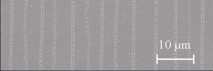
6 in 48% hydrofluoric acid (HF) and inspected with optical and scanning electron microscopy (SEM). Results and discussion Initial experiments were conducted to establish the single pulse ablation threshold for the +z face of lithium niobate samples at both laser wavelengths. It is important to note at this point that AOP occurs near the ablation threshold. The single pulse ablation thresholds for 266 nm and 298 nm light were established experimentally to be between mj/cm 2. However, these figures are subject to some degree of uncertainty due to the intrinsic spatial non-uniformity and temporal (pulse to pulse) fluctuation of the dye laser. As with typical material ablation studies, these thresholds were observed to decrease for multi-pulse exposures. Areas irradiated through the phase-mask at fluences significantly below the ablation threshold showed no evidence of domain formation. There exists, however, a narrow range of fluences (~ mj/cm 2 ) between which domain formation parallel to the phase-mask lines is possible with some degree of ablation damage. Considerably above the ablation threshold for a single pulse, weak domain formation was also observed, but it was accompanied by a pronounced ablation grating. Nevertheless, it is rather easy to distinguish between the laser damage pattern as subsequently revealed by the chemical etching and the ferroelectric pattern because etched ferroelectric domains are deeper and sharper than the ablated trenches. The effect of UV illumination without the use of phase mask is shown in figure 1a. Here an SEM scan of the irradiated surface after HF acid etching is presented showing 6
7 the random nucleation and propagation of photo-induced domains along the three equivalent symmetry directions of the crystal. This effect has been extensively discussed before in reference [15]. Figure 1b shows an SEM image of the crystal surface that has been irradiated using a phase mask. The difference between these two images is readily apparent. Figure 1b shows that the majority of the photo-induced domains are aligned along a specific y-axis (vertical in the figure), dictated by the orientation of the phase mask which coincides with one of the crystal symmetry axes as shown in the inset direction indicator (top right). This was expected as the AOP domains nucleate only in the presence of near damage threshold optical intensity and propagate along the symmetry directions. In this experiment there is light only along a specific symmetry direction where the AOP domains are encouraged to nucleate and propagate resulting in the direction preference observed. However, careful investigation of this domain formation details shows that the effect is more complex than initially expected. The SEM image presented in Figure 2 shows a magnified section of figure 1b. Although the domain lines formed are parallel to the phase mask lines, it is clear that the periodicity imposed by the phase mask (Λ = µm) has not been faithfully reproduced in the resultant domain spacing. While measured domain widths are again in the range from nm, the distance between them varies between ~2 µm and ~9.4 µm. This behaviour appears to underlie all such AOP experiments performed to date. Imposition of a spatially extended light pattern with sub-micron periodicity, such as from the phase mask, appears to be opposed by the physical mechanism responsible for AOP. This is suggestive of an electrostatic mechanism, as the photo-generated 7
8 surface charge, likely to occur at the highly UV-absorbing surface, will result in electrostatic repulsion and re-organisation (e.g. clustering around surface defects). This imposes a characteristic electrostatic interaction length that overrides the imposed periodicity of the intensity pattern as the material is unable to both nucleate and sustain such closely packed domains via a strictly AOP process only. Another interesting observation can be made in figure 2 which also suggests electrostatic interaction between individual domains, namely that the domain lines produced are not continuous, but consist of irregular sections along the y-axis direction which is suggestive of correlated nucleation in highly non-equilibrium domain inversion reported in [16]. Of interest is the difference between apparently straight domain patterning at approximate values of 10Λ, and irregular domain lines that develop between them, as can also be seen in figure 2. This observation indicates that the initial conditions such as the sequence of nucleation and propagation of the domains are important. One possible explanation for the formation of the irregular domain lines between the straight lines could be that they were developed under the electrostatic influence of the previously formed straight lines. Further investigation of the surface topography suggests that local intensity level variations significantly affect the AOP domain formation. Since there are variations of the local intensity across the laser spot (e.g. from the centre to the edge), different parts of the illuminated surface correspond to different conditions for nucleation and propagation of the photo-induced domains. In the case of Figure 2, AOP domains are 8
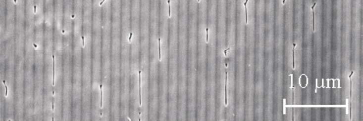
9 observed without the presence of ablation, hence indicating that ablation is not a necessary requirement for AOP. The varying intensity profile across the laser beam allows investigation of the effect of local intensity variation on the AOP domain development. Figure 3 shows a part of the etched surface corresponding to the edge of an irradiated area exposed through a phase mask, and therefore experienced a slightly lower fluence. The area was illuminated with two pulses at λ = 298 nm at a fluence of ~160 mj/cm 2. It becomes immediately clear after observing the SEM image (figure 3) that nucleation, and occasional limited subsequent propagation of domains, occurs only at positions of maximum light intensity. For this specific local exposure condition, simultaneous nucleation of sub-micron domains (top left) was obtained which are located in close proximity, even on adjacent phase mask intensity maxima. An area where both nucleation and growth (propagation) occur can also be observed in the same figure (bottom right), however these expanded domains are spaced further apart, resembling the situation shown in figure 2 where the domain lines maintain a distance of µm. In a subsequent experiment the phase-mask was rotated so that the grating lines were at an angle of approximately 38 with respect to the crystallographic y-axis of the exposed sample. The purpose of this experiment was to conclude whether the crystal symmetry prevails over the spatial modulation of the optical intensity pattern, in other words to show whether arbitrarily-aligned domain patterns can be produced. In this experiment a single 266 nm pulse of fluence ~150 mj/cm 2 was applied to generate a clearly visible ablation grating which was used to identify the rotation angle. 9
10 Investigation of the surface topography after etching showed that it is not possible to override the symmetry directions of the crystal. As in all previous cases the AOP domains nucleate on the maxima of the optical intensity but they cannot be encouraged to propagate along the direction imposed by the optical intensity distribution unless this direction coincides with one of the y-axes of symmetry. Figure 4 shows a detailed SEM scan of the HF-etched surface where the ablation grating is clearly visible and the y-axis directions are indicated in the inset diagram (top left). Investigation of figure 4 confirms the earlier statement that sub-micron (~300 nm) AOP domains are located on the maxima of the optical intensity pattern but they can only propagate along the y-directions which in this case is not possible due to the absence of light in the dark fringes of the illuminating optical intensity pattern produced by the phase mask. However, it is interesting to note that individual adjacent domains are aligned along these three y-directions of the crystal at a fixed period imposed by the intensity pattern. Hence it may be possible to have dense packing of periodic domains along the y symmetry directions, for example, by 2D periodic illumination. As noted previously, all optical ferroelectric domain reversal occurs only at the maxima of the laser intensity distribution as produced by the phase-mask. However, the separation between adjacent domains, although always a multiple of the phase mask period, is variable. A systematic study of the domain separation along the x-axis was performed on samples fabricated using a range of laser fluences (~100 ~150 mj/cm 2 ). This study revealed that the distribution of domain separation does not 10
11 depend on the laser energy fluence. The observed separation distributions have shown a maximum of 10% deviation from the average domain separation across this range of fluences, with no difference between single or double-pulse exposures. The average of domain separation distribution over different samples is shown in the histogram of figure 5. This histogram indicates that 88% of the measured domain separation widths lie between 4Λ - 8Λ (2.9 µm- 5.8 µm). Significantly, as shown in the histogram there are no separations between domain lines under 3Λ (2.18 µm), underlining the hypothesis of a minimum domain formation distance. The effect of temperature on the formation of AOP domains was also investigated by a simple experiment. The crystal/phase mask assembly was placed on a hot plate, and exposures were performed at different equilibrium temperatures ranging from room temperature to 200 C. No qualitative difference was observed at temperatures below 100 C. However as the temperature increased, it was observed that the domain density is significantly reduced and domain lines tend to develop even further apart than in the room temperature case. The major difference is that the domain lines do not consist of individual sections but form continuous lines. Figure 6 shows an SEM micrograph of continuous domain lines as a result of irradiation at a temperature of 190 C. All the experimental results so far have not been able to provide a conclusive physical interpretation of the effect. Nevertheless there are numerous indications suggesting that the AOP process originates from charge imbalance which is the result of the removal of surface charge compensating crystal layers via ablation. Other effects such 11
12 as Li 2 O out-diffusion or side diffusion, the pyroelectric and piezoelectric effect which occur upon absorption of an intense UV pulse and subsequent rapid temperature rise may also contribute to the formation of AOP domains [17]. Conclusions Ordered alignment of AOP domains has been achieved by spatially modulated UV laser radiation using a phase mask. The pulsed UV laser-induced domains nucleate on optical intensity maxima and are encouraged to grow along a specific y direction of the crystal specified by the aligned orientation of a periodic optical intensity pattern. However, full replication of the optical periodic pattern was not achieved due to possible electrostatic repulsion between adjacent domains which limits the minimum distance between them to ~2 µm for the range of illumination conditions used in our experiments. Furthermore, for experiments performed at room temperature the ordered domain lines consist of discrete smaller domains, while at higher temperatures domain lines are continuous but tend to grow even further apart from each other. Experimental results suggest that although long domain lines cannot grow in close proximity due to electrostatic limitations, it may be possible to achieve denser packing of individual domains (domains which have just nucleated but not expanded) by illuminating with a 2D periodic intensity pattern. Further work is required for the complete understanding of the physical mechanism behind this very interesting effect. The investigation which is presented here is an 12
13 important first step towards successful manipulation and control of AOP ferroelectric domains in congruent lithium niobate. Acknowledgements The authors are grateful to the Engineering and Physical Sciences Research Council (EPSRC) for research funding via grant EP/C515668/1 and to Dr Ian Clark and the Rutherford Appleton Central Laser Facility for the Continuum Powerlite 8000 dye laser loan. 13
14 References 1. K. Yamamoto, K. Mizuuchi, K. Takeshige, Y. Sasi, and T. Taniuchi, J. Appl. Phys. 70(4), 1947, (1991) 2. K. Nakamura, and H. Shimizu, Appl. Phys. Lett. 56(16), 1535, (1990) 3. S. Miyazawa, J. Appl. Phys. 50(7). 4599, (1979) 4. K. Terabe, M. Nakamura, S. Takekawa, K. Kitamura, S. Higuchi, Y. Gotoh, and Y. Cho, Appl. Phys. Lett. 82 (3), 433, (2003) 5. M. Yamada, and K. Kishima, Electron. Lett. 27(10), 828, (1991) 6. H. Ito, C. Takyu, and H. Inaba, Electron. Lett. 27(14), 1221, (1991) 7. M. Yamada, N. Nada, M. Saitoh, and K. Watanabe, Appl. Phys. Lett. 62(5), 435, (1993) 8. S. Chao, W. Davis, D. D Tuschel, R. Nichols, M. Gupta, and H. C Cheng, Appl. Phys. Lett. 67, 1066, (1995) 9. P. T Brown, G. W Ross, R. W Eason, and A. R Pogosyan, Opt. Commun. 163(4-6), 310, (1999) 10. M. Müller, E. Soergel, and K. Buse, Appl. Phys. Lett. 83(9), 1824, (2003) 11. A. Fujimura, T. Sohmura, and T. Suhara, Electron. Lett, 39 (9). 719, (2003) 12. M. C. Wengler, B. Fassbender, E. Soergel, and K. Buse, J. Appl. Phys. 96, 2816, (2004) 13. V. Dierolf, and C. Sandmann, Appl. Phys. Lett. 84(20), 3987, (2004) 14. C. L. Sones, M. C. Wengler, C. E. Valdivia, S. Mailis, R. W. Eason, and K. Buse, Appl. Phys. Lett. 86(21), (2005) 15. C. E. Valdivia, C. L. Sones, J. G. Scott, S. Mailis, R. W. Eason, D. A. Scrymgeour, V. Gopalan, T. Jungk, E. Soergel, and I. Clark, Appl. Phys. Lett. 86(2), , (2005) 14
15 16. V. Ya. Shur, Correlated nucleation and self-organized kinetics of ferroelectric domains in Nucleation Theory and Applications, J. W. P. Schmelzer, Wiley, , (2005) 17. K. Nakamura, H. Ando, H. Shimizu, Appl. Phys. Lett. 50(20), 1413, (1987) 15
16 List of figures Figure 1: SEM micrographs of the etched +z face following a) illumination with a non-spatially-modulated beam, and b) illumination via a phase mask. The three symmetrical y-axes are indicated on the top right of the figure. Both exposures were performed with the frequency-quadrupled Nd:YVO 4 laser at λ = 266 nm, with energy fluence values above the threshold for ablation. Figure 2: High magnification SEM micrograph of aligned discrete domain patterned region within the central area of a sample exposed via a phase mask at a laser fluence of ~100 mj/cm 2 without observable surface damage. The directions of the y axes are indicated on the top right. Figure 3: SEM micrograph taken at the edge of the phase mask irradiated area using λ=298 nm. The directions of the y axes are indicated on the top right. Figure 4: SEM micrograph of the +z face illuminated through a phase mask which has been misaligned with respect to a y-axis by ~38. The three y directions are indicated on the top left of the figure. Figure 5: Histogram showing the occurrence probability of different domain separation widths, normalized to the period of the phase mask (PM). The data shown here are the average of measurements performed on samples produced with a range of laser fluences (~100 mj/cm 2 - ~150 mj/cm 2 ). 16
17 Figure 6: SEM micrograph of +z face illuminated through a phase mask with single 266 nm pulse (~110 mj/cm 2 ) at a sample temperature of 190 C. The directions of the y axes are indicated on the top left. 17

18 Fig 1a. 18

19 Fig 1b. 19

20 Fig 2. 20

21 Fig 3. 21

22 Fig 4. 22
23 Fig 5. 23
24 Fig 6. 24
Ferroelectric domain and surface nano-engineering of a near-stoichiometric LiNbO 3 single crystal
 Ferroelectric domain and surface nano-engineering of a near-stoichiometric LiNbO 3 single crystal K. Terabe*, M. Nakamura, S. Takekawa, and K. Kitamura, National Institute for Materials Science, Japan;
Channel Optical Waveguides with Spatial Longitudinal Modulation of Their Parameters Induced in Photorefractive Lithium Niobate Samples
 Russian Forum of Young Scientists Volume 2018 Conference Paper Channel Optical Waveguides with Spatial Longitudinal Modulation of Their Parameters Induced in Photorefractive Lithium Niobate Samples A D
Periodic Poling of Stoichiometric Lithium Tantalate for High-Average Power Frequency Conversion
 VG04-123 Periodic Poling of Stoichiometric Lithium Tantalate for High-Average Power Frequency Conversion Douglas J. Bamford, David J. Cook, and Scott J. Sharpe Physical Sciences Inc. Jeffrey Korn and Peter
Contrast Mechanism for Visualization of Ferroelectric Domains with Scanning Force Microscopy
 Ferroelectrics, 334:29 34, 2006 Copyright Taylor & Francis Group, LLC ISSN: 0015-0193 print / 1563-5112 online DOI: 10.1080/00150190600689654 Contrast Mechanism for Visualization of Ferroelectric Domains
Quasi-phase matching via femtosecond laser induced domain inversion in lithium niobate waveguides
 Letter Optics Letters 1 Quasi-phase matching via femtosecond laser induced domain inversion in lithium niobate waveguides XIN CHEN 1,PAWEL KARPINSKI 1,2,VLADLEN SHVEDOV 1,ANDREAS BOES 3,ARNAN MITCHELL
Multi-cycle THz pulse generation in poled lithium niobate crystals
 Laser Focus World April 2005 issue (pp. 67-72). Multi-cycle THz pulse generation in poled lithium niobate crystals Yun-Shik Lee and Theodore B. Norris Yun-Shik Lee is an assistant professor of physics
Electrically induced and tunable photonic band gap in submicron periodically poled lithium niobate
 Appl Phys B (2009) 96: 787 791 DOI 10.1007/s00340-009-3622-9 Electrically induced and tunable photonic band gap in submicron periodically poled lithium niobate Z. Zhou J. Shi X. Chen Received: 11 July
X-Rays From Laser Plasmas
 X-Rays From Laser Plasmas Generation and Applications I. C. E. TURCU CLRC Rutherford Appleton Laboratory, UK and J. B. DANCE JOHN WILEY & SONS Chichester New York Weinheim Brisbane Singapore Toronto Contents
PHYSICAL BASIS OF THE DOMAIN ENGINEERING IN THE BULK FERROELECTRICS
 Ferroelectrics, V. 221, pp. 157-167 (1999) PHYSICAL BASIS OF THE DOMAIN ENGINEERING IN THE BULK FERROELECTRICS VLADIMIR SHUR, a EVGENII RUMYANTSEV, a ROBERT BATCHKO, b GREGORY MILLER, b MARTIN FEJER b
Reflection second harmonic generation on a z-cut congruent lithium niobate crystal
 Reflection second harmonic generation on a z-cut congruent lithium niobate crystal T. J. Sono*, J. G. Scott, C. L. Sones, C. E. Valdivia, S. Mailis and R. W. Eason Optoelectronics Research Centre, University
Generation of visible and mid-infrared radiation in periodically poled stoichiometric lithium tantalate
 PSI-SR-109 Generation of visible and mid-infrared radiation in periodically poled stoichiometric lithium tantalate Douglas J. Bamford David J. Cook Scott J. Sharpe Aaron Van Pelt Douglas J. Bamford, David
Morphology-dependent resonance induced by two-photon excitation in a micro-sphere trapped by a femtosecond pulsed laser
 Morphology-dependent resonance induced by two-photon excitation in a micro-sphere trapped by a femtosecond pulsed laser Dru Morrish, Xiaosong Gan and Min Gu Centre for Micro-Photonics, School of Biophysical
Periodic poling of magnesium-oxide-doped lithium niobate
 JOURNAL OF APPLIED PHYSICS VOLUME 91, NUMBER 7 1 APRIL 2002 Periodic poling of magnesium-oxide-doped lithium niobate Koichiro Nakamura, a) Jonathan Kurz, Krishnan Parameswaran, and M. M. Fejer Edward L.
Optical sensor based on hybrid LPG/FBG in D-fiber for simultaneous refractive index and temperature measurement
 Optical sensor based on hybrid G/FBG in D-fiber for simultaneous refractive index and temperature measurement Xianfeng Chen*, Kaiming Zhou, Lin Zhang, Ian Bennion Photonics Research Group, Aston University,
Recent Achievements in Domain Engineering in Lithium Niobate and Lithium Tantalate
 Ferroelectrics, 2001, Vol. 257, pp. 191-202 Reprints available directly from the publisher Photocopying permitted by license only 2001 Taylor & Francis Recent Achievements in Domain Engineering in Lithium
Online publication date: 23 June 2010 PLEASE SCROLL DOWN FOR ARTICLE
 This article was downloaded by: [Shur, Vladimir][NEICON Consortium] On: 24 June 2010 Access details: Access Details: [subscription number 781557264] Publisher Taylor & Francis Informa Ltd Registered in
2008,, Jan 7 All-Paid US-Japan Winter School on New Functionalities in Glass. Controlling Light with Nonlinear Optical Glasses and Plasmonic Glasses
 2008,, Jan 7 All-Paid US-Japan Winter School on New Functionalities in Glass Photonic Glass Controlling Light with Nonlinear Optical Glasses and Plasmonic Glasses Takumi FUJIWARA Tohoku University Department
Chapter 1 Micro-Structuring and Ferroelectric Domain Engineering of Single Crystal Lithium Niobate
 Chapter 1 Micro-Structuring and Ferroelectric Domain Engineering of Single Crystal Lithium Niobate S. Mailis, C.L. Sones, and R.W. Eason 1.1 Introduction The ability to microstructure specific materials
Thermodynamics Study on the Decay Properties of Reversed Domains in LiNbO 3. Single Crystals
 DOI: 1.4172/221-6212.1178 Thermodynamics Study on the Decay Properties of Reversed Domains in LiNbO Single rystals Li LB 1,2*, Li GL 1, Kan Y 2, Lu XM 2 and Zhu JS 2 1 School of Physics and Engineering,
Domain patterning in lithium niobate using spontaneous backswitching
 Domain patterning in lithium niobate using spontaneous backswitching R.G. Batchko*, G.D. Millerb, V. Ya. Shur', E. L. Rumyantsevc M.M. Fejer', and R.L. Byera ael Ginzton Laboratory, Stanford University,
Title of file for HTML: Supplementary Information Description: Supplementary Figures and Supplementary References
 Title of file for HTML: Supplementary Information Description: Supplementary Figures and Supplementary References Supplementary Figure 1. SEM images of perovskite single-crystal patterned thin film with
Laboratory 3: Confocal Microscopy Imaging of Single Emitter Fluorescence and Hanbury Brown, and Twiss Setup for Photon Antibunching
 Laboratory 3: Confocal Microscopy Imaging of Single Emitter Fluorescence and Hanbury Brown, and Twiss Setup for Photon Antibunching Jonathan Papa 1, * 1 Institute of Optics University of Rochester, Rochester,
Structural dynamics of PZT thin films at the nanoscale
 Mater. Res. Soc. Symp. Proc. Vol. 902E 2006 Materials Research Society 0902-T06-09.1 Structural dynamics of PZT thin films at the nanoscale Alexei Grigoriev 1, Dal-Hyun Do 1, Dong Min Kim 1, Chang-Beom
Diffractive self-imaging based on selective etching of a ferroelectric domain inversion grating
 COL 13(2), 02002(201) CHINESE OPTICS LETTERS February 10, 201 Diffractive self-imaging based on selective etching of a ferroelectric domain inversion grating Yunlin Chen ( 陈云琳 )*, Tianwei Fan ( 范天伟 ),
Design of Uniform Fiber Bragg grating using Transfer matrix method
 International Journal of Computational Engineering Research Vol, 3 Issue, 5 Design of Uniform Fiber Bragg grating using Transfer matrix method Deba Kumar Mahanta Department of Electrical Engineering, Assam
Nonlinear Physical Optics With Transversely Patterned Quasi-Phase-Matching Gratings
 660 IEEE JOURNAL OF SELECTED TOPICS IN QUANTUM ELECTRONICS, VOL. 8, NO. 3, MAY/JUNE 2002 Nonlinear Physical Optics With Transversely Patterned Quasi-Phase-Matching Gratings Jonathan R. Kurz, Andrew M.
Nanocomposite photonic crystal devices
 Nanocomposite photonic crystal devices Xiaoyong Hu, Cuicui Lu, Yulan Fu, Yu Zhu, Yingbo Zhang, Hong Yang, Qihuang Gong Department of Physics, Peking University, Beijing, P. R. China Contents Motivation
Bannerman High School Physics Department. Making Accurate Statements. Higher Physics. Quanta and Waves
 Bannerman High School Physics Department Making Accurate Statements Higher Physics Quanta and Waves Mandatory Key Area: Particle Physics 1. Use your knowledge of physics to estimate the ratio of the smallest
Study of lithium niobate crystals
 Study of lithium niobate crystals Ekaterina Kochetkova Lomonosov Moscow State University, Russia DESY, Hamburg, Germany September 5, 2017 Abstract This report describes the study of the optical properties
Simultaneous Temperature and Strain Sensing for Cryogenic Applications Using Dual-Wavelength Fiber Bragg Gratings
 Simultaneous Temperature and Strain Sensing for Cryogenic Applications Using Dual-Wavelength Fiber Bragg Gratings Meng-Chou Wu *, William H. Prosser NASA, Langley Research Center, MS 231, Hampton, VA,
Transformation dependence of lead zirconate titanate (PZT) as shown by PiezoAFM surface mapping of Sol-gel produced PZT on various substrates.
 as shown by PiezoAFM surface mapping of Sol-gel produced PZT on various substrates.") Transformation dependence of lead zirconate titanate (PZT) as shown by PiezoAFM surface mapping of Sol-gel produced PZT on various substrates. Abstract S. Dunn and R. W. Whatmore Building 70, Nanotechnology,
Transformation dependence of lead zirconate titanate (PZT) as shown by PiezoAFM surface mapping of Sol-gel produced PZT on various substrates. Abstract S. Dunn and R. W. Whatmore Building 70, Nanotechnology,
A Novel Self-aligned and Maskless Process for Formation of Highly Uniform Arrays of Nanoholes and Nanopillars
 Nanoscale Res Lett (2008) 3: 127 DOI 10.1007/s11671-008-9124-6 NANO EXPRESS A Novel Self-aligned and Maskless Process for Formation of Highly Uniform Arrays of Nanoholes and Nanopillars Wei Wu Æ Dibyendu
Tailoring of optical properties of LiNbO 3 by ion implantation
 SMR/1758-14 "Workshop on Ion Beam Studies of Nanomaterials: Synthesis, Modification and Characterization" 26 June - 1 July 2006 Tailoring of Optical Properties of LiNbO3 by ion implantation Cinzia SADA
Important processes in modeling and optimization of EUV lithography sources
 Important processes in modeling and optimization of UV lithography sources T. Sizyuk and A. Hassanein Center for Materials under xtreme nvironment, School of Nuclear ngineering Purdue University, West
Micro-patterned porous silicon using proton beam writing
 Micro-patterned porous silicon using proton beam writing M. B. H. Breese, D. Mangaiyarkarasi, E. J. Teo*, A. A. Bettiol and D. Blackwood* Centre for Ion Beam Applications, Department of Physics, National
Femtosecond laser microfabrication in. Prof. Dr. Cleber R. Mendonca
 Femtosecond laser microfabrication in polymers Prof. Dr. Cleber R. Mendonca laser microfabrication focus laser beam on material s surface laser microfabrication laser microfabrication laser microfabrication
Chapter 2 Process Variability. Overview. 2.1 Sources and Types of Variations
 Chapter 2 Process Variability Overview Parameter variability has always been an issue in integrated circuits. However, comparing with the size of devices, it is relatively increasing with technology evolution,
On Domain Wall Broadening in Ferroelectric Lithium Niobate and Tantalate
 Page 277, AIP Conference Proceedings, Fundamental Physics of Ferroelectrics 2002. On Domain Wall Broadening in Ferroelectric Lithium Niobate and Tantalate Sungwon Kim*, B. Steiner, A. Gruverman, V. Gopalan*
Microfabricação em materiais poliméricos usando laser de femtossegundos
 Microfabricação em materiais poliméricos usando laser de femtossegundos Prof. Cleber R. Mendonça http://www.fotonica.ifsc.usp.br University of Sao Paulo - Brazil students 77.000 52.000 undergrad. 25.000
Domain switching and electromechanical properties of pulse poled Pb Zn 1Õ3 Nb 2Õ3 O 3 PbTiO 3 crystals
 JOURNAL OF APPLIED PHYSICS VOLUME 89, NUMBER 1 1 JANUARY 2001 Domain switching and electromechanical properties of pulse poled Pb Zn 1Õ3 Nb 2Õ3 O 3 PbTiO 3 crystals Hanxing Yu, Venkat Gopalan, Jürgen Sindel,
Simultaneous optical parametric oscillation and intracavity second-harmonic generation based on a hexagonally poled lithium tantalate
 Simultaneous optical parametric oscillation and intracavity second-harmonic generation based on a hexagonally poled lithium tantalate P. Xu *, J. F. Wang, C. Li, Z. D. Xie, X. J. Lv, H. Y. Leng, J. S.
CHAPTER 7 SUMMARY OF THE PRESENT WORK AND SUGGESTIONS FOR FUTURE WORK
 161 CHAPTER 7 SUMMARY OF THE PRESENT WORK AND SUGGESTIONS FOR FUTURE WORK 7.1 SUMMARY OF THE PRESENT WORK Nonlinear optical materials are required in a wide range of important applications, such as optical
Semiconductor Disk Laser on Microchannel Cooler
 Semiconductor Disk Laser on Microchannel Cooler Eckart Gerster An optically pumped semiconductor disk laser with a double-band Bragg reflector mirror is presented. This mirror not only reflects the laser
Theoretical Analysis of the TE Mode Cerenkov Type Second Harmonic Generation in Ion-Implanted X-Cut Lithium Niobate Planar Waveguides
 Vol. 115 (2009) ACTA PHYSICA POLONICA A No. 3 Theoretical Analysis of the TE Mode Cerenkov Type Second Harmonic Generation in Ion-Implanted X-Cut Lithium Niobate Planar Waveguides G. Du, G. Li, S. Zhao,
Research Article Domain-Reversed Lithium Niobate Single-Crystal Fibers are Potentially for Efficient Terahertz Wave Generation
 Advances in OptoElectronics Volume 008, Article ID 08458, 5 pages doi:10.1155/008/08458 Research Article Domain-Reversed Lithium Niobate Single-Crystal Fibers are Potentially for Efficient Terahertz Wave
SUPPLEMENTAL MATERIAL I: SEM IMAGE OF PHOTONIC CRYSTAL RESONATOR
 1 SUPPLEMENTAL MATERIAL I: SEM IMAGE OF PHOTONIC CRYSTAL RESONATOR Figure S1 below is a scanning electronic microscopy image of a typical evanescently coupled photonic crystal resonator used in these experiments.
Focusing of Light by a Nano-Hole Array
 Focusing of Light by a Nano-Hole Array Fu Min Huang 1, Yifang Chen 2, F. Javier Garcia de Abajo 3 and Nikolay Zheludev 1 1 EPSRC Nanophotonics Portfolio Centre, School of Physics and Astronomy, University
Measurement of the 2 tensors of KTiOPO 4, KTiOAsO 4, RbTiOPO 4, and RbTiOAsO 4 crystals
 Measurement of the 2 tensors of KTiOPO 4, KTiOAsO 4, RbTiOPO 4, and RbTiOAsO 4 crystals Michael V. Pack, Darrell J. Armstrong, and Arlee V. Smith We use the separated-beams method to measure the second-order
Multi-Purpose Nonlinear Optical Microscope. Principle and its Applications to Polar Thin Film Observation
 Multi-Purpose Nonlinear Optical Microscope. Principle and its Applications to Polar Thin Film Observation Y. Uesu, N. Kato Department of Physics, Waseda University 3 4 1 Okubo, Shinjuku-ku, Tokyo 169-8555,
Free Electron Laser. Project report: Synchrotron radiation. Sadaf Jamil Rana
 Free Electron Laser Project report: Synchrotron radiation By Sadaf Jamil Rana History of Free-Electron Laser (FEL) The FEL is the result of many years of theoretical and experimental work on the generation
Confocal Microscopy Imaging of Single Emitter Fluorescence and Hanbury Brown and Twiss Photon Antibunching Setup
 1 Confocal Microscopy Imaging of Single Emitter Fluorescence and Hanbury Brown and Twiss Photon Antibunching Setup Abstract Jacob Begis The purpose of this lab was to prove that a source of light can be
High-Speed Quadratic Electrooptic Nonlinearity in dc-biased InP
 Vol. 107 (2005) ACTA PHYSICA POLONICA A No. 2 Proceedings of the 12th International Symposium UFPS, Vilnius, Lithuania 2004 High-Speed Quadratic Electrooptic Nonlinearity in dc-biased InP L. Subačius a,,
Dept. of Physics, MIT Manipal 1
 Chapter 1: Optics 1. In the phenomenon of interference, there is A Annihilation of light energy B Addition of energy C Redistribution energy D Creation of energy 2. Interference fringes are obtained using
Tuning of 2-D Silicon Photonic Crystals
 Mat. Res. Soc. Symp. Proc. Vol. 722 2002 Materials Research Society Tuning of 2-D Silicon Photonic Crystals H. M. van Driel, S.W. Leonard, J. Schilling 1 and R.B. Wehrspohn 1 Department of Physics, University
SUPPLEMENTARY INFORMATION
 doi:10.1038/nature12036 We provide in the following additional experimental data and details on our demonstration of an electrically pumped exciton-polariton laser by supplementing optical and electrical
Chapter 3 Chapter 4 Chapter 5
 Preamble In recent years bismuth-based, layer-structured perovskites such as SrBi 2 Nb 2 O 9 (SBN) and SrBi 2 Ta 2 O 9 (SBT) have been investigated extensively, because of their potential use in ferroelectric
Laser-induced Ferroelectric and Photonic Structures in Lithium Niobate Crystals
 UNIVERSITY OF SOUTHAMPTON FACULTY OF PHYSICAL SCIENCES AND ENGINEERING Optoelectronics Research Centre Laser-induced Ferroelectric and Photonic Structures in Lithium Niobate Crystals by Zisis Grigorios
Domain wall characterization in ferroelectrics by using localized nonlinearities
 Domain wall characterization in ferroelectrics by using localized nonlinearities Xuewei Deng and Xianfeng Chen* Department of Physics, the State Key Laboratory on Fiber Optic Local Area Communication Networks
Photonic Crystals. Introduction
 Photonic Crystals Introduction Definition Photonic crystals are new, artificialy created materials, in which refractive index is periodically modulated in a scale compared to the wavelength of operation.
Neodymium Laser Q-Switched with a Cr 4+ : YAG Crystal: Control over Polarization State by Exterior Weak Resonant Radiation
 Laser Physics, Vol., No.,, pp. 46 466. Original Text Copyright by Astro, Ltd. Copyright by MAIK Nauka /Interperiodica (Russia). SOLID STATE LASERS AND NONLINEAR OPTICS Neodymium Laser Q-Switched with a
Towards the Lasing Spaser: Controlling. Metamaterial Optical Response with Semiconductor. Quantum Dots
 Towards the Lasing Spaser: Controlling Metamaterial Optical Response with Semiconductor Quantum Dots E. Plum, V. A. Fedotov, P. Kuo, D. P. Tsai, and N. I. Zheludev,, Optoelectronics Research Centre, University
EXTREME ULTRAVIOLET AND SOFT X-RAY LASERS
 Chapter 7 EXTREME ULTRAVIOLET AND SOFT X-RAY LASERS Hot dense plasma lasing medium d θ λ λ Visible laser pump Ch07_00VG.ai The Processes of Absorption, Spontaneous Emission, and Stimulated Emission Absorption
Section 2 ADVANCED TECHNOLOGY DEVELOPMENTS
 Section 2 ADVANCED TECHNOLOGY DEVELOPMENTS 2.A Application of KTP Crystal as an Electro-Optic Amplitude Modulator Potassium titanyl phosphate (KTiOP04 or KTP) has become a widely used nonlinear optical
Ion exchange model for phase proton exchange waveguide in LiNbO3.
 Downloaded from orbit.dtu.dk on: Jul 10, 2018 Ion exchange model for phase proton exchange waveguide in LiNbO3. Veng, Torben Erik; Skettrup, Torben Published in: Journal of Lightwave Technology Link to
Visualization of Xe and Sn Atoms Generated from Laser-Produced Plasma for EUV Light Source
 3rd International EUVL Symposium NOVEMBER 1-4, 2004 Miyazaki, Japan Visualization of Xe and Sn Atoms Generated from Laser-Produced Plasma for EUV Light Source H. Tanaka, A. Matsumoto, K. Akinaga, A. Takahashi
Quantitative Measurement of the Surface Charge Density. Abstract
 APS/123-QED Quantitative Measurement of the Surface Charge Density Florian Johann and Elisabeth Soergel Institute of Physics, University of Bonn, Wegelerstraße 8, 53115 Bonn, Germany arxiv:1009.1902v1
A microring multimode laser using hollow polymer optical fibre
 PRAMANA c Indian Academy of Sciences Vol. 75, No. 5 journal of November 2010 physics pp. 923 927 A microring multimode laser using hollow polymer optical fibre M KAILASNATH, V P N NAMPOORI and P RADHAKRISHNAN
Laser matter interaction
 Laser matter interaction PH413 Lasers & Photonics Lecture 26 Why study laser matter interaction? Fundamental physics Chemical analysis Material processing Biomedical applications Deposition of novel structures
Initial Results on the Feasibility of Hybrid X-Ray Microscopy
 CHINESE JOURNAL OF PHYSICS VOL. 43, NO. 5 OCTOBER 2005 Initial Results on the Feasibility of Hybrid X-Ray Microscopy P. K. Tseng, 1 W. F. Pong, 1 C. L. Chang, 1 C. P. Hsu, 1 F. Y. Lin, 2 C. S. Hwang, 2
Quantum Optics and Quantum Information Laboratory
 Quantum Optics and Quantum Information Laboratory OPT 253, Fall 2011 Institute of Optics University of Rochester Instructor: Dr. Lukishova Jonathan Papa Contents Lab 1: Entanglement and Bell s Inequalities
Dielectric Accelerators at CLARA. G. Burt, Lancaster University On behalf of ASTeC, Lancaster U., Liverpool U., U. Manchester, and Oxford U.
 Dielectric Accelerators at CLARA G. Burt, Lancaster University On behalf of ASTeC, Lancaster U., Liverpool U., U. Manchester, and Oxford U. Dielectric Accelerators Types Photonic structures Dielectric
Photonic Crystal Nanocavities for Efficient Light Confinement and Emission
 Journal of the Korean Physical Society, Vol. 42, No., February 2003, pp. 768 773 Photonic Crystal Nanocavities for Efficient Light Confinement and Emission Axel Scherer, T. Yoshie, M. Lončar, J. Vučković
A Photonic Crystal Laser from Solution Based. Organo-Lead Iodide Perovskite Thin Films
 SUPPORTING INFORMATION A Photonic Crystal Laser from Solution Based Organo-Lead Iodide Perovskite Thin Films Songtao Chen 1, Kwangdong Roh 2, Joonhee Lee 1, Wee Kiang Chong 3,4, Yao Lu 5, Nripan Mathews
Polarization control and sensing with two-dimensional coupled photonic crystal microcavity arrays. Hatice Altug * and Jelena Vučković
 Polarization control and sensing with two-dimensional coupled photonic crystal microcavity arrays Hatice Altug * and Jelena Vučković Edward L. Ginzton Laboratory, Stanford University, Stanford, CA 94305-4088
Investigation of Optical Nonlinearities and Carrier Dynamics in In-Rich InGaN Alloys
 Vol. 113 (2008) ACTA PHYSICA POLONICA A No. 3 Proceedings of the 13th International Symposium UFPS, Vilnius, Lithuania 2007 Investigation of Optical Nonlinearities and Carrier Dynamics in In-Rich InGaN
A FEM STUDY ON THE INFLUENCE OF THE GEOMETRIC CHARACTERISTICS OF METALLIC FILMS IRRADIATED BY NANOSECOND LASER PULSES
 8 th GRACM International Congress on Computational Mechanics Volos, 12 July 15 July 2015 A FEM STUDY ON THE INFLUENCE OF THE GEOMETRIC CHARACTERISTICS OF METALLIC FILMS IRRADIATED BY NANOSECOND LASER PULSES
OPTI510R: Photonics. Khanh Kieu College of Optical Sciences, University of Arizona Meinel building R.626
 OPTI510R: Photonics Khanh Kieu College of Optical Sciences, University of Arizona kkieu@optics.arizona.edu Meinel building R.626 Announcements HW#3 is assigned due Feb. 20 st Mid-term exam Feb 27, 2PM
SUPPLEMENTARY INFORMATION
 doi:10.1038/nature11231 Materials and Methods: Sample fabrication: Highly oriented VO 2 thin films on Al 2 O 3 (0001) substrates were deposited by reactive sputtering from a vanadium target through reactive
Ho:YLF pumped HBr laser
 Ho:YLF pumped HBr laser L R Botha, 1,2,* C Bollig, 1 M J D Esser, 1 R N Campbell 4, C Jacobs 1,3 and D R Preussler 1 1 National Laser Centre, CSIR, Pretoria, South Africa 2 Laser Research Institute, Department
Supporting information
 Supporting information Vacuum ultraviolet laser desorption/ionization mass spectrometry imaging of single cells with submicron craters Jia Wang, 1, + Zhaoying Wang, 2, + Feng Liu, 1 Lesi Cai, 2 Jian-bin
Supplementary Figure 1. A photographic image of directionally grown perovskite films on a glass substrate (size: cm).
.") Supplementary Figure 1. A photographic image of directionally grown perovskite films on a glass substrate (size: 1.5 4.5 cm). 1 Supplementary Figure 2. Optical microscope images of MAPbI 3 films formed
Supplementary Figure 1. A photographic image of directionally grown perovskite films on a glass substrate (size: 1.5 4.5 cm). 1 Supplementary Figure 2. Optical microscope images of MAPbI 3 films formed
Lecture 15: Optoelectronic devices: Introduction
 Lecture 15: Optoelectronic devices: Introduction Contents 1 Optical absorption 1 1.1 Absorption coefficient....................... 2 2 Optical recombination 5 3 Recombination and carrier lifetime 6 3.1
Lithium Niobate-On-Insulator (LNOI): Status and Perspectives
: Status and Perspectives") Lithium Niobate-On-Insulator (LNOI): Status and Perspectives Hui Hu (1), Jin Yang (1), Li Gui (2) and Wolfgang Sohler (2) (1) Physics School, Shandong University, 250100, Jinan, P. R. China (2) Department
Lithium Niobate-On-Insulator (LNOI): Status and Perspectives Hui Hu (1), Jin Yang (1), Li Gui (2) and Wolfgang Sohler (2) (1) Physics School, Shandong University, 250100, Jinan, P. R. China (2) Department
GCE AS/A level 1322/01 PHYSICS ASSESSMENT UNIT PH2: WAVES AND PARTICLES
 Surname Centre Number Candidate Number Other Names 2 GCE AS/A level 1322/01 PHYSICS ASSESSMENT UNIT PH2: WAVES AND PARTICLES P.M. FRIDAY, 25 May 2012 1½ hours ADDITIONAL MATERIALS In addition to this paper,
Time resolved optical spectroscopy methods for organic photovoltaics. Enrico Da Como. Department of Physics, University of Bath
 Time resolved optical spectroscopy methods for organic photovoltaics Enrico Da Como Department of Physics, University of Bath Outline Introduction Why do we need time resolved spectroscopy in OPV? Short
by applying two pairs of confocal cylindrical lenses
 Title:Design of optical circulators with a small-aperture Faraday rotator by applying two pairs of confocal Author(s): Yung Hsu Class: 2nd year of Department of Photonics Student ID: M0100579 Course: Master
LASERS. Dr D. Arun Kumar Assistant Professor Department of Physical Sciences Bannari Amman Institute of Technology Sathyamangalam
 LASERS Dr D. Arun Kumar Assistant Professor Department of Physical Sciences Bannari Amman Institute of Technology Sathyamangalam General Objective To understand the principle, characteristics and types
Domain kinetics in the formation of a periodic domain structure in lithium niobate
 PHYSICS OF THE SOLID STATE VOLUME 41, NUMBER 10 OCTOBER 1999 Domain kinetics in the formation of a periodic domain structure in lithium niobate V. Ya. Shur* ) and E. L. Rumyantsev Scientific-Research Institute
Sunlight loss for femtosecond microstructured silicon with two impurity bands
 Sunlight loss for femtosecond microstructured silicon with two impurity bands Fang Jian( ), Chen Chang-Shui( ), Wang Fang( ), and Liu Song-Hao( ) Institute of Biophotonics, South China Normal University,
Potassium Titanyl Phosphate(KTiOPO 4, KTP)
") Potassium Titanyl Phosphate(KTiOPO 4, KTP) Introduction Potassium Titanyl Phosphate (KTiOPO 4 or KTP) is widely used in both commercial and military lasers including laboratory and medical systems, range-finders,
Potassium Titanyl Phosphate(KTiOPO 4, KTP) Introduction Potassium Titanyl Phosphate (KTiOPO 4 or KTP) is widely used in both commercial and military lasers including laboratory and medical systems, range-finders,
Nanosecond Structural Visualization of the Reproducibility of Polarization Switching in Ferroelectrics
 Integrated Ferroelectrics, 85: 165 173, 2006 Copyright Taylor & Francis Group, LLC ISSN 1058-4587 print / 1607-8489 online DOI: 10.1080/10584580601085842 Nanosecond Structural Visualization of the Reproducibility
Stimulated Raman scattering of XeCl 70 ns laser pulses in silica fibres
 J. Opt. A: Pure Appl. Opt. 1 (1999) 725 729. Printed in the UK PII: S1464-4258(99)00367-0 Stimulated Raman scattering of XeCl 70 ns laser pulses in silica fibres Nikolai Minkovski, Ivan Divliansky, Ivan
Supplementary Figure 1 Detailed illustration on the fabrication process of templatestripped
 Supplementary Figure 1 Detailed illustration on the fabrication process of templatestripped gold substrate. (a) Spin coating of hydrogen silsesquioxane (HSQ) resist onto the silicon substrate with a thickness
Laser-produced extreme ultraviolet (EUV) light source plasma for the next generation lithography application
 light source plasma for the next generation lithography application") Laser-produced extreme ultraviolet (EUV) light source plasma for the next generation lithography application EUV light source plasma Tin icrodroplet Main pulse (CO2 laser pulse) Pre-pulse (Nd:YAG laser
Laser-produced extreme ultraviolet (EUV) light source plasma for the next generation lithography application EUV light source plasma Tin icrodroplet Main pulse (CO2 laser pulse) Pre-pulse (Nd:YAG laser
beam (as different VSP One element from 400 to 1500nm diffraction, No segments
 APPLICATION NOTE The Arcoptix Variable Spiral plate () The variable Spiral plate (), also called Q plate in literature, is a passive liquid crystal optical element that is capable to modify the spatial
NUCLEAR TRANSMUTATION IN DEUTERED PD FILMS IRRADIATED BY AN UV LASER
 Castellano, et al. Nuclear Transmutation in Deutered Pd Films Irradiated by an UV Laser. in 8th International Conference on Cold Fusion. 2000. Lerici (La Spezia), Italy: Italian Physical Society, Bologna,
Fabrication and application of holographic Bragg gratings in lithium niobate channel waveguides
 INSTITUTE OF PHYSICS PUBLISHING JOURNAL OF PHYSICS D: APPLIED PHYSICS J. Phys. D: Appl. Phys. 36 (2003) R1 R16 PII: S0022-3727(03)39944-9 TOPICAL REVIEW Fabrication and application of holographic Bragg
Gold nanothorns macroporous silicon hybrid structure: a simple and ultrasensitive platform for SERS
 Supporting Information Gold nanothorns macroporous silicon hybrid structure: a simple and ultrasensitive platform for SERS Kamran Khajehpour,* a Tim Williams, b,c Laure Bourgeois b,d and Sam Adeloju a
Ablation Dynamics of Tin Micro-Droplet Target for LPP-based EUV light Source
 1 Ablation Dynamics of Tin Micro-Droplet Target for LPP-based EUV light Source D. Nakamura, T. Akiyama, K. Tamaru, A. Takahashi* and T. Okada Graduate School of Information Science and Electrical Engineering,
Formation of Self-Organized Nanodomain Patterns During Spontaneous Backswitching in Lithium Niobate
 Ferroelectrics, 2001, Vol. 253, pp. 105-114 Reprints available directly from the publisher Photocopying permitted by license only 2001 OPA (Overseas Publishers Association) N.V. Published by license under