Efficient light emission from LEDs, OLEDs, and nanolasers via surface-plasmon resonance
|
|
|
- Evangeline Thomas
- 5 years ago
- Views:
Transcription


1 (Fifth Lecture) Techno Forum on Micro-optics and Nano-optics Technologies Efficient light emission from LEDs, OLEDs, and nanolasers via surface-plasmon resonance 송석호, 한양대학교물리학과, silver grating Key notes 1. How does the surface plamon resonance enhance the internal quantum efficiency of light source? 2. Understand the Fermi-Golden rule and Purcell enhancement factor in spontaneous emission 3. What are the practical difficulties in realizing SP-enhanced LEDs? 4. Summary of the five lectures
2 Remind! The next chip-scale technology λ limit e limit Three light-design regimes WAVE DESIGN ( d ~ λ ) Light extraction LED RAY DESIGN ( d > λ ) Internal QE PHOTON DESIGN ( d < λ )
3 Power conversion efficiency of III-Nitride LEDs Example: λ=530nm, I=350mA PCE ~ 12%
4 External efficiency of LEDs η η external extraction R nr R = ηextrac tion R+ Rnr :extraction efficiency :nonradiative-recombination rate R:spontaneous-emission rate η extraction ( n f / n g ) = = 4% θ s, p 0 2 c [ 1 R( θ )] θ sin dθ 2 for GaN(2.5) - air(1.0) i(10)
5 Wave Design for efficient extraction of the guided light -. Geometric optics η external R = ηextraction R + Rnr -. Random scattering in surface textured structure APL 63, 2174 (1993)
6 Photon Design for increasing the emission rate η external R = ηextraction R + Rnr What determines spontaneous emission rate of radiating source? E i E f Energy of EM field ω ( n + 1/2) Number of photon Vacuum fluctuation ti (Stimulated emission) (Spontaneous emission) electron SE Rate : Fermi s Golden Rule R = ( ) τω ( ) = 2 f p ε E i ρ ω 0 Photon DOS (density of states) Dipole moment Electric field strength of radiation source of half photon (vacuum fluctuation) Microoptics Lab Hanyang University emd Lab. 6


 ~ 5 100 Off-resonant and")


7 Photon Design for increasing the emission rate 1 1 R = = f p E i τω ( ) 2ε 0 2 ρ( ω) E, ρ increase η external R = ηextraction R + Rnr Ag p-gan Quantum Well n-gan Atoms in microcavity High Q Narrow Δν F p ~ 1 5 Low volume filling factor Photonic crystal cavity Moderate Q Wider Δν F p (Quantum wells) ~ 3 F p (Quantum dots) ~ Off-resonant and complicated fabrication Surface plasmon coupling Low Q Narrow Δν F p ~ lossy and off-resonant photonic/website/surf-plasmon-ohps-f.ppt Department of Physics, University of North Texas, Denton, Texas 76203
 E, ρ increase η external η R = extraction R +")

.")

8 Photonic-crystal approach 1 1 R = = f p E i τ ( ω ) 2ε 0 2 ρ( ω) E, ρ increase η external η R = extraction R + R nr Baba LumiLed Limited by surface recombination Good scheme!!! 100 um device size achievable. Several layer of PC for extraction. Good internal quantum efficiency i Needed (>90%). Multiple pass limits device size (~10um). Small volume needed. Not so good for lighting. Surface recombination limited Surface recombination limited. Noda
 2 ε 0 2 ρ( ω) Very")

9 Photonic-crystal assisted LEDs 1 1 R = = f p E i τω ( ) 2 ε 0 2 ρ( ω) Very small increase in E, ρ! Look like a result of wave design rather than photon design!
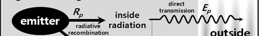


10 Surface-plasmon approach η = int R p R p + R nr η ' int = R p R p + R sp + R + R sp nr Surface Plasmons
11 The SP approach was started for organic LEDs ITO glass (anode) Organic molecules Cathode & Mirror SPP quenching (~40%) Conventional Structures: Strongly coupled to SPPs Main issue: SPP Radiation coupling Metallic mirror Metallic thin film SPP2 SPP1 SPP band gap ( Λ ~ π / ) k SPP Direct coupling ( Λ > π / k SPP ) SPP cross-coupling ( Λ = π /[ k k ]) SPP1 SPP2
12 Effect of SPP band gap on PL Angle resolved PL of dye molecule (DCM) 1 st and 2 nd order diffraction of SPPs Tracing 1 st order peaks shows SPP band gap.
13 Modification of Spontaneous Emission Rate of Eu 3+ Main emission of Eu 3+ (614nm) SPP quenching τ ( spacer thickness ) TRPL at 614nm
14 Self-driven dipole (CPS) modeling d p Metal interface 2 2 d d 2 e p + b0 p + ω0 p = E 2 dt dt m ω p = p e, E = E e i( ib/ 2) t i( ω ib/ 2) t 0 r 0 2 unknowns and 2 equations r 2 e b / b0 = 1 + Im{ E0 } mω p b b bb0 e Δ ω 8ω 4ω 2mω p Re{ E0 } 14


15 Dipole Decay Calculation Test : Metal Mirror Cavity pated pow wer dissi perpendicular dipole parallel dipole kx / k1 J. A. E. Wasey and W. L. Barnes, J. Mod. Opt. 47, ,

16 CPS Model Calculation for Spontaneous Emission Rates of an OLED Emission Spectrum No guided mode TM 0 TM 0 +TE 0 TM 0 +TE 0 +TM 1 70nm 100nm 200nm 390nm ra adiation rat te (R 0 ) total emission rate air emission emission to substrate guided modes emission to active layer guided modes active layer thickness (nm) dipole ( h = h + h ) cover (medium c) h c active material h (medium a) s a s c substrate (medium s)
17 Comparison with an experiment iency (% %) ratio (%) PL Effic Film Thickness (nm) power P air +P sub +1.0P guided P air +P sub +0.4P guided P air +P sub +0.8P guided P air +P sub +0.2P guided P air +P sub +0.6P guided P air +P sub +0.0P guided active layer thickness (μm) (measured) (calculated) 17
18 SPP Enhanced Spontaneous Emission of Eu 3+ Ion SE rate 90% SPP coupling 25 times SE rate Dipole-SPP coupling fraction Maximum internal efficiency
19 Role of Preferred Orientation of the Dipole Source Adv. Mater Angle integrated EL
20 Enhanced PL by Coupled SPP
21 Cross-Coupled vs Coupled SPP (1) (2) (3) (4)
 Half-processed (b)")
 (d) 250nm period (1 st order")
22 SPP Enhanced PL of InGaAs QW Most cited paper Un-processed (a) Half-processed (b) Fully-processed (c) 480nm period (2 nd order coupling) (d) 250nm period (1 st order coupling) (160nm gap)
23 1 st Result of SPP enhanced PL from InGaN QW Nature Materials, VOL 3, p , R = = f p E i ρ ( ω ) τ ( ω ) 2ε 0 E, ρ increase η external R = η extraction R + Rnr Nature Materials, VOL 3, p , 2004
24 1 st Result of SPP enhanced PL from InGaN QW Nature Materials, VOL 3, p , x100nm 2 133nm wide, 400nm period grating (no enhancement for 200nm wide, 600nm period grating) x2 x28 x Average internal quantum efficiency e cy estimation


25 TRPL of SPP enhanced InGaN QW emission
26 How does the surface-plasmon resonance contribute to emission rate? R = ( ) τω ( ) = 2 f p i ρ ω ε E 0 Field enhancement near the source layer High DOS due to decrease in group velocity emd Lab. Microoptics Lab Hanyang University 26
27 R = ( ) = f p i ρ ω τω ( ) 2 ε E 0 Field enhancement near the source layer High DOS due to decrease in group velocity Requirements for enhancing SE rate B -. slow group velocity -. tight confinement of mode -. low ohmic loss A -. large field enhancement fast group velocity, low loss slow group velocity, high loss A B Q.W. Q.W.
28 Purcell factor defining enhancement of the spontaneous emission F p R + R R = 1+ R R original additional additional original original For a cavity mode: F p Rcav 3 Q( λc / n) = = 2 R 4π V free 3 mode_ volume For a SP mode : F p R SP 1 λ k SP / k = 1+ = 1+ R 2 π L υ / c 0 SP 0 υ SP ( ( ωε ) dz ( z) dω E SP =, L = ω 2 dk E at dipole 2 We need a slow and confined mode!


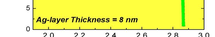
29 Factors influencing Purcell Enhancement F p (ω) GaN ~ ζ Ag ~ z Single Quantum Well GaN Variation with Ag thickness Variation with GaN thickness

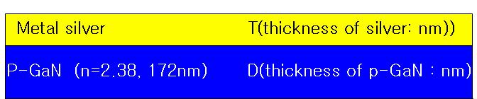
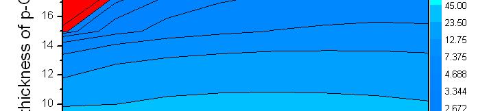


30 Purcell enhancement factor: A numerical factor (F-1) estimation cover Cover = 1.0 Cover = 1.5 Cover = 2.0 Need a very thin p-gan layer!!


31 Improvement I-L curve F p 2.68at10 K = 1.75at 300 K No improvement I-V curve the enhanced F p can be attributed to an increase in the spontaneous emission rate due to SP-QW coupling.
32 Why SP-LED hasn t been successful yet? Practical Barriers (especially for InGaN/GaN devices) Thin p-gan leads to abrupt occurrence of leakage current under a certain thickness SP propagation length in blue wavelength along the Ag/GaN interface is extremely short Nanopatterning becomes a huge burden at short wavelength Damageless p GaN patterning has been impossible Damageless p-gan patterning has been impossible SQW devices are prone to leakage current due to carrier overflow Silver is a nasty material with poor adhesion to GaN and tends to agglomerate at an elevated temperature
33 SP propagation length Nanopatterning of SPs [nm m] Propagat tion Length 1 PL SPs = 2 k k 3 2 ω ε mε d ε m = c ε m ε + d 2( ε m 2 ) Surface Plasmon on the Ag/GaN Interface Wavelength of Photon [nm] Green LEDs might be possible. Freq quency (2π πc/μm) Λ = λsp, 2λsp, 3λsp, 530nm λsp~140 nm 460nm λsp~70 nm SP-dispersion dspeso on Ag/GaN In-plane Wavevector (2π /μm) 2 nd order gratings (Λ~280nm) might be readily fabricated by Holo litho at Green.
34 Schematic structure Photon Sapphire n-gan Exciton generation Radiation InGaN MQW p-gan Metal (Ag-based) e-h Surface plasmon excitation Silicon submount Λ D h


35 High output directionality by grating with non-even fill-factor 1 st order grating, fill factor=0.1 1 st order grating, fill factor=0.5 2 nd order grating, fill factor=0.1 2 nd order grating, fill factor=0.7


36 Extraction efficiency of a metal grating Data sampling at λ = 530 nm / w = 5 nm η int 1+ ηext γ sp = 1 + γ γ nr sp 1+ ext sp η γ FDTD ηint = 1+ γ sp η ext 1 1 η ext η = FDTD int (1 + γ ) 1 γ sp sp γ nr η η γ int ext sp : nonradiative re-comb. rate : internal quantum eff. : extraction efficiency of metal grating : re-comb. rate to surface plasmon Max ~ 80% (at 140 nm / 40 nm)
 Λ = 250nm Grating depth = 50nm Gap to QW")


37 단일원기둥구조계산 Two-dimensional silver-grating (2 nd order) Λ = 250nm Grating depth = 50nm Gap to QW = 30 nm Normaliz zed LT / In nternal QE 1.2 Normalized LifeTime Internal Quantum Efficiency Upward Emitted Power Upward em mitted pow wer (a.u.) Diameter (nm) 169 nm
38 Optimum gap distance between metal and QW Upward enhanc cement λ = 530 nm d = 20 nm Distance [nm] coupling to lossy surface wave coupling to surface plasmons 6nm is a theoretical limit given by self-driven dipole (CPS) modeling [W. L. Barens and P. T. Worthing, Optics Communications 162, 16 (1999)]


39 Grating on p-gan Substrate mount Aperture Little damage to p-gan Enlarged surface area for low contact resistance Rotation o stage Linear stage X Z Y θ Mirro r L-Shape mount
 0.0045 0.004 0.0035 0.")


40 EL Measurement Power(a arb.) Higher output power up to 70 % ref 250A_3 250B_2 250C_2 270A_4 270B_2 270C_3 290A_ B_ Current(A)
41 Sample images


42 An Optimistic Estimation for SP-enhanced LEDs At green (530 nm) with a 1 st order grating MQW 5nm 10 nm grating de epth FDTD calculation l 20 nm 2.3 times more Photons generated 60 nm 140 nm 100 nm grating period 180 nm Good directionality Surface plasmon ed Ph hotons escap % 34.1% within 20 o after escape 1/(2n 2 ) = 8 % Wavelength (nm) (Bare-chip LED with 8 % extraction) (82 % / 8 %) x 2.3 ~ 24 times Brighter ( Optimized LED with 50 % extraction) (82 % / 50 %) x 2.3 ~ 4 times Brighter

43 Nanocavity lasers

44 Nanocavity lasers


 with a 1 st")
45 Key notes Final comments 1. How does the surface plamon resonance enhance the internal quantum efficiency of light source? 2. Understand the Fermi-Golden rule and Purcell enhancement factor in spontaneous emission 3. What are the practical difficulties in realizing SP-enhanced LEDs? 4. Summary of the five lectures External Efficiencies Conventional LED SP LED η ' = R p η = Ep R nr + R p ER + E R p p SP SP R + R + R nr p SP An Optimistic Estimation for SP-enhanced LEDs At green (530 nm) with a 1 st order grating MQW 5 nm 10 nm grating depth FDTD calculation 20 nm 2.3 times more Photons generation 60 nm 140 nm 100 nm grating period 180 nm
")

 Guided-mode")

 Surface-plasmon")
 Efficient")


46 Final comments Summary of the five lectures (06/23) Introduction: Micro- and nano-optics based on diffraction effect for next generation technologies (06/30) Guided-mode resonance (GMR) effect for filtering devices in LCD display panels (07/07) Surface-plasmons: A basic (07/14) Surface-plasmon waveguides for biosensor applications (07/21) Efficient light emission from LED, OLED, and nanolasers by surface-plasmon resonance R 0 T 0 GMR grating Micros D cor e metal strip SPP mode cladding core metal slab cladding
47 Final comments Summary of the five lectures Now, let s get back to Macros with Nanos and Micros.
Efficient light emission from LEDs, OLEDs, and nanolasers via surface-plasmon resonance
 Efficient light emission from LEDs, OLEDs, and nanolasers via surface-plasmon resonance Seok Ho Song, Hanyang University, http://optics.anyang.ac.kr/~shsong silver grating Key notes 1. How does the surface
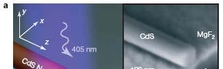
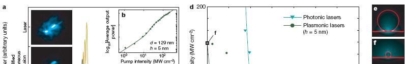
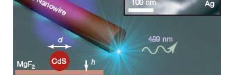
Enhancing the Rate of Spontaneous Emission in Active Core-Shell Nanowire Resonators
 Chapter 6 Enhancing the Rate of Spontaneous Emission in Active Core-Shell Nanowire Resonators 6.1 Introduction Researchers have devoted considerable effort to enhancing light emission from semiconductors
Enhancement of Light Extraction Efficiency in Organic Light Emitting Device with Multi-Stacked Cathode and High Refractive Index Anode
 Enhancement of Light Extraction Efficiency in Organic Light Emitting Device with Multi-Stacked Cathode and High Refractive Index Anode Kanazawa Institute of Technology, Jaan Akiyoshi Mikami and Takao Goto
Ultrafast single photon emitting quantum photonic structures. based on a nano-obelisk
 Ultrafast single photon emitting quantum photonic structures based on a nano-obelisk Je-Hyung Kim, Young-Ho Ko, Su-Hyun Gong, Suk-Min Ko, Yong-Hoon Cho Department of Physics, Graduate School of Nanoscience
Understanding Nanoplasmonics. Greg Sun University of Massachusetts Boston
 Understanding Nanoplasmonics Greg Sun University of Massachusetts Boston Nanoplasmonics Space 100pm 1nm 10nm 100nm 1μm 10μm 100μm 1ns 100ps 10ps Photonics 1ps 100fs 10fs 1fs Time Surface Plasmons Surface
Light Extraction in OLED with Corrugated Substrates Franky So
 Light Extraction in OLED with Corrugated Substrates Franky So Department of Materials Science and Engineering North Carolina State University Raleigh, NC 27695-7907 1 Where Did the Light Go? Modes Distribution
Photonic Micro and Nanoresonators
 Photonic Micro and Nanoresonators Hauptseminar Nanooptics and Nanophotonics IHFG Stuttgart Overview 2 I. Motivation II. Cavity properties and species III. Physics in coupled systems Cavity QED Strong and
Radiation-matter interaction.
 Radiation-matter interaction Radiation-matter interaction Classical dipoles Dipole radiation Power radiated by a classical dipole in an inhomogeneous environment The local density of optical states (LDOS)
Lecture 10 Light-Matter Interaction Part 4 Surface Polaritons 2. EECS Winter 2006 Nanophotonics and Nano-scale Fabrication P.C.
 Lecture 10 Light-Matter Interaction Part 4 Surface Polaritons 2 EECS 598-002 Winter 2006 Nanophotonics and Nano-scale Fabrication P.C.Ku Schedule for the rest of the semester Introduction to light-matter
ECE 240a - Notes on Spontaneous Emission within a Cavity
 ECE 0a - Notes on Spontaneous Emission within a Cavity Introduction Many treatments of lasers treat the rate of spontaneous emission as specified by the time constant τ sp as a constant that is independent
Wednesday 3 September Session 3: Metamaterials Theory (16:15 16:45, Huxley LT308)
") Session 3: Metamaterials Theory (16:15 16:45, Huxley LT308) (invited) TBC Session 3: Metamaterials Theory (16:45 17:00, Huxley LT308) Light trapping states in media with longitudinal electric waves D McArthur,
Session 3: Metamaterials Theory (16:15 16:45, Huxley LT308) (invited) TBC Session 3: Metamaterials Theory (16:45 17:00, Huxley LT308) Light trapping states in media with longitudinal electric waves D McArthur,
Supporting Information
 Supporting Information Light emission near a gradient metasurface Leonard C. Kogos and Roberto Paiella Department of Electrical and Computer Engineering and Photonics Center, Boston University, Boston,
Supplementary Information for
 Supplementary Information for Multi-quantum well nanowire heterostructures for wavelength-controlled lasers Fang Qian 1, Yat Li 1 *, Silvija Gradečak 1, Hong-Gyu Park 1, Yajie Dong 1, Yong Ding 2, Zhong
Origin of Optical Enhancement by Metal Nanoparticles. Greg Sun University of Massachusetts Boston
 Origin of Optical Enhancement by Metal Nanoparticles Greg Sun University of Massachusetts Boston Nanoplasmonics Space 100pm 1nm 10nm 100nm 1μm 10μm 100μm Photonics 1ns 100ps 10ps 1ps 100fs 10fs 1fs Time
Surface plasmon waveguides
 Surface plasmon waveguides Introduction Size Mismatch between Scaled CMOS Electronics and Planar Photonics Photonic integrated system with subwavelength scale components CMOS transistor: Medium-sized molecule
Signal regeneration - optical amplifiers
 Signal regeneration - optical amplifiers In any atom or solid, the state of the electrons can change by: 1) Stimulated absorption - in the presence of a light wave, a photon is absorbed, the electron is
Plasmonic Photovoltaics Harry A. Atwater California Institute of Technology
 Plasmonic Photovoltaics Harry A. Atwater California Institute of Technology Surface plasmon polaritons and localized surface plasmons Plasmon propagation and absorption at metal-semiconductor interfaces
Thermal Emission in the Near Field from Polar Semiconductors and the Prospects for Energy Conversion
 Thermal Emission in the Near Field from Polar Semiconductors and the Prospects for Energy Conversion R.J. Trew, K.W. Kim, V. Sokolov, and B.D Kong Electrical and Computer Engineering North Carolina State
Photonic Crystal Nanocavities for Efficient Light Confinement and Emission
 Journal of the Korean Physical Society, Vol. 42, No., February 2003, pp. 768 773 Photonic Crystal Nanocavities for Efficient Light Confinement and Emission Axel Scherer, T. Yoshie, M. Lončar, J. Vučković
Laser Basics. What happens when light (or photon) interact with a matter? Assume photon energy is compatible with energy transition levels.
 interact with a matter? Assume photon energy is compatible with energy transition levels.") What happens when light (or photon) interact with a matter? Assume photon energy is compatible with energy transition levels. Electron energy levels in an hydrogen atom n=5 n=4 - + n=3 n=2 13.6 = [ev]
What happens when light (or photon) interact with a matter? Assume photon energy is compatible with energy transition levels. Electron energy levels in an hydrogen atom n=5 n=4 - + n=3 n=2 13.6 = [ev]
Influence of the quantum well models on the numerical simulation of planar InGaN/GaN LED results
 Journal of Physics: Conference Series PAPER OPEN ACCESS Influence of the quantum well models on the numerical simulation of planar InGaN/GaN LED results To cite this article: J Podgórski et al 2016 J.
(b) Spontaneous emission. Absorption, spontaneous (random photon) emission and stimulated emission.
 Spontaneous emission. Absorption, spontaneous (random photon) emission and stimulated emission.") Lecture 10 Stimulated Emission Devices Lasers Stimulated emission and light amplification Einstein coefficients Optical fiber amplifiers Gas laser and He-Ne Laser The output spectrum of a gas laser Laser
Lecture 10 Stimulated Emission Devices Lasers Stimulated emission and light amplification Einstein coefficients Optical fiber amplifiers Gas laser and He-Ne Laser The output spectrum of a gas laser Laser
Determining the orientation of the emissive dipole moment associated with dye molecules in microcavity structures
 journal of modern optics, 15 october 2004 vol. 51, no. 15, 2287 2295 Determining the orientation of the emissive dipole moment associated with dye molecules in microcavity structures S. H. GARRETT, J.
Carrier Loss Analysis for Ultraviolet Light-Emitting Diodes
 Carrier Loss Analysis for Ultraviolet Light-Emitting Diodes Joachim Piprek, Thomas Katona, Stacia Keller, Steve DenBaars, and Shuji Nakamura Solid State Lighting and Display Center University of California
Emission Spectra of the typical DH laser
 Emission Spectra of the typical DH laser Emission spectra of a perfect laser above the threshold, the laser may approach near-perfect monochromatic emission with a spectra width in the order of 1 to 10
Entangled Photon Generation via Biexciton in a Thin Film
 Entangled Photon Generation via Biexciton in a Thin Film Hiroshi Ajiki Tokyo Denki University 24,Apr. 2017 Emerging Topics in Optics (IMA, Univ. Minnesota) Entangled Photon Generation Two-photon cascade
Optical Investigation of the Localization Effect in the Quantum Well Structures
 Department of Physics Shahrood University of Technology Optical Investigation of the Localization Effect in the Quantum Well Structures Hamid Haratizadeh hamid.haratizadeh@gmail.com IPM, SCHOOL OF PHYSICS,
Computer Aided Design of GaN Light-Emitting Diodes. Copyright 2006 Crosslight Software Inc.
 Computer Aided Design of GaN Light-Emitting Diodes Copyright 2006 Crosslight Software Inc. www.crosslight.com 1 2 Contents Available tools and modules. Simulation of IQE droop. Design of superlattice.
Quantum Optics in Wavelength Scale Structures
 Quantum Optics in Wavelength Scale Structures SFB Summer School Blaubeuren July 2012 J. G. Rarity University of Bristol john.rarity@bristol.ac.uk Confining light: periodic dielectric structures Photonic
Introduction. Chapter Optics at the Nanoscale
 Chapter 1 Introduction 1.1 Optics at the Nanoscale The interaction of light with matter is one of the most significant processes on the planet, forming the basis of some of the most famous scientific discoveries
Light Interaction with Small Structures
 Light Interaction with Small Structures Molecules Light scattering due to harmonically driven dipole oscillator Nanoparticles Insulators Rayleigh Scattering (blue sky) Semiconductors...Resonance absorption
Supporting information. Unidirectional Doubly Enhanced MoS 2 Emission via
 Supporting information Unidirectional Doubly Enhanced MoS 2 Emission via Photonic Fano Resonances Xingwang Zhang, Shinhyuk Choi, Dake Wang, Carl H. Naylor, A. T. Charlie Johnson, and Ertugrul Cubukcu,,*
Quantum and Non-local Transport Models in Crosslight Device Simulators. Copyright 2008 Crosslight Software Inc.
 Quantum and Non-local Transport Models in Crosslight Device Simulators Copyright 2008 Crosslight Software Inc. 1 Introduction Quantization effects Content Self-consistent charge-potential profile. Space
Nanophysics: Main trends
 Nano-opto-electronics Nanophysics: Main trends Nanomechanics Main issues Light interaction with small structures Molecules Nanoparticles (semiconductor and metallic) Microparticles Photonic crystals Nanoplasmonics
High Power Diode Lasers
 Lecture 10/1 High Power Diode Lasers Low Power Lasers (below tenth of mw) - Laser as a telecom transmitter; - Laser as a spectroscopic sensor; - Laser as a medical diagnostic tool; - Laser as a write-read
II Theory Of Surface Plasmon Resonance (SPR)
") II Theory Of Surface Plasmon Resonance (SPR) II.1 Maxwell equations and dielectric constant of metals Surface Plasmons Polaritons (SPP) exist at the interface of a dielectric and a metal whose electrons
II Theory Of Surface Plasmon Resonance (SPR) II.1 Maxwell equations and dielectric constant of metals Surface Plasmons Polaritons (SPP) exist at the interface of a dielectric and a metal whose electrons
Stimulated Emission Devices: LASERS
 Stimulated Emission Devices: LASERS 1. Stimulated Emission and Photon Amplification E 2 E 2 E 2 hυ hυ hυ In hυ Out hυ E 1 E 1 E 1 (a) Absorption (b) Spontaneous emission (c) Stimulated emission The Principle
Introduction to optical waveguide modes
 Chap. Introduction to optical waveguide modes PHILIPPE LALANNE (IOGS nd année) Chapter Introduction to optical waveguide modes The optical waveguide is the fundamental element that interconnects the various
GaN-based Devices: Physics and Simulation
 GaN-based Devices: Physics and Simulation Joachim Piprek NUSOD Institute Collaborators Prof. Shuji Nakamura, UCSB Prof. Steve DenBaars, UCSB Dr. Stacia Keller, UCSB Dr. Tom Katona, now at S-ET Inc. Dr.
Last Lecture. Overview and Introduction. 1. Basic optics and spectroscopy. 2. Lasers. 3. Ultrafast lasers and nonlinear optics
 Last Lecture Overview and Introduction 1. Basic optics and spectroscopy. Lasers 3. Ultrafast lasers and nonlinear optics 4. Time-resolved spectroscopy techniques Jigang Wang, Feb, 009 Today 1. Spectroscopy
Surface-Plasmon Sensors
 Surface-Plasmon Sensors Seok Ho Song Physics Department in Hanyang University Dongho Shin, Jaewoong Yun, Kihyong Choi Gwansu Lee, Samsung Electro-Mechanics Contents Dispersion relation of surface plasmons
Plasmonic nanoguides and circuits
 Plasmonic nanoguides and circuits Introduction: need for plasmonics? Strip SPPs Cylindrical SPPs Gap SPP waveguides Channel plasmon polaritons Dielectric-loaded SPP waveguides PLASMOCOM 1. Intro: need
Single Emitter Detection with Fluorescence and Extinction Spectroscopy
 Single Emitter Detection with Fluorescence and Extinction Spectroscopy Michael Krall Elements of Nanophotonics Associated Seminar Recent Progress in Nanooptics & Photonics May 07, 2009 Outline Single molecule
Surface Plasmon Enhanced Light-Emitting Diode
 IEEE JOURNAL OF QUANTUM ELECTRONICS, VOL. 36, NO. 10, OCTOBER 2000 1131 Surface Plasmon Enhanced Light-Emitting Diode Jelena Vučković, Marko Lončar, and Axel Scherer Abstract A method for enhancing the
Quantum Information Processing with Electrons?
 Quantum Information Processing with 10 10 Electrons? René Stock IQIS Seminar, October 2005 People: Barry Sanders Peter Marlin Jeremie Choquette Motivation Quantum information processing realiations Ions
Lecture 10: Surface Plasmon Excitation. 5 nm
 Excitation Lecture 10: Surface Plasmon Excitation 5 nm Summary The dispersion relation for surface plasmons Useful for describing plasmon excitation & propagation This lecture: p sp Coupling light to surface
Making OLEDs efficient
 Making OLEDs efficient cathode anode light-emitting layer η = γ EL r ηpl k st External Efficiency Outcoupling Internal efficiency of LEDs η = γ EL r ηpl k st γ = excitons formed per charge flowing in the
ECE 484 Semiconductor Lasers
 ECE 484 Semiconductor Lasers Dr. Lukas Chrostowski Department of Electrical and Computer Engineering University of British Columbia January, 2013 Module Learning Objectives: Understand the importance of
2008,, Jan 7 All-Paid US-Japan Winter School on New Functionalities in Glass. Controlling Light with Nonlinear Optical Glasses and Plasmonic Glasses
 2008,, Jan 7 All-Paid US-Japan Winter School on New Functionalities in Glass Photonic Glass Controlling Light with Nonlinear Optical Glasses and Plasmonic Glasses Takumi FUJIWARA Tohoku University Department
Chapter 2 Optical Transitions
 Chapter 2 Optical Transitions 2.1 Introduction Among energy states, the state with the lowest energy is most stable. Therefore, the electrons in semiconductors tend to stay in low energy states. If they
4. Integrated Photonics. (or optoelectronics on a flatland)
") 4. Integrated Photonics (or optoelectronics on a flatland) 1 x Benefits of integration in Electronics: Are we experiencing a similar transformation in Photonics? Mach-Zehnder modulator made from Indium
4. Integrated Photonics (or optoelectronics on a flatland) 1 x Benefits of integration in Electronics: Are we experiencing a similar transformation in Photonics? Mach-Zehnder modulator made from Indium
InGaAs-AlAsSb quantum cascade lasers
 InGaAs-AlAsSb quantum cascade lasers D.G.Revin, L.R.Wilson, E.A.Zibik, R.P.Green, J.W.Cockburn Department of Physics and Astronomy, University of Sheffield, UK M.J.Steer, R.J.Airey EPSRC National Centre
Theory of Photonic Crystal Slabs by the Guided-Mode Expansion Method
 Theory of Photonic Crystal Slabs by the Guided-Mode Expansion Method Dario Gerace* Lucio Claudio Andreani Dipartimento di Fisica Alessandro Volta, Università degli Studi di Pavia, Pavia (Italy) *Quantum
Simulation of Optical Modes in Microcavities
 Simulation of Optical Modes in Microcavities Bernd Witzigmann, Matthias Streiff Computational Optoelectronics Group Integrated Systems Laboratory, ETH Zurich bernd@iis.ee.ethz.ch Overview Introduction
Nanoscale Systems for Opto-Electronics
 Nanoscale Systems for Opto-Electronics 675 PL intensity [arb. units] 700 Wavelength [nm] 650 625 600 5µm 1.80 1.85 1.90 1.95 Energy [ev] 2.00 2.05 Nanoscale Systems for Opto-Electronics Lecture 1 Dozent:
Photonic devices for quantum information processing:
 Outline Photonic devices for quantum information processing: coupling to dots, structure design and fabrication Optoelectronics Group, Cavendish Lab Outline Vuckovic s group Noda s group Outline Outline
Nano-antenne plasmonique pour l'émission de photons uniques
 Nano-antenne plasmonique pour l'émission de photons uniques JJ Greffet LCF, Institut d Optique, Institut Universitaire de France This work has been supported by the Agence Nationale de la Recherche, RTRA
Chapter 5. Semiconductor Laser
 Chapter 5 Semiconductor Laser 5.0 Introduction Laser is an acronym for light amplification by stimulated emission of radiation. Albert Einstein in 1917 showed that the process of stimulated emission must
External (differential) quantum efficiency Number of additional photons emitted / number of additional electrons injected
 quantum efficiency Number of additional photons emitted / number of additional electrons injected") Semiconductor Lasers Comparison with LEDs The light emitted by a laser is generally more directional, more intense and has a narrower frequency distribution than light from an LED. The external efficiency
Semiconductor Lasers Comparison with LEDs The light emitted by a laser is generally more directional, more intense and has a narrower frequency distribution than light from an LED. The external efficiency
Single Semiconductor Nanostructures for Quantum Photonics Applications: A solid-state cavity-qed system with semiconductor quantum dots
 The 3 rd GCOE Symposium 2/17-19, 19, 2011 Tohoku University, Sendai, Japan Single Semiconductor Nanostructures for Quantum Photonics Applications: A solid-state cavity-qed system with semiconductor quantum
SURFACE PLASMONS AND THEIR APPLICATIONS IN ELECTRO-OPTICAL DEVICES
 SURFACE PLASMONS AND THEIR APPLICATIONS IN ELECTRO-OPTICAL DEVICES Igor Zozouleno Solid State Electronics Department of Science and Technology Linöping University Sweden igozo@itn.liu.se http://www.itn.liu.se/meso-phot
Defect-based Photonic Crystal Cavity for Silicon Laser
 Defect-based Photonic Crystal Cavity for Silicon Laser Final Term Paper for Nonlinear Optics PHYC/ECE 568 Arezou Khoshakhlagh Instructor: Prof. M. Sheikh-Bahae University of New Mexico karezou@unm.edu
Photonics applications II. Ion-doped ChGs
 Photonics applications II Ion-doped ChGs 1 ChG as a host for doping; pros and cons - Important - Condensed summary Low phonon energy; Enabling emission at longer wavelengths Reduced nonradiative multiphonon
Photoluminescence emission through thin metal films via coupled surface plasmon polaritons
 Journal of Modern Optics Vol. 52, No. 6, 15 April 2005, 833 843 Photoluminescence emission through thin metal films via coupled surface plasmon polaritons S. WEDGE*y, S. H. GARRETTy, I. SAGEz and W. L.
Quantum Optics exam. M2 LOM and Nanophysique. 28 November 2017
 Quantum Optics exam M LOM and Nanophysique 8 November 017 Allowed documents : lecture notes and problem sets. Calculators allowed. Aux francophones (et francographes) : vous pouvez répondre en français.
Photonic Crystals: Periodic Surprises in Electromagnetism. You can leave home without them. Complete Band Gaps: Steven G.
 Photonic Crystals: Periodic Surprises in lectromagnetism Steven G. ohnson MIT Complete Band Gaps: You can leave home without them. How else can we confine light? Total Internal Reflection n o n i > n o
PHYSICS nd TERM Outline Notes (continued)
") PHYSICS 2800 2 nd TERM Outline Notes (continued) Section 6. Optical Properties (see also textbook, chapter 15) This section will be concerned with how electromagnetic radiation (visible light, in particular)
PHYSICS 2800 2 nd TERM Outline Notes (continued) Section 6. Optical Properties (see also textbook, chapter 15) This section will be concerned with how electromagnetic radiation (visible light, in particular)
Photonic crystals. Semi-conductor crystals for light. The smallest dielectric lossless structures to control whereto and how fast light flows
 Photonic crystals Semi-conductor crystals for light The smallest dielectric lossless structures to control whereto and how fast light flows Femius Koenderink Center for Nanophotonics AMOLF, Amsterdam f.koenderink@amolf.nl
Polariton laser in micropillar cavities
 Polariton laser in micropillar cavities D. Bajoni, E. Wertz, P. Senellart, I. Sagnes, S. Bouchoule, A. Miard, E. Semenova, A. Lemaître and J. Bloch Laboratoire de Photonique et de Nanostructures LPN/CNRS,
Spring 2009 EE 710: Nanoscience and Engineering
 Spring 009 EE 710: Nanoscience and Engineering Part 10: Surface Plasmons in Metals Images and figures supplied from Hornyak, Dutta, Tibbals, and Rao, Introduction to Nanoscience, CRC Press Boca Raton,
Nanomaterials and their Optical Applications
 Nanomaterials and their Optical Applications Winter Semester 2013 Lecture 02 rachel.grange@uni-jena.de http://www.iap.uni-jena.de/multiphoton Lecture 2: outline 2 Introduction to Nanophotonics Theoretical
Organic LEDs part 6. Exciton Recombination Region in Organic LEDs. Handout: Bulovic, et al., Chem. Phys. Lett. 287, 455 (1998); 308, 317 (1999).
; 308, 317 (1999).") Organic LEDs part 6 Exciton Recombination Region in Organic LEDs White OLED Flexible OLEDs Solvation Effect Solid State Solvation Handout: Bulovic, et al., Chem. Phys. Lett. 287, 455 (1998); 308, 317 (1999).
Organic LEDs part 6 Exciton Recombination Region in Organic LEDs White OLED Flexible OLEDs Solvation Effect Solid State Solvation Handout: Bulovic, et al., Chem. Phys. Lett. 287, 455 (1998); 308, 317 (1999).
Laser Diodes. Revised: 3/14/14 14: , Henry Zmuda Set 6a Laser Diodes 1
 Laser Diodes Revised: 3/14/14 14:03 2014, Henry Zmuda Set 6a Laser Diodes 1 Semiconductor Lasers The simplest laser of all. 2014, Henry Zmuda Set 6a Laser Diodes 2 Semiconductor Lasers 1. Homojunction
Lecture 0. NC State University
 Chemistry 736 Lecture 0 Overview NC State University Overview of Spectroscopy Electronic states and energies Transitions between states Absorption and emission Electronic spectroscopy Instrumentation Concepts
Photonics Beyond Diffraction Limit:
 Photonics Beyond Diffraction Limit: Plasmon Cavity, Waveguide and Lasers Xiang Zhang University of California, Berkeley Light-Matter Interaction: Electrons and Photons Photons Visible / IR ~ 1 m Electrons
Surface Plasmon Amplification by Stimulated Emission of Radiation. By: Jonathan Massey-Allard Graham Zell Justin Lau
 Surface Plasmon Amplification by Stimulated Emission of Radiation By: Jonathan Massey-Allard Graham Zell Justin Lau Surface Plasmons (SPs) Quanta of electron oscillations in a plasma. o Electron gas in
Simulation of GaN-based Light-Emitting Devices
 Simulation of GaN-based Light-Emitting Devices Joachim Piprek Solid-State Lighting and Display Center Materials Department, College of Engineering University of California, Santa Barbara, CA 93106 piprek@ieee.org
Model Answer (Paper code: AR-7112) M. Sc. (Physics) IV Semester Paper I: Laser Physics and Spectroscopy
 M. Sc. (Physics) IV Semester Paper I: Laser Physics and Spectroscopy") Model Answer (Paper code: AR-7112) M. Sc. (Physics) IV Semester Paper I: Laser Physics and Spectroscopy Section I Q1. Answer (i) (b) (ii) (d) (iii) (c) (iv) (c) (v) (a) (vi) (b) (vii) (b) (viii) (a) (ix)
Model Answer (Paper code: AR-7112) M. Sc. (Physics) IV Semester Paper I: Laser Physics and Spectroscopy Section I Q1. Answer (i) (b) (ii) (d) (iii) (c) (iv) (c) (v) (a) (vi) (b) (vii) (b) (viii) (a) (ix)
Quantum Optics in Photonic Crystals. Peter Lodahl Dept. of Communications, Optics & Materials (COM) Technical University of Denmark
 Technical University of Denmark") Quantum Optics in Photonic Crystals Peter Lodahl Dept. of Communications, Optics & Materials (COM) Technical University of Denmark Acknowledgements AMOLF Institute Amsterdam / University of Twente Ivan
Quantum Optics in Photonic Crystals Peter Lodahl Dept. of Communications, Optics & Materials (COM) Technical University of Denmark Acknowledgements AMOLF Institute Amsterdam / University of Twente Ivan
Surface Plasmon Enhanced Light Emitting Devices
 Surface Plasmon Enhanced Light Emitting Devices Alexander Mikhailovsky, Jacek Ostrowski, Hadjar Benmansour, and Guillermo Bazan + Department of Chemistry and Biochemistry, University of California Santa
Energy transport in metal nanoparticle plasmon waveguides
 Energy transport in metal nanoparticle plasmon waveguides Stefan A. Maier, Pieter G. Kik, and Harry A. Atwater California Institute of Technology Thomas J. Watson Laboratory of Applied Physics, Pasadena,
Appendix. Photonic crystal lasers: future integrated devices
 91 Appendix Photonic crystal lasers: future integrated devices 5.1 Introduction The technology of photonic crystals has produced a large variety of new devices. However, photonic crystals have not been
The Study of Cavitation Bubble- Surface Plasmon Resonance Interaction For LENR and Biochemical processes
 The Study of Cavitation Bubble- Surface Plasmon Resonance Interaction For LENR and Biochemical processes Farzan Amini fnamini@aol.com ABSTRACT The cavitation bubble resonator (CBR) can be used as a new
OPTI510R: Photonics. Khanh Kieu College of Optical Sciences, University of Arizona Meinel building R.626
 OPTI510R: Photonics Khanh Kieu College of Optical Sciences, University of Arizona kkieu@optics.arizona.edu Meinel building R.626 Announcements HW#3 is assigned due Feb. 20 st Mid-term exam Feb 27, 2PM
Lecture 14 Dispersion engineering part 1 - Introduction. EECS Winter 2006 Nanophotonics and Nano-scale Fabrication P.C.Ku
 Lecture 14 Dispersion engineering part 1 - Introduction EEC 598-2 Winter 26 Nanophotonics and Nano-scale Fabrication P.C.Ku chedule for the rest of the semester Introduction to light-matter interaction
Optimizing the performance of metal-semiconductor-metal photodetectors by embedding nanoparticles in the absorption layer
 Journal of Electrical and Electronic Engineering 2015; 3(2-1): 78-82 Published online February 10, 2015 (http://www.sciencepublishinggroup.com/j/jeee) doi: 10.11648/j.jeee.s.2015030201.27 ISSN: 2329-1613
Study on Quantum Dot Lasers and their advantages
 Study on Quantum Dot Lasers and their advantages Tae Woo Kim Electrical and Computer Engineering University of Illinois, Urbana Champaign Abstract Basic ideas for understanding a Quantum Dot Laser were
Lecture 7 Light-Matter Interaction Part 1 Basic excitation and coupling. EECS Winter 2006 Nanophotonics and Nano-scale Fabrication P.C.
 Lecture 7 Light-Matter Interaction Part 1 Basic excitation and coupling EECS 598-00 Winter 006 Nanophotonics and Nano-scale Fabrication P.C.Ku What we have learned? Nanophotonics studies the interaction
Fabrication of Efficient Blue Light-Emitting Diodes with InGaN/GaN Triangular Multiple Quantum Wells. Abstract
 Fabrication of Efficient Blue Light-Emitting Diodes with InGaN/GaN Triangular Multiple Quantum Wells R. J. Choi, H. W. Shim 2, E. K. Suh 2, H. J. Lee 2, and Y. B. Hahn,2, *. School of Chemical Engineering
Optical Properties of Lattice Vibrations
 Optical Properties of Lattice Vibrations For a collection of classical charged Simple Harmonic Oscillators, the dielectric function is given by: Where N i is the number of oscillators with frequency ω
Electromagnetic Wave Propagation Lecture 13: Oblique incidence II
 Electromagnetic Wave Propagation Lecture 13: Oblique incidence II Daniel Sjöberg Department of Electrical and Information Technology October 2016 Outline 1 Surface plasmons 2 Snel s law in negative-index
Nanomaterials and their Optical Applications
 Nanomaterials and their Optical Applications Winter Semester 2012 Lecture 08 rachel.grange@uni-jena.de http://www.iap.uni-jena.de/multiphoton Outline: Photonic crystals 2 1. Photonic crystals vs electronic
independent quantities. The Purcell factor presented in Eq. (1) can be more generally defined as: F = R sp,cav R bulk (2)
 can be more generally defined as: F = R sp,cav R bulk (2)") 1 Purcell Effect in the Stimulated and Spontaneous Emission Rates of Nanoscale Semiconductor Lasers Bruno Romeira and Andrea Fiore arxiv:1801.08879v1 [physics.optics] 6 Jan 018 Abstract Nanoscale semiconductor
1 Purcell Effect in the Stimulated and Spontaneous Emission Rates of Nanoscale Semiconductor Lasers Bruno Romeira and Andrea Fiore arxiv:1801.08879v1 [physics.optics] 6 Jan 018 Abstract Nanoscale semiconductor
Diode Lasers and Photonic Integrated Circuits
 Diode Lasers and Photonic Integrated Circuits L. A. COLDREN S. W. CORZINE University of California Santa Barbara, California A WILEY-INTERSCIENCE PUBLICATION JOHN WILEY & SONS, INC. NEW YORK / CHICHESTER
Broadband Subwavelength Imaging with a Wire Medium Slab Loaded with Graphene Sheets
 Broadband Subwavelength Imaging with a Wire Medium Slab Loaded with Graphene Sheets Ali Forouzmand and Alexander B. Yakovlev Center for Applied Electromagnetic Systems Research (CAESR) Department of Electrical
Three-Dimensional Silicon-Germanium Nanostructures for Light Emitters and On-Chip Optical. Interconnects
 Three-Dimensional Silicon-Germanium Nanostructures for Light Emitters and On-Chip Optical eptember 2011 Interconnects Leonid Tsybeskov Department of Electrical and Computer Engineering New Jersey Institute
Quantum Optics with Mesoscopic Systems II
 Quantum Optics with Mesoscopic Systems II A. Imamoglu Quantum Photonics Group, Department of Physics ETH-Zürich Outline 1) Cavity-QED with a single quantum dot 2) Optical pumping of quantum dot spins 3)
Semiconductor Lasers for Optical Communication
 Semiconductor Lasers for Optical Communication Claudio Coriasso Manager claudio.coriasso@avagotech.com Turin Technology Centre 10Gb/s DFB Laser MQW 1 Outline 1) Background and Motivation Communication
Luminescence. Photoluminescence (PL) is luminescence that results from optically exciting a sample.
 is luminescence that results from optically exciting a sample.") Luminescence Topics Radiative transitions between electronic states Absorption and Light emission (spontaneous, stimulated) Excitons (singlets and triplets) Franck-Condon shift(stokes shift) and vibrational
Luminescence Topics Radiative transitions between electronic states Absorption and Light emission (spontaneous, stimulated) Excitons (singlets and triplets) Franck-Condon shift(stokes shift) and vibrational
Mar Yunsu Sung. Yunsu Sung. Special Topics in Optical Engineering II(15/1)
") Mar 12 2015 Contents Two-port model Rate equation and damping Small signal response Conclusion Two Port Model I:Current V:Voltage P: Optical Power ν: Optical frequency shift Model summarize parasitic effects
Mar 12 2015 Contents Two-port model Rate equation and damping Small signal response Conclusion Two Port Model I:Current V:Voltage P: Optical Power ν: Optical frequency shift Model summarize parasitic effects