Photonics Beyond Diffraction Limit:
|
|
|
- Francis Parks
- 6 years ago
- Views:
Transcription
1 Photonics Beyond Diffraction Limit: Plasmon Cavity, Waveguide and Lasers Xiang Zhang University of California, Berkeley


2 Light-Matter Interaction: Electrons and Photons Photons Visible / IR ~ 1 m Electrons e ~ 1 nm Quantum dot Not efficient Interaction NV center 5 nm 0.36 nm


3 Challenges in Scaling Down of Photonics Intel The Photonic Chip M. Paniccia Intel Corp., Silicon Photonics (2005) Key Issues: Nanoscale Waveguides On Chip Light Source Ultrafast Modulation New approaes Hybrid Plasmon Waveguide Plasmon Nano Lasers Graphene, Plasmon Modulators
4 Outline Indefinite Nano Cavity Deep Sub Plasmon Waveguide and Lasers
5 Optical Fabry-Perot Cavity m=1 m=2 m=3 mirror mirror Resonance frequency m f m 2L c n c : speed of light in vacuum L : cavity size m: mode order (1, 2, 3, ) University of California, Berkeley 5
 University of California,")
6 Quality factor Q and modal volume V Cavity mode mirror mirror Quality factor Q Q 2 Electromagnetic Energy Energy Dissipated per Stored cycle Modal Volume V Q/V Figure of Merit V Total Electromagnetic Energy max( Electromagnetic Energy Density) University of California, Berkeley 6
![V [(λ) 3 ] 10 3 10 2 10 1 10-2 Subwavelength confinement Optical Micro- and Nano-cavities Plasmonic](/docs-images/78/77430581/images/7-0.jpg "Fabry-Perot (V. Sorger et al) Plasmonic microdisk (B.")
 3 Q/V~ 1,500(/n) -3 Photonic crystal (S. Noda et al) Q ~ 2.510 6 V ~ 1.")
; D. K. Armani et al.")
 optical nonlinearities: Q 2")
 3 Q/V~100,000 () -3 V ~ 0.04 () 3 Q/V~5000 () -3 O. Painter et al., Opt. Exp.")
; V. Sorger et al, Nano Lett., 9 3489 (2009).")
7 V [(λ) 3 ] Subwavelength confinement Optical Micro- and Nano-cavities Plasmonic Fabry-Perot (V. Sorger et al) Plasmonic microdisk (B. Min et al) Q ~ 1,400 V ~ 6 () 3 Q/V~230 () -3 Microring resonator (M. Lipson et al) Q ~ V ~ 10(/n) 3 Q/V~ 1,500(/n) -3 Photonic crystal (S. Noda et al) Q ~ V ~ 1.4 (/n) 3 Q/V~1.8x10 6 (/n) -3 High Q 10-4 Q ~ 200 scale bar: 2 μm 100 nm Ref.: K. Vahala, Nature 424, 839 (2003); D. K. Armani et al., Nature 421, 925 (2003); 10-6 Enhancement of light-matter interactions: - Purcell factor for spontaneous emission: Q/V - Strong coupling for cavity QED: Q/V 1/2 - (3) optical nonlinearities: Q 2 /V - Optical forces and trapping: Q/V - Bio-sensing: Q/V Indefinite metamaterial nanocavity Q ~ 20 V ~ () 3 Q/V~100,000 () -3 V ~ 0.04 () 3 Q/V~5000 () -3 O. Painter et al., Opt. Exp. 13, 1515 (2005); M. Lipson et al., Nature 435, 325 (2005); S. Noda et al., Nature 425, 944 (2003); B. Min et al, Nature 457, 455 (2009); V. Sorger et al, Nano Lett., (2009) Microtoroid Microsphere 25 um 50 um (K. Vahala et al) Q ~ V ~ 2000(/n) 3 Q/V ~ 5x10 6 (/n) -3 Q University of California, Berkeley 7
![V [(λ) 3 ] 10 3 10 2 10 Q/V in Optical Cavities](/docs-images/78/77430581/images/8-0.jpg "Enhancement of light-matter interactions: -")
")

 Q ~ 1.")

 Q ~ 10 8 10 10 V ~ 2000(/n) 3 Q/V ~")

 -3 scale bar: 2 μm (B. Min et al) (S.")
 3 Q/V ~ 100,000 (/n) -3 (V.")
 3 Ref.: K.")
; Q ~ 20 Q/V~5000 Deep")
; M. Lipson et al.")
; B.")
8 V [(λ) 3 ] Q/V in Optical Cavities Enhancement of light-matter interactions: - Purcell factor for spontaneous emission: Q/V - Strong coupling for cavity QED: Q/V 1/2 - (3) optical nonlinearities: Q 2 /V - Optical forces and trapping: Q/V - Bio-sensing: Q/V Larger than wavelength scale Plasmonic microdisk Microring resonator (M. Lipson et al) Q ~ V ~ 10(/n) 3 Q/V~ 1,500(/n) Photonic -3 crystal cavity: Air-hole tuning & mode gap Microtoroid Microsphere 25 um 50 um (K. Vahala et al) Q ~ V ~ 2000(/n) 3 Q/V ~ 5x10 6 (/n) -3 1 Indefinite metamaterial nanocavity Plasmonic Fabry-Perot (S. Noda et al) Q ~ V ~ 1.4 (/n) 3 Q/V~1.8x10 6 (/n) -3 scale bar: 2 μm (B. Min et al) (S. Noda et al) 10-2 Q ~ 1,400 Q ~ 10 5 ; V ~ (/n) 3 V ~ 6 () 3 Q/V ~ 100,000 (/n) -3 (V. Sorger et al) Q/V~230 () Q ~ nm V ~ 0.04 () 3 Ref.: K. Vahala, Nature 424, 839 (2003); D. K. Armani et al., Nature 421, 925 (2003); Q ~ 20 Q/V~5000 Deep subwavelength () -3 O. Painter et al., Opt. Exp. 13, 1515 (2005); M. Lipson et al., Nature 435, 325 (2005); V ~ () 3 S. Noda et al., Nature 425, 944 (2003); B. Min et al, Nature 457, 455 (2009); 10-6 confinement -3 V. Sorger et al, Nano Lett., (2009) Q rad University of California, Berkeley 8

 Metamaterials meta-atoms a a λ")

9 Metamaterials: beyond natural materials atoms Natural materials Atomic lattice constant a ~ 5.65 Å Optical wavelength λ ~1μm Homogeneous medium Crystal structure of sodium chloride (NaCl) Metamaterials meta-atoms a a λ Artificially fabricated structures Unit cell a << wavelength λ a Effective-media theory is valid Material properties not existing in natural materials University of California, Berkeley 9
; D. R. Smith and D. Schurig, PRL 90, 077405 (2003); Z.")
10 Indefinite Metamaterials Dispersion relation for uniaxial anisotropic media k z k 2 x z k 2 z x 2 2 c indefinite media Normal media anisotropic air k 0 silicon 3.5*k 0 k x Indefinite media Access high k deep sub-λ optical confinement Ref: I. V. Lindell et al, Micro. Opt. Tech. Lett. (2001); D. R. Smith and D. Schurig, PRL 90, (2003); Z. Jacob, et al., OE (2006); A. Salandrino, et. al., PRB (2006) University of California, Berkeley 10


11 Indefinite Metamaterial Examples Metal nanowires array Metal-dielectric multilayers z z x y z x y z top side Ag/Al 2 O nm x y Ag/Ti 3 O nm x y Negative refraction (J. Yao et al, Science, 2008) 3D IFC Hyperlens (Liu, et., al, Science 2007) 3D IFC J. Rho et al., Nature Comm. 1, 143, (2010). University of California, Berkeley 11
 m m d (1 p) p d d Effective permittivity 50 0-50 -100 z x 0 0-150 p = 0.")
12 Ag-Ge multilayers as indefinite metamaterial Germanium Silver z y x Effective permittivity: ( ) p v x ( ) z y p where p is filling ratio of silver layer m (1 p) m m d (1 p) p d d Effective permittivity z x p = Frequency (THz) University of California, Berkeley 12

 nm (160, 150) nm (180,")

13 Indefinite Cavity and Resonances Nanocavity made of 20 nm Ag and 30 nm Ge multilayers z y x Same mode order (1, 1, 1); same resonance frequency f 1 = 150 THz (140, 100) nm (160, 150) nm (180, 200) nm (195, 250) nm (200, 300) nm z x k E Plane wave excitation University of California, Berkeley


 nm k z /k 0 5")
 nm (195, 250)")
 nm -15 FDTD")

 mode")
14 Size-independent Resonances in Indefinite Cavities THz (140, 100) nm 10 (160, 150) nm k z /k m f m 2L (180, 200) nm (195, 250) nm c n -10 (200, 300) nm -15 FDTD Effective media k x /k 0 z x (1, 1, 1) mode University of California, Berkeley 15

 nm (135, 100) nm")

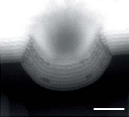
15 Fabricated Ag-Ge multilayer indefinite cavities Cavity size: (L x, L z ) nm (135, 100) nm (170,150) nm (200, 200) nm University of California, Berkeley 18
16 1 Anomalous Scaling in Indefinite Cavities 191 THz 15 k k m 2L i 0 i 0 (170, 150) nm (1, 1, 2) i (1, 1, 1) Transmission (135, 100) nm 140 THz (1, 1, 2) (170, 150) nm (1, 1, 1) (1, 1, 2) THz (200, 200) nm (1, 1, 1) k z /k (200, 200) nm (1, 1, 2) (135, 100 nm) (1, 1, 1) (170, 150) nm (1, 1, 1) (200, 200) nm (1, 1, 1) k 2 x k 2 z 147 THz 191 THz z x 2 2 c Frequency (THz) k x /k 0 University of California, Berkeley 20
17 Q rad, v ~ k 4 Measured Radiation Q (L z = 150 nm) (1, 1, 2) (L z = 200 nm) (1, 1, 2) (L z = 100 nm) (1, 1, 1) 5% Q rad T 1 Q T tot Q rad,v (L z = 150 nm) (1, 1, 1) (L z = 200 nm) (1, 1, 1) T 2 T 1 40 Optical Index n = 17.4! T = T 2 /T (k/k 0 ) 4 The cavity sizes investigated include ( ,100) nm, ( ,150) nm and ( ,200) nm for the (1,1,1) mode, and ( ,150) nm and ( ,200) nm for the (1,1,2) mode. 22
18 Q rad of Indefinite Optical Cavity Cavity radiation Q: Q rad ~ neff Radiation loss from total internal reflection: ~ e ikr e ik r 0 dv k 3 Effective index: n eff k / k 0 Radiation quality factor: Q rad ~ k neff 4 ~ 4 Ref: H.A. Wheeler, Proc IRE, p.1479 (1947); Englund D et al, Opt. Exp.13, 5961 (2005). University of California, Berkeley 24
19 Anomalous Scaling Physics in Indefinite Cavity Cavity size can be scaled well below diffraction limit (/20) Anomalous Scaling: smaller size, higher Q rad ~ k 4 ~ (L) -4 Size-independent resonant frequency High order mode has lower resonance frequency Effective Optical Refractive Index: n =17.4 The total Q, however, is unchanged (metal loss dominated), but Q/V still increases. (Yang et al., Nature Photon. 6, 450, 2012) University of California, Berkeley 25
20 Outline Indefinite Nano Cavity Deep Sub Plasmon Waveguide and Lasers
21 Plasmonics and Its Critical Challenge Surface plasmons dilemma ω Photon ω=ck Surface Plasmon Dispersion Small Mode Size, Short Range ω sp Large Mode Size, Long Range kx Can we have the best of two worlds?


22 Our Approach: Hybride Plasmons Lifting the field out of metal and confined it!


23 Small Mode Size and Relative Long Propagation! Si / SiO 2 / = 1550 nm Mode area ~ 2 /400 L sp ~ 50 microns Oulton, et. al., Nature Photonics (2008) Alam, et., al., CLEO (2007)
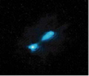
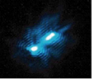
24 Measurement of Deep Sub Mode profile Apertureless NSOM Measured Mode Size (53x65nm) = 633 nm 125nm = nm (Sorger et al. Nature Comm ) Mode Area = 1/50 th of Diffraction Limit Comparable to Transistor or Virus
")
25 Plasmon Laser Realization d = 90 nm h = 5 nm Oulton, et. al, Nature, (2009)

26 Spontaneous Emission to Laser oscillation 0.8 nm i ii iii i ii iii


27 Single mode plasmon Room Temperature 36


28 Multiplexed and Electrically Modulated Plasmon Laser Circuit o Directional emission o Multi colored laser array o Wavelengths multiplexing o Direct electrical modulation Ma, et. al., Nano Lett (2012)

 Emitter (Chang, et al.")
29 Coherent Light Source at Single Molecule Size Single Molecular Bio Sensors Optical Modulators (Sorger, et al., Nanophotonics, 2012) 5 nm Quantum Photonics Signal Control Beam (Gate) Emitter (Chang, et al., PRB, 2010)
30 Possibility of Ultrafast Plasmonic Devices from Broadband Percell Effect Spontaneous emission enhancement (Purcell effect) F n Q V Plasmonics offers: d = 100 nm h = Ultra-small 5 nm modal volume and low Q Broadband Purcell Factor Conventionally, dielectrical cavities (PBG, etc.) pursue High Q due to the diffraction limit High Q > low bandwidth! Ultra Fast Plasmon LED and lasers with Ideally, modulation speed up to 10 THz!
.")
 Broadband (1350-1600 nm) Compact")
31 Graphene Optical Modulator Graphene contains monolayer of carbon atoms, and absorbs the incident light over a broadband (UV to mid-ir). By modulating the Fermi Level of graphene, optical absorption can be turned. Advantages of graphene modulator: Fast (1-100GHz) Broadband ( nm) Compact (25 um 2 ) Athermal (Liu, et. al, Nature, 2011)


 separates")

 I( ) Yin, et.")
32 Photonic Spin Hall Effect in Metamaterials Strong spin orbital interaction ( kˆ kˆ or Ψ) separates light with different helicity Helicity of light: S z I( ) I( ) I( ) I( ) Yin, et., al, Science, (2013)

33 Valley Optoelectronics of 2D WS2 (Spin Valley LED)
34 Acknowledgement Former and Current Members of group: Jun Rho, Renmin Ma, Ong Pholchai, Tongcang Li, Peng Zhang Jie Yao (UC Berkeley) Maiken Mikkelsen (Duke Univ.) Volker Sorger,(George Washington Univ) Rupert Oulton (Imperial College, UK) Xiaobo Yin (Univ. Colorado) Xiaodong Yang (University of Missouri), Yongmin Liu (Northeastern) Peter Park (Samsung), Pavel Kochin (KLA) Collaborators: Prof. Lun Dai of Peking University (CdS nanowire for plasmon laser) Support from: NSF Center for Scalable and Integrated Nao Manufacturing (SINAM) DoD MURIs, DOE
Photonic Micro and Nanoresonators
 Photonic Micro and Nanoresonators Hauptseminar Nanooptics and Nanophotonics IHFG Stuttgart Overview 2 I. Motivation II. Cavity properties and species III. Physics in coupled systems Cavity QED Strong and
Wednesday 3 September Session 3: Metamaterials Theory (16:15 16:45, Huxley LT308)
") Session 3: Metamaterials Theory (16:15 16:45, Huxley LT308) (invited) TBC Session 3: Metamaterials Theory (16:45 17:00, Huxley LT308) Light trapping states in media with longitudinal electric waves D McArthur,
Session 3: Metamaterials Theory (16:15 16:45, Huxley LT308) (invited) TBC Session 3: Metamaterials Theory (16:45 17:00, Huxley LT308) Light trapping states in media with longitudinal electric waves D McArthur,
Quantum Information Processing with Electrons?
 Quantum Information Processing with 10 10 Electrons? René Stock IQIS Seminar, October 2005 People: Barry Sanders Peter Marlin Jeremie Choquette Motivation Quantum information processing realiations Ions
Photonic Crystal Nanocavities for Efficient Light Confinement and Emission
 Journal of the Korean Physical Society, Vol. 42, No., February 2003, pp. 768 773 Photonic Crystal Nanocavities for Efficient Light Confinement and Emission Axel Scherer, T. Yoshie, M. Lončar, J. Vučković
Enhancing the Rate of Spontaneous Emission in Active Core-Shell Nanowire Resonators
 Chapter 6 Enhancing the Rate of Spontaneous Emission in Active Core-Shell Nanowire Resonators 6.1 Introduction Researchers have devoted considerable effort to enhancing light emission from semiconductors
Defect-based Photonic Crystal Cavity for Silicon Laser
 Defect-based Photonic Crystal Cavity for Silicon Laser Final Term Paper for Nonlinear Optics PHYC/ECE 568 Arezou Khoshakhlagh Instructor: Prof. M. Sheikh-Bahae University of New Mexico karezou@unm.edu
Simulations of nanophotonic waveguides and devices using COMSOL Multiphysics
 Presented at the COMSOL Conference 2010 China Simulations of nanophotonic waveguides and devices using COMSOL Multiphysics Zheng Zheng Beihang University 37 Xueyuan Road, Beijing 100191, China Acknowledgement
PLASMONICS/METAMATERIALS
 PLASMONICS/METAMATERIALS Interconnects Optical processing of data Subwavelength confinement Electrodes are in place Coupling to other on-chip devices Combination of guiding, detection, modulation, sensing
Nanomaterials and their Optical Applications
 Nanomaterials and their Optical Applications Winter Semester 2012 Lecture 08 rachel.grange@uni-jena.de http://www.iap.uni-jena.de/multiphoton Outline: Photonic crystals 2 1. Photonic crystals vs electronic
Surface plasmon waveguides
 Surface plasmon waveguides Introduction Size Mismatch between Scaled CMOS Electronics and Planar Photonics Photonic integrated system with subwavelength scale components CMOS transistor: Medium-sized molecule
A Dielectric Invisibility Carpet
 A Dielectric Invisibility Carpet Jensen Li Prof. Xiang Zhang s Research Group Nanoscale Science and Engineering Center (NSEC) University of California at Berkeley, USA CLK08-09/22/2008 Presented at Center
Chapter 5. Photonic Crystals, Plasmonics, and Metamaterials
 Chapter 5. Photonic Crystals, Plasmonics, and Metamaterials Reading: Saleh and Teich Chapter 7 Novotny and Hecht Chapter 11 and 12 1. Photonic Crystals Periodic photonic structures 1D 2D 3D Period a ~
Sub-wavelength electromagnetic structures
 Sub-wavelength electromagnetic structures Shanhui Fan, Z. Ruan, L. Verselegers, P. Catrysse, Z. Yu, J. Shin, J. T. Shen, G. Veronis Ginzton Laboratory, Stanford University http://www.stanford.edu/group/fan
New Aspects of Old Equations: Metamaterials and Beyond (Part 2) 신종화 KAIST 물리학과
 신종화 KAIST 물리학과") New Aspects of Old Equations: Metamaterials and Beyond (Part 2) 신종화 KAIST 물리학과 Metamaterial Near field Configuration in Periodic Structures New Material Material and Metamaterial Material Metamaterial
New Aspects of Old Equations: Metamaterials and Beyond (Part 2) 신종화 KAIST 물리학과 Metamaterial Near field Configuration in Periodic Structures New Material Material and Metamaterial Material Metamaterial
Optical microcavities and nanocavities having both highquality
 Three-dimensional nanometer-scale optical cavities of indefinite medium Jie Yao a, Xiaodong Yang a,b, Xiaobo Yin a,b, Guy Bartal a, and Xiang Zhang a,b,1 a National Science Foundation Nanoscale Science
From Metamaterials to Metadevices
 From Metamaterials to Metadevices Nikolay I. Zheludev Optoelectronics Research Centre & Centre for Photonic Metamaterials University of Southampton, UK www.nanophotonics.org.uk 13 September 2012, Southampton
Left-handed materials: Transfer matrix method studies
 Left-handed materials: Transfer matrix method studies Peter Markos and C. M. Soukoulis Outline of Talk What are Metamaterials? An Example: Left-handed Materials Results of the transfer matrix method Negative
Nanomaterials and their Optical Applications
 Nanomaterials and their Optical Applications Winter Semester 2013 Lecture 02 rachel.grange@uni-jena.de http://www.iap.uni-jena.de/multiphoton Lecture 2: outline 2 Introduction to Nanophotonics Theoretical
Laser Basics. What happens when light (or photon) interact with a matter? Assume photon energy is compatible with energy transition levels.
 interact with a matter? Assume photon energy is compatible with energy transition levels.") What happens when light (or photon) interact with a matter? Assume photon energy is compatible with energy transition levels. Electron energy levels in an hydrogen atom n=5 n=4 - + n=3 n=2 13.6 = [ev]
What happens when light (or photon) interact with a matter? Assume photon energy is compatible with energy transition levels. Electron energy levels in an hydrogen atom n=5 n=4 - + n=3 n=2 13.6 = [ev]
Negative epsilon medium based optical fiber for transmission around UV and visible region
 I J C T A, 9(8), 2016, pp. 3581-3587 International Science Press Negative epsilon medium based optical fiber for transmission around UV and visible region R. Yamuna Devi*, D. Shanmuga Sundar** and A. Sivanantha
The Broadband Fixed-Angle Source Technique (BFAST) LUMERICAL SOLUTIONS INC
 LUMERICAL SOLUTIONS INC") The Broadband Fixed-Angle Source Technique (BFAST) LUMERICAL SOLUTIONS INC. 1 Outline Introduction Lumerical s simulation products Simulation of periodic structures The new Broadband Fixed-Angle Source
The Broadband Fixed-Angle Source Technique (BFAST) LUMERICAL SOLUTIONS INC. 1 Outline Introduction Lumerical s simulation products Simulation of periodic structures The new Broadband Fixed-Angle Source
Electromagnetic Metamaterials
 Photonic Bandgap and Electromagnetic Metamaterials Andrew Kirk andrew.kirk@mcgill.ca ca Department of Electrical and Computer Engineering McGill Institute for Advanced Materials A Kirk 11/24/2008 Photonic
Nanoscale optical circuits: controlling light using localized surface plasmon resonances
 Nanoscale optical circuits: controlling light using localized surface plasmon resonances T. J. Davis, D. E. Gómez and K. C. Vernon CSIRO Materials Science and Engineering Localized surface plasmon (LSP)
Air-holes radius change effects and structure transitions in the linear photonic crystal nanocavities
 American Journal of Optics and Photonics 2013; 1(3): 11-16 Published online June 20, 2013 (http://www.sciencepublishinggroup.com/j/ajop) doi: 10.11648/j.ajop.20130103.11 Air-holes radius change effects
SUPPLEMENTARY INFORMATION
 SUPPLEMENTARY INFORMATION doi: 10.1038/nPHYS1804 Supplementary Information J. Zhu 1, J. Christensen 2, J. Jung 2,3, L. Martin-Moreno 4, X. Yin 1, L. Fok 1, X. Zhang 1 and F. J. Garcia-Vidal 2 1 NSF Nano-scale
Investigation on Mode Splitting and Degeneracy in the L3 Photonic Crystal Nanocavity via Unsymmetrical Displacement of Air-Holes
 The International Journal Of Engineering And Science (Ijes) Volume 2 Issue 2 Pages 146-150 2013 Issn: 2319 1813 Isbn: 2319 1805 Investigation on Mode Splitting and Degeneracy in the L3 Photonic Crystal
Photonic devices for quantum information processing:
 Outline Photonic devices for quantum information processing: coupling to dots, structure design and fabrication Optoelectronics Group, Cavendish Lab Outline Vuckovic s group Noda s group Outline Outline
From optical graphene to topological insulator
 From optical graphene to topological insulator Xiangdong Zhang Beijing Institute of Technology (BIT), China zhangxd@bit.edu.cn Collaborator: Wei Zhong (PhD student, BNU) Outline Background: From solid
Optical nonlocality induced Zitterbewegung near the Dirac point in metal-dielectric multilayer metamaterials
 Optical nonlocality induced Zitterbewegung near the Dirac point in metal-dielectric multilayer metamaterials Lei Sun, 1 Jie Gao, 2 and Xiaodong Yang 3 1 Department of Mechanical and Aerospace Engineering,
Analysis of Photonic Band Structure in 1-D Photonic Crystal using PWE and FDTD Method
 P P IJISET - International Journal of Innovative Science, Engineering & Technology, Vol. Issue 8, August 05. Analysis of Photonic Band Structure in -D Photonic Crystal using PWE and FDTD Method Pooja ChhokerP
Monolayer Semiconductors
 Monolayer Semiconductors Gilbert Arias California State University San Bernardino University of Washington INT REU, 2013 Advisor: Xiaodong Xu (Dated: August 24, 2013) Abstract Silicon may be unable to
Alexander Gaeta Department of Applied Physics and Applied Mathematics Michal Lipson Department of Electrical Engineering
 Chip-Based Optical Frequency Combs Alexander Gaeta Department of Applied Physics and Applied Mathematics Michal Lipson Department of Electrical Engineering KISS Frequency Comb Workshop Cal Tech, Nov. 2-5,
A COMPACT POLARIZATION BEAM SPLITTER BASED ON A MULTIMODE PHOTONIC CRYSTAL WAVEGUIDE WITH AN INTERNAL PHOTONIC CRYSTAL SECTION
 Progress In Electromagnetics Research, PIER 103, 393 401, 2010 A COMPACT POLARIZATION BEAM SPLITTER BASED ON A MULTIMODE PHOTONIC CRYSTAL WAVEGUIDE WITH AN INTERNAL PHOTONIC CRYSTAL SECTION Y. C. Shi Centre
Lei Zhou Physics Department, Fudan University, Shanghai , China
 Tunable Meta-surfaces for Active Manipulations of Electromagnetic Waves Lei Zhou Physics Department, Fudan University, Shanghai 200433, China phzhou@fudan.edu.cn Acknowledgements Key collaborators Yuanbo
Efficient light emission from LEDs, OLEDs, and nanolasers via surface-plasmon resonance
 Efficient light emission from LEDs, OLEDs, and nanolasers via surface-plasmon resonance Seok Ho Song, Hanyang University, http://optics.anyang.ac.kr/~shsong silver grating Key notes 1. How does the surface
Computational Electromagnetics: from Metamaterials to Particle Accelerators
 Computational Electromagnetics: from Metamaterials to Particle Accelerators Arya Fallahi Ultrafast optics and X-ray Division 1. July 213 2/44 Outline Ø Frequency Selective Surfaces (FSS) Analysis techniques:
Superconductivity Induced Transparency
 Superconductivity Induced Transparency Coskun Kocabas In this paper I will discuss the effect of the superconducting phase transition on the optical properties of the superconductors. Firstly I will give
Radiation-matter interaction.
 Radiation-matter interaction Radiation-matter interaction Classical dipoles Dipole radiation Power radiated by a classical dipole in an inhomogeneous environment The local density of optical states (LDOS)
Highly Efficient Graphene-Based Optical Modulator With Edge Plasmonic Effect
 Highly Efficient Graphene-Based Optical Modulator With Edge Plasmonic Effect Ran Hao, Ziwei Ye, Xiliang Peng, Yijie Gu, JianYao Jiao, Haixia Zhu, Wei E. I. Sha, and Erping Li Key Laboratory of Advanced
Symmetry Breaking and Optical Negative Index of Closed Nanorings
 Supplementary Information Symmetry Breaking and Optical Negative Index of Closed Nanorings Boubacar Kanté 1, Yong-Shik Park 1, Kevin O Brien 1, Daniel Shuldman 1, Norberto D. Lanzillotti Kimura 1, Zi Jing
SCATTERING OF ELECTROMAGNETIC WAVES ON METAL NANOPARTICLES. Tomáš Váry, Juraj Chlpík, Peter Markoš
 SCATTERING OF ELECTROMAGNETIC WAVES ON METAL NANOPARTICLES Tomáš Váry, Juraj Chlpík, Peter Markoš ÚJFI, FEI STU, Bratislava E-mail: tomas.vary@stuba.sk Received xx April 2012; accepted xx May 2012. 1.
ECE 484 Semiconductor Lasers
 ECE 484 Semiconductor Lasers Dr. Lukas Chrostowski Department of Electrical and Computer Engineering University of British Columbia January, 2013 Module Learning Objectives: Understand the importance of
Quantum optics and optomechanics
 Quantum optics and optomechanics 740nm optomechanical crystals LIGO mirror AMO: Alligator nanophotonic waveguide quantum electro-mechanics Oskar Painter, Jeff Kimble, Keith Schwab, Rana Adhikari, Yanbei
Time Domain Modeling of All-Optical Switch based on PT-Symmetric Bragg Grating
 Time Domain Modeling of All-Optical Switch based on PT-Symmetric Bragg Grating Sendy Phang 1, Ana Vukovic 1, Hadi Susanto 2, Trevor M. Benson 1, and Phillip Sewell 1 1 School of Electrical and Electronic
Understanding Nanoplasmonics. Greg Sun University of Massachusetts Boston
 Understanding Nanoplasmonics Greg Sun University of Massachusetts Boston Nanoplasmonics Space 100pm 1nm 10nm 100nm 1μm 10μm 100μm 1ns 100ps 10ps Photonics 1ps 100fs 10fs 1fs Time Surface Plasmons Surface
Workshop on New Materials for Renewable Energy
 2286-6 Workshop on New Materials for Renewable Energy 31 October - 11 November 201 Metamaterials: Past, Present, and Future Nonlinear Physics Centre Research School of Physics and Engineering The Australian
ECE280: Nano-Plasmonics and Its Applications. Week8. Negative Refraction & Plasmonic Metamaterials
 ECE8: Nano-Plasonics and Its Applications Week8 Negative Refraction & Plasonic Metaaterials Anisotropic Media c k k y y ω μ μ + Dispersion relation for TM wave isotropic anisotropic k r k i, S i S r θ
Optimizing the performance of metal-semiconductor-metal photodetectors by embedding nanoparticles in the absorption layer
 Journal of Electrical and Electronic Engineering 2015; 3(2-1): 78-82 Published online February 10, 2015 (http://www.sciencepublishinggroup.com/j/jeee) doi: 10.11648/j.jeee.s.2015030201.27 ISSN: 2329-1613
Introduction to Photonic Crystals
 1 Introduction to Photonic Crystals Summary. Chapter 1 gives a brief introduction into the basics of photonic crystals which are a special class of optical media with periodic modulation of permittivity.
Design of a Multi-Mode Interference Crossing Structure for Three Periodic Dielectric Waveguides
 Progress In Electromagnetics Research Letters, Vol. 75, 47 52, 2018 Design of a Multi-Mode Interference Crossing Structure for Three Periodic Dielectric Waveguides Haibin Chen 1, Zhongjiao He 2,andWeiWang
Seminars in Nanosystems - I
 Seminars in Nanosystems - I Winter Semester 2011/2012 Dr. Emanuela Margapoti Emanuela.Margapoti@wsi.tum.de Dr. Gregor Koblmüller Gregor.Koblmueller@wsi.tum.de Seminar Room at ZNN 1 floor Topics of the
Introduction to Nonlinear Optics
 Introduction to Nonlinear Optics Prof. Cleber R. Mendonca http://www.fotonica.ifsc.usp.br Outline Linear optics Introduction to nonlinear optics Second order nonlinearities Third order nonlinearities Two-photon
Nanophysics: Main trends
 Nano-opto-electronics Nanophysics: Main trends Nanomechanics Main issues Light interaction with small structures Molecules Nanoparticles (semiconductor and metallic) Microparticles Photonic crystals Nanoplasmonics
Nonlinear Electrodynamics and Optics of Graphene
 Nonlinear Electrodynamics and Optics of Graphene S. A. Mikhailov and N. A. Savostianova University of Augsburg, Institute of Physics, Universitätsstr. 1, 86159 Augsburg, Germany E-mail: sergey.mikhailov@physik.uni-augsburg.de
Chemistry Instrumental Analysis Lecture 5. Chem 4631
 Chemistry 4631 Instrumental Analysis Lecture 5 Light Amplification by Stimulated Emission of Radiation High Intensities Narrow Bandwidths Coherent Outputs Applications CD/DVD Readers Fiber Optics Spectroscopy
Beyond Stefan-Boltzmann Law: Thermal Hyper- Conductivity
 Purdue University Purdue e-pubs Birck and NCN Publications Birck Nanotechnology Center 5-6-2012 Beyond Stefan-Boltzmann Law: Thermal Hyper- Conductivity Evgenii E. Narimanov Birck Nanotechnology Center,
Title. Author(s)Nagasaki, Akira; Saitoh, Kunimasa; Koshiba, Masanori. CitationOptics Express, 19(4): Issue Date Doc URL.
Nagasaki, Akira; Saitoh, Kunimasa; Koshiba, Masanori. CitationOptics Express, 19(4): Issue Date Doc URL.") Title Polarization characteristics of photonic crystal fib Author(s)Nagasaki, Akira; Saitoh, Kunimasa; Koshiba, Masanori CitationOptics Express, 19(4): 3799-3808 Issue Date 2011-02-14 Doc URL http://hdl.handle.net/2115/45257
Title Polarization characteristics of photonic crystal fib Author(s)Nagasaki, Akira; Saitoh, Kunimasa; Koshiba, Masanori CitationOptics Express, 19(4): 3799-3808 Issue Date 2011-02-14 Doc URL http://hdl.handle.net/2115/45257
Towards optical left-handed metamaterials
 FORTH Tomorrow: Modelling approaches for metamaterials Towards optical left-handed metamaterials M. Kafesaki, R. Penciu, Th. Koschny, P. Tassin, E. N. Economou and C. M. Soukoulis Foundation for Research
Tooth-shaped plasmonic waveguide filters with nanometeric. sizes
 Tooth-shaped plasmonic waveguide filters with nanometeric sizes Xian-Shi LIN and Xu-Guang HUANG * Laboratory of Photonic Information Technology, South China Normal University, Guangzhou, 510006, China
transmission reflection absorption
 Optical Cages V. Kumar*, J. P. Walker* and H. Grebel The Electronic Imaging Center and the ECE department at NJIT, Newark, NJ 0702. grebel@njit.edu * Contributed equally Faraday Cage [], a hollow structure
Lecture 14 Dispersion engineering part 1 - Introduction. EECS Winter 2006 Nanophotonics and Nano-scale Fabrication P.C.Ku
 Lecture 14 Dispersion engineering part 1 - Introduction EEC 598-2 Winter 26 Nanophotonics and Nano-scale Fabrication P.C.Ku chedule for the rest of the semester Introduction to light-matter interaction
Dr. Tao Li
 Tao Li taoli@nju.edu.cn Nat. Lab. of Solid State Microstructures Department of Materials Science and Engineering Nanjing University Concepts Basic principles Surface Plasmon Metamaterial Summary Light
Strong coupling between mid-infrared localized plasmons and phonons
 Strong coupling between mid-infrared localized plasmons and phonons Weiwei Wan, 1 Xiaodong Yang, 1,2 and Jie Gao 1,* 1 Department of Mechanical and Aerospace Engineering, Missouri University of Science
Single Semiconductor Nanostructures for Quantum Photonics Applications: A solid-state cavity-qed system with semiconductor quantum dots
 The 3 rd GCOE Symposium 2/17-19, 19, 2011 Tohoku University, Sendai, Japan Single Semiconductor Nanostructures for Quantum Photonics Applications: A solid-state cavity-qed system with semiconductor quantum
Lecture 3: Optical Properties of Insulators, Semiconductors, and Metals. 5 nm
 Metals Lecture 3: Optical Properties of Insulators, Semiconductors, and Metals 5 nm Course Info Next Week (Sept. 5 and 7) no classes First H/W is due Sept. 1 The Previous Lecture Origin frequency dependence
Strong Coupling between On Chip Notched Ring Resonator and Nanoparticle
 Strong Coupling between On Chip Notched Ring Resonator and Nanoparticle S. Wang 1, K. Broderick 1, 3, H. Smith 1 2, 3,1 *, and Y. Yi 1 Massauchusetts Institute of Technology, Cambridge, MA 02139 2 New
Supporting Information
 Supporting Information Light emission near a gradient metasurface Leonard C. Kogos and Roberto Paiella Department of Electrical and Computer Engineering and Photonics Center, Boston University, Boston,
Zeroth-order transmission resonance in hyperbolic metamaterials
 Purdue University Purdue e-pubs Birck and NCN Publications Birck Nanotechnology Center 6-17-2013 Zeroth-order transmission resonance in hyperbolic metamaterials Zun Huang Birck Nanotechnology Center, Purdue
Energy transport in metal nanoparticle plasmon waveguides
 Energy transport in metal nanoparticle plasmon waveguides Stefan A. Maier, Pieter G. Kik, and Harry A. Atwater California Institute of Technology Thomas J. Watson Laboratory of Applied Physics, Pasadena,
Plasmonic nanoguides and circuits
 Plasmonic nanoguides and circuits Introduction: need for plasmonics? Strip SPPs Cylindrical SPPs Gap SPP waveguides Channel plasmon polaritons Dielectric-loaded SPP waveguides PLASMOCOM 1. Intro: need
EPSILON-NEAR-ZERO (ENZ) AND MU-NEAR-ZERO (MNZ) MATERIALS
 AND MU-NEAR-ZERO (MNZ) MATERIALS") EPSILON-NEAR-ZERO (ENZ) AND MU-NEAR-ZERO (MNZ) MATERIALS SARAH NAHAR CHOWDHURY PURDUE UNIVERSITY 1 Basics Design ENZ Materials Lumped circuit elements Basics Decoupling Direction emission Tunneling Basics
EPSILON-NEAR-ZERO (ENZ) AND MU-NEAR-ZERO (MNZ) MATERIALS SARAH NAHAR CHOWDHURY PURDUE UNIVERSITY 1 Basics Design ENZ Materials Lumped circuit elements Basics Decoupling Direction emission Tunneling Basics
Cavity QED: Quantum Control with Single Atoms and Single Photons. Scott Parkins 17 April 2008
 Cavity QED: Quantum Control with Single Atoms and Single Photons Scott Parkins 17 April 2008 Outline Quantum networks Cavity QED - Strong coupling cavity QED - Network operations enabled by cavity QED
Room-temperature continuous-wave lasing from monolayer molybdenum ditelluride integrated with a silicon nanobeam cavity
 In the format provided by the authors and unedited. DOI: 10.1038/NNANO.2017.128 Room-temperature continuous-wave lasing from monolayer molybdenum ditelluride integrated with a silicon nanobeam cavity Yongzhuo
arxiv: v1 [physics.optics] 1 May 2011
![arxiv: v1 [physics.optics] 1 May 2011](/thumbs/74/70729533.jpg "arxiv: v1 [physics.optics] 1 May 2011") Robust method to determine the resolution of a superlens by analyzing the near-field image of a two-slit object B. D. F. Casse, W. T. Lu, Y. J. Huang, and S. Sridhar Electronic Materials Research Institute
Robust method to determine the resolution of a superlens by analyzing the near-field image of a two-slit object B. D. F. Casse, W. T. Lu, Y. J. Huang, and S. Sridhar Electronic Materials Research Institute
Acoustic metamaterials in nanoscale
 Acoustic metamaterials in nanoscale Dr. Ari Salmi www.helsinki.fi/yliopisto 12.2.2014 1 Revisit to resonances Matemaattis-luonnontieteellinen tiedekunta / Henkilön nimi / Esityksen nimi www.helsinki.fi/yliopisto
Micro- and Nano-Technology... for Optics
 Micro- and Nano-Technology...... for Optics U.D. Zeitner Fraunhofer Institut für Angewandte Optik und Feinmechanik Jena Today: 1. Introduction E. Bernhard Kley Institute of Applied Physics Friedrich-Schiller
Lecture 0. NC State University
 Chemistry 736 Lecture 0 Overview NC State University Overview of Spectroscopy Electronic states and energies Transitions between states Absorption and emission Electronic spectroscopy Instrumentation Concepts
Strong Absorption in a 2D Materials-based Spiral Nanocavity
 1858 PIERS Proceedings, Prague, Czech Republic, July 6 9, 2015 Strong Absorption in a 2D Materials-based Spiral Nanocavity Mohammad H. Tahersima and Volker J. Sorger Department of Electrical and Computer
Quantum Optics in Wavelength Scale Structures
 Quantum Optics in Wavelength Scale Structures SFB Summer School Blaubeuren July 2012 J. G. Rarity University of Bristol john.rarity@bristol.ac.uk Confining light: periodic dielectric structures Photonic
History of photonic crystals and metamaterials. However, many serious obstacles must be overcome before the impressive possibilities
 TECHNICAL NOTEBOOK I back to basics BACK TO BASICS: History of photonic crystals and metamaterials Costas M. SOUKOULIS 1,2 1 Ames Laboratory and Department of Physics, Iowa State University, Ames, Iowa,
Research Article Si Substrate-Based Metamaterials for Ultrabroadband Perfect Absorption in Visible Regime
 Nanomaterials, Article ID 893202, 5 pages http://dx.doi.org/0.55/204/893202 Research Article Si Substrate-Based Metamaterials for Ultrabroadband Perfect in Visible Regime Qi Han, Lei Jin, Yongqi Fu, and
Photonic crystal laser threshold analysis using 3D FDTD with a material gain model
 Photonic crystal laser threshold analysis using 3D FDTD with a material gain model Adam Mock and John O'Brien Microphotonic Device Group University of Southern California July 14, 2009 Session: ITuD6 Integrated
Light Manipulation by Metamaterials
 Light Manipulation by Metamaterials W. J. Sun, S. Y. Xiao, Q. He*, L. Zhou Physics Department, Fudan University, Shanghai 200433, China *Speaker: qionghe@fudan.edu.cn 2011/2/19 Outline Background of metamaterials
Tuning the far-field superlens: from UV to visible
 Tuning the far-field superlens: from UV to visible Yi Xiong, Zhaowei Liu, Stéphane Durant, Hyesog Lee, Cheng Sun, and Xiang Zhang* 510 Etcheverry Hall, NSF Nanoscale Science and Engineering Center (NSEC),
Demonstration of Near-Infrared Negative-Index Materials
 Demonstration of Near-Infrared Negative-Index Materials Shuang Zhang 1, Wenjun Fan 1, N. C. Panoiu 2, K. J. Malloy 1, R. M. Osgood 2 and S. R. J. Brueck 2 1. Center for High Technology Materials and Department
Spring 2009 EE 710: Nanoscience and Engineering
 Spring 009 EE 710: Nanoscience and Engineering Part 10: Surface Plasmons in Metals Images and figures supplied from Hornyak, Dutta, Tibbals, and Rao, Introduction to Nanoscience, CRC Press Boca Raton,
1. Reminder: E-Dynamics in homogenous media and at interfaces
 0. Introduction 1. Reminder: E-Dynamics in homogenous media and at interfaces 2. Photonic Crystals 2.1 Introduction 2.2 1D Photonic Crystals 2.3 2D and 3D Photonic Crystals 2.4 Numerical Methods 2.5 Fabrication
Refractive Index Measurement by Gain- or Loss-Induced Resonance
 Refractive Index Measurement by Gain- or Loss-Induced Resonance 59 Refractive Index Measurement by Gain- or Loss-Induced Resonance Markus Miller Using a semiconductor optical resonator consisting of a
Supplementary Figure 1: A potential scheme to electrically gate the graphene-based metamaterial. Here density. The voltage equals, where is the DC
 Supplementary Figure 1: A potential scheme to electrically gate the graphene-based metamaterial. Here density. The voltage equals, where is the DC permittivity of the dielectric. is the surface charge
Rezonanse typu spin-orbit w meta-materiałowych elementach nanofotoniki Spin-orbit resonances in meta-material elements of nanophotonics
 Rezonanse typu spin-orbit w meta-materiałowych elementach nanofotoniki Spin-orbit resonances in meta-material elements of nanophotonics Wojciech Nasalski Zespół Badawczy Nanofotoniki Instytut Podstawowych
A Novel Design of Photonic Crystal Lens Based on Negative Refractive Index
 PIERS ONLINE, VOL. 4, NO. 2, 2008 296 A Novel Design of Photonic Crystal Lens Based on Negative Refractive Index S. Haxha 1 and F. AbdelMalek 2 1 Photonics Group, Department of Electronics, University
Gradient-index metamaterials and spoof surface plasmonic waveguide
 Gradient-index metamaterials and spoof surface plasmonic waveguide Hui Feng Ma State Key Laboratory of Millimeter Waves Southeast University, Nanjing 210096, China City University of Hong Kong, 11 October
Ge Quantum Well Modulators on Si. D. A. B. Miller, R. K. Schaevitz, J. E. Roth, Shen Ren, and Onur Fidaner
 10.1149/1.2986844 The Electrochemical Society Ge Quantum Well Modulators on Si D. A. B. Miller, R. K. Schaevitz, J. E. Roth, Shen Ren, and Onur Fidaner Ginzton Laboratory, 450 Via Palou, Stanford CA 94305-4088,
PANDA ring resonator for optical Gas and Pressure sensing applications
 I J C T A, 9(8), 016, pp. 3415-34 International Science Press PANDA ring resonator for optical Gas and Pressure sensing applications G. Bhuvaneswari*, D. Shanmuga sundar* and A. Sivanantha Raja* ABSTRACT
Directional emitter and beam splitter based on self-collimation effect
 Directional emitter and beam splitter based on self-collimation effect W. Y. Liang, J. W. Dong, and H. Z. Wang* State Key Laboratory of Optoelectronic Materials and Technologies, Zhongshan (Sun Yat-Sen)
FIBER OPTICS. Prof. R.K. Shevgaonkar. Department of Electrical Engineering. Indian Institute of Technology, Bombay. Lecture: 17.
 FIBER OPTICS Prof. R.K. Shevgaonkar Department of Electrical Engineering Indian Institute of Technology, Bombay Lecture: 17 Optical Sources- Introduction to LASER Fiber Optics, Prof. R.K. Shevgaonkar,
Supporting information. Unidirectional Doubly Enhanced MoS 2 Emission via
 Supporting information Unidirectional Doubly Enhanced MoS 2 Emission via Photonic Fano Resonances Xingwang Zhang, Shinhyuk Choi, Dake Wang, Carl H. Naylor, A. T. Charlie Johnson, and Ertugrul Cubukcu,,*
FINITE-DIFFERENCE FREQUENCY-DOMAIN ANALYSIS OF NOVEL PHOTONIC
 FINITE-DIFFERENCE FREQUENCY-DOMAIN ANALYSIS OF NOVEL PHOTONIC WAVEGUIDES Chin-ping Yu (1) and Hung-chun Chang (2) (1) Graduate Institute of Electro-Optical Engineering, National Taiwan University, Taipei,
Ultra-Slow Light Propagation in Room Temperature Solids. Robert W. Boyd
 Ultra-Slow Light Propagation in Room Temperature Solids Robert W. Boyd The Institute of Optics and Department of Physics and Astronomy University of Rochester, Rochester, NY USA http://www.optics.rochester.edu
SUPPLEMENTARY INFORMATION
 On-chip zero-index metamaterials Yang Li 1, Shota Kita 1, Philip Muñoz 1, Orad Reshef 1, Daryl I. Vulis 1, Mei Yin 1,, Marko Lončar 1 *, and Eric Mazur 1,3 * Supplementary Information: Materials and Methods