Other SPM Techniques. Scanning Probe Microscopy HT10
|
|
|
- Gabriella Cori Wilcox
- 5 years ago
- Views:
Transcription
1 Other SPM Techniques Scanning Near-Field Optical Microscopy (SNOM) Scanning Capacitance Microscopy (SCM) Scanning Spreading Resistance Microscopy (SSRM) Multiprobe techniques Electrostatic Force Microscopy, Kelvin probe force microscopy 1
2 2
3 Scanning Near-Field Optical Microscopy (SNOM) Optical microscope resolution limit: 0.61λ (Abbè limit) Optical properties of nanostructures very important.. Light-emitting nanoparticles, molecules, devices.. Inelastic scattering: Raman, fluorescence SNOM uses the optical near-field, non-radiative local electric field, evanescent at surfaces Near-field interactions lead to far-field changes Detector close to the surface, resolution in the nm range Problem: tip preparation (standard SNOM) 3
4 SNOM basics Dipole-dipole interaction (near field) lead to far-field changes Overview of SNOM modes: a) Aperture SNOM b) scattering (aperture-less) SNOM c)-d): Related STM techniques 4


5 Aperture SNOM Optical fiber tips - tapered - metal coated - end aperture Many configurations for aperture SNOM Distance control crucial - tip shear forces (NT-MDT design) 5

 Single dye")


6 Aperture SNOM example Illumination collection mode Hosaka and Saiki, J. Microsc.202, 362 (2001) Single dye molecules - fluorescence - 15 nm res. Aperture: 20 nm Resolution 15 nm better than fundamental limit in standard SNOM on metal surfaces (30-50 nm) 6
7 Scattering SNOM Relies on field enhancement due to metallic tip - surface plasmons Raman scattering - SERS effect enhances signal up to Raman spectroscopy -very useful for nanostructures, molecules, CNT Measures vibrational modes - fingerprint for different bonds and molecules example: radial breathing mode in CNT - Raman shift direct measure of diameter (figure: diameters nm) CNT far-field Raman spectrum (a) near-field, (b) far-field, (c) difference 7

 and TERS Raman")
 and SFM")
8 TERS - Tip-enhanced Raman spectroscopy Images of a CNT bundle by standard confocal Raman (left) and TERS Raman (right) Branching CNT viewed by TERS Raman (left) and SFM (right) 8

9 Instrumentation for TERS SFM Micro-Raman spectrometer including: confocal microscope focused laser monochromator detectors Example NT-MDT Ntegra Spectra 9
10 Scanning Capacitance Microscopy SCM useful for measuring dopant profiles on the nanoscale Model: MOS structure 1 C tot = 1 C air + 1 C ox + 1 C D 10
11 SCM 1 = C tot C air C ox C D (Note: sample bias!) 11
12 SCM instrumentation Contact-mode SFM AC bias, measure dc/dv Special capacitance sensor 12


13 SCM examples SCM of 0.6 µm n-channel MOSFET From Edwards, APL 72, 698 SFM and SCM images of an SRAM device 13
14 Scanning Spreading Resistance Microscopy (SSRM) Measure spreading resistance by pressing the SFM tip into the sample - large force due to contamination Maxwell formula: R = " 4a Nanoscale contact: ballistic transport => Sharvin formula: h 2 " F R Sharvin = 2e 2 Equal or better resolution than SCM # 2 a 2 more simple determination of doping level, but cannot determine carrier type surface damage due to indentation 14

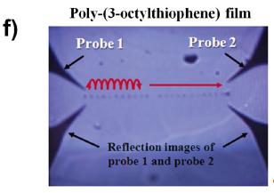
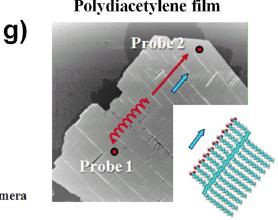
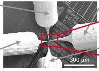
15 Multiprobe techniques Local conductivity measurements on nanostructures, nanoelectronic devices, organic layers, etc. Example: Single-electron transistor (SET) 15
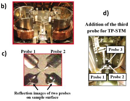
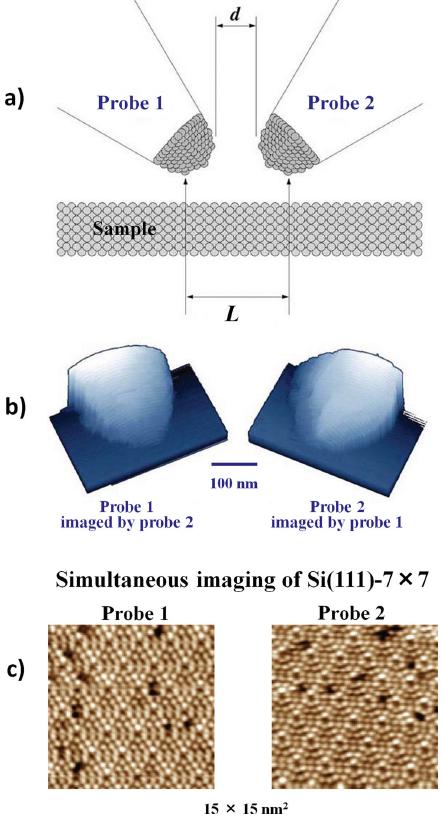
16 Double-probe STM 16
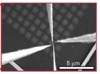
 and d), respectively. An atomic-resolution STM image of a Si (111)7x7 surface obtained by using this WO x nanorod probe is shown in e).")
17 Sharper tips Figure 5. Schematic diagram of minimum interprobe distance, L min, between two probes; a) two conventional W probes, b) two WO x nanorod probes grown at apexes of two W probes. SEM and TEM images of the WO x nanorods are shown in c) and d), respectively. An atomic-resolution STM image of a Si (111)7x7 surface obtained by using this WO x nanorod probe is shown in e). 17
18 Resistance measurements 18
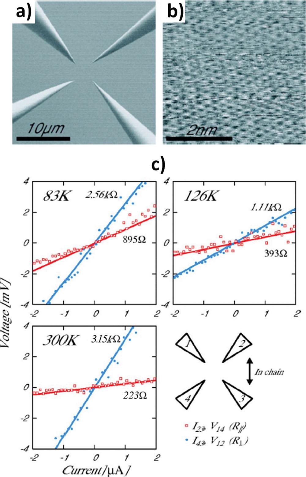
19 Quadrupleprobe HOPG V-I measurements on Si(111)4x1-In, a 1-dim. surface structure 19

20 Electrostatic Force Microscopy Special case of DFM Synonymous: Kelvin probe force microscopy 20
21 EFM, Kelvin probe measurements Add AC signal to DC bias F el = "C ( "z V bias # V CPD +V AC cos$ m t ) 2 F el = "C "z [( V bias # V CPD ) V AC cos$ m t( V bias # V CPD ) +V AC cos 2 $m t] Force contains DC, ω m and 2ω m components ω m component zero when V bias = V CPD ω m component zero detected by lock-in technique 21
Agilent Technologies. Scanning Microwave Microscopy (SMM)
") Agilent Technologies Scanning Microwave Microscopy (SMM) Expanding Impedance Measurements to the Nanoscale: Coupling the Power of Scanning Probe Microscopy with the PNA Presented by: Craig Wall PhD Product
Agilent Technologies Scanning Microwave Microscopy (SMM) Expanding Impedance Measurements to the Nanoscale: Coupling the Power of Scanning Probe Microscopy with the PNA Presented by: Craig Wall PhD Product
Optics and Spectroscopy
 Introduction to Optics and Spectroscopy beyond the diffraction limit Chi Chen 陳祺 Research Center for Applied Science, Academia Sinica 2015Apr09 1 Light and Optics 2 Light as Wave Application 3 Electromagnetic
Fundamentals of nanoscience
 Fundamentals of nanoscience Spectroscopy of nano-objects Mika Pettersson 1. Non-spatially resolved spectroscopy Traditionally, in spectroscopy, one is interested in obtaining information on the energy
Magnetic Force Microscopy (MFM) F = µ o (m )H
 F = µ o (m )H") Magnetic Force Microscopy (MFM) F = µ o (m )H 1. MFM is based on the use of a ferromagnetic tip as a local field sensor. Magnetic interaction between the tip and the surface results in a force acting on
Magnetic Force Microscopy (MFM) F = µ o (m )H 1. MFM is based on the use of a ferromagnetic tip as a local field sensor. Magnetic interaction between the tip and the surface results in a force acting on
SCANNING-PROBE TECHNIQUES OR APPARATUS; APPLICATIONS OF SCANNING-PROBE TECHNIQUES, e.g. SCANNING PROBE MICROSCOPY [SPM]
![SCANNING-PROBE TECHNIQUES OR APPARATUS; APPLICATIONS OF SCANNING-PROBE TECHNIQUES, e.g. SCANNING PROBE MICROSCOPY [SPM]](/thumbs/81/83165631.jpg "SCANNING-PROBE TECHNIQUES OR APPARATUS; APPLICATIONS OF SCANNING-PROBE TECHNIQUES, e.g. SCANNING PROBE MICROSCOPY [SPM]") G01Q SCANNING-PROBE TECHNIQUES OR APPARATUS; APPLICATIONS OF SCANNING-PROBE TECHNIQUES, e.g. SCANNING PROBE MICROSCOPY [SPM] Scanning probes, i.e. devices having at least a tip of nanometre sized dimensions
G01Q SCANNING-PROBE TECHNIQUES OR APPARATUS; APPLICATIONS OF SCANNING-PROBE TECHNIQUES, e.g. SCANNING PROBE MICROSCOPY [SPM] Scanning probes, i.e. devices having at least a tip of nanometre sized dimensions
Scanning Probe Microscopy. Amanda MacMillan, Emmy Gebremichael, & John Shamblin Chem 243: Instrumental Analysis Dr. Robert Corn March 10, 2010
 Scanning Probe Microscopy Amanda MacMillan, Emmy Gebremichael, & John Shamblin Chem 243: Instrumental Analysis Dr. Robert Corn March 10, 2010 Scanning Probe Microscopy High-Resolution Surface Analysis
TEOS characterization of 2D materials from graphene to TMDCs
 Marc Chaigneau Yoshito Okuno, Andrey Krayev, Filippo Fabbri HORIBA Scientific AIST-NT Inc. IMEM-CNR Institute TEOS characterization of 2D materials from graphene to TMDCs 30-03-2017 Graphene2017 2015 2017
Electrical Characterization with SPM Application Modules
 Electrical Characterization with SPM Application Modules Metrology, Characterization, Failure Analysis: Data Storage Magnetoresistive (MR) read-write heads Semiconductor Transistors Interconnect Ferroelectric
Near-Field Nano/Atom Optics and Technology
 M. Ohtsu (Ed.) Near-Field Nano/Atom Optics and Technology With 189 Figures / Springer Preface List of Contributors V VII XIII 1. Introduction 1 1.1 Near-Field Optics and Related Technologies 1 1.2 History
Bringing optics into the nanoscale a double-scanner AFM brings advanced optical experiments within reach
 Bringing optics into the nanoscale a double-scanner AFM brings advanced optical experiments within reach Beyond the diffraction limit The resolution of optical microscopy is generally limited by the diffraction
Scattering-type near-field microscopy for nanoscale optical imaging
 Scattering-type near-field microscopy for nanoscale optical imaging Rainer Hillenbrand Nano-Photonics Group Max-Planck-Institut für Biochemie 82152 Martinsried, Germany Infrared light enables label-free
Università degli Studi di Bari "Aldo Moro"
 Università degli Studi di Bari "Aldo Moro" Table of contents 1. Introduction to Atomic Force Microscopy; 2. Introduction to Raman Spectroscopy; 3. The need for a hybrid technique Raman AFM microscopy;
Introduction to Scanning Probe Microscopy Zhe Fei
 Introduction to Scanning Probe Microscopy Zhe Fei Phys 590B, Apr. 2019 1 Outline Part 1 SPM Overview Part 2 Scanning tunneling microscopy Part 3 Atomic force microscopy Part 4 Electric & Magnetic force
Scanning Probe Microscopy (SPM)
") Scanning Probe Microscopy (SPM) Scanning Tunneling Microscopy (STM) --- G. Binnig, H. Rohrer et al, (1982) Near-Field Scanning Optical Microscopy (NSOM) --- D. W. Pohl (1982) Atomic Force Microscopy (AFM)
Scanning Probe Microscopy (SPM) Scanning Tunneling Microscopy (STM) --- G. Binnig, H. Rohrer et al, (1982) Near-Field Scanning Optical Microscopy (NSOM) --- D. W. Pohl (1982) Atomic Force Microscopy (AFM)
CHARACTERIZATION of NANOMATERIALS KHP
 CHARACTERIZATION of NANOMATERIALS Overview of the most common nanocharacterization techniques MAIN CHARACTERIZATION TECHNIQUES: 1.Transmission Electron Microscope (TEM) 2. Scanning Electron Microscope
Module 26: Atomic Force Microscopy. Lecture 40: Atomic Force Microscopy 3: Additional Modes of AFM
 Module 26: Atomic Force Microscopy Lecture 40: Atomic Force Microscopy 3: Additional Modes of AFM 1 The AFM apart from generating the information about the topography of the sample features can be used
Nitride HFETs applications: Conductance DLTS
 Nitride HFETs applications: Conductance DLTS The capacitance DLTS cannot be used for device trap profiling as the capacitance for the gate will be very small Conductance DLTS is similar to capacitance
STM: Scanning Tunneling Microscope
 STM: Scanning Tunneling Microscope Basic idea STM working principle Schematic representation of the sample-tip tunnel barrier Assume tip and sample described by two infinite plate electrodes Φ t +Φ s =
What s s in YOUR toolkit?
 New Microscopies for Polymer Analyses What s s in YOUR toolkit? Barbara Foster Microscopy/Marketing & Education bfoster@mme1.com *IDKYCDT! Light/Confocal +(Chemical Fingerprints) FT-IR Raman AFM +++ In
ECE280: Nano-Plasmonics and Its Applications. Week8
 ECE280: Nano-Plasmonics and Its Applications Week8 Surface Enhanced Raman Scattering (SERS) and Surface Plasmon Amplification by Stimulated Emission of Radiation (SPASER) Raman Scattering Chandrasekhara
Scanning Probe Microscopy: Atomic Force Microscopy And Scanning Tunneling Microscopy (NanoScience And Technology) [Kindle Edition] By Bert Voigtl
![Scanning Probe Microscopy: Atomic Force Microscopy And Scanning Tunneling Microscopy (NanoScience And Technology) [Kindle Edition] By Bert Voigtl](/thumbs/81/83165600.jpg "Scanning Probe Microscopy: Atomic Force Microscopy And Scanning Tunneling Microscopy (NanoScience And Technology) [Kindle Edition] By Bert Voigtl") Scanning Probe Microscopy: Atomic Force Microscopy And Scanning Tunneling Microscopy (NanoScience And Technology) [Kindle Edition] By Bert Voigtl READ ONLINE If searched for a book Scanning Probe Microscopy:
Scanning Probe Microscopy: Atomic Force Microscopy And Scanning Tunneling Microscopy (NanoScience And Technology) [Kindle Edition] By Bert Voigtl READ ONLINE If searched for a book Scanning Probe Microscopy:
OPTICAL PROPERTIES AND SPECTROSCOPY OF NANOAAATERIALS. Jin Zhong Zhang. World Scientific TECHNISCHE INFORMATIONSBIBLIOTHEK
 OPTICAL PROPERTIES AND SPECTROSCOPY OF NANOAAATERIALS Jin Zhong Zhang University of California, Santa Cruz, USA TECHNISCHE INFORMATIONSBIBLIOTHEK Y World Scientific NEW JERSEY. t'on.don SINGAPORE «'BEIJING
Tip-Enhanced Raman Spectroscopy: Technique and Recent Advances Prabhat Verma*
 pubs.acs.org/cr Tip-Enhanced Raman Spectroscopy: Technique and Recent Advances Prabhat Verma* Department of Applied Physics, Osaka University, 2-1 Yamadaoka, Suita, Osaka 565-0871, Japan ABSTRACT: This
Scanning Probe Microscopy (SPM)
") http://ww2.sljus.lu.se/staff/rainer/spm.htm Scanning Probe Microscopy (FYST42 / FAFN30) Scanning Probe Microscopy (SPM) overview & general principles March 23 th, 2018 Jan Knudsen, room K522, jan.knudsen@sljus.lu.se
http://ww2.sljus.lu.se/staff/rainer/spm.htm Scanning Probe Microscopy (FYST42 / FAFN30) Scanning Probe Microscopy (SPM) overview & general principles March 23 th, 2018 Jan Knudsen, room K522, jan.knudsen@sljus.lu.se
The effects of probe boundary conditions and propagation on nano- Raman spectroscopy
 The effects of probe boundary conditions and propagation on nano- Raman spectroscopy H. D. Hallen,* E. J. Ayars** and C. L. Jahncke*** * Physics Department, North Carolina State University, Raleigh, NC
Reducing dimension. Crystalline structures
 Reducing dimension 2D surfaces, interfaces and quantum wells 1D carbon nanotubes, quantum wires and conducting polymers 0D nanocrystals, nanoparticles, lithographically patterned quantum dots Crystalline
Electrical and Optical Properties. H.Hofmann
 Introduction to Nanomaterials Electrical and Optical Properties H.Hofmann Electrical Properties Ohm: G= σw/l where is the length of the conductor, measured in meters [m], A is the cross-section area of
Imaging Methods: Scanning Force Microscopy (SFM / AFM)
") Imaging Methods: Scanning Force Microscopy (SFM / AFM) The atomic force microscope (AFM) probes the surface of a sample with a sharp tip, a couple of microns long and often less than 100 Å in diameter.
Imaging Methods: Scanning Force Microscopy (SFM / AFM) The atomic force microscope (AFM) probes the surface of a sample with a sharp tip, a couple of microns long and often less than 100 Å in diameter.
Scanning Tunneling Microscopy
 Scanning Tunneling Microscopy Scanning Direction References: Classical Tunneling Quantum Mechanics Tunneling current Tunneling current I t I t (V/d)exp(-Aφ 1/2 d) A = 1.025 (ev) -1/2 Å -1 I t = 10 pa~10na
Nanomaterials and their Optical Applications
 Nanomaterials and their Optical Applications Winter Semester 2012 Lecture 04 rachel.grange@uni-jena.de http://www.iap.uni-jena.de/multiphoton Lecture 4: outline 2 Characterization of nanomaterials SEM,
Vibrational Spectroscopies. C-874 University of Delaware
 Vibrational Spectroscopies C-874 University of Delaware Vibrational Spectroscopies..everything that living things do can be understood in terms of the jigglings and wigglings of atoms.. R. P. Feymann Vibrational
Energy transport in metal nanoparticle plasmon waveguides
 Energy transport in metal nanoparticle plasmon waveguides Stefan A. Maier, Pieter G. Kik, and Harry A. Atwater California Institute of Technology Thomas J. Watson Laboratory of Applied Physics, Pasadena,
Scanning Probe Microscopy. EMSE-515 F. Ernst
 Scanning Probe Microscopy EMSE-515 F. Ernst 1 Literature 2 3 Scanning Probe Microscopy: The Lab on a Tip by Ernst Meyer,Ans Josef Hug,Roland Bennewitz 4 Scanning Probe Microscopy and Spectroscopy : Theory,
And Manipulation by Scanning Probe Microscope
 Basic 15 Nanometer Scale Measurement And Manipulation by Scanning Probe Microscope Prof. K. Fukuzawa Dept. of Micro/Nano Systems Engineering Nagoya University I. Basics of scanning probe microscope Basic
Nanoscale optical circuits: controlling light using localized surface plasmon resonances
 Nanoscale optical circuits: controlling light using localized surface plasmon resonances T. J. Davis, D. E. Gómez and K. C. Vernon CSIRO Materials Science and Engineering Localized surface plasmon (LSP)
Low Temperature Physics Measurement Systems
 PAGE 6 & 2008 2007 PRODUCT CATALOG Accelerate your Semiconductor Research & Developments towards Nanoscale Products. Experience your new working horse in the emerging field of semiconductor research for
Scanning capacitance spectroscopy of an Al x Ga 1Àx NÕGaN heterostructure field-effect transistor structure: Analysis of probe tip effects
 Scanning capacitance spectroscopy of an Al x Ga 1Àx NÕGaN heterostructure field-effect transistor structure: Analysis of probe tip effects D. M. Schaadt and E. T. Yu a) Department of Electrical and Computer
Characterization Tools
 Lectures in Nanoscience & Technology Characterization Tools K. Sakkaravarthi Department of Physics National Institute of Technology Tiruchirappalli 620 015 Tamil Nadu India sakkaravarthi@nitt.edu ksakkaravarthi.weebly.com
Advanced Spectroscopy Laboratory
 Advanced Spectroscopy Laboratory - Raman Spectroscopy - Emission Spectroscopy - Absorption Spectroscopy - Raman Microscopy - Hyperspectral Imaging Spectroscopy FERGIELAB TM Raman Spectroscopy Absorption
Scanning Probe Microscopy
 1 Scanning Probe Microscopy Dr. Benjamin Dwir Laboratory of Physics of Nanostructures (LPN) Benjamin.dwir@epfl.ch PH.D3.344 Outline: Introduction: What is SPM, history STM AFM Image treatment Advanced
Secondary Ion Mass Spectrometry (SIMS)
") CHEM53200: Lecture 10 Secondary Ion Mass Spectrometry (SIMS) Major reference: Surface Analysis Edited by J. C. Vickerman (1997). 1 Primary particles may be: Secondary particles can be e s, neutral species
CHEM53200: Lecture 10 Secondary Ion Mass Spectrometry (SIMS) Major reference: Surface Analysis Edited by J. C. Vickerman (1997). 1 Primary particles may be: Secondary particles can be e s, neutral species
Characterization of Materials with a Combined AFM/Raman Microscope
 Application Note 089 short Characterization of Materials with a Combined AFM/Raman Microscope Marko Surtchev 1, Sergei Magonov 1 and Mark Wall 2 1 NT-MDT America, Tempe, AZ U.S.A. 2 Thermo Fisher Scientific,
Nanosphere Lithography
 Nanosphere Lithography Derec Ciafre 1, Lingyun Miao 2, and Keita Oka 1 1 Institute of Optics / 2 ECE Dept. University of Rochester Abstract Nanosphere Lithography is quickly emerging as an efficient, low
B.-Y. Lin et al., Opt. Express 17, (2009).
.") !!!! The Ag nanoparticle array can be considered Ag nanorods arranged in hexagonal pattern with an inter-nanorod gap (W). The rod diameter (D) is 25 nm and the rod length (L) is 100 nm. A series of curved
!!!! The Ag nanoparticle array can be considered Ag nanorods arranged in hexagonal pattern with an inter-nanorod gap (W). The rod diameter (D) is 25 nm and the rod length (L) is 100 nm. A series of curved
ISO INTERNATIONAL STANDARD. Surface chemical analysis Vocabulary Part 2: Terms used in scanning-probe microscopy
 INTERNATIONAL STANDARD ISO 18115-2 First edition 2010-07-15 Surface chemical analysis Vocabulary Part 2: Terms used in scanning-probe microscopy Analyse chimique des surfaces Vocabulaire Partie 2: Termes
Optical imaging of metallic and semiconductor nanostructures at sub wavelength regime
 Optical imaging of metallic and semiconductor nanostructures at sub wavelength regime A. K. Sivadasan 1, Kishore K. Madapu 1 and Prajit Dhara 2 1 Nanomaterials Characterization and Sensors Section, Surface
AFM: Atomic Force Microscopy II
 AM: Atomic orce Microscopy II Jan Knudsen The MAX IV laboratory & Division of synchrotron radiation research K522-523 (Sljus) 4 th of May, 2018 http://www.sljus.lu.se/staff/rainer/spm.htm Last time: The
The design of an integrated XPS/Raman spectroscopy instrument for co-incident analysis
 The design of an integrated XPS/Raman spectroscopy instrument for co-incident analysis Tim Nunney The world leader in serving science 2 XPS Surface Analysis XPS +... UV Photoelectron Spectroscopy UPS He(I)
Mercury(II) detection by SERS based on a single gold microshell
 detection by SERS based on a single gold microshell") Mercury(II) detection by SERS based on a single gold microshell D. Han, S. Y. Lim, B. J. Kim, L. Piao and T. D. Chung* Department of Chemistry, Seoul National University, Seoul, Korea. 2010, 46, 5587-558
Mercury(II) detection by SERS based on a single gold microshell D. Han, S. Y. Lim, B. J. Kim, L. Piao and T. D. Chung* Department of Chemistry, Seoul National University, Seoul, Korea. 2010, 46, 5587-558
Atomic and molecular interactions. Scanning probe microscopy.
 Atomic and molecular interactions. Scanning probe microscopy. Balázs Kiss Nanobiotechnology and Single Molecule Research Group, Department of Biophysics and Radiation Biology 27. November 2013. 2 Atomic
Gold nanothorns macroporous silicon hybrid structure: a simple and ultrasensitive platform for SERS
 Supporting Information Gold nanothorns macroporous silicon hybrid structure: a simple and ultrasensitive platform for SERS Kamran Khajehpour,* a Tim Williams, b,c Laure Bourgeois b,d and Sam Adeloju a
NIS: what can it be used for?
 AFM @ NIS: what can it be used for? Chiara Manfredotti 011 670 8382/8388/7879 chiara.manfredotti@to.infn.it Skype: khiaram 1 AFM: block scheme In an Atomic Force Microscope (AFM) a micrometric tip attached
Surface chemical analysis Vocabulary. Part 2: Terms used in scanning-probe microscopy
 Provläsningsexemplar / Preview INTERNATIONAL STANDARD ISO 18115-2 Second edition 2013-11-15 Surface chemical analysis Vocabulary Part 2: Terms used in scanning-probe microscopy Analyse chimique des surfaces
Lecture 4 Scanning Probe Microscopy (SPM)
") Lecture 4 Scanning Probe Microscopy (SPM) General components of SPM; Tip --- the probe; Cantilever --- the indicator of the tip; Tip-sample interaction --- the feedback system; Scanner --- piezoelectric
Lecture 4 Scanning Probe Microscopy (SPM) General components of SPM; Tip --- the probe; Cantilever --- the indicator of the tip; Tip-sample interaction --- the feedback system; Scanner --- piezoelectric
Nanoscale confinement of photon and electron
 Nanoscale confinement of photon and electron Photons can be confined via: Planar waveguides or microcavities (2 d) Optical fibers (1 d) Micro/nano spheres (0 d) Electrons can be confined via: Quantum well
Noncontact-AFM (nc-afm)
") Noncontact-AFM (nc-afm) Quantitative understanding of nc-afm A attractive interaction Δf Resonance frequency: f 0 Width of resonance curve (FWHM): Γ Γ+ΔΓ Γ Q-factor: Q π f Γ = 0 f 0 f Conservative forces
Noncontact-AFM (nc-afm) Quantitative understanding of nc-afm A attractive interaction Δf Resonance frequency: f 0 Width of resonance curve (FWHM): Γ Γ+ΔΓ Γ Q-factor: Q π f Γ = 0 f 0 f Conservative forces
Combining High Resolution Optical and Scanning Probe Microscopy
 Combining High Resolution Optical and Scanning Probe Microscopy Fernando Vargas WITec, Ulm, Germany www.witec.de Company Background Foundation 1997 by O. Hollricher, J. Koenen, K. Weishaupt WITec = Wissenschaftliche
1. Transition dipole moment
 1. Transition dipole moment You have measured absorption spectra of aqueous (n=1.33) solutions of two different chromophores (A and B). The concentrations of the solutions were the same. The absorption
Scanning probe studies of the electrical activity at interfaces formed by silicon wafer direct bonding
 phys. stat. sol. (c) 4, No. 8, 893 897 (007) / DOI 10.100/pssc.00675481 Scanning probe studies of the electrical activity at interfaces formed by silicon wafer direct bonding M. Ratzke *, 1,, O. Vyvenko
High-resolution Characterization of Organic Ultrathin Films Using Atomic Force Microscopy
 High-resolution Characterization of Organic Ultrathin Films Using Atomic Force Microscopy Jing-jiang Yu Nanotechnology Measurements Division Agilent Technologies, Inc. Atomic Force Microscopy High-Resolution
Expanding Characterization of Materials with Kelvin Force Microscopy
 Expanding Characterization of Materials with Kelvin Force Microscopy Sergei Magonov Page 1 Outline Introduction to Kelvin Force Microscopy Different KFM Modes and Their Practical Evaluation Applications
Surface-Enhanced Raman Spectroscopy
 GENERAL ARTICLE Surface-Enhanced Raman Spectroscopy Recent Advancement of Raman Spectroscopy Ujjal Kumar Sur Ujjal Kumar Sur works in the Netaji Nagar Day College, Kolkata, West Bengal. He is also a visiting
Tip-Enhanced Raman Imaging and Nanospectroscopy: Sensitivity, Symmetry, and Selection Rules
 Nanobiotechnol (2007) 3:172 196 DOI 10.1007/s12030-008-9015-z Tip-Enhanced Raman Imaging and Nanospectroscopy: Sensitivity, Symmetry, and Selection Rules Catalin C. Neacsu Samuel Berweger Markus B. Raschke
Ecole Franco-Roumaine : Magnétisme des systèmes nanoscopiques et structures hybrides - Brasov, Modern Analytical Microscopic Tools
 1. Introduction Solid Surfaces Analysis Group, Institute of Physics, Chemnitz University of Technology, Germany 2. Limitations of Conventional Optical Microscopy 3. Electron Microscopies Transmission Electron
Combined AFM and Raman Enables: Comprehensive Data Using Optical, AFM, and Spectroscopic Methods
 Combined AFM and Raman Enables: Comprehensive Data Using Optical, AFM, and Spectroscopic Methods Dark field: sees cracks, and contamination: - Pick appropriate area for AFM scan AFM: real 3D morphology
Selected Characterization Techniques
 Selected Characterization Techniques Tip-enhanced Raman spectroscopy Scanning helium ion microscope Magnetic resonance sub-nanometer imaging Terence Kuzma Outline Tip-enhanced Raman spectroscopy (Lecture
What happens when light falls on a material? Transmission Reflection Absorption Luminescence. Elastic Scattering Inelastic Scattering
 Raman Spectroscopy What happens when light falls on a material? Transmission Reflection Absorption Luminescence Elastic Scattering Inelastic Scattering Raman, Fluorescence and IR Scattering Absorption
Visible light emission from single walled carbon nanotube-noble metal nanoparticle composites
 Visible light emission from single walled carbon nanotube-noble metal nanoparticle composites T. Pradeep Department of Chemistry and Sophisticated Analytical Instrument Facility Indian Institute of Technology
Supporting Information
 Supporting Information Polarization-dependent Surface Enhanced Raman Scattering Activity of Anisotropic Plasmonic Nanorattles Keng-Ku Liu, Sirimuvva Tadepalli, Gayatri Kumari, Progna Banerjee, Limei Tian,
The most versatile AFM platform for your nanoscale microscopy needs
 The most versatile AFM platform for your nanoscale microscopy needs Atomic Force Microscopy (AFM) for nanometer resolution imaging with electrical, magnetic, thermal, and mechanical property measurement
Scanning Tunneling Microscopy
 Scanning Tunneling Microscopy References: 1. G. Binnig, H. Rohrer, C. Gerber, and Weibel, Phys. Rev. Lett. 49, 57 (1982); and ibid 50, 120 (1983). 2. J. Chen, Introduction to Scanning Tunneling Microscopy,
Imaging Carbon materials with correlative Raman-SEM microscopy. Introduction. Raman, SEM and FIB within one chamber. Diamond.
 Imaging Carbon materials with correlative Raman-SEM microscopy Application Example Carbon materials are widely used in many industries for their exceptional properties. Electric conductance, light weight,
Shell-isolated nanoparticle-enhanced Raman spectroscopy
 Shell-isolated nanoparticle-enhanced Raman spectroscopy Jian Feng Li, Yi Fan Huang, Yong Ding, Zhi Lin Yang, Song Bo Li, Xiao Shun Zhou, Feng Ru Fan, Wei Zhang, Zhi You Zhou, De Yin Wu, Bin Ren, Zhong
Techniques EDX, EELS et HAADF en TEM: possibilités d analyse et applications
 Techniques EDX, EELS et HAADF en TEM: possibilités d analyse et applications Thomas Neisius Université Paul Cézanne Plan Imaging modes HAADF Example: supported Pt nanoparticles Electron sample interaction
Praktikum zur. Materialanalytik
 Praktikum zur Materialanalytik Energy Dispersive X-ray Spectroscopy B513 Stand: 19.10.2016 Contents 1 Introduction... 2 2. Fundamental Physics and Notation... 3 2.1. Alignments of the microscope... 3 2.2.
Basic Laboratory. Materials Science and Engineering. Atomic Force Microscopy (AFM)
") Basic Laboratory Materials Science and Engineering Atomic Force Microscopy (AFM) M108 Stand: 20.10.2015 Aim: Presentation of an application of the AFM for studying surface morphology. Inhalt 1.Introduction...
Basic Laboratory Materials Science and Engineering Atomic Force Microscopy (AFM) M108 Stand: 20.10.2015 Aim: Presentation of an application of the AFM for studying surface morphology. Inhalt 1.Introduction...
Spectroscopy of Nanostructures. Angle-resolved Photoemission (ARPES, UPS)
") Spectroscopy of Nanostructures Angle-resolved Photoemission (ARPES, UPS) Measures all quantum numbers of an electron in a solid. E, k x,y, z, point group, spin E kin, ϑ,ϕ, hν, polarization, spin Electron
Spectroscopy of Nanostructures Angle-resolved Photoemission (ARPES, UPS) Measures all quantum numbers of an electron in a solid. E, k x,y, z, point group, spin E kin, ϑ,ϕ, hν, polarization, spin Electron
SNOM Challenges and Solutions
 SiO x SiO x Au Au E k SNOM Challenges and Solutions Ralf Vogelgesang, Ph.D. Ralf.Vogelgesang@fkf.mpg.de Nanoscale Science Department (Prof. Kern) Max-Planck-Institut für Festkörperforschung, Stuttgart,
1 Optical Interaction of Light with Semiconductor Quantum Confined States at the Nanoscale
 1 Optical Interaction of Light with Semiconductor Quantum Confined States at the Nanoscale T. Saiki 1.1 Introduction Optical probing and manipulation of electron quantum states in semiconductors at the
Chemical Analysis in TEM: XEDS, EELS and EFTEM. HRTEM PhD course Lecture 5
 Chemical Analysis in TEM: XEDS, EELS and EFTEM HRTEM PhD course Lecture 5 1 Part IV Subject Chapter Prio x-ray spectrometry 32 1 Spectra and mapping 33 2 Qualitative XEDS 34 1 Quantitative XEDS 35.1-35.4
Iodine-Mediated Chemical Vapor Deposition Growth of Metastable Transition Metal
 Supporting Information Iodine-Mediated Chemical Vapor Deposition Growth of Metastable Transition Metal Dichalcogenides Qiqi Zhang,, Yao Xiao, #, Tao Zhang,, Zheng Weng, Mengqi Zeng, Shuanglin Yue, ± Rafael
Nano-optics. Topics: How do we image things on the nanoscale? How do we use nanofabrication for new optical devices? COSMOS 2006 Lecture 1
 Nano-optics Topics: How do we image things on the nanoscale? How do we use nanofabrication for new optical devices? Wave Optics 1. Electromagnetic wave x Ex λ Direction of Propagation y z z plane wave
Highly efficient SERS test strips
 Electronic Supplementary Information (ESI) for Highly efficient SERS test strips 5 Ran Zhang, a Bin-Bin Xu, a Xue-Qing Liu, a Yong-Lai Zhang, a Ying Xu, a Qi-Dai Chen, * a and Hong-Bo Sun* a,b 5 10 Experimental
Near-field Raman spectroscopy using a sharp metal tip
 Journal of Microscopy, Vol. 210, Pt 3 June 2003, pp. 234 240 Received 10 August 2002; accepted 25 October 2002 Near-field Raman spectroscopy using a sharp metal tip Blackwell Publishing Ltd. A. HARTSCHUH,
Spring 2009 EE 710: Nanoscience and Engineering
 Spring 2009 EE 710: Nanoscience and Engineering Part 1: Introduction Course Texts: Bhushan, Springer Handbook of Nanotechnology 2 nd ed., Springer 2007 Hornyak, et.al, Introduction ti to Nanoscience, CRC
Lecture 5: Characterization methods
 Lecture 5: Characterization methods X-Ray techniques Single crystal X-Ray Diffration (XRD) Powder XRD Thin film X-Ray Reflection (XRR) Microscopic methods Optical microscopy Electron microscopies (SEM,
Single Emitter Detection with Fluorescence and Extinction Spectroscopy
 Single Emitter Detection with Fluorescence and Extinction Spectroscopy Michael Krall Elements of Nanophotonics Associated Seminar Recent Progress in Nanooptics & Photonics May 07, 2009 Outline Single molecule
Near-field optical imaging of noble metal nanoparticles
 Eur. Phys. J. Appl. Phys. 28, 3 18 (2004) DOI: 10.1051/epjap:2004170 THE EUROPEAN PHYSICAL JOURNAL APPLIED PHYSICS Near-field optical imaging of noble metal nanoparticles G.P. Wiederrecht a Chemistry Division
Metrology is not a cost factor, but a profit center
 Edition February 2018 Semiconductor technology & processing Metrology is not a cost factor, but a profit center In recent years, remarkable progress has been made in the field of metrology, which is crucial
Techniken der Oberflächenphysik
 Techniken der Oberflächenphysik Prof. Yong Lei & Dr. Yang Xu Fachgebiet 3D-Nanostrukturierung, Institut für Physik 18.01.2018 Contact: yong.lei@tu-ilmenau.de; yang.xu@tu-ilmenau.de Office: Heisenbergbau
UNIT I: Electronic Materials.
 SIDDHARTH INSTITUTE OF ENGINEERING & TECHNOLOGY :: PUTTUR Siddharth Nagar, Narayanavanam Road 517583 QUESTION BANK (DESCRIPTIVE) Subject with Code: SEMICONDUCTOR PHYSICS (18HS0851) Course & Branch: B.Tech
bio-molecular studies Physical methods in Semmelweis University Osváth Szabolcs
 Physical methods in bio-molecular studies Osváth Szabolcs Semmelweis University szabolcs.osvath@eok.sote.hu Light emission and absorption spectra Stokes shift is the difference (in wavelength or frequency
Spectroscopic techniques: why, when, where,and how Dr. Roberto GIANGIACOMO
 Spectroscopic techniques: why, when, where,and how Dr. Roberto GIANGIACOMO BASIC INFORMATION Spectroscopy uses light to analyze substances or products by describing the energy transfer between light and
US0060O2471A United States Patent (19) 11 Patent Number: 6,002,471 Quake (45) Date of Patent: Dec. 14, 1999
 11 Patent Number: 6,002,471 Quake (45) Date of Patent: Dec. 14, 1999") US0060O2471A United States Patent (19) 11 Patent Number: Quake (45) Date of Patent: Dec. 14, 1999 54) HIGH RESOLUTION SCANNING RAMAN Katrin Kneipp, Yang Wang, Harold Kneipp, Lev T. Perel MICROSCOPE man,
US0060O2471A United States Patent (19) 11 Patent Number: Quake (45) Date of Patent: Dec. 14, 1999 54) HIGH RESOLUTION SCANNING RAMAN Katrin Kneipp, Yang Wang, Harold Kneipp, Lev T. Perel MICROSCOPE man,
Fabrication at the nanoscale for nanophotonics
 Fabrication at the nanoscale for nanophotonics Ilya Sychugov, KTH Materials Physics, Kista silicon nanocrystal by electron beam induced deposition lithography Outline of basic nanofabrication methods Devices
Morphology-dependent resonance induced by two-photon excitation in a micro-sphere trapped by a femtosecond pulsed laser
 Morphology-dependent resonance induced by two-photon excitation in a micro-sphere trapped by a femtosecond pulsed laser Dru Morrish, Xiaosong Gan and Min Gu Centre for Micro-Photonics, School of Biophysical
Lecture 3: Heterostructures, Quasielectric Fields, and Quantum Structures
 Lecture 3: Heterostructures, Quasielectric Fields, and Quantum Structures MSE 6001, Semiconductor Materials Lectures Fall 2006 3 Semiconductor Heterostructures A semiconductor crystal made out of more
Fig. 1: Raman spectra of graphite and graphene. N indicates the number of layers of graphene. Ref. [1]
![Fig. 1: Raman spectra of graphite and graphene. N indicates the number of layers of graphene. Ref. [1]](/thumbs/90/102653942.jpg "Fig. 1: Raman spectra of graphite and graphene. N indicates the number of layers of graphene. Ref. [1]") Vibrational Properties of Graphene and Nanotubes: The Radial Breathing and High Energy Modes Presented for the Selected Topics Seminar by Pierce Munnelly 09/06/11 Supervised by Sebastian Heeg Abstract
Vibrational Properties of Graphene and Nanotubes: The Radial Breathing and High Energy Modes Presented for the Selected Topics Seminar by Pierce Munnelly 09/06/11 Supervised by Sebastian Heeg Abstract
MSE 321 Structural Characterization
 Auger Spectroscopy Auger Electron Spectroscopy (AES) Scanning Auger Microscopy (SAM) Incident Electron Ejected Electron Auger Electron Initial State Intermediate State Final State Physical Electronics
Supplementary Figure 2 Photoluminescence in 1L- (black line) and 7L-MoS 2 (red line) of the Figure 1B with illuminated wavelength of 543 nm.
 and 7L-MoS 2 (red line) of the Figure 1B with illuminated wavelength of 543 nm.") PL (normalized) Intensity (arb. u.) 1 1 8 7L-MoS 1L-MoS 6 4 37 38 39 4 41 4 Raman shift (cm -1 ) Supplementary Figure 1 Raman spectra of the Figure 1B at the 1L-MoS area (black line) and 7L-MoS area (red
PL (normalized) Intensity (arb. u.) 1 1 8 7L-MoS 1L-MoS 6 4 37 38 39 4 41 4 Raman shift (cm -1 ) Supplementary Figure 1 Raman spectra of the Figure 1B at the 1L-MoS area (black line) and 7L-MoS area (red