Hartmut Buhmann. Physikalisches Institut, EP3 Universität Würzburg Germany
|
|
|
- Homer Hodge
- 6 years ago
- Views:
Transcription


1 Hartmut Buhmann Physikalisches Institut, EP3 Universität Würzburg Germany
2 Part I and II Insulators and Topological Insulators HgTe crystal structure Part III quantum wells Two-Dimensional TI Quantum Spin Hall Effect quantized conductivity non-locality spin polarization strained layers Three-Dimensional TI quantum Hall effect super currents
3 Material classification in solid state physics E conduction band E F valence band insulator semiconductor (insulator for T 0 K) halfmetal metal
4 Insulating States C.L.Kane and E.J.Mele, PRL 95, (2005) C.L.Kane and E.J.Mele, PRL 95, (2005) A.Bernevig and S.-C. Zhang, PRL 96, (2006) C.L.Kane and E.J. Mele, Science 314, 1692 (2006)
 C.L.Kane and E.J. Mele, Science 314, 1692 (2006)")
5 Insulating States C.L.Kane and E.J.Mele, PRL 95, (2005) C.L.Kane and E.J.Mele, PRL 95, (2005) A.Bernevig and S.-C. Zhang, PRL 96, (2006) C.L.Kane and E.J. Mele, Science 314, 1692 (2006)
6 The Usual Insulating State Characterized by energy gap: absence of low energy electronic excitations Covalent Insulator e.g. intrinsic semiconductor Atomic Insulator e.g. solid Ar The vacuum electron E gap ~ 1 ev 4s E gap ~ 10 ev 3p Dirac Vacuum E gap = 2 m e c 2 ~ 10 6 ev Silicon positron ~ hole
7 Insulating States C.L.Kane and E.J.Mele, PRL 95, (2005) C.L.Kane and E.J.Mele, PRL 95, (2005) A.Bernevig and S.-C. Zhang, PRL 96, (2006) C.L.Kane and E.J. Mele, Science 314, 1692 (2006)
8 Quantum Hall Effect Nobel Prize K. von Klitzing 1985 xy B n e s 1 i h 2 e xy Hall resistance semiconductor 2DEG xx zero longitudinal resistance
9 The Integer Quantum Hall State 2D Cyclotron Motion, Landau Levels E E gap c Energy gap bulk insulator
10 Edge States

11 Edge States skipping orbits chiral edge modes / edge states
12 Perfect Conductor magnetic field 1d dispersion - - E k F k F - The QHE state spatially separates the right and left moving states (spinless 1D liquid) k suppressed backscattering first example of a new Topological Insulator
13 Topological Insulator 1d dispersion E -k F k F k The overlap of the edge channels destroys the QHE state! Back scattering becomes possible
14 Topological Band Theory The distinction between a conventional insulator and the quantum Hall state is a topological property of the manifold of occupied states H( k) : Brillouin zone (torus) Bloch Hamiltonians with energy gap 1 2 n d u u 2i BZ k k k ( k) ( k) u(k) = Bloch wavefunction Classified by Chern (or TKNN) integer topological invariant (Thouless et al, 1982) (Thouless, Kohmoto, Nightingale & Den Nijs) Insulator : n = 0 IQHE state : n > 0 (integer) s xy = n e 2 /h

15 Geometry and Topology Gauss and Bonnet topological 1 2 S KdA 2(1 g) geometric Example: Mug to Torus S: surface K -1 : product of the two radii of curvatures da: area element g: number of handles


16 Geometry and Topology The transformation for one topological state to another is only possible by a phase transition

17 Edge States The TKNN invariant can only change with a phase transition where the energy gap goes to zero Vacuum Vacuum n = 0 n = 3 n = 0 Dn = # Chiral Edge Modes
18 Edge Channels xy B n e s 1 i h 2 e xx bulk insulating n: number of occupied edge modes per Landau level zero longitudinal resistance Quantized Hall conductivity : 2 s xy n e h Integer accurate to 10-9
19 Quantum Hall Effect 3 Edge Channel Picture D 0 D 0 - D 0 I +
 C.L.Kane and E.J. Mele, Science 314, 1692 (2006)")
20 The Insulating State Topologically Generalized C.L.Kane and E.J.Mele, PRL 95, (2005) C.L.Kane and E.J.Mele, PRL 95, (2005) A.Bernevig and S.-C. Zhang, PRL 96, (2006) C.L.Kane and E.J. Mele, Science 314, 1692 (2006)
21 A two-dimensional topological insulator B quantum Hall effect state with broken time reversal symmetry (TRS)
22 A two-dimensional topological insulator B What happens under time reversal?
23 A two-dimensional topological insulator B the time reversed state has opposite momentum and spin the effective magnetic field is reversed

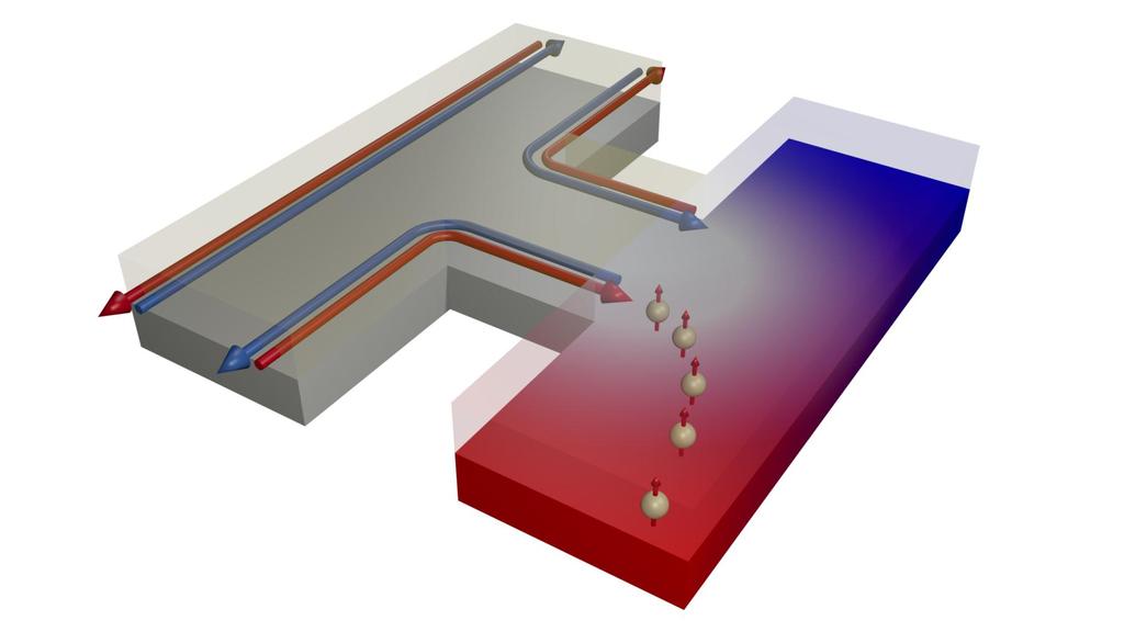
24 A two-dimensional topological insulator B = 0 Quantum Spin Hall State helical edge states invariant under time reversal consisting of two counter propagating spin polarized edge channels and an insulating bulk the required magnetic field can be provided by the intrinsic spin orbit interaction
25 Protected Edge States suppressed backscattering: deflection into the bulk is not possible, because of the insulating bulk state
26 Protected Edge States suppressed backscattering: a deflection of 180 has to reverse momentum and spin spin reversion is possible in two different ways: acquired phase change: destructive interference Dj = 2
27 Stability of Helical Edge States Kramers Pairs, 1 k s k, s, 1 x 2e h 2 G QSHE x backscattering is only possible by time reversal symmetry breaking processes (for example external magnetic fields) or if more states are present k s k, s, 2 1, x x x x

28
29 Topological Insulator : A New B=0 Phase There are 2 classes of 2D time reversal invariant band structures Z 2 topological invariant: = 0,1 Edge States for 0<k</a =0 : Conventional Insulator =1 : Topological Insulator Kramers degeneracy at points with time reversal invariant momenta k* = k* + G k*=0 k*=/a k*=0 k*=/a even number of bands crossing Fermi energy odd number of bands crossing Fermi energy
30 3D Topological Insulator There are 4 surface Dirac Points due to Kramers degeneracy k y L 4 L 3 k x L 1 L 2 2D Dirac Point Surface Brillouin Zone 0 = 0 : Weak Topological Insulator E E k=l a k=l b OR k=l a k=l b How do the Dirac points connect? Determined by 4 bulk Z 2 topological invariants 0 ; ( ) k y Related to layered 2D QSHI ; ( ) ~ Miller indices Fermi surface encloses even number of Dirac points k x 0 = 1 : Strong Topological Insulator Fermi circle encloses odd number of Dirac points Topological Metal : 1/4 graphene Berry s phase Robust to disorder: impossible to localize k y k x E F

. Band Theory : H. Zhang et. al, Nature Phys. (2009). 0;(1,2,3) = 1;(000) : Band inversion at G Energy gap: D ~.")
31 3D Topological Insulator Bi 1-x Sb x Theory: Predict Bi 1-x Sb x is a topological insulator by exploiting inversion symmetry of pure Bi, Sb (Fu,Kane PRL 07) Experiment: ARPES (Hsieh et al. Nature 08) Bi 1-x Sb x is a Strong Topological Insulator 0 ;( 1, 2, 3 ) = 1;(111) 5 surface state bands cross E F between G and M Bi 2 Se 3 ARPES Experiment : Y. Xia et al., Nature Phys. (2009). Band Theory : H. Zhang et. al, Nature Phys. (2009). 0;(1,2,3) = 1;(000) : Band inversion at G Energy gap: D ~.3 ev : A room temperature topological insulator Simple surface state structure : Similar to graphene, except only a single Dirac point E F
32 QSHE in Graphene Graphene edge states gap C.L.Kane and E.J.Mele, PRL 95, (2005) Graphene spin-orbit coupling strength is too weak gap only about 30 ev. not accessible in experiments
 E1 0 k B.A Bernevig, T.L. Hughes, S.C.")
33 QSHE in HgTe Helical edge states for inverted HgTe QW E H1 DEg = mev (typically) E1 0 k B.A Bernevig, T.L. Hughes, S.C. Zhang, Science 314, 1757 (2006)


34 Effective Tight Binding Model preserves TRS TKKN invariant zero Hall conductivity quantized spin Hall conductivity n n n n n s 2 n
35 Effective Tight Binding Model square lattice with 4 orbitals per site s,, s,, ( p ip ),, ( p ip ), x y x y nearest neighbor hopping integral basis: E1, H1, E1, H1 H ( k, k ) eff x y hk ( ) 0 * 0 h ( k)
 h( k) A 2 M ( k) k Asin k sin x i kx sin kx isin kx M ( k) k 2 at the G-point k 0 A k M ( k) Ak x ik x x ik x M ( k) relativistic Dirac equation M 0 normal QW for M 0 inverted QW with tunable")
36 Effective Tight Binding Model square lattice with 4 orbitals per site s,, s,, ( p ip ),, ( p ip ), x y x y nearest neighbor hopping integral basis: E1, H1, E1, H1 H ( k, k ) eff x y hk ( ) 0 * 0 h ( k) h( k) A 2 M ( k) k Asin k sin x i kx sin kx isin kx M ( k) k 2 at the G-point k 0 A k M ( k) Ak x ik x x ik x M ( k) relativistic Dirac equation M 0 normal QW for M 0 inverted QW with tunable parameter M (band-gap)
 E 4.0nm 6.2 nm 7.")
37 Bandstructure HgTe B.A Bernevig, T.L. Hughes, S.C. Zhang, Science 314, 1757 (2006) E 4.0nm 6.2 nm 7.0 nm k E1 H1 normal gap H1 E1 inverted gap

38 Bandstructure HgTe edge states for M > 0 M < 0 B.A Bernevig, T.L. Hughes, S.C. Zhang, Science 314, 1757 (2006) states with linear dispersion


39 Quantum Spin Hall Effect M > 0 M < 0 normal insulator QSHE bulk entire sample insulating bulk insulating
40 Mass domain wall inverted band structure E H1 E1 0 k states localized on the domain wall which disperse along the x-direction y M>0 M<0 y M>0 x M<0 0 M x M>0 helical edge states
41 Summary
42
 7 band inversion D.J. Chadi et al.")
43 HgTe band structure 1000 semi-metal or topological metal 500 E (mev) D 8 6 E g k (0.01 ) 7 band inversion D.J. Chadi et al. PRB, 3058 (1972) 6 8 E G E G 300 mev
44 CdTe and HgTe CdTe HgTe H = H 1 + H D + H mv + H so
 8 6 7 How to open the bulk band gap? 1. quantum confinement 2D TI 2. strain 3D TI")
45 HgTe Semi-metal with bulk band inversion 1000 E (mev) k (0.01 ) How to open the bulk band gap? 1. quantum confinement 2D TI 2. strain 3D TI

46


47 Quantum Well Structures E E g2 E g1 quantized energy levels in z-direction z (growth direction) x y quasi free electron gas in the xy-plane

48 MBE Quantum Well Growth by Molecular Beam Epitaxy QW


49 MBE Cluster at Würzburg

50 MBE Integrated in UHV transport system with 6 chambers Riber 3200 MBE Horizontal system 8 cell ports Maximum substrate dimension 2 wavers Pumped by a kryo pump, three nitrogen coldshields and a Tisublimation pump
51 HgTe Quantum Wells MBE-Growth 6.0 Bandgap vs. lattice constant (at room temperature in zinc blende structure) Bandgap energy (ev) lattice constant a [Å] 0 CT-CREW 1999


52 HgTe Quantum Wells free electron gas in the QW by donor doping of the barriers
53 HgTe Quantum Well Structures layer structure Carrier densities: n s = 1 x x cm -2 Carrier mobilities: = 1 x x 10 6 cm 2 /Vs gate insulator cap layer doping layer barrier quantum well barrier doping layer buffer substrate Au 100 nm Si N /SiO nm HgCdTe x = nm HgCdTe x = nm HgCdTe with I 10 nm HgCdTe x = nm HgTe 10 nm HgCdTe x = nm HgCdTe with I 10 nm HgCdTe x = nm CdTe CdZnTe(001) symmetric or asymmetric doping
54 E / mev n to p Transitions H1 n max = 1.35 x cm H2 p max = 3.2 x cm E ,0 0,1 0,2 0,3 0,4 0,5 k / nm -1 gate insulator cap layer doping layer barrier quantum well barrier doping layer buffer substrate Au 100 nm Si3N 4/SiO2 25 nm CdTe 10 nm HgCdTe x = nm HgCdTe with I 10 nm HgCdTe x = nm HgTe 10 nm HgCdTe x = nm HgCdTe with I 10 nm HgCdTe x = nm CdTe CdZnTe(001) R xy / Q nm QW T = 1.5 K 0V V Gate B / T -2V +5V +5,0 V +4,5 V +4,0 V +3,5 V +3,0 V +2,5 V +2,0 V +1,5 V +1,0 V +0,5 V 0 V -2,0 V
55 E (mev) E (mev) HgTe-Quantum Wells QW Barrier 1000 HgTe Hg 0.32 Cd 0.68 Te VBO k (0.01 ) 7 7 k (0.01 )
56 HgTe-Quantum Wells Typ-III QW d E (mev) k (0.01 ) G 6 HgCdTe HgTe G 8 HH1 E1 LH1 inverted band structure HgCdTe
 Zero Gap for 6.3 nm QW structures B. Büttner et al.")
57 Bandstructure G 6 HgTe HgCdTe G 6 HgTe HgCdTe G 8 G 8 B.A Bernevig et al., Science 314, 1757 (2006) Zero Gap for 6.3 nm QW structures B. Büttner et al., Nature Physics 7, 418 (2011)
![E [mev] E [mev] Dirac Band Structure 80 E2 d c 40](/docs-images/81/83321508/images/58-1.jpg "E1 0 H1-40 H2 H3-80 H4 4 6 8 10 d [nm] 12 14 100 50")
=(1,1) -100 H2 0.0 0.1 0.2 0.3 0.4 0.")
58 E [mev] E [mev] Dirac Band Structure 80 E2 d c 40 E1 0 H1-40 H2 H3-80 H d [nm] E1 H1 in-plane direction (k x,k y )=(1,0) (k x,k y )=(1,1) -100 H k [nm -1 ]
59 xx [ xx [ Zero Gap B = 1 T 80k 70k 7 6 B = 5 T 3k s xy [e²/h] k 50k 40k 30k 20k s xy [e²/h] k 1k 0 10k -1-0,5 0,0 0,5 1,0 V G - V Dirac [V] V G - V Dirac [V] 0 B. Büttner et al., Nature Physics 7, 418 (2011)
 conversion taken from appropriate Kane model B. Büttner et al.")
60 LL-Dispersion Kane model effective model LLchart Parameters: M ~ 0 ( mev) D = mev nm² G = mev nm² A = mev nm E(VG) conversion taken from appropriate Kane model B. Büttner et al., Nature Physics 7, 418 (2011)
61
62 x G 2e h 2 x
63 Experiment e e k k
64 Small Samples L W (L x W) m 2.0 x 1.0 m 1.0 x 1.0 m 1.0 x 0.5 m
65 QSHE Size Dependence 10 6 (1 x 1) m 2 non-inverted R xx / (2 x 1) m 2 (1 x 1) m 2 G = 2 e 2 /h 10 3 (1 x 0.5) m (V Gate - V thr ) / V König et al., Science 318, 766 (2007)


66 m 2 m 6 5 4
67 Conductance Quantization in 4-terminal geometry!? 20 V R xx / k G = 2 e 2 /h I (V Gate - V thr ) / V
68 Small Samples
69 Role of Ohmic Contacts n-type metallic contact areas and leads areas where scattering takes place spin relaxation
70 Multi-Terminal Probe T t t I e G h I e G h generally ) ( e h n R t 3 exp 4 2 t t R R h e G t 2,exp 4 2 Landauer-Büttiker Formalism normal conducting contacts no QSHE ji j ij i ii i i T R M h e I 2
71 QSHE in inverted HgTe-QWs G = 2/3 e 2 /h V I V R xx (k I 5 4 G = 2 e 2 /h 10 5 (1 x 0.5) m (V Gate - V thr ) (V) (2 x 1) m 2 R R 2t 4t 3
72 I (na) Rnl (k) Non-locality I: 1-4 V nl :2-3 V V 3 I mk U Gate [ V ] A. Roth, HB et al., Science 325,295 (2009)
73 R (k) Non-locality I: 1-3 V nl : LB: 8.6 k 12 V 10 8 G=3 e 2 /h 4-terminal V* (V) A. Roth, HB et al., Science 325,295 (2009)

74 Non-locality 1 2 I: 1-4 V nl :2-3 V LB: 6.4 k 5 G=4 e 2 /h R 14,23 / k V gate / V A. Roth, HB et al., Science 325,295 (2009)
75 R nl (k) Non-locality V LB: 4.3 k ,0-5,5-5,0-4,5-4,0-3,5-3,0 V (V) A. Roth, HB et al., Science 325,295 (2009)
76 Back Scattering potential fluctuations introduce areas of normal metallic (n- or p-) conductance in which back scattering becomes possible QSHE The potential landscape is modified by gate (density) sweeps!

77 Back Scattering area of raised or lowered chem. Pot. the probalility for back scatterring increases strength length additional ohmic contact transition from a two to a three terminal device
78 Additional Scattering Potential Transition from scattering strength 2 e 2 /h 3/2 e 2 /h A. Roth, HB et al., Science 325,295 (2009)

79 Additional Scattering Potential R 14,23 / k V gate / V A. Roth, HB et al., Science 325,295 (2009)
80 Rnl (kw) Potential Fluctuations V LB: 4.3 k one additional contact: between 2 and k 4 3 V x A. Roth, HB et al., Science 325,295 (2009)
81 V Potential Fluctuations different gate sweep direction V x LB: 22.1 k R nl / k LB: 12.9 k V g / V Hysteresis effects due to charging of trap states at the SC-insulator interface J. Hinz, HB et al., Semicond. Sci. Technol. 21 (2006)

 hysteresis effects: J. Hinz et al., Semicond. Sci.")
82 metal insulator QW HgTe Quantum Well Structures layer structure impurity states discharging charging gate insulator Au 100 nm Si N /SiO cap layer doping layer barrier quantum well barrier doping layer buffer substrate 25 nm HgCdTe x = nm HgCdTe x = nm HgCdTe with I 10 nm HgCdTe x = nm HgTe 10 nm HgCdTe x = nm HgCdTe with I 10 nm HgCdTe x = nm CdTe CdZnTe(001) hysteresis effects: J. Hinz et al., Semicond. Sci. Technol. 21 (2006)
83
84 Spin Polarizer 2D topological insulator attached to four metallic contacts/leads voltage contacts electron drain electron source
85 Spin Polarizer 2D topological insulator attached to four metallic contacts/leads 50% 1 : 4 50% electron drain electron source
86 Spin Polarizer 2D topological insulator attached to four metallic contacts/leads electron drain 100% 100 % 50% I = 0 electron drain 100% electron source
87 Spin Injector 2D topological insulator attached to four metallic contacts/leads 100% spin injection 100 % even with backscattering!
88 Spin Detection 100% D spin detection 100 %

89 Spin Manipulation D spin injection and spin manipulation by SO induced spin rotation (Rashba effect)

90 QSHE SHE

91 QSHE SHE QSHE Spin Hall Effect as creator and analyzer of spin polarized electrons SHE -1
92 Rashba Effect structural inversion asymmetry (SIA) Y.A. Bychkov and E.I. Rashba, JETP Lett. 39, 78 (1984); J. Phys. C 17, 6039 (1984): Rashba-Term: H R R s k s k x y y x B eff p E 2 2 k E Ei k * 2m (for electrons) 2 2 k E Ei k * 2m 3 (for holes)
93 Origin of the Spin-Hall Effect intrinsic B eff p E z E x 2DEG J.Sinova et al., Phys. Rev. Lett. 92, (2004)


94 intrinsic SHE Rashba and Spin-Hall Effect Rashba effect B eff p E

95 Split Gate H-Bar
96 QSHE Spin-Detector 5 4 QSHI-type detector R 34,12 / k 3 2 injector sweep V injector-gate / V x 0.04 QSHE n-type injector SHE x QSHI-type detector detector sweep 0.2 p-type injector V detector-gate / V
97 E / mev E / mev n-regime Q2198 p-regime n = cm -2 n H1 dl = cm -2 E1 H k / nm -1 E F p = cm -2 n dl = cm -2 H1 Dk E1 H k / nm -1 E F eex j s, y pf pf Dk 16m J.Sinova et al., Phys. Rev. Lett. 92, (2004) Intrinsic Spin Hall Effekt Nature Physics 6, 448 (2010)
98 QSHE Spin-Injector 5 4 QSHI-type injector R 12,34 / k 3 2 detector sweep V detector-gate / V x 0.04 QSHE n-type detector SHE x QSHI-type detector injector sweep 0.2 p-type detector

99 C. Brüne et al., Nature Physics, 8, 485 (2012)
Hartmut Buhmann. Physikalisches Institut, EP3 Universität Würzburg Germany
 Hartmut Buhmann Physikalisches Institut, EP3 Universität Würzburg Germany Outline Insulators and Topological Insulators HgTe quantum well structures Two-Dimensional TI Quantum Spin Hall Effect experimental
Spin-orbit Effects in Semiconductor Spintronics. Laurens Molenkamp Physikalisches Institut (EP3) University of Würzburg
 University of Würzburg") Spin-orbit Effects in Semiconductor Spintronics Laurens Molenkamp Physikalisches Institut (EP3) University of Würzburg Collaborators Hartmut Buhmann, Charlie Becker, Volker Daumer, Yongshen Gui Matthias
Spin-orbit Effects in Semiconductor Spintronics Laurens Molenkamp Physikalisches Institut (EP3) University of Würzburg Collaborators Hartmut Buhmann, Charlie Becker, Volker Daumer, Yongshen Gui Matthias
Topological insulators
 http://www.physik.uni-regensburg.de/forschung/fabian Topological insulators Jaroslav Fabian Institute for Theoretical Physics University of Regensburg Stara Lesna, 21.8.212 DFG SFB 689 what are topological
Topological Insulators
 Topological Insulators Aira Furusai (Condensed Matter Theory Lab.) = topological insulators (3d and 2d) Outline Introduction: band theory Example of topological insulators: integer quantum Hall effect
The Quantum Spin Hall Effect
 The Quantum Spin Hall Effect Shou-Cheng Zhang Stanford University with Andrei Bernevig, Taylor Hughes Science, 314,1757 2006 Molenamp et al, Science, 318, 766 2007 XL Qi, T. Hughes, SCZ preprint The quantum
Topological insulators
 Oddelek za fiziko Seminar 1 b 1. letnik, II. stopnja Topological insulators Author: Žiga Kos Supervisor: prof. dr. Dragan Mihailović Ljubljana, June 24, 2013 Abstract In the seminar, the basic ideas behind
What is a topological insulator? Ming-Che Chang Dept of Physics, NTNU
 What is a topological insulator? Ming-Che Chang Dept of Physics, NTNU A mini course on topology extrinsic curvature K vs intrinsic (Gaussian) curvature G K 0 G 0 G>0 G=0 K 0 G=0 G
Introduction to topological insulators. Jennifer Cano
 Introduction to topological insulators Jennifer Cano Adapted from Charlie Kane s Windsor Lectures: http://www.physics.upenn.edu/~kane/ Review article: Hasan & Kane Rev. Mod. Phys. 2010 What is an insulator?
Introductory lecture on topological insulators. Reza Asgari
 Introductory lecture on topological insulators Reza Asgari Workshop on graphene and topological insulators, IPM. 19-20 Oct. 2011 Outlines -Introduction New phases of materials, Insulators -Theory quantum
Notes on Topological Insulators and Quantum Spin Hall Effect. Jouko Nieminen Tampere University of Technology.
 Notes on Topological Insulators and Quantum Spin Hall Effect Jouko Nieminen Tampere University of Technology. Not so much discussed concept in this session: topology. In math, topology discards small details
Topological insulator (TI)
") Topological insulator (TI) Haldane model: QHE without Landau level Quantized spin Hall effect: 2D topological insulators: Kane-Mele model for graphene HgTe quantum well InAs/GaSb quantum well 3D topological
Topological insulator (TI) Haldane model: QHE without Landau level Quantized spin Hall effect: 2D topological insulators: Kane-Mele model for graphene HgTe quantum well InAs/GaSb quantum well 3D topological
Topological Physics in Band Insulators II
 Topological Physics in Band Insulators II Gene Mele University of Pennsylvania Topological Insulators in Two and Three Dimensions The canonical list of electric forms of matter is actually incomplete Conductor
Basics of topological insulator
 011/11/18 @ NTU Basics of topological insulator Ming-Che Chang Dept of Physics, NTNU A brief history of insulators Band insulator (Wilson, Bloch) Mott insulator Anderson insulator Quantum Hall insulator
Topological Insulators
 Topological Insulators A new state of matter with three dimensional topological electronic order L. Andrew Wray Lawrence Berkeley National Lab Princeton University Surface States (Topological Order in
Topological Insulators and Superconductors
 Topological Insulators and Superconductors Lecture #1: Topology and Band Theory Lecture #: Topological Insulators in and 3 dimensions Lecture #3: Topological Superconductors, Majorana Fermions an Topological
InAs/GaSb A New 2D Topological Insulator
 InAs/GaSb A New 2D Topological Insulator 1. Old Material for New Physics 2. Quantized Edge Modes 3. Adreev Reflection 4. Summary Rui-Rui Du Rice University Superconductor Hybrids Villard de Lans, France
Effective Field Theories of Topological Insulators
 Effective Field Theories of Topological Insulators Eduardo Fradkin University of Illinois at Urbana-Champaign Workshop on Field Theoretic Computer Simulations for Particle Physics and Condensed Matter
Topological insulators. Pavel Buividovich (Regensburg)
") Topological insulators Pavel Buividovich (Regensburg) Hall effect Classical treatment Dissipative motion for point-like particles (Drude theory) Steady motion Classical Hall effect Cyclotron frequency
Topological insulators Pavel Buividovich (Regensburg) Hall effect Classical treatment Dissipative motion for point-like particles (Drude theory) Steady motion Classical Hall effect Cyclotron frequency
Topological insulator with time-reversal symmetry
 Phys620.nb 101 7 Topological insulator with time-reversal symmetry Q: Can we get a topological insulator that preserves the time-reversal symmetry? A: Yes, with the help of the spin degree of freedom.
Time Reversal Invariant Ζ 2 Topological Insulator
 Time Reversal Invariant Ζ Topological Insulator D Bloch Hamiltonians subject to the T constraint 1 ( ) ΘH Θ = H( ) with Θ = 1 are classified by a Ζ topological invariant (ν =,1) Understand via Bul-Boundary
Topological insulators and the quantum anomalous Hall state. David Vanderbilt Rutgers University
 Topological insulators and the quantum anomalous Hall state David Vanderbilt Rutgers University Outline Berry curvature and topology 2D quantum anomalous Hall (QAH) insulator TR-invariant insulators (Z
Topological Insulators and Superconductors. Tokyo 2010 Shoucheng Zhang, Stanford University
 Topological Insulators and Superconductors Tokyo 2010 Shoucheng Zhang, Stanford University Colloborators Stanford group: Xiaoliang Qi, Andrei Bernevig, Congjun Wu, Chaoxing Liu, Taylor Hughes, Sri Raghu,
Organizing Principles for Understanding Matter
 Organizing Principles for Understanding Matter Symmetry Conceptual simplification Conservation laws Distinguish phases of matter by pattern of broken symmetries Topology Properties insensitive to smooth
5 Topological insulator with time-reversal symmetry
 Phys62.nb 63 5 Topological insulator with time-reversal symmetry It is impossible to have quantum Hall effect without breaking the time-reversal symmetry. xy xy. If we want xy to be invariant under, xy
Quantum Hall effect. Quantization of Hall resistance is incredibly precise: good to 1 part in I believe. WHY?? G xy = N e2 h.
 Quantum Hall effect V1 V2 R L I I x = N e2 h V y V x =0 G xy = N e2 h n.b. h/e 2 = 25 kohms Quantization of Hall resistance is incredibly precise: good to 1 part in 10 10 I believe. WHY?? Robustness Why
InAs/GaSb A New Quantum Spin Hall Insulator
 InAs/GaSb A New Quantum Spin Hall Insulator Rui-Rui Du Rice University 1. Old Material for New Physics 2. Quantized Edge Modes 3. Andreev Reflection 4. Summary KITP Workshop on Topological Insulator/Superconductor
Symmetry, Topology and Phases of Matter
 Symmetry, Topology and Phases of Matter E E k=λ a k=λ b k=λ a k=λ b Topological Phases of Matter Many examples of topological band phenomena States adiabatically connected to independent electrons: - Quantum
Quantum Spin Hall Insulator State in HgTe Quantum Wells
 SLAC-PUB-15949 Quantum Spin Hall Insulator State in HgTe Quantum Wells Markus König 1, Steffen Wiedmann 1, Christoph Brüne 1, Andreas Roth 1, Hartmut Buhmann 1, Laurens W. Molenkamp 1,, Xiao-Liang Qi 2
Les états de bord d un. isolant de Hall atomique
 Les états de bord d un isolant de Hall atomique séminaire Atomes Froids 2/9/22 Nathan Goldman (ULB), Jérôme Beugnon and Fabrice Gerbier Outline Quantum Hall effect : bulk Landau levels and edge states
arxiv: v1 [cond-mat.other] 20 Apr 2010
![arxiv: v1 [cond-mat.other] 20 Apr 2010](/thumbs/93/114512366.jpg "arxiv: v1 [cond-mat.other] 20 Apr 2010") Characterization of 3d topological insulators by 2d invariants Rahul Roy Rudolf Peierls Centre for Theoretical Physics, 1 Keble Road, Oxford, OX1 3NP, UK arxiv:1004.3507v1 [cond-mat.other] 20 Apr 2010
Characterization of 3d topological insulators by 2d invariants Rahul Roy Rudolf Peierls Centre for Theoretical Physics, 1 Keble Road, Oxford, OX1 3NP, UK arxiv:1004.3507v1 [cond-mat.other] 20 Apr 2010
ARPES experiments on 3D topological insulators. Inna Vishik Physics 250 (Special topics: spectroscopies of quantum materials) UC Davis, Fall 2016
 UC Davis, Fall 2016") ARPES experiments on 3D topological insulators Inna Vishik Physics 250 (Special topics: spectroscopies of quantum materials) UC Davis, Fall 2016 Outline Using ARPES to demonstrate that certain materials
ARPES experiments on 3D topological insulators Inna Vishik Physics 250 (Special topics: spectroscopies of quantum materials) UC Davis, Fall 2016 Outline Using ARPES to demonstrate that certain materials
Physics of Semiconductors
 Physics of Semiconductors 13 th 2016.7.11 Shingo Katsumoto Department of Physics and Institute for Solid State Physics University of Tokyo Outline today Laughlin s justification Spintronics Two current
Topological Defects inside a Topological Band Insulator
 Topological Defects inside a Topological Band Insulator Ashvin Vishwanath UC Berkeley Refs: Ran, Zhang A.V., Nature Physics 5, 289 (2009). Hosur, Ryu, AV arxiv: 0908.2691 Part 1: Outline A toy model of
Spin Hall and quantum spin Hall effects. Shuichi Murakami Department of Physics, Tokyo Institute of Technology PRESTO, JST
 YKIS2007 (Kyoto) Nov.16, 2007 Spin Hall and quantum spin Hall effects Shuichi Murakami Department of Physics, Tokyo Institute of Technology PRESTO, JST Introduction Spin Hall effect spin Hall effect in
Symmetries in Quantum Transport : From Random Matrix Theory to Topological Insulators. Philippe Jacquod. U of Arizona
 Symmetries in Quantum Transport : From Random Matrix Theory to Topological Insulators Philippe Jacquod U of Arizona UA Phys colloquium - feb 1, 2013 Continuous symmetries and conservation laws Noether
Spin orbit interaction in graphene monolayers & carbon nanotubes
 Spin orbit interaction in graphene monolayers & carbon nanotubes Reinhold Egger Institut für Theoretische Physik, Düsseldorf Alessandro De Martino Andreas Schulz, Artur Hütten MPI Dresden, 25.10.2011 Overview
Lecture notes on topological insulators
 Lecture notes on topological insulators Ming-Che Chang Department of Physics, National Taiwan Normal University, Taipei, Taiwan (Dated: November 1, 18) Contents I. D Topological insulator 1 A. General
Topological Insulator Surface States and Electrical Transport. Alexander Pearce Intro to Topological Insulators: Week 11 February 2, / 21
 Topological Insulator Surface States and Electrical Transport Alexander Pearce Intro to Topological Insulators: Week 11 February 2, 2017 1 / 21 This notes are predominately based on: J.K. Asbóth, L. Oroszlány
Quantum anomalous Hall states on decorated magnetic surfaces
 Quantum anomalous Hall states on decorated magnetic surfaces David Vanderbilt Rutgers University Kevin Garrity & D.V. Phys. Rev. Lett.110, 116802 (2013) Recently: Topological insulators (TR-invariant)
Local currents in a two-dimensional topological insulator
 Local currents in a two-dimensional topological insulator Xiaoqian Dang, J. D. Burton and Evgeny Y. Tsymbal Department of Physics and Astronomy Nebraska Center for Materials and Nanoscience University
Graphene and Carbon Nanotubes
 Graphene and Carbon Nanotubes 1 atom thick films of graphite atomic chicken wire Novoselov et al - Science 306, 666 (004) 100μm Geim s group at Manchester Novoselov et al - Nature 438, 197 (005) Kim-Stormer
Laurens W. Molenkamp. Physikalisches Institut, EP3 Universität Würzburg
 Laurens W. Molenkamp Physikalisches Institut, EP3 Universität Würzburg Overview - HgTe/CdTe bandstructure, quantum spin Hall effect: 2D TI - Dirac surface states of strained bulk HgTe: 3D TI - Topological
Quantum Spin Hall Effect: a theoretical and experimental introduction at kindergarten level, non-shown version
 Quantum Spin Hall Effect: a theoretical and experimental introduction at kindergarten level, non-shown version Ze-Yang Li 1, Jia-Chen Yu 2 and Shang-Jie Xue 3 December 21, 2015 1 光学所 2 凝聚态所 3 量 材料中 Historical
Graphite, graphene and relativistic electrons
 Graphite, graphene and relativistic electrons Introduction Physics of E. graphene Y. Andrei Experiments Rutgers University Transport electric field effect Quantum Hall Effect chiral fermions STM Dirac
3D Weyl metallic states realized in the Bi 1-x Sb x alloy and BiTeI. Heon-Jung Kim Department of Physics, Daegu University, Korea
 3D Weyl metallic states realized in the Bi 1-x Sb x alloy and BiTeI Heon-Jung Kim Department of Physics, Daegu University, Korea Content 3D Dirac metals Search for 3D generalization of graphene Bi 1-x
POEM: Physics of Emergent Materials
 POEM: Physics of Emergent Materials Nandini Trivedi L1: Spin Orbit Coupling L2: Topology and Topological Insulators Tutorials: May 24, 25 (2017) Scope of Lectures and Anchor Points: 1.Spin-Orbit Interaction
Disordered topological insulators with time-reversal symmetry: Z 2 invariants
 Keio Topo. Science (2016/11/18) Disordered topological insulators with time-reversal symmetry: Z 2 invariants Hosho Katsura Department of Physics, UTokyo Collaborators: Yutaka Akagi (UTokyo) Tohru Koma
Quantum Hall Effect in Graphene p-n Junctions
 Quantum Hall Effect in Graphene p-n Junctions Dima Abanin (MIT) Collaboration: Leonid Levitov, Patrick Lee, Harvard and Columbia groups UIUC January 14, 2008 Electron transport in graphene monolayer New
Topological Insulators and Ferromagnets: appearance of flat surface bands
 Topological Insulators and Ferromagnets: appearance of flat surface bands Thomas Dahm University of Bielefeld T. Paananen and T. Dahm, PRB 87, 195447 (2013) T. Paananen et al, New J. Phys. 16, 033019 (2014)
Physics of Semiconductors (Problems for report)
") Physics of Semiconductors (Problems for report) Shingo Katsumoto Institute for Solid State Physics, University of Tokyo July, 0 Choose two from the following eight problems and solve them. I. Fundamentals
Physics of Semiconductors (Problems for report) Shingo Katsumoto Institute for Solid State Physics, University of Tokyo July, 0 Choose two from the following eight problems and solve them. I. Fundamentals
3D topological insulators and half- Heusler compounds
 3D topological insulators and half- Heusler compounds Ram Seshadri Materials Department, and Department of Chemistry and Biochemistry Materials Research Laboratory University of California, Santa Barbara
Floquet theory of photo-induced topological phase transitions: Application to graphene
 Floquet theory of photo-induced topological phase transitions: Application to graphene Takashi Oka (University of Tokyo) T. Kitagawa (Harvard) L. Fu (Harvard) E. Demler (Harvard) A. Brataas (Norweigian
Topological Physics in Band Insulators. Gene Mele DRL 2N17a
 Topological Physics in Band Insulators Gene Mele DRL 2N17a Electronic States of Matter Benjamin Franklin (University of Pennsylvania) That the Electrical Fire freely removes from Place to Place in and
v. Tε n k =ε n k T r T = r, T v T = r, I v I = I r I = v. Iε n k =ε n k Berry curvature: Symmetry Consideration n k = n k
 Berry curvature: Symmetry Consideration Time reversal (i.e. motion reversal) 1 1 T r T = r, T v T = v. Tε n k =ε n k n k = n k Inversion Symmetry: 1 1 I r I = r, I v I = v. Iε n k =ε n k n k = n k θ
Observation of neutral modes in the fractional quantum hall effect regime. Aveek Bid
 Observation of neutral modes in the fractional quantum hall effect regime Aveek Bid Department of Physics, Indian Institute of Science, Bangalore Nature 585 466 (2010) Quantum Hall Effect Magnetic field
From graphene to Z2 topological insulator
 From graphene to Z2 topological insulator single Dirac topological AL mass U U valley WL ordinary mass or ripples WL U WL AL AL U AL WL Rashba Ken-Ichiro Imura Condensed-Matter Theory / Tohoku Univ. Dirac
2D Materials with Strong Spin-orbit Coupling: Topological and Electronic Transport Properties
 2D Materials with Strong Spin-orbit Coupling: Topological and Electronic Transport Properties Artem Pulkin California Institute of Technology (Caltech), Pasadena, CA 91125, US Institute of Physics, Ecole
Spins and spin-orbit coupling in semiconductors, metals, and nanostructures
 B. Halperin Spin lecture 1 Spins and spin-orbit coupling in semiconductors, metals, and nanostructures Behavior of non-equilibrium spin populations. Spin relaxation and spin transport. How does one produce
Room temperature topological insulators
 Room temperature topological insulators Ronny Thomale Julius-Maximilians Universität Würzburg ERC Topolectrics SFB Tocotronics Synquant Workshop, KITP, UC Santa Barbara, Nov. 22 2016 Correlated electron
A Short Introduction to Topological Superconductors
 A Short Introduction to Topological Superconductors --- A Glimpse of Topological Phases of Matter Jyong-Hao Chen Condensed Matter Theory, PSI & Institute for Theoretical Physics, ETHZ Dec. 09, 2015 @ Superconductivity
Minimal Update of Solid State Physics
 Minimal Update of Solid State Physics It is expected that participants are acquainted with basics of solid state physics. Therefore here we will refresh only those aspects, which are absolutely necessary
Berry s phase in Hall Effects and Topological Insulators
 Lecture 6 Berry s phase in Hall Effects and Topological Insulators Given the analogs between Berry s phase and vector potentials, it is not surprising that Berry s phase can be important in the Hall effect.
POEM: Physics of Emergent Materials
 POEM: Physics of Emergent Materials Nandini Trivedi L1: Spin Orbit Coupling L2: Topology and Topological Insulators Reference: Bernevig Topological Insulators and Topological Superconductors Tutorials:
First-Principles Calculation of Topological Invariants (Wannier Functions Approach) Alexey A. Soluyanov
 Alexey A. Soluyanov") First-Principles Calculation of Topological Invariants (Wannier Functions Approach) Alexey A. Soluyanov ES'12, WFU, June 8, 212 The present work was done in collaboration with David Vanderbilt Outline:
First-Principles Calculation of Topological Invariants (Wannier Functions Approach) Alexey A. Soluyanov ES'12, WFU, June 8, 212 The present work was done in collaboration with David Vanderbilt Outline:
Energy Spectrum and Broken spin-surface locking in Topological Insulator quantum dots
 Energy Spectrum and Broken spin-surface locking in Topological Insulator quantum dots A. Kundu 1 1 Heinrich-Heine Universität Düsseldorf, Germany The Capri Spring School on Transport in Nanostructures
Topological Kondo Insulator SmB 6. Tetsuya Takimoto
 Topological Kondo Insulator SmB 6 J. Phys. Soc. Jpn. 80 123720, (2011). Tetsuya Takimoto Department of Physics, Hanyang University Collaborator: Ki-Hoon Lee (POSTECH) Content 1. Introduction of SmB 6 in-gap
Lecture 20: Semiconductor Structures Kittel Ch 17, p , extra material in the class notes
 Lecture 20: Semiconductor Structures Kittel Ch 17, p 494-503, 507-511 + extra material in the class notes MOS Structure Layer Structure metal Oxide insulator Semiconductor Semiconductor Large-gap Semiconductor
Konstantin Y. Bliokh, Daria Smirnova, Franco Nori. Center for Emergent Matter Science, RIKEN, Japan. Science 348, 1448 (2015)
") Konstantin Y. Bliokh, Daria Smirnova, Franco Nori Center for Emergent Matter Science, RIKEN, Japan Science 348, 1448 (2015) QSHE and topological insulators The quantum spin Hall effect means the presence
Konstantin Y. Bliokh, Daria Smirnova, Franco Nori Center for Emergent Matter Science, RIKEN, Japan Science 348, 1448 (2015) QSHE and topological insulators The quantum spin Hall effect means the presence
Two Dimensional Chern Insulators, the Qi-Wu-Zhang and Haldane Models
 Two Dimensional Chern Insulators, the Qi-Wu-Zhang and Haldane Models Matthew Brooks, Introduction to Topological Insulators Seminar, Universität Konstanz Contents QWZ Model of Chern Insulators Haldane
SUPPLEMENTARY INFORMATION
 A Dirac point insulator with topologically non-trivial surface states D. Hsieh, D. Qian, L. Wray, Y. Xia, Y.S. Hor, R.J. Cava, and M.Z. Hasan Topics: 1. Confirming the bulk nature of electronic bands by
Electron spins in nonmagnetic semiconductors
 Electron spins in nonmagnetic semiconductors Yuichiro K. Kato Institute of Engineering Innovation, The University of Tokyo Physics of non-interacting spins Optical spin injection and detection Spin manipulation
Nanomaterials Characterization by lowtemperature Scanning Probe Microscopy
 Nanomaterials Characterization by lowtemperature Scanning Probe Microscopy Stefan Heun NEST, Istituto Nanoscienze-CNR and Scuola Normale Superiore Piazza San Silvestro 12, 56127 Pisa, Italy e-mail: stefan.heun@nano.cnr.it
Topological thermoelectrics
 Topological thermoelectrics JAIRO SINOVA Texas A&M University Institute of Physics ASCR Oleg Tretiakov, Artem Abanov, Suichi Murakami Great job candidate MRS Spring Meeting San Francisco April 28th 2011
Exploring topological states with cold atoms and photons
 Exploring topological states with cold atoms and photons Theory: Takuya Kitagawa, Dima Abanin, Erez Berg, Mark Rudner, Liang Fu, Takashi Oka, Immanuel Bloch, Eugene Demler Experiments: I. Bloch s group
Recent developments in topological materials
 Recent developments in topological materials NHMFL Winter School January 6, 2014 Joel Moore University of California, Berkeley, and Lawrence Berkeley National Laboratory Berkeley students: Andrew Essin,
Quantum Condensed Matter Physics Lecture 17
 Quantum Condensed Matter Physics Lecture 17 David Ritchie http://www.sp.phy.cam.ac.uk/drp/home 17.1 QCMP Course Contents 1. Classical models for electrons in solids. Sommerfeld theory 3. From atoms to
Visualizing Electronic Structures of Quantum Materials By Angle Resolved Photoemission Spectroscopy (ARPES)
") Visualizing Electronic Structures of Quantum Materials By Angle Resolved Photoemission Spectroscopy (ARPES) PART A: ARPES & Application Yulin Chen Oxford University / Tsinghua University www.arpes.org.uk
Visualizing Electronic Structures of Quantum Materials By Angle Resolved Photoemission Spectroscopy (ARPES) PART A: ARPES & Application Yulin Chen Oxford University / Tsinghua University www.arpes.org.uk
Topological Properties of Quantum States of Condensed Matter: some recent surprises.
 Topological Properties of Quantum States of Condensed Matter: some recent surprises. F. D. M. Haldane Princeton University and Instituut Lorentz 1. Berry phases, zero-field Hall effect, and one-way light
Spin Superfluidity and Graphene in a Strong Magnetic Field
 Spin Superfluidity and Graphene in a Strong Magnetic Field by B. I. Halperin Nano-QT 2016 Kyiv October 11, 2016 Based on work with So Takei (CUNY), Yaroslav Tserkovnyak (UCLA), and Amir Yacoby (Harvard)
Bloch, Landau, and Dirac: Hofstadter s Butterfly in Graphene. Philip Kim. Physics Department, Columbia University
 Bloch, Landau, and Dirac: Hofstadter s Butterfly in Graphene Philip Kim Physics Department, Columbia University Acknowledgment Prof. Cory Dean (now at CUNY) Lei Wang Patrick Maher Fereshte Ghahari Carlos
Three Most Important Topics (MIT) Today
 Today") Three Most Important Topics (MIT) Today Electrons in periodic potential Energy gap nearly free electron Bloch Theorem Energy gap tight binding Chapter 1 1 Electrons in Periodic Potential We now know the
Three Most Important Topics (MIT) Today Electrons in periodic potential Energy gap nearly free electron Bloch Theorem Energy gap tight binding Chapter 1 1 Electrons in Periodic Potential We now know the
2) Atom manipulation. Xe / Ni(110) Model: Experiment:
 Atom manipulation. Xe / Ni(110) Model: Experiment:") 2) Atom manipulation D. Eigler & E. Schweizer, Nature 344, 524 (1990) Xe / Ni(110) Model: Experiment: G.Meyer, et al. Applied Physics A 68, 125 (1999) First the tip is approached close to the adsorbate
2) Atom manipulation D. Eigler & E. Schweizer, Nature 344, 524 (1990) Xe / Ni(110) Model: Experiment: G.Meyer, et al. Applied Physics A 68, 125 (1999) First the tip is approached close to the adsorbate
Out-of-equilibrium electron dynamics in photoexcited topological insulators studied by TR-ARPES
 Cliquez et modifiez le titre Out-of-equilibrium electron dynamics in photoexcited topological insulators studied by TR-ARPES Laboratoire de Physique des Solides Orsay, France June 15, 2016 Workshop Condensed
Observation of topological surface state quantum Hall effect in an intrinsic three-dimensional topological insulator
 Observation of topological surface state quantum Hall effect in an intrinsic three-dimensional topological insulator Authors: Yang Xu 1,2, Ireneusz Miotkowski 1, Chang Liu 3,4, Jifa Tian 1,2, Hyoungdo
Topological states of matter in correlated electron systems
 Seminar @ Tsinghua, Dec.5/2012 Topological states of matter in correlated electron systems Qiang-Hua Wang National Lab of Solid State Microstructures, Nanjing University, Nanjing 210093, China Collaborators:Dunghai
TOPOLOGICAL BANDS IN GRAPHENE SUPERLATTICES
 TOPOLOGICAL BANDS IN GRAPHENE SUPERLATTICES 1) Berry curvature in superlattice bands 2) Energy scales for Moire superlattices 3) Spin-Hall effect in graphene Leonid Levitov (MIT) @ ISSP U Tokyo MIT Manchester
Kouki Nakata. University of Basel. KN, S. K. Kim (UCLA), J. Klinovaja, D. Loss (2017) arxiv:
, J. Klinovaja, D. Loss (2017) arxiv:") Magnon Transport Both in Ferromagnetic and Antiferromagnetic Insulating Magnets Kouki Nakata University of Basel KN, S. K. Kim (UCLA), J. Klinovaja, D. Loss (2017) arxiv:1707.07427 See also review article
Magnon Transport Both in Ferromagnetic and Antiferromagnetic Insulating Magnets Kouki Nakata University of Basel KN, S. K. Kim (UCLA), J. Klinovaja, D. Loss (2017) arxiv:1707.07427 See also review article
Weyl semi-metal: a New Topological State in Condensed Matter
 Weyl semi-metal: a New Topological State in Condensed Matter Sergey Savrasov Department of Physics, University of California, Davis Xiangang Wan Nanjing University Ari Turner and Ashvin Vishwanath UC Berkeley
Spatially resolved study of backscattering in the quantum spin Hall state SUPPLEMENTAL MATERIAL
 Spatially resolved study of backscattering in the quantum spin Hall state SUPPLEMENTAL MATERIAL Markus König 1,2, Matthias Baenninger 1,2, Andrei G. F. Garcia 1, Nahid Harjee 3, Beth L. Pruitt 4, C. Ames
LCI -birthplace of liquid crystal display. May, protests. Fashion school is in top-3 in USA. Clinical Psychology program is Top-5 in USA
 LCI -birthplace of liquid crystal display May, 4 1970 protests Fashion school is in top-3 in USA Clinical Psychology program is Top-5 in USA Topological insulators driven by electron spin Maxim Dzero Kent
Protected/non-protected edge states in two-dimensional lattices
 Protected/non-protected edge states in two-dimensional lattices (a review of edge states behavior) A. Aldea, M. Niţa and B. Ostahie National Institute of Materials Physics Bucharest-Magurele, Romania MESO-III,
Quantum Spin Hall Effect in Inverted Type II Semiconductors
 Quantum Spin Hall Effect in Inverted Type II Semiconductors Chaoxing Liu 1,2, Taylor L. Hughes 2, Xiao-Liang Qi 2, Kang Wang 3 and Shou-Cheng Zhang 2 1 Center for Advanced Study, Tsinghua University,Beijing,
Basic cell design. Si cell
 Basic cell design Si cell 1 Concepts needed to describe photovoltaic device 1. energy bands in semiconductors: from bonds to bands 2. free carriers: holes and electrons, doping 3. electron and hole current:
Topological Heterostructures by Molecular Beam Epitaxy
 Topological Heterostructures by Molecular Beam Epitaxy Susanne Stemmer Materials Department, University of California, Santa Barbara Fine Lecture, Northwestern University February 20, 2018 Stemmer Group
SUPPLEMENTARY INFORMATION
 DOI: 1.138/NMAT3449 Topological crystalline insulator states in Pb 1 x Sn x Se Content S1 Crystal growth, structural and chemical characterization. S2 Angle-resolved photoemission measurements at various
The Quantum Hall Effect
 The Quantum Hall Effect David Tong (And why these three guys won last week s Nobel prize) Trinity Mathematical Society, October 2016 Electron in a Magnetic Field B mẍ = eẋ B x = v cos!t! y = v sin!t!!
Scanning gate microscopy and individual control of edge-state transmission through a quantum point contact
 Scanning gate microscopy and individual control of edge-state transmission through a quantum point contact Stefan Heun NEST, CNR-INFM and Scuola Normale Superiore, Pisa, Italy Coworkers NEST, Pisa, Italy:
Quantum Confinement in Graphene
 Quantum Confinement in Graphene from quasi-localization to chaotic billards MMM dominikus kölbl 13.10.08 1 / 27 Outline some facts about graphene quasibound states in graphene numerical calculation of
Emergent topological phenomena in antiferromagnets with noncoplanar spins
 Emergent topological phenomena in antiferromagnets with noncoplanar spins - Surface quantum Hall effect - Dimensional crossover Bohm-Jung Yang (RIKEN, Center for Emergent Matter Science (CEMS), Japan)
Topological Insulators: Electronic structure, material systems and its applications
 Network for Computational Nanotechnology UC Berkeley, Univ. of Illinois, Norfolk (NCN) State, Northwestern, Purdue, UTEP Topological Insulators: Electronic structure, material systems and its applications