MPI Stuttgart. Atomic-scale control of graphene magnetism using hydrogen atoms. HiMagGraphene.
|
|
|
- Shon Freeman
- 6 years ago
- Views:
Transcription

1 MPI Stuttgart Atomic-scale control of graphene magnetism using hydrogen atoms HiMagGraphene Budapest, April, 2016


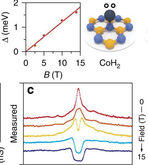
2 Magnetism in graphene: just remove a p z orbital Atomic Hydrogen π σ m T = m π = 1μ B (1.0 m B ) O. Yazyev, Rep. Prog. Phys (2010)
 m T = m π = 1μ B Spin Up QL (1.0 m Spin Down B ) Graphene H chemisorbs on Graphene 3 Adsorption Energy 0.")
3 Atomic Hydrogen on Monolayer Graphene DOS (au) Desorption energy (ev) Relaed Atomic structure Calculated spin density Magnetic moment = 1μ B spin density located on the opposite triangular sublattice. Simulated STM image (Tersoff-Hamann) m T = m π = 1μ B Spin Up QL (1.0 m Spin Down B ) Graphene H chemisorbs on Graphene 3 Adsorption Energy 0.9eV Distance of H atom over graphene (Å) Energy (ev) DFT calculations: M. Moaied, J.J Palacios, Feli Yndurain Spin Polarized DFT SIESTA code // (DZP) basis set.

4 Eperimental UHV-STM approach Illustration by Julio Gómez-Herrero
 Spin Up Spin Down Graphene m T = m π = 1μ B Theoretical")
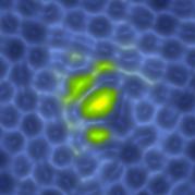
5 DOS (au) di/dv (a.u.) di/dv LDOS Starting point of the project! Spin-split peaks!! 20meV Atomic Hydrogen Voltage (mv) Spin Up Spin Down Graphene m T = m π = 1μ B Theoretical prediction Energy (ev)
 di/dv LDOS")


6 di/dv (a.u.) di/dv LDOS Proposed eperiments Spin-split peaks!! 20meV Voltage (mv)
 Coordinator (P1)")


7 The consortium (who we are) Coordinator (P1) Partner 2 Partner 3 P.I. co-investigator P.I. co-investigator P.I. MPI Stuttgart co-investigator I. Brihuega J.M.Gómez-Rodríguez J-Y Veuillen P. Mallet K. Kern M.Ternes Quasiparticle pseudospin BILAYER I Brihuega, P. Mallet, C. Bena, S. Bose, C. Michaelis, L. Vitali, F. Varchon, L.Magaud, K. Kern, J.Y. Veuillen Phys Rev. Lett. 101, (2008) 2.5Å MONOLAYER 2.5Å

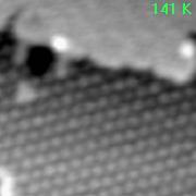
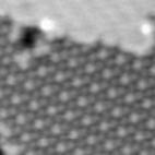
8 True variable Temperature eperiments 40 K T Point defects in graphene


")


9 Preparation of graphene substrates 4 th layer 3 rd layer 2 nd layer 1 st layer G/SiC-C doped twisted bi(tri)layer Gr 3232 nm² nm² Si C G/SiC-Si Neutral (thick) twisted multilayer ribbons on SiC samples 44 nm² Heavily doped ML and BL Gr Armchair edge 55 nm² Zig-Zag edge

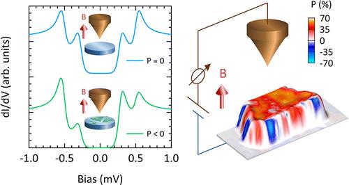
10 Magnetic Field dependence Spin polatization
11 Chronogram of activities: WP1. Substrate preparation and characterization (0-36) SiC(000-1): from ML to multilayer graphene; SiC(0001): ML and BL; HOPG; ML on BN/SiO 2 ; ML on SiO 2 ; ML graphene on (Au, Cu, Ir, Pt); graphene islands and ribbons on SiC. WP2. STS Characterization of H on undoped graphene (0-36) - LDOS of single H for different substrates - Spatial etension of the spin-split state - Interaction between graphene magnetic moments induced by neighboring H atoms WP3. Temperature dependent measurements (12-36) - Influence of thermal fluctuations in the magnetic moments - Dynamic evolution of H atoms. - Single and ensembles of H atoms WP4. Magnetic field dependence (6-36) - Proof of the magnetic origin of the peaks by using spin-sensitive tips - Observing the energy shifts due to the Zeeman energy - Determine the coupling strength and sign in ensembles of H atoms WP5. Spin manipulation (6-36) - Locally: using the STM tip to manipulate the H adsorption sites - Eternally: with doping (both by substrate and by gating) - On a device: try to inject spin polarized current without magnetic electrodes. time [months]
 12-36 WP3.")


12 Role of the partners (who does what) WP3. Temperature dependence WP1. Substrate preparation and characterization WP2. STS of H on undopped graphene WP4. Magnetic field dependence 6-36 Comprehensive characterization of H-induced graphene magnetism WP5. Spin manipulation
13 WP1: Enabling Research WP2: Spintronics
14 MPI Stuttgart HiMagGraphene Progress so far

15 Manipulating H magnetism
16 Manipulating H magnetism
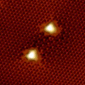
17 Manipulating H magnetism 7 H atoms up 7 H atoms up 7 H atoms down 7 H atoms down
18 Manipulating H magnetism 7 H atoms up 7 H atoms up 7 H atoms down 7 H atoms down
19 Manipulating H magnetism 7 H atoms up 7 H atoms down 7 H atoms down H. González-Herrero, J.M.Gómez-Rodríguez, P. Mallet, M. Moaied, J.J. Palacios, C. Salgado, M.M. Ugeda, J.Y. Veuillen, F. Ynduráin and I Brihuega, submitted


20 Manipulating H magnetism 7 H atoms up 7 H atoms down 7 H atoms up 7 H atoms down H. González-Herrero, J.M.Gómez-Rodríguez, P. Mallet, M. Moaied, J.J. Palacios, C. Salgado, M.M. Ugeda, J.Y. Veuillen, F. Ynduráin and I Brihuega, submitted
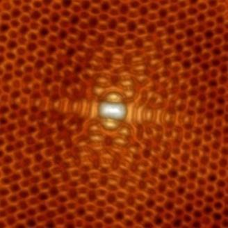
21 STM Sublattice localization of the polarized peak DFT H TOPOGRAPHY
22 E [mev] STM Sublattice localization of the polarized peak DFT LDOS (au) H -50 LDOS 1.95 V di/dv ( LDOS) mapping along the profile TOPOGRAPHY atom V Voltage (mv)
23 E [mev] STM Sublattice localization of the polarized peak DFT LDOS (au) PDOS (au) H -50 LDOS 1.95 V di/dv ( LDOS) mapping along the profile TOPOGRAPHY atom atom Spin up Spin Down atom DFT V Voltage (mv) Energy (ev) H. González-Herrero, J.M.Gómez-Rodríguez, P. Mallet, M. Moaied, J.J. Palacios, C. Salgado, M.M. Ugeda, J.Y. Veuillen, F. Ynduráin and I Brihuega, submitted

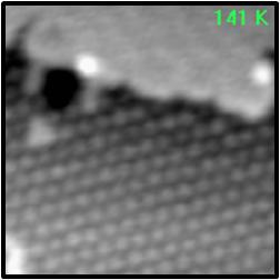
24 True variable Temperature eperiments 40 K 40 K T
Supporting Information for Ultra-narrow metallic armchair graphene nanoribbons
 Supporting Information for Ultra-narrow metallic armchair graphene nanoribbons Supplementary Figure 1 Ribbon length statistics. Distribution of the ribbon lengths and the fraction of kinked ribbons for
STM spectroscopy (STS)
") STM spectroscopy (STS) di dv 4 e ( E ev, r) ( E ) M S F T F Basic concepts of STS. With the feedback circuit open the variation of the tunneling current due to the application of a small oscillating voltage
STM spectroscopy (STS) di dv 4 e ( E ev, r) ( E ) M S F T F Basic concepts of STS. With the feedback circuit open the variation of the tunneling current due to the application of a small oscillating voltage
arxiv: v1 [cond-mat.mes-hall] 23 Dec 2011
![arxiv: v1 [cond-mat.mes-hall] 23 Dec 2011](/thumbs/83/87995118.jpg "arxiv: v1 [cond-mat.mes-hall] 23 Dec 2011") Electronic and structural characterization of divacancies in irradiated graphene Miguel M. Ugeda, 1, Iván Brihuega, 1 Fanny Hiebel, 2 Pierre Mallet, 2 Jean-Yves Veuillen, 2 José M. Gómez-Rodríguez, 1 and
Electronic and structural characterization of divacancies in irradiated graphene Miguel M. Ugeda, 1, Iván Brihuega, 1 Fanny Hiebel, 2 Pierre Mallet, 2 Jean-Yves Veuillen, 2 José M. Gómez-Rodríguez, 1 and
Self-assembly of molecules on surfaces. Manuel Alcamí Departamento de Química Universidad Autónoma de Madrid
 Self-assembly of molecules on surfaces Manuel Alcamí Departamento de Química Universidad Autónoma de Madrid Outline Outline Motivation Examples of molecules deposited on surfaces Graphene/Ru(0001) TQ /
Self-Assembly of Two-Dimensional Organic Networks Containing Heavy Metals (Pb, Bi) and Preparation of Spin-Polarized Scanning Tunneling Microscope
 and Preparation of Spin-Polarized Scanning Tunneling Microscope") MPhil Thesis Defense Self-Assembly of Two-Dimensional Organic Networks Containing Heavy Metals (Pb, Bi) and Preparation of Spin-Polarized Scanning Tunneling Microscope Presented by CHEN Cheng 12 th Aug.
MPhil Thesis Defense Self-Assembly of Two-Dimensional Organic Networks Containing Heavy Metals (Pb, Bi) and Preparation of Spin-Polarized Scanning Tunneling Microscope Presented by CHEN Cheng 12 th Aug.
Hydrogenated Graphene
 Hydrogenated Graphene Stefan Heun NEST, Istituto Nanoscienze-CNR and Scuola Normale Superiore Pisa, Italy Outline Epitaxial Graphene Hydrogen Chemisorbed on Graphene Hydrogen-Intercalated Graphene Outline
Tuning magnetic anisotropy, Kondo screening and Dzyaloshinskii-Moriya interaction in pairs of Fe adatoms
 Tuning magnetic anisotropy, Kondo screening and Dzyaloshinskii-Moriya interaction in pairs of Fe adatoms Department of Physics, Hamburg University, Hamburg, Germany SPICE Workshop, Mainz Outline Tune magnetic
Spatially resolving density-dependent screening around a single charged atom in graphene
 Supplementary Information for Spatially resolving density-dependent screening around a single charged atom in graphene Dillon Wong, Fabiano Corsetti, Yang Wang, Victor W. Brar, Hsin-Zon Tsai, Qiong Wu,
Physics of Nanotubes, Graphite and Graphene Mildred Dresselhaus
 Quantum Transport and Dynamics in Nanostructures The 4 th Windsor Summer School on Condensed Matter Theory 6-18 August 2007, Great Park Windsor (UK) Physics of Nanotubes, Graphite and Graphene Mildred
Microscopy and Spectroscopy with Tunneling Electrons STM. Sfb Kolloquium 23rd October 2007
 Microscopy and Spectroscopy with Tunneling Electrons STM Sfb Kolloquium 23rd October 2007 The Tunnel effect T ( E) exp( S Φ E ) Barrier width s Barrier heigth Development: The Inventors 1981 Development:
Outline. Introduction: graphene. Adsorption on graphene: - Chemisorption - Physisorption. Summary
 Outline Introduction: graphene Adsorption on graphene: - Chemisorption - Physisorption Summary 1 Electronic band structure: Electronic properties K Γ M v F = 10 6 ms -1 = c/300 massless Dirac particles!
Electronic states on the surface of graphite
 Electronic states on the surface of graphite Guohong Li, Adina Luican, Eva Y. Andrei * Department of Physics and Astronomy, Rutgers Univsersity, Piscataway, NJ 08854, USA Elsevier use only: Received date
Spin-orbit effects in graphene and graphene-like materials. Józef Barnaś
 Spin-orbit effects in graphene and graphene-like materials Józef Barnaś Faculty of Physics, Adam Mickiewicz University, Poznań & Institute of Molecular Physics PAN, Poznań In collaboration with: A. Dyrdał,
Optimizing Graphene Morphology on SiC(0001)
") Optimizing Graphene Morphology on SiC(0001) James B. Hannon Rudolf M. Tromp Graphene sheets Graphene sheets can be formed into 0D,1D, 2D, and 3D structures Chemically inert Intrinsically high carrier mobility
Optimizing Graphene Morphology on SiC(0001) James B. Hannon Rudolf M. Tromp Graphene sheets Graphene sheets can be formed into 0D,1D, 2D, and 3D structures Chemically inert Intrinsically high carrier mobility
Magnetic anisotropy in frustrated clusters and monolayers: Cr on triangular Au(111) surface
 surface") Magnetic anisotropy in frustrated clusters and monolayers: Cr on triangular Au(111) surface László Balogh Krisztián Palotás László Udvardi László Szunyogh Department of Theoretical Physics Budapest University
Magnetic anisotropy in frustrated clusters and monolayers: Cr on triangular Au(111) surface László Balogh Krisztián Palotás László Udvardi László Szunyogh Department of Theoretical Physics Budapest University
Scanning probe microscopy of graphene with a CO terminated tip
 Scanning probe microscopy of graphene with a CO terminated tip Andrea Donarini T. Hofmann, A. J. Weymouth, F. Gießibl 7.5.2014 - Theory Group Seminar The sample Single monolayer of graphene Epitaxial growth
Atomic-Scale Mapping of Thermoelectric Power on Graphene: Role of Defects and Boundaries
 1 Atomic-Scale Mapping of Thermoelectric Power on Graphene: Role of Defects and Boundaries Jewook Park 1, Guowei He 2, R. M. Feenstra 2, and An-Ping Li 1 1 Center for Nanophase Materials Sciences, Oak
From manipulation of the charge state to imaging of individual molecular orbitals and bond formation
 Scanning Probe Microscopy of Adsorbates on Insulating Films: From manipulation of the charge state to imaging of individual molecular orbitals and bond formation Gerhard Meyer, Jascha Repp, Peter Liljeroth
Site- and orbital-dependent charge donation and spin manipulation in electron-doped metal phthalocyanines
 Site- and orbital-dependent charge donation and spin manipulation in electron-doped metal phthalocyanines Cornelius Krull 1, Roberto Robles 2, Aitor Mugarza 1, Pietro Gambardella 1,3 1 Catalan Institute
Scanning Tunneling Microscopy: theory and examples
 Scanning Tunneling Microscopy: theory and examples Jan Knudsen The MAX IV laboratory & Division of synchrotron radiation research K5-53 (Sljus) jan.knudsen@sljus.lu.se April 17, 018 http://www.sljus.lu.se/staff/rainer/spm.htm
The tunnelling spectra of quasi-free-standing graphene monolayer
 The tunnelling spectra of quasi-free-standing graphene monolayer Si-Yu Li, Ke-Ke Bai, Wei-Jie Zuo, Yi-Wen Liu, Zhong-Qiu Fu, Wen-Xiao Wang, Yu Zhang, Long-Jing Yin, Jia-Bin Qiao, Lin He* Department of
STM and graphene. W. W. Larry Pai ( 白偉武 ) Center for condensed matter sciences, National Taiwan University NTHU, 2013/05/23
 Center for condensed matter sciences, National Taiwan University NTHU, 2013/05/23") STM and graphene W. W. Larry Pai ( 白偉武 ) Center for condensed matter sciences, National Taiwan University NTHU, 2013/05/23 Why graphene is important: It is a new form of material (two dimensional, single
STM and graphene W. W. Larry Pai ( 白偉武 ) Center for condensed matter sciences, National Taiwan University NTHU, 2013/05/23 Why graphene is important: It is a new form of material (two dimensional, single
Designing Graphene for Hydrogen Storage
 Designing Graphene for Hydrogen Storage Stefan Heun NEST, Istituto Nanoscienze-CNR and Scuola Normale Superiore Pisa, Italy Outline Introduction to Hydrogen Storage Epitaxial Graphene Hydrogen Storage
single-layer transition metal dichalcogenides MC2
 single-layer transition metal dichalcogenides MC2 Period 1 1 H 18 He 2 Group 1 2 Li Be Group 13 14 15 16 17 18 B C N O F Ne 3 4 Na K Mg Ca Group 3 4 5 6 7 8 9 10 11 12 Sc Ti V Cr Mn Fe Co Ni Cu Zn Al Ga
Supplementary Figure 1 Typical angles of the corners of the 2D compact MoSe2 islands.
 1 2 Supplementary Figure 1 Typical angles of the corners of the 2D compact MoSe2 islands. 3 The scale bar at the bottom represents 500 nm. 60, 90, 120 and 150, originated from the inter- 4 junctioning
Spatially resolved spectroscopy of monolayer graphene on SiO 2
 Spatially resolved spectroscopy of monolayer graphene on SiO 2 A. Deshpande, 1 W. Bao, 2 F. Miao, 2 C. N. Lau, 2 and B. J. LeRoy 1, * 1 Department of Physics, University of Arizona, Tucson, Arizona 85721,
SUPPLEMENTARY INFORMATION
 DOI: 10.1038/NCHEM.2491 Experimental Realization of Two-dimensional Boron Sheets Baojie Feng 1, Jin Zhang 1, Qing Zhong 1, Wenbin Li 1, Shuai Li 1, Hui Li 1, Peng Cheng 1, Sheng Meng 1,2, Lan Chen 1 and
2) Atom manipulation. Xe / Ni(110) Model: Experiment:
 Atom manipulation. Xe / Ni(110) Model: Experiment:") 2) Atom manipulation D. Eigler & E. Schweizer, Nature 344, 524 (1990) Xe / Ni(110) Model: Experiment: G.Meyer, et al. Applied Physics A 68, 125 (1999) First the tip is approached close to the adsorbate
2) Atom manipulation D. Eigler & E. Schweizer, Nature 344, 524 (1990) Xe / Ni(110) Model: Experiment: G.Meyer, et al. Applied Physics A 68, 125 (1999) First the tip is approached close to the adsorbate
Saroj P. Dash. Chalmers University of Technology. Göteborg, Sweden. Microtechnology and Nanoscience-MC2
 Silicon Spintronics Saroj P. Dash Chalmers University of Technology Microtechnology and Nanoscience-MC2 Göteborg, Sweden Acknowledgement Nth Netherlands University of Technology Sweden Mr. A. Dankert Dr.
Electron transport simulations from first principles
 Electron transport simulations from first principles Krisztián Palotás Budapest University of Technology and Economics Department of Theoretical Physics Budapest, Hungary Methods Tunneling & ballistic
Black phosphorus: A new bandgap tuning knob
 Black phosphorus: A new bandgap tuning knob Rafael Roldán and Andres Castellanos-Gomez Modern electronics rely on devices whose functionality can be adjusted by the end-user with an external knob. A new
Copyright: Link to published article: Date deposited: This work is licensed under a Creative Commons Attribution-NonCommercial 3.
 Liu L, Yang K, Jiang Y, Song B, Xiao W, Song S, Du S, Ouyang M, Hofer WA, Castro-Neto AH, Gao HJ. Revealing Atomic Site-dependent g-factor within a single Magnetic Molecule via Extended Kondo Effect. Physical
DEFECTS IN 2D MATERIALS: HOW WE TAUGHT ELECTRONIC SCREENING TO MACHINES
 DEFECTS IN 2D MATERIALS: HOW WE TAUGHT ELECTRONIC SCREENING TO MACHINES Johannes Lischner Imperial College London LISCHNER GROUP AT IMPERIAL COLLEGE LONDON Theory and simulation of materials: focus on
Microscopical and Microanalytical Methods (NANO3)
") Microscopical and Microanalytical Methods (NANO3) 06.11.15 10:15-12:00 Introduction - SPM methods 13.11.15 10:15-12:00 STM 20.11.15 10:15-12:00 STS Erik Zupanič erik.zupanic@ijs.si stm.ijs.si 27.11.15
Microscopical and Microanalytical Methods (NANO3) 06.11.15 10:15-12:00 Introduction - SPM methods 13.11.15 10:15-12:00 STM 20.11.15 10:15-12:00 STS Erik Zupanič erik.zupanic@ijs.si stm.ijs.si 27.11.15
Don Eigler IBM Fellow. Spin Excitation Spectroscopy : A Tool Set For Nano-Scale Spin Systems
 Don Eigler IBM Fellow Spin Excitation Spectroscopy : A Tool Set For Nano-Scale Spin Systems NSF Grantees Conference, Arlington, VA. December 6, 2010 A Challenge Build a Spin-Only Nano-Scale Digital Computer
Application of single crystalline tungsten for fabrication of high resolution STM probes with controlled structure 1
 Application of single crystalline tungsten for fabrication of high resolution STM probes with controlled structure 1 A. N. Chaika a, S. S. Nazin a, V. N. Semenov a, V. G. Glebovskiy a, S. I. Bozhko a,b,
Electron confinement in metallic nanostructures
 Electron confinement in metallic nanostructures Pierre Mallet LEPES-CNRS associated with Joseph Fourier University Grenoble (France) Co-workers : Jean-Yves Veuillen, Stéphane Pons http://lepes.polycnrs-gre.fr/
Luttinger Liquid at the Edge of a Graphene Vacuum
 Luttinger Liquid at the Edge of a Graphene Vacuum H.A. Fertig, Indiana University Luis Brey, CSIC, Madrid I. Introduction: Graphene Edge States (Non-Interacting) II. III. Quantum Hall Ferromagnetism and
Supplementary Information for Solution-Synthesized Chevron Graphene Nanoribbons Exfoliated onto H:Si(100)
") Supplementary Information for Solution-Synthesized Chevron Graphene Nanoribbons Exfoliated onto H:Si(100) Adrian Radocea,, Tao Sun,, Timothy H. Vo, Alexander Sinitskii,,# Narayana R. Aluru,, and Joseph
Supplementary Information for Solution-Synthesized Chevron Graphene Nanoribbons Exfoliated onto H:Si(100) Adrian Radocea,, Tao Sun,, Timothy H. Vo, Alexander Sinitskii,,# Narayana R. Aluru,, and Joseph
Institut des NanoSciences de Paris
 CNRS / Photothèque Cyril Frésillon Institut des NanoSciences de Paris Polarity in low dimensions: MgO nano-ribbons on Au(111) J. Goniakowski, C. Noguera Institut des Nanosciences de Paris, CNRS & Université
Chapter 103 Spin-Polarized Scanning Tunneling Microscopy
 Chapter 103 Spin-Polarized Scanning Tunneling Microscopy Toyo Kazu Yamada Keywords Spin-polarized tunneling current Spin polarization Magnetism 103.1 Principle Spin-polarized scanning tunneling microscopy
Supplementary Figure 1: MoS2 crystals on WSe2-EG and EG and WSe2 crystals on MoSe2-EG and EG.
 Supplementary Figure 1: MoS2 crystals on WSe2-EG and EG and WSe2 crystals on MoSe2-EG and EG. (a) The MoS2 crystals cover both of EG and WSe2/EG after the CVD growth (Scar bar: 400 nm) (b) shows TEM profiles
Hydrogen Storage in Metalfunctionalized
 Hydrogen Storage in Metalfunctionalized Graphene Stefan Heun NEST, Istituto Nanoscienze-CNR and Scuola Normale Superiore Pisa, Italy Outline Introduction to Hydrogen Storage Epitaxial Graphene Hydrogen
Scanning Tunneling Microscopy/Spectroscopy
 Scanning Tunneling Microscopy/Spectroscopy 0 Scanning Tunneling Microscope 1 Scanning Tunneling Microscope 2 Scanning Tunneling Microscope 3 Typical STM talk or paper... The differential conductance di/dv
Atomic-scale studies of molecular functionalization of graphene
 SUPPORTING INFORMATION: Atomic-scale studies of molecular functionalization of graphene H. Yang, 1,2,3 A. J. Mayne, 1 * G. Comtet, 1 G. Dujardin, 1 Y. Kuk, 3 Ph. Sonnet, 4 L. Stauffer, 4 S. Nagarajan,
Curriculum Vitae December 2006
 Appendix: (A brief description of some representative results) (1) Electronic states of Pb adatom and Pb adatom chains on Pb(111) have been investigated by spatially scanning tunneling spectroscopy (STS)
GRAPHENE NANORIBBONS TRANSPORT PROPERTIES CALCULATION. Jan VOVES
 GRAPHENE NANORIBBONS TRANSPORT PROPERTIES CALCULATION Jan VOVES Czech Technical University in Prague, Faculty of Electrical Engineering, Technicka 2, CZ-16627 Prague 6 Czech Republic, voves@fel.cvut.cz
Supplementary Materials for
 advances.sciencemag.org/cgi/content/full/2/4/e1501518/dc1 Supplementary Materials for Room temperature detection of individual molecular physisorption using suspended bilayer graphene Jian Sun, Manoharan
Supplementary Information. Reversible Spin Control of Individual Magnetic Molecule by. Hydrogen Atom Adsorption
 Supplementary Information Reversible Spin Control of Individual Magnetic Molecule by Hydrogen Atom Adsorption Liwei Liu 1, Kai Yang 1, Yuhang Jiang 1, Boqun Song 1, Wende Xiao 1, Linfei Li 1, Haitao Zhou
TEOS characterization of 2D materials from graphene to TMDCs
 Marc Chaigneau Yoshito Okuno, Andrey Krayev, Filippo Fabbri HORIBA Scientific AIST-NT Inc. IMEM-CNR Institute TEOS characterization of 2D materials from graphene to TMDCs 30-03-2017 Graphene2017 2015 2017
Single photon emitters in exfoliated WSe 2 structures
 Single photon emitters in exfoliated WSe 2 structures M. Koperski, 1,2 K. Nogajewski, 1 A. Arora, 1 V. Cherkez, 3 P. Mallet, 3 J.-Y. Veuillen, 3 J. Marcus, 3 P. Kossacki, 1,2 and M. Potemski 1 1 Laboratoire
Supplementary Information for Topological phase transition and quantum spin Hall edge states of antimony few layers
 1 Supplementary Information for Topological phase transition and quantum spin Hall edge states of antimony few layers Sung Hwan Kim, 1, 2 Kyung-Hwan Jin, 2 Joonbum Park, 2 Jun Sung Kim, 2 Seung-Hoon Jhi,
Wang Shiyong ( 王世勇 ) Supervisor: Prof. Lin Nian. Department of Physics, The Hong Kong University of Science and Technology, Clear Water Bay, Hong Kong
 Supervisor: Prof. Lin Nian. Department of Physics, The Hong Kong University of Science and Technology, Clear Water Bay, Hong Kong") Characterization of electronic structures of single molecules, conjugated polymers and molecular nanostructures using low temperature scanning tunneling microscopy Wang Shiyong ( 王世勇 ) Supervisor: Prof.
Characterization of electronic structures of single molecules, conjugated polymers and molecular nanostructures using low temperature scanning tunneling microscopy Wang Shiyong ( 王世勇 ) Supervisor: Prof.
SUPPLEMENTARY INFORMATION
 Simultaneous and coordinated rotational switching of all molecular rotors in a network Y. Zhang, H. Kersell, R. Stefak, J. Echeverria, V. Iancu, U. G. E. Perera, Y. Li, A. Deshpande, K.-F. Braun, C. Joachim,
Scanning Tunneling Microscopy (STM)
") Page 1 of 8 Scanning Tunneling Microscopy (STM) This is the fastest growing surface analytical technique, which is replacing LEED as the surface imaging tool (certainly in UHV, air and liquid). STM has
Page 1 of 8 Scanning Tunneling Microscopy (STM) This is the fastest growing surface analytical technique, which is replacing LEED as the surface imaging tool (certainly in UHV, air and liquid). STM has
Topological insulator gap in graphene with heavy adatoms
 Topological insulator gap in graphene with heavy adatoms ES2013, College of William and Mary Ruqian Wu Department of Physics and Astronomy, University of California, Irvine, California 92697 Supported
ᣂቇⴚ㗔 䇸䉮䊮䊏䊠䊷䊁䉞䉪䉴䈮䉋䉎 䊂䉱䉟䊮䋺ⶄว 㑐䈫㕖ᐔⴧ䉻䉟䊅䊚䉪䉴䇹 ᐔᚑ22ᐕᐲ ળ䇮2011ᐕ3 4ᣣ䇮 ੩ᄢቇᧄㇹ䉨䊞䊮䊌䉴 㗄 A02 ኒᐲ 㑐ᢙᴺℂ 䈮ၮ䈨䈒㕖ᐔⴧ 䊅䊉䉴䉬䊷䊦㔚 વዉ䉻䉟䊅䊚䉪䉴 ઍ ᄢᎿ ㆺ
 22201134 A02 GCOE Si device (further downsizing) Novel nanostructures (such as atomic chain) Nanoscale multi-terminal resistance measurement Carbon nanotube transistor Atomic switch Interplay:l Dynamics:
Local spectroscopy. N. Witkowski W. Sacks
 Local spectroscopy N. Witkowski W. Sacks Outlook 1. STM/STS theory elements a. history of STM and basic idea b. tunnel effect c. STM/STS 2. Technology a. STM design : vibration and thermal drift b. STM
Pseudospin Magnetism in Graphene
 Title Phys. Rev. B 77, 041407 (R) (008) Pseudospin Magnetism in Graphene Hongi Min 1, Giovanni Borghi, Marco Polini, A.H. MacDonald 1 1 Department of Physics, The University of Texas at Austin, Austin
Electronic transport in low dimensional systems
 Electronic transport in low dimensional systems For example: 2D system l
Spin injection. concept and technology
 Spin injection concept and technology Ron Jansen ャンセンロン Spintronics Research Center National Institute of Advanced Industrial Science and Technology (AIST), Tsukuba, Japan Spin injection Transfer of spin
Manipulation of interface-induced Skyrmions studied with STM
 Manipulation of interface-induced Skyrmions studied with STM Kirsten von Bergmann S. Heinze, M. Bode, P. Ferriani, E.Y. Vedmedenko, A. Kubetzka, O. Pietzsch and R. Wiesendanger Institute of Applied Physics,,
Probing Dirac Fermions in Graphene by Scanning Tunneling Probes
 Probing Dirac Fermions in Graphene by Scanning Tunneling Probes Adina Luican-Mayer and Eva Y. Andrei Department of Physics and Astronomy, Rutgers University, Piscataway, NJ 08854, USA Abstract Graphene
Spin and Charge transport in Ferromagnetic Graphene
 Spin and Charge transport in Ferromagnetic Graphene Hosein Cheraghchi School of Physics, Damghan University Recent Progress in D Systems, Oct, 4, IPM Outline: Graphene Spintronics Background on graphene
2-D Layered Materials 1
 2-D Layered Materials 1 Flatlands beyond Graphene Why the interest? 2D crystal with extraordinarily few defects Exotic electrical behaviors E = v F P (massless Dirac fermions) Efficient tunneling through
Is the peculiar behavior of 1/f noise. inhomogeneities?
 Is the peculiar behavior of 1/f noise in graphene the result of the interplay between band-structure and inhomogeneities? B. Pellegrini, P. Marconcini, M. Macucci, G. Fiori, and G. Basso Dipartimento di
The interpretation of STM images in light of Tersoff and Hamann tunneling model
 The interpretation of STM images in light of Tersoff and Hamann tunneling model The STM image represents contour maps of constant surface LDOS at E F, evaluated at the center of the curvature of the tip.
Tailoring Spin-Orbit effects in graphene for Spin-Orbitronic applications Rodolfo Miranda MINECO ANR ANR MIUR
 Joint Transnational Call 2015 Tailoring Spin-Orbit effects in for Spin-Orbitronic applications Rodolfo Miranda UMPHY CNRS-THALES IPM srl MINECO ANR ANR MIUR 1 Scientific background, key challenges and
Scanning Tunneling Microscopy & Spectroscopy: A tool for probing electronic inhomogeneities in correlated systems
 Scanning Tunneling Microscopy & Spectroscopy: A tool for probing electronic inhomogeneities in correlated systems Anjan K. Gupta Physics Department, I. I. T Kanpur ICTS-GJ, IITK, Feb 2010 Acknowledgements
Atomic-scale transport in epitaxial graphene
 LETTERS PUBLISHED ONLINE: 2 NOVEMBER 211 DOI: 1.138/NMAT317 Atomic-scale transport in epitaxial graphene Shuai-Hua Ji*, J. B. Hannon, R. M. Tromp, V. Perebeinos, J. Tersoff and F. M. Ross* The high carrier
Supporting Online Material for
 www.sciencemag.org/cgi/content/full/333/6045/999/dc1 Supporting Online Material for Visualizing Individual Nitrogen Dopants in Monolayer Graphene Liuyan Zhao, Rui He, Kwang Taeg Rim, Theanne Schiros, Keun
tunneling theory of few interacting atoms in a trap
 tunneling theory of few interacting atoms in a trap Massimo Rontani CNR-NANO Research Center S3, Modena, Italy www.nano.cnr.it Pino D Amico, Andrea Secchi, Elisa Molinari G. Maruccio, M. Janson, C. Meyer,
Center for Integrated Nanostructure Physics (CINAP)
") Center for Integrated Nanostructure Physics (CINAP) - Institute for Basic Science (IBS) was launched in 2012 by the Korean government to promote basic science in Korea - Our Center was established in 2012
Center for Integrated Nanostructure Physics (CINAP) - Institute for Basic Science (IBS) was launched in 2012 by the Korean government to promote basic science in Korea - Our Center was established in 2012
Magneto-plasmonic effects in epitaxial graphene
 Magneto-plasmonic effects in epitaxial graphene Alexey Kuzmenko University of Geneva Graphene Nanophotonics Benasque, 4 March 13 Collaborators I. Crassee, N. Ubrig, I. Nedoliuk, J. Levallois, D. van der
Spin Orbit Coupling (SOC) in Graphene
 in Graphene") Spin Orbit Coupling (SOC) in Graphene MMM, Mirko Rehmann, 12.10.2015 Motivation Weak intrinsic SOC in graphene: [84]: Phys. Rev. B 80, 235431 (2009) [85]: Phys. Rev. B 82, 125424 (2010) [86]: Phys. Rev.
Spin Orbit Coupling (SOC) in Graphene MMM, Mirko Rehmann, 12.10.2015 Motivation Weak intrinsic SOC in graphene: [84]: Phys. Rev. B 80, 235431 (2009) [85]: Phys. Rev. B 82, 125424 (2010) [86]: Phys. Rev.
Effects of Interactions in Suspended Graphene
 Effects of Interactions in Suspended Graphene Ben Feldman, Andrei Levin, Amir Yacoby, Harvard University Broken and unbroken symmetries in the lowest LL: spin and valley symmetries. FQHE Discussions with
Supporting Information for. Interfacial Electronic States and Self-Formed p-n Junctions in
 Electronic Supplementary Material (ESI) for Journal of Materials Chemistry C. This journal is The Royal Society of Chemistry 2018 Supporting Information for Interfacial Electronic States and Self-Formed
Coupling of spin and orbital motion of electrons in carbon nanotubes
 Coupling of spin and orbital motion of electrons in carbon nanotubes Kuemmeth, Ferdinand, et al. "Coupling of spin and orbital motion of electrons in carbon nanotubes." Nature 452.7186 (2008): 448. Ivan
Peculiar Magneto-Transport Features of Ultra-Narrow Graphene Nanoribbons Under High Magnetic Field
 1 Supporting Information Peculiar Magneto-Transport Features of Ultra-Narrow Graphene Nanoribbons Under High Magnetic Field Haoliang Shen, Alessandro Cresti, Walter Escoffier, Yi Shi, Xinran Wang, and
Many-body correlations in a Cu-phthalocyanine STM single molecule junction
 Many-body correlations in a Cu-phthalocyanine STM single molecule junction Andrea Donarini Institute of Theoretical Physics, University of Regensburg (Germany) Organic ligand Metal center Non-equilibrium
Supplementary information: Topological Properties Determined by Atomic Buckling in Self-Assembled Ultrathin Bi (110)
") Supplementary information: Topological Properties Determined by Atomic Buckling in Self-Assembled Ultrathin Bi (110) Yunhao Lu, *,, Wentao Xu, Mingang Zeng, Guanggeng Yao, Lei Shen, Ming Yang, Ziyu Luo,
Supplementary information: Topological Properties Determined by Atomic Buckling in Self-Assembled Ultrathin Bi (110) Yunhao Lu, *,, Wentao Xu, Mingang Zeng, Guanggeng Yao, Lei Shen, Ming Yang, Ziyu Luo,
Theory of doping graphene
 H. Pinto, R. Jones School of Physics, University of Exeter, EX4 4QL, Exeter United Kingdom May 25, 2010 Graphene Graphene is made by a single atomic layer of carbon atoms arranged in a honeycomb lattice.
Engineering the spin couplings in atomically crafted spin chains on an elemental superconductor
 Engineering the spin couplings in atomically crafted spin chains on an elemental superconductor Kamlapure et al, 1 Supplementary Figures Supplementary Figure 1 Spectroscopy on different chains. a, The
Impurities and graphene hybrid structures: insights from first-principles theory
 Impurities and graphene hybrid structures: insights from first-principles theory Tim Wehling Institute for Theoretical Physics and Bremen Center for Computational Materials Science University of Bremen
SUPPLEMENTARY INFORMATION
 SUPPLEMENTARY INFORMATION doi: 10.1038/nPHYS1463 Observation of Van Hove singularities in twisted graphene layers Guohong Li 1, A. Luican 1, J.M. B. Lopes dos Santos 2, A. H. Castro Neto 3, Alfonso Reina
Surface Physics Surface Diffusion. Assistant: Dr. Enrico Gnecco NCCR Nanoscale Science
 Surface Physics 008 8. Surface Diffusion Assistant: Dr. Enrico Gnecco NCCR Nanoscale Science Random-Walk Motion Thermal motion of an adatom on an ideal crystal surface: - Thermal excitation the adatom
Identifying and Visualizing the Edge Terminations of Single-Layer MoSe2 Island Epitaxially Grown on Au(111)
") Supporting Information Identifying and Visualizing the Edge Terminations of Single-Layer MoSe2 Island Epitaxially Grown on Au(111) Jianchen Lu, De-Liang Bao, Kai Qian, Shuai Zhang, Hui Chen, Xiao Lin*,
Supporting Information Identifying and Visualizing the Edge Terminations of Single-Layer MoSe2 Island Epitaxially Grown on Au(111) Jianchen Lu, De-Liang Bao, Kai Qian, Shuai Zhang, Hui Chen, Xiao Lin*,
High resolution STM imaging with oriented single crystalline tips
 High resolution STM imaging with oriented single crystalline tips A. N. Chaika a, *, S. S. Nazin a, V. N. Semenov a, N. N Orlova a, S. I. Bozhko a,b, O. Lübben b, S. A. Krasnikov b, K. Radican b, and I.
An Overview of Spintronics in 2D Materials
 An Overview of Spintronics in 2D Materials Wei Han ( 韩伟 ) 1 2014 ICQM Outline I. Introduction to spintronics (Lecture I) II. Spin injection and detection in 2D (Lecture I) III. Putting magnetic moment
Supplementary Materials for Oxygen-induced self-assembly of quaterphenyl molecule on metal surfaces
 Electronic Supplementary Material (ESI) for ChemComm. This journal is The Royal Society of Chemistry 2014 Supplementary Materials for Oxygen-induced self-assembly of quaterphenyl molecule on metal surfaces
Scanning Tunneling Microscopy. Wei-Bin Su, Institute of Physics, Academia Sinica
 Scanning Tunneling Microscopy Wei-Bin Su, Institute of Physics, Academia Sinica Tunneling effect Classical physics Field emission 1000 ~ 10000 V E V metal-vacuum-metal tunneling metal metal Quantum physics
Supplementary Materials for
 advances.sciencemag.org/cgi/content/full/3/10/e1701661/dc1 Supplementary Materials for Defect passivation of transition metal dichalcogenides via a charge transfer van der Waals interface Jun Hong Park,
Single-Molecule Junctions: Vibrational and Magnetic Degrees of Freedom, and Novel Experimental Techniques
 Single-Molecule Junctions: Vibrational and Magnetic Degrees of Freedom, and Novel Experimental Techniques Heiko B. Weber Lehrstuhl für Angewandte Physik Friedrich-Alexander-Universität Erlangen-Nürnberg
Many-body correlations in STM single molecule junctions
 Many-body correlations in STM single molecule junctions Andrea Donarini Institute of Theoretical Physics, University of Regensburg, Germany TMSpin Donostia Many-body correlations in STM single molecule
Chapter 5 Nanomanipulation. Chapter 5 Nanomanipulation. 5.1: With a nanotube. Cutting a nanotube. Moving a nanotube
 Objective: learn about nano-manipulation techniques with a STM or an AFM. 5.1: With a nanotube Moving a nanotube Cutting a nanotube Images at large distance At small distance : push the NT Voltage pulse
STM spectra of graphene
 STM spectra of graphene K. Sengupta Theoretical Physics Division, IACS, Kolkata. Collaborators G. Baskaran, I.M.Sc Chennai, K. Saha, IACS Kolkata I. Paul, Grenoble France H. Manoharan, Stanford USA Refs:
ConceptGraphene. Small or medium-scale focused research project. WP4 Spin transport devices
 ConceptGraphene New Electronics Concept: Wafer-Scale Epitaxial Graphene Small or medium-scale focused research project WP4 Spin transport devices Deliverable 4.1 Report on spin transport in graphene on
Title. I-V curve? e-e interactions? Conductance? Electrical Transport Through Single Molecules. Vibrations? Devices?
 Electrical Transport Through Single Molecules Harold U. Baranger, Duke University Title with Rui Liu, San-Huang Ke, and Weitao Yang Thanks to S. Getty, M. Fuhrer and L. Sita, U. Maryland Conductance? I-V
Supplementary Figure 1
 Supplementary Figure 1 0.4 0.2 a 0.0 Averaged di/dv-asymmetry -0.2-0.4 0.04 0.02 0.00-0.02-0.04-0.06-0.2 b Co core 0.0 0.2 0.4 di/dv asymmetry Spin polarization 0.4 0.2 0.0-0.2-0.4-0.6 Spin polarization
Supplementary Figure 1 Magneto-transmission spectra of graphene/h-bn sample 2 and Landau level transition energies of three other samples.
 Supplementary Figure 1 Magneto-transmission spectra of graphene/h-bn sample 2 and Landau level transition energies of three other samples. (a,b) Magneto-transmission ratio spectra T(B)/T(B 0 ) of graphene/h-bn