Fundamental insight into ALD processing by in-
|
|
|
- Noreen Woods
- 5 years ago
- Views:
Transcription
1 Fakultät Elektrotechnik und Informationstechnik Institut für Halbleiter- und Mikrosystemtechnik Fundamental insight into ALD processing by in- situ observation Johann W. Bartha M. Albert, M. Junige and dm. Knaut Grenoble,
2 Introduction of TU Dresden, Institute for Semiconductors and Microsystems and ALD applications TUD IHM) 1. Atomic Layer Deposition (ALD) basics 2. Tools and setups, parameters and complexity 3. Process development (Precursor qualification) - approaches (ex-situ, in-situ, in-situ 1 Cycle) - QCM -SE 4. Summary
3 IHM = Institut für Halbleiter- und Mikrosystemtechnik Semiconductor Technology Prof Bartha HLT Optoelectronic Systems Prof Lakner OES NEM MST & PMS Micro Systems Technology Prof Fischer Polymeric Micro Systems Prof Richter Postal address: TU Dresden - IHM Dresden Fax: Nanoelectronic Materials Prof Mikolajick
4 400 sqm cleanroom class 10/100/1000
 moisture barriers (OPV, OLED) ALD of")


5 ALD films as gate stacks on MOSFET/CNT/SiNW Cu diffusion barriers ECD seed layers (HAR TSV) moisture barriers (OPV, OLED) ALD of Ta-based Adhesion Layers for CNT-Cu Matrix Composite Film Growth C. Hossbach et al, Proc. MSR Spring Meet., San Francisco (US), 2007 Atomic layer deposition for high aspect ratio through silicon vias Knaut et al., Microelectronic Engineering, Volume 107, July 2013, Pages 80-83


6 One ALD Application at IHM: 3D TSV Technology Model of a 3D TSV Transfer line on an interposer 2 µm Cu 15 nm Ru 5 nm TaN 900 nm SiO2 20,4 µm Process flow at IHM: - Si deep etching - Thermal oxidation - Conformal barrier and seed layer by ALD - Conformal Cu ECD - Generation of redistribution - Bumping 189 µm
7 Introduction of TU Dresden, Institute for Semiconductors and Microsystems and ALD applications TUD IHM) 1. Atomic Layer Deposition (ALD) basics 2. Tools and setups, parameters and complexity 3. Process development (Precursor qualification) - approaches (ex-situ, in-situ, in-situ 1 Cycle) - QCM -SE 4. Summary
8 ATOMIC LAYER DEPOSITION half-reaction A purge or evacuation purge or evacuation half-reaction B Self limiting growth behavior! Cyclic application!
9 ATOMIC LAYER DEPOSITION half-reaction A purge or evacuation half-reaction B purge or evacuation metal-organic precursor adsorption (surface-controlled controlled, self-saturating saturating & irreversible) ligand elimination, surface reactivation & film densification material am mount material am mount material am mount material am mount exposure time of precursor A Ar purging time exposure time of reactant B Ar purging time V. Miikkulainen et al.: J. Appl. Phys. 113, (2013). S. Elliott, and M. Shirazi: AVS 59 th International Symposium & Exhibition (AVS, Tampa, 2012).
10 Introduction of TU Dresden, Institute for Semiconductors and Microsystems and ALD applications TUD IHM) 1. Atomic Layer Deposition (ALD) basics 2. Tools and setups, parameters and complexity 3. Process development (Precursor qualification) - approaches (ex-situ, in-situ, in-situ 1 Cycle) - QCM -SE 4. Summary
11 Impact of Process Parameters GPC Important parameters for ALD process development: - Substrate temperature defined by substrate, precursor, application or desired film properties - Precursor and reactant doses as low as possible to save time and money but as high as needed for saturation GPC ALD window temperature - Sufficient purge times to avoid CVD as short as possible to save time - Gas flow optimization and pressure effects tool and application dependentd GPC GPC surface saturated precursor dose affecting process parameters purge sufficient i ALD behavior purge time purge time
12 ALD TOOLS at IHM 5 ALD tools 8 ALD chambers Up to 300 mm wafer size In-situ RTP, Flash Lamps,
13 In-situ methods and equipment 300 mm ALD cluster tool (FHR Anlagenbau) Handler chamber and load lock Reaction chambers with direct in-situ analytics real-time in-situ measurements QCM, QMS, SE highly sensitive non-invasive Connected Omicron UHV analytics tool in-vacuo measurements XPS, UPS, AFM, STM extremely sensitive no vacuum break no contamination
14 Introduction of TU Dresden, Institute for Semiconductors and Microsystems and ALD applications TUD IHM) 1. Atomic Layer Deposition (ALD) basics 2. Tools and setups, parameters and complexity 3. Process development (Precursor qualification) - approaches (ex-situ, in-situ, in-situ 1 Cycle) - QCM -SE 4. Summary
15 Process Development (ex-situ film measurement) GPC ALD window temperature GPC surface saturated precursor dose GPC Many Parameters many deposition runs very time consuming! purge sufficient ALD behavior Folie 15 von 47 purge time
16 In-situ Process development using one sample cycle filmthickness Ex-situ method filmthickness In-situ 1-cycle method # of cycles time filmthickness In-situ method GPC surface saturated ALD Parameter # of cycles Precursor Dose (Pulse time)

 Different crystal materials V f")
17 Quartz crystal microbalances - QCM 300 mm Cross-Flow Reactor with heated chamber in chamber 2 sensors (inlet + outlet) Different crystal materials V f - m 12 wafer
18 Possible approaches using in-situ i analytics for advanced d process development 1. Approach - Automated precursor testing with short sub-processes Comparable to standard process development with short sub-processes but without wafer or sample loading/unloading, heat up, additional measurement steps Same data like using ex-situ measurements Easy data acquisition and evaluation Higher reliability


 TMA")
19 Possible approaches using in-situ i analytics for advanced d process development 2. Approach - Analysis and comparison of single ALD cycles pulse times for saturation impact extractable from every cycle correlation between parameters and film growth mechanisms evaluation more complex prone to errors (drifts, noise, ) TMA purge H 2 O purge fundamental understanding very fast method


20 1. Approach: 10 cycles per parameter set 2. Approach: Monitoring of single cycles Growth per cycle TTIP adsorption


21 Fundamental insights: growth mechanisms and parameter impact on surface reactions TiO 2 ALD from TTIP and H 2 O 1. TTIP chemisorption 2. Ar purging 3. Ligand removal by H 2 O 4. Ar purging

22 1 st half-reaction: Process pressure affects amount of chemisorbed TTIP 2 nd half-reaction: No process pressure impact on ligand removal
23 In situ monitoring allows to understand non-uniformity issues by comparing single ALD cycles at two QCM sensor positions outlet Outlet QCM sensor shows delayed film growth for higher process pressures (triggered by inlet QCM sensor) Reduced speed of process gasses
24 Process development applying Spectroscopic Ellipsometry Measurement on the substrate! M. Junige et al.: IEEE Semiconductor Conference Dresden (Dresden, 2011).
 0 5 10 15 1,0 0,5 0,0 O 2 pulsing (s) 0 5 10 15 20 10 1,0")
. M. Junige et al.: IEEE 2011 Semiconductor Conference Dresden (IEEE, Dresden, 2011).")
25 PROCESS PARAMETER (INTER)DEPENDENCIES Ru film thickness (nm) growth per cycle ( Å / cycle ) successive sub-processes 10 1,0 0,5 0,0 ECPR pulsing (s) ,0 0,5 0,0 O 2 pulsing (s) ,0 ALD cycle number deposition 0,5 temperature ( C) 0, M. Knaut et al.: J. Vac. Sci. Technol. A 30, 01A151 (2012). M. Junige et al.: IEEE 2011 Semiconductor Conference Dresden (IEEE, Dresden, 2011).
26 irtse: TA 2 O 5 ALD (PULSEWISE RESOLUTION) in progression of 100 ALD cycles Ta 2 O 5 optical layer thickness in the course of one ALD cycle 3,5 optical la ayer thickness s (Å) 3,0 2,5 2,0 1,5 1,0 0,5 0,0 TBTEMT O time (s) growth per cycle 0.6 Å at an actual deposition temperature of 215 C M. Junige et al.: DPG-Frühjahrstagung (DPG, Dresden, 2014).
27 irtse: AL 2 O 3 ALD (PULSEWISE RESOLUTION) averaged optical layer thickness in the course of one Al 2 O 3 ALD cycle at varied substrate set-point temperatures C 400 C C C C TMA time (s) () optical lay yer thicknes ss (Å) 0 TMA O time (s) thicknes ss change (Å) change (Å) thickness -1 O time (s) M. Junige et al.: 8 th Workshop Ellipsometry (AKE, Dresden, 2014).
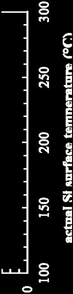
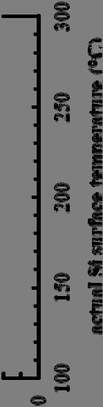
28 irtse: AL 2 O 3 ALD (PULSEWISE RESOLUTION) thickness increment per Al 2 O 3 ALD cycle (left) and pulsewise thickness changes (right) at varied deposition temperatures thickness inc crement per cycle (Å) 2 1 cummulative over 100 ALD cycles cyclewise by averaging last 10 of 100 ALD cycles actual Si surface temperature ( C) thicknes ss change (Å) thickness s change (Å) per TMA exposure actual Si surf. temp. ( C) 0-1 per O 3 exposure actual Si surf. temp. ( C) M. Junige et al.: 8 th Workshop Ellipsometry (AKE, Dresden, 2014).
29 IN-VACUO XPS: AL 2 O 3 ALD carbon XPS signal (in vacuo) at varied substrate set-point temperatures C 1s carbon contamination and Al-to-O ratio in dependence on the deposition temperature 50% 50:50 5 XPS in ntensity (a. u.) C 200 C 300 C 400 C 500 C ratio aluminum m-to-oxygen 40% 40:60 30% 30:70 20% 20:80 10% 10:90 0% (at.%) carbon cont tamination binding energy (ev) actual Si surface temperature ( C) V. Sharma: Student Research Project (Technische Universität Dresden, Dresden, 2014).
30 irtse: TAN X ALD (PULSEWISE RESOLUTION) averaged optical layer thickness in the course of one TaN x ALD cycle (left) and resp. details (right) at varied substrate set-point temperatures optical lay yer thickness s (Å) TBT TEMT NH time (s) 400 C 300 C 250 C 200 C 175 C 150 C 120 C thickness change (Å) thicknes ss change (Å) TBTEMT 3 8 time (s) () 13 NH time (s) M. Junige et al.: 12 th International Baltic ALD conference (Helsinki, 2014).


 at")

 thick")


 M.")


31 irtse: TAN X ALD (PULSEWISE RESOLUTION) thickness increment per TaN x ALD cycle (left) and pulsewise thickness changes (right) at varied deposition temperatures (Å) thick kness change thicknes ss change (Å) per TBTEMT exposure actual Si surf. temp. ( C) per NH 3 exposure actual Si surf. temp. ( C) M. Junige et al.: 12 th International Baltic ALD conference (Helsinki, 2014).


32 IN-VACUO XPS: TAN X ALD Nitrogen content Carbon and Oxygen concentration
33 Introduction of TU Dresden, Institute for Semiconductors and Microsystems and ALD applications TUD IHM) 1. Atomic Layer Deposition (ALD) basics 2. Tools and setups, parameters and complexity 3. Process development (Precursor qualification) - approaches (ex-situ, in-situ, in-situ 1 Cycle) -automated t testingti - advanced process development 4. Summary
34 Summary QCM and SE are capable to resolve sub monolayer effects This can be utilized to get information about the dynamics of the cycle The GPC combines the effect of two exposures and the dependency on process parameters need separately to be understood


35 Thank You! Spectroscopic Ellipsometer Quartz Crystal Microbalance X-ray / UV Photoelectron Spectroscope Scanning Probe Microscopep 4PP XRD Quadrupole Mass Spectrometer
Real-Time Chemical Sensing for Advanced Process Control in ALD
 Real-Time Chemical Sensing for Advanced Process Control in ALD Gary W. Rubloff 1, Laurent Henn-Lecordier 2, and Wei Lei 3 University of Maryland 1 Director, Maryland Center for Integrated Nano Science
Detection of Water in Low-k
 Fakultät Elektrotechnik und Informationstechnik, Institut für Halbleiter- und Mikrosystemtechnik Smart Failure Analysis for New Materials in Electronic Devices Detection of Water in Low-k Dielectric Films
Plasma Etching: Atomic Scale Surface Fidelity and 2D Materials
 1 Plasma Etching: Atomic Scale Surface Fidelity and 2D Materials Thorsten Lill, Keren J. Kanarik, Samantha Tan, Meihua Shen, Alex Yoon, Eric Hudson, Yang Pan, Jeffrey Marks, Vahid Vahedi, Richard A. Gottscho
In situ Studies of ALD Processes & Reaction Mechanisms
 In situ Studies of ALD Processes & Reaction Mechanisms Erwin Kessels w.m.m.kessels@tue.nl www.tue.nl/pmp This tutorial presentation will give (1) an overview of methods for in situ studies of ALD processes
In-situ Monitoring of Thin-Film Formation Processes by Spectroscopic Ellipsometry
 In-situ Monitoring of Thin-Film Formation Processes by Spectroscopic Ellipsometry Alexey Kovalgin Chair of Semiconductor Components MESA+ Institute for Nanotechnology Motivation Advantages of in-situ over
Atomic layer deposition of titanium nitride
 Atomic layer deposition of titanium nitride Jue Yue,version4, 04/26/2015 Introduction Titanium nitride is a hard and metallic material which has found many applications, e.g.as a wear resistant coating[1],
Hotwire-assisted Atomic Layer Deposition of Pure Metals and Metal Nitrides
 Hotwire-assisted Atomic Layer Deposition of Pure Metals and Metal Nitrides Alexey Kovalgin MESA+ Institute for Nanotechnology Semiconductor Components group a.y.kovalgin@utwente.nl 1 Motivation 1. Materials
Dynamic Equipment and Process Simulation for Atomic Layer Deposition Technology
 Dynamic Equipment and Process Simulation for Atomic Layer Deposition Technology Wei Lei, Yuhong Cai, Laurent Henn-Lecordier and Gary W. Rubloff Department of Materials Science and Engineering and Institute
EE C245 ME C218 Introduction to MEMS Design Fall 2007
 EE C245 ME C218 Introduction to MEMS Design Fall 2007 Prof. Clark T.-C. Nguyen Dept. of Electrical Engineering & Computer Sciences University of California at Berkeley Berkeley, CA 94720 Lecture 5: ALD,
Reaction Mechanism of Area-Selective Atomic
 Supporting Information Reaction Mechanism of Area-Selective Atomic Layer Deposition for Al 2 O 3 Nanopatterns Seunggi Seo 1, Il-Kwon Oh 1, Byung Chul Yeo 1, 2, Sang Soo Han 2, Chang Mo Yoon 1, JOON YOUNG
Step Coverage by ALD Films: Theory and Examples
 Step Coverage by ALD Films: Theory and Examples of Ideal and Non-Ideal Reactions Roy G. Gordon Cambridge, MA 1 L Step Coverage in Holes with High Aspect Ratio Step coverage = (b/a) x 100% a Aspect ratio
Low temperature atomic layer deposition of cobalt oxide as an effective catalyst for photoelectrochemical water splitting devices
 Low temperature atomic layer deposition of cobalt oxide as an effective catalyst for photoelectrochemical water splitting devices Jiyeon Kim, a Tomi Iivonen, b Jani Hämäläinen, b Marianna Kemell, b Kristoffer
EE C245 ME C218 Introduction to MEMS Design Fall 2007
 EE C245 ME C218 Introduction to MEMS Design Fall 2007 Prof. Clark T.-C. Nguyen Dept. of Electrical Engineering & Computer Sciences University of California at Berkeley Berkeley, CA 94720 Lecture 4: Film
Alternative deposition solution for cost reduction of TSV integration
 Alternative deposition solution for cost reduction of TSV integration J. Vitiello, F. Piallat, L. Bonnet KOBUS 611 rue Aristide Bergès, Z.A. de Pré Millet, Montbonnot-Saint-Martin, 38330 France Ph: +33
Technology for Micro- and Nanostructures Micro- and Nanotechnology
 Lecture 10: Deposition Technology for Micro- and Nanostructures Micro- and Nanotechnology Peter Unger mailto: peter.unger @ uni-ulm.de Institute of Optoelectronics University of Ulm http://www.uni-ulm.de/opto
CuH-ZSM-5 as Hydrocarbon Trap under cold. start conditions
 CuH-ZSM-5 as Hydrocarbon Trap under cold start conditions M. Navlani-García a, B. Puértolas b, D. Lozano-Castelló a, *, D. Cazorla-Amorós a, M. V. Navarro b, T. García b a Instituto Universitario de Materiales,
Modern Methods in Heterogeneous Catalysis Research: Preparation of Model Systems by Physical Methods
 Modern Methods in Heterogeneous Catalysis Research: Preparation of Model Systems by Physical Methods Methods for catalyst preparation Methods discussed in this lecture Physical vapour deposition - PLD
PHYSICAL AND CHEMICAL PROPERTIES OF ATMOSPHERIC PRESSURE PLASMA POLYMER FILMS
 PHYSICAL AND CHEMICAL PROPERTIES OF ATMOSPHERIC PRESSURE PLASMA POLYMER FILMS O. Goossens, D. Vangeneugden, S. Paulussen and E. Dekempeneer VITO Flemish Institute for Technological Research, Boeretang
Supplementary Information
 Supplementary Information Supplementary Figure 1. fabrication. A schematic of the experimental setup used for graphene Supplementary Figure 2. Emission spectrum of the plasma: Negative peaks indicate an
Agenda. 1. Atomic Layer Deposition Technology
 Agenda 1. Atomic Layer Deposition Technology 2. What is ALD? Atomic Layer Deposition is invented in 1977 by T. Suntola et al. - New Deposition Method for Electro-Luminescent Display (ZnS:Mn Thin Films)
Supporting Data. The University of Texas at Dallas, 800 West Campbell Road, Richardson, Texas 75080, United
 Supporting Data MoS 2 Functionalization for Ultra-thin Atomic Layer Deposited Dielectrics Angelica Azcatl, 1 Stephen McDonnell, 1 Santosh KC, 1 Xing Peng, 1 Hong Dong, 1 Xiaoye Qin, 1 Rafik Addou, 1 Greg
The effect of the chamber wall on fluorocarbonassisted atomic layer etching of SiO 2 using cyclic Ar/C 4 F 8 plasma
 The effect of the chamber wall on fluorocarbonassisted atomic layer etching of SiO 2 using cyclic Ar/C 4 F 8 plasma Running title: The effect of the chamber wall on FC assisted atomic layer etching of
Quantum Technology: Supplying the Picks and Shovels
 Quantum Technology: Supplying the Picks and Shovels Dr John Burgoyne Quantum Control Engineering: Mathematical Solutions for Industry Open for Business Event 7 th August 2014, 12.30-17.00, Isaac Newton
Direct-Write Deposition Utilizing a Focused Electron Beam
 Direct-Write Deposition Utilizing a Focused Electron Beam M. Fischer, J. Gottsbachner, S. Müller, W. Brezna, and H.D. Wanzenboeck Institute of Solid State Electronics, Vienna University of Technology,
TiO2/sapphire Beam Splitter for High-order Harmonics
 Technical Communication TiO2/sapphire Beam Splitter for High-order Harmonics Y. Sanjo*1, M. Murata*1, Y. Tanaka*1, H. Kumagai*1, and M. Chigane*2 *1 Graduate School of Engineering,Osaka City University,
Spin-resolved photoelectron spectroscopy
 Spin-resolved photoelectron spectroscopy Application Notes Spin-resolved photoelectron spectroscopy experiments were performed in an experimental station consisting of an analysis and a preparation chamber.
Supporting Information
 Supporting Information Yao et al. 10.1073/pnas.1416368111 Fig. S1. In situ LEEM imaging of graphene growth via chemical vapor deposition (CVD) on Pt(111). The growth of graphene on Pt(111) via a CVD process
The design of an integrated XPS/Raman spectroscopy instrument for co-incident analysis
 The design of an integrated XPS/Raman spectroscopy instrument for co-incident analysis Tim Nunney The world leader in serving science 2 XPS Surface Analysis XPS +... UV Photoelectron Spectroscopy UPS He(I)
XPS/UPS and EFM. Brent Gila. XPS/UPS Ryan Davies EFM Andy Gerger
 XPS/UPS and EFM Brent Gila XPS/UPS Ryan Davies EFM Andy Gerger XPS/ESCA X-ray photoelectron spectroscopy (XPS) also called Electron Spectroscopy for Chemical Analysis (ESCA) is a chemical surface analysis
Site seectivity in the initial oxidation of the Si 111-7=7 surface
 Applied Surface Science 126 1998 317 322 ž / Site seectivity in the initial oxidation of the Si 111-7=7 surface Jeong Sook Ha a,), Kang-Ho Park a, El-Hang Lee a, Seong-Ju Park b a Research Department,
The Benefit of Wide Energy Range Spectrum Acquisition During Sputter Depth Profile Measurements
 The Benefit of Wide Energy Range Spectrum Acquisition During Sputter Depth Profile Measurements Uwe Scheithauer, 82008 Unterhaching, Germany E-Mail: scht.uhg@googlemail.com Internet: orcid.org/0000-0002-4776-0678;
ALD & ALE Tutorial Speakers and Schedule
 ALD & ALE Tutorial Speakers and Schedule Sunday, July 29, 2018 1:00-1:05 Tutorial Welcome 1:05-1:50 1:50-2:35 2:35-3:20 Challenges of ALD Applications in Memory Semiconductor Devices, Choon Hwan Kim (SK
Process sensing and metrology in gate oxide growth by rapid thermal chemical vapor deposition from SiH 4 and N 2 O
 Process sensing and metrology in gate oxide growth by rapid thermal chemical vapor deposition from SiH 4 and N 2 O Guangquan Lu, a) Laura L. Tedder, b) and Gary W. Rubloff c) NSF Engineering Research Center
In-situ Ar Plasma Cleaning of Samples Prior to Surface Analysis
 In-situ Ar Plasma Cleaning of Samples Prior to Surface Analysis GE Global Research Vincent S. Smentkowski, Cameron Moore and Hong Piao 04GRC955, October 04 Public (Class ) Technical Information Series
Case Study of Electronic Materials Packaging with Poor Metal Adhesion and the Process for Performing Root Cause Failure Analysis
 Case Study of Electronic Materials Packaging with Poor Metal Adhesion and the Process for Performing Root Cause Failure Analysis Dr. E. A. Leone BACKGRUND ne trend in the electronic packaging industry
CVD: General considerations.
 CVD: General considerations. PVD: Move material from bulk to thin film form. Limited primarily to metals or simple materials. Limited by thermal stability/vapor pressure considerations. Typically requires
Towards Graphene-based heterojunction devices for microelectronic applications
 Towards Graphene-based heterojunction devices for microelectronic applications IHP GmbH Leibniz (Innovations for High Performance Microelectronics) TU-Dresden/IHM (Institute of Semiconductors and Microsystems)
Déposition séléctive le rêve reviens
 Willkommen Welcome Bienvenue Déposition séléctive le rêve reviens Patrik Hoffmann Michael Reinke, Yury Kuzminykh Ivo Utke, Carlos Guerra-Nunez, Ali Dabirian, Xavier Multone, Tristan Bret, Estelle Halary-Wagner,
Supplementary Figure S1 Scheme and description of the experimental setup. UHV-EC experiment includes the sample preparation and STM measurement in
 Supplementary Figure S1 Scheme and description of the experimental setup. UHV-EC experiment includes the sample preparation and STM measurement in UHV environment and transfer of the sample to the EC cell
Supporting Information
 Electronic Supplementary Material (ESI) for Journal of Materials Chemistry A. This journal is The Royal Society of Chemistry 2014 Supporting Information Sustainable photocatalytic production of hydrogen
Film Deposition Part 1
 1 Film Deposition Part 1 Chapter 11 : Semiconductor Manufacturing Technology by M. Quirk & J. Serda Spring Semester 2013 Saroj Kumar Patra Semidonductor Manufacturing Technology, Norwegian University of
Effects of plasma treatment on the precipitation of fluorine-doped silicon oxide
 ARTICLE IN PRESS Journal of Physics and Chemistry of Solids 69 (2008) 555 560 www.elsevier.com/locate/jpcs Effects of plasma treatment on the precipitation of fluorine-doped silicon oxide Jun Wu a,, Ying-Lang
Sensors and Metrology. Outline
 Sensors and Metrology A Survey 1 Outline General Issues & the SIA Roadmap Post-Process Sensing (SEM/AFM, placement) In-Process (or potential in-process) Sensors temperature (pyrometry, thermocouples, acoustic
Defense Technical Information Center Compilation Part Notice
 UNCLASSIFIED Defense Technical Information Center Compilation Part Notice ADP012830 TITLE: XPS Study of Cu-Clusters and Atoms in Cu/SiO2 Composite Films DISTRIBUTION: Approved for public release, distribution
Ellipsometric spectroscopy studies of compaction and decompaction of Si-SiO 2 systems
 Ellipsometric spectroscopy studies of compaction and decompaction of Si-SiO 2 systems Paper Witold Rzodkiewicz and Andrzej Panas Abstract The influence of the strain on the optical properties of Si-SiO
Graphene films on silicon carbide (SiC) wafers supplied by Nitride Crystals, Inc.
 wafers supplied by Nitride Crystals, Inc.") 9702 Gayton Road, Suite 320, Richmond, VA 23238, USA Phone: +1 (804) 709-6696 info@nitride-crystals.com www.nitride-crystals.com Graphene films on silicon carbide (SiC) wafers supplied by Nitride Crystals,
9702 Gayton Road, Suite 320, Richmond, VA 23238, USA Phone: +1 (804) 709-6696 info@nitride-crystals.com www.nitride-crystals.com Graphene films on silicon carbide (SiC) wafers supplied by Nitride Crystals,
Surface Functionalization by Atomic Layer Deposition
 Surface Functionalization by Atomic Layer Deposition Christophe Detavernier SIM User Forum - Gent 27/10/2015 CoCooN Conformal Coating of Nanomaterials Atomic layer deposition (ALD) Gas-phase thin film
Roll-to-roll equipment for atmospheric atomic layer deposition for solar applications
 Roll-to-roll equipment for atmospheric atomic layer deposition for solar applications Raymond Knaapen, VDL Enabling Technologies Group E-mail: Raymond.Knaapen@vdletg.com Amongst thin-film deposition techniques,
X-ray photoelectron spectroscopic characterization of molybdenum nitride thin films
 Korean J. Chem. Eng., 28(4), 1133-1138 (2011) DOI: 10.1007/s11814-011-0036-2 INVITED REVIEW PAPER X-ray photoelectron spectroscopic characterization of molybdenum nitride thin films Jeong-Gil Choi Department
Deuterium and fluorine radical reaction kinetics on photoresist*
 Deuterium and fluorine radical reaction kinetics on photoresist* Frank Greer, J. W. Coburn, and David B. Graves a) Department of Chemical Engineering, University of California, Berkeley, California 94720
Procédés de dépôt plasma avec injection pulsée de précurseurs (PECVD et PEALD) :
 :") Procédés de dépôt plasma avec injection pulsée de précurseurs (PECVD et PEALD) : Impact du réacteur et de la pression et développement de dépôts sélectifs C. Vallée 1,3, R. Gassilloud 2, R. Vallat 1,2,
Procédés de dépôt plasma avec injection pulsée de précurseurs (PECVD et PEALD) : Impact du réacteur et de la pression et développement de dépôts sélectifs C. Vallée 1,3, R. Gassilloud 2, R. Vallat 1,2,
Ceramic Processing Research
 Journal of Ceramic Processing Research. Vol. 11, No. 5, pp. 581~585 (2010) J O U R N A L O F Ceramic Processing Research The changing behavior of the dielectric constant of a-sic:h films deposited by remote
Hydrogenation of Single Walled Carbon Nanotubes
 Hydrogenation of Single Walled Carbon Nanotubes Anders Nilsson Stanford Synchrotron Radiation Laboratory (SSRL) and Stockholm University Coworkers and Ackowledgement A. Nikitin 1), H. Ogasawara 1), D.
Plasma Enhanced Chemical Vapor Deposition (PECVD) of Silicon Dioxide (SiO2) Using Oxford Instruments System 100 PECVD
 of Silicon Dioxide (SiO2) Using Oxford Instruments System 100 PECVD") University of Pennsylvania ScholarlyCommons Tool Data Browse by Type 2-7-2017 Plasma Enhanced Chemical Vapor Deposition (PECVD) of Silicon Dioxide (SiO2) Using Oxford Instruments System 100 PECVD Meredith
University of Pennsylvania ScholarlyCommons Tool Data Browse by Type 2-7-2017 Plasma Enhanced Chemical Vapor Deposition (PECVD) of Silicon Dioxide (SiO2) Using Oxford Instruments System 100 PECVD Meredith
Photoemission Spectroscopy
 FY13 Experimental Physics - Auger Electron Spectroscopy Photoemission Spectroscopy Supervisor: Per Morgen SDU, Institute of Physics Campusvej 55 DK - 5250 Odense S Ulrik Robenhagen,
DUV ( nm ) Characterization of Materials: A new instrument, the Purged UV Spectroscopic Ellipsometer,
 Characterization of Materials: A new instrument, the Purged UV Spectroscopic Ellipsometer,") WISE 2000, International Workshop on Spectroscopic Ellipsometry, 8 9 May 2000 DUV (150 350nm ) Characterization of Materials: A new instrument, the Purged UV Spectroscopic Ellipsometer, Pierre BOHER,,
WISE 2000, International Workshop on Spectroscopic Ellipsometry, 8 9 May 2000 DUV (150 350nm ) Characterization of Materials: A new instrument, the Purged UV Spectroscopic Ellipsometer, Pierre BOHER,,
Special Properties of Au Nanoparticles
 Special Properties of Au Nanoparticles Maryam Ebrahimi Chem 7500/750 March 28 th, 2007 1 Outline Introduction The importance of unexpected electronic, geometric, and chemical properties of nanoparticles
Evaluation of the plasmaless gaseous etching process
 Solid State Phenomena Vol. 134 (28) pp 7-1 Online available since 27/Nov/2 at www.scientific.net (28) Trans Tech Publications, Switzerland doi:1.428/www.scientific.net/ssp.134.7 Evaluation of the plasmaless
Plasma-assisted atomic layer deposition of Al2O3 studied by infrared transmission spectroscopy
 Eindhoven University of Technology MASTER Plasma-assisted atomic layer deposition of Al2O3 studied by infrared transmission spectroscopy Keijmel, J. Award date: 2008 Link to publication Disclaimer This
In-Situ FTIR Spectroscopy and Metrology of a Tungsten CVD Process
 In-Situ FTIR Spectroscopy and Metrology of a Tungsten CVD Process A. Singhal, L. Henn-Lecordier and J. N. Kidder Jr. University of Maryland, College Park, MD C.A. Gogol, J.F. Kushneir Inficon, Inc. East
Wet-chemical passivation of Si(111)- and Si(100)-substrates
- and Si(100)-substrates") Materials Science and Engineering B73 (2000) 178 183 www.elsevier.com/locate/mseb Wet-chemical passivation of Si(111)- and Si(100)-substrates H. Angermann a, *, W. Henrion a,a.röseler b, M. Rebien a a
Materials Science and Engineering B73 (2000) 178 183 www.elsevier.com/locate/mseb Wet-chemical passivation of Si(111)- and Si(100)-substrates H. Angermann a, *, W. Henrion a,a.röseler b, M. Rebien a a
X-Ray Photoelectron Spectroscopy (XPS) Prof. Paul K. Chu
 Prof. Paul K. Chu") X-Ray Photoelectron Spectroscopy (XPS) Prof. Paul K. Chu X-ray Photoelectron Spectroscopy Introduction Qualitative analysis Quantitative analysis Charging compensation Small area analysis and XPS imaging
X-Ray Photoelectron Spectroscopy (XPS) Prof. Paul K. Chu X-ray Photoelectron Spectroscopy Introduction Qualitative analysis Quantitative analysis Charging compensation Small area analysis and XPS imaging
Light-Induced Atom Desorption in Alkali Vapor Cells
 Fundamental Physics Using Atoms, 2010/08/09, Osaka Light-Induced Atom Desorption in Alkali Vapor Cells A. Hatakeyama (Tokyo Univ. Agr. Tech.) K. Hosumi K. Kitagami Alkali vapor cells UHV cell for laser
Wafer-scale fabrication of graphene
 Wafer-scale fabrication of graphene Sten Vollebregt, MSc Delft University of Technology, Delft Institute of Mircosystems and Nanotechnology Delft University of Technology Challenge the future Delft University
Reduced preferential sputtering of TiO 2 (and Ta 2 O 5 ) thin films through argon cluster ion bombardment.
 thin films through argon cluster ion bombardment.") NATIOMEM Reduced preferential sputtering of TiO 2 (and Ta 2 O 5 ) thin films through argon cluster ion bombardment. R. Grilli *, P. Mack, M.A. Baker * * University of Surrey, UK ThermoFisher Scientific
NATIOMEM Reduced preferential sputtering of TiO 2 (and Ta 2 O 5 ) thin films through argon cluster ion bombardment. R. Grilli *, P. Mack, M.A. Baker * * University of Surrey, UK ThermoFisher Scientific
PHI 5000 Versaprobe-II Focus X-ray Photo-electron Spectroscopy
 PHI 5000 Versaprobe-II Focus X-ray Photo-electron Spectroscopy The very basic theory of XPS XPS theroy Surface Analysis Ultra High Vacuum (UHV) XPS Theory XPS = X-ray Photo-electron Spectroscopy X-ray
Mass Spectrometry for Equipment, Process and Wafer State Sensing and Control
 Mass Spectrometry for Equipment, Process and Wafer State Sensing and Control Laura L. Tedder, G. Brian Lu and Gary W. Rubloff laura_tedder@ucsd.edu brian_lu@ncsu.edu gary_rubloff@ncsu.edu NSF Engineering
A DIVISION OF ULVAC-PHI
 A DIVISION OF ULVAC-PHI X-ray photoelectron spectroscopy (XPS/ESCA) is the most widely used surface analysis technique and has many well established industrial and research applications. XPS provides
Iodine-Mediated Chemical Vapor Deposition Growth of Metastable Transition Metal
 Supporting Information Iodine-Mediated Chemical Vapor Deposition Growth of Metastable Transition Metal Dichalcogenides Qiqi Zhang,, Yao Xiao, #, Tao Zhang,, Zheng Weng, Mengqi Zeng, Shuanglin Yue, ± Rafael
Atomic Layer Deposition of Hafnium Oxide at Temperatures below 100ºC. K. C. Kragh
 Atomic Layer Deposition of Hafnium Oxide at Temperatures below 100ºC K. C. Kragh Dept. of Physics and Optical Engineering, Rose-Hulman Institute of Technology REU Student in the Advanced Materials Research
Supplementary Materials
 Atomic layer-deposited tunnel oxide stabilizes silicon photoanodes for water oxidation Yi Wei Chen 1, Jonathan D. Prange 2, Simon Dühnen 2, Yohan Park 1, Marika Gunji 1, Christopher E. D. Chidsey 2, and
Processing and Characterization of GaSb/High-k Dielectric Interfaces. Pennsylvania 16802, USA. University Park, Pennsylvania 16802, USA
 10.1149/1.3630839 The Electrochemical Society Processing and Characterization of GaSb/High-k Dielectric Interfaces E. Hwang a, C. Eaton b, S. Mujumdar a, H. Madan a, A. Ali a, D. Bhatia b, S. Datta a and
nmos IC Design Report Module: EEE 112
 nmos IC Design Report Author: 1302509 Zhao Ruimin Module: EEE 112 Lecturer: Date: Dr.Zhao Ce Zhou June/5/2015 Abstract This lab intended to train the experimental skills of the layout designing of the
DEPOSITION OF THIN TiO 2 FILMS BY DC MAGNETRON SPUTTERING METHOD
 Chapter 4 DEPOSITION OF THIN TiO 2 FILMS BY DC MAGNETRON SPUTTERING METHOD 4.1 INTRODUCTION Sputter deposition process is another old technique being used in modern semiconductor industries. Sputtering
Evaluation of plasma strip induced substrate damage Keping Han 1, S. Luo 1, O. Escorcia 1, Carlo Waldfried 1 and Ivan Berry 1, a
 Solid State Phenomena Vols. 14-146 (29) pp 249-22 Online available since 29/Jan/6 at www.scientific.net (29) Trans Tech Publications, Switzerland doi:.428/www.scientific.net/ssp.14-146.249 Evaluation of
Hydrophilization of Fluoropolymers and Silicones
 2017 Adhesive and Sealant Council Spring Meeting Hydrophilization of Fluoropolymers and Silicones Aknowledgements: Wei Chen Mount Holyoke College NSF, NIH, Dreyfus, ACS-RF, MHC Bryony Coupe, Mamle Quarmyne,
Chemical Sensing and Sensor-based Metrology Using Mass Spectrometry in Multi-Component Reaction Systems
 Oct 25-29, 1999, AVS National Symposium, Seattle Chemical Sensing and Sensor-based Metrology Using Mass Spectrometry in Multi-Component Reaction Systems Y. Xu, T. Gougousi, N. Gupta, J. N. Kidder, Jr.,
Effect of Surface Contamination on Solid-State Bondability of Sn-Ag-Cu Bumps in Ambient Air
 Materials Transactions, Vol. 49, No. 7 (28) pp. 18 to 112 Special Issue on Lead-Free Soldering in Electronics IV #28 The Japan Institute of Metals Effect of Surface Contamination on Solid-State Bondability
Layer-modulated synthesis of uniform tungsten disulfide nanosheet using gas-phase precursors.
 Layer-modulated synthesis of uniform tungsten disulfide nanosheet using gas-phase precursors. Jusang Park * Hyungjun Kim School of Electrical and Electronics Engineering, Yonsei University, 262 Seongsanno,
Modeling of Ion Energy Distribution Using Time-Series Neural Network
 12th SEAS International Conference on SYSTEMS, Heralion, Greece, July 22-24, 2008 Modeling of Ion Energy Distribution Using Time-Series Neural Networ Suyeon Kim, Byungwhan Kim* Department of Electronic
arxiv: v1 [physics.plasm-ph] 30 May 2013
![arxiv: v1 [physics.plasm-ph] 30 May 2013](/thumbs/93/112809499.jpg "arxiv: v1 [physics.plasm-ph] 30 May 2013") arxiv:135.763v1 [physics.plasm-ph] 3 May 213 Time resolved measurement of film growth during reactive high power pulsed magnetron sputtering (HIPIMS) of titanium nitride F. Mitschker, M. Prenzel, J. Benedikt,
arxiv:135.763v1 [physics.plasm-ph] 3 May 213 Time resolved measurement of film growth during reactive high power pulsed magnetron sputtering (HIPIMS) of titanium nitride F. Mitschker, M. Prenzel, J. Benedikt,
Scanning Tunneling Microscopy and its Application
 Chunli Bai Scanning Tunneling Microscopy and its Application With 181 Figures SHANGHAI SCIENTIFIC & TECHNICAL PUBLISHERS Jpl Springer Contents 1. Introduction 1 1.1 Advantages of STM Compared with Other
Role of Electrochemical Reactions in the Degradation Mechanisms of AlGaN/GaN HEMTs
 Role of Electrochemical Reactions in the Degradation Mechanisms of AlGaN/GaN HEMTs Feng Gao 1,2, Bin Lu 2, Carl V. Thompson 1, Jesús del Alamo 2, Tomás Palacios 2 1. Department of Materials Science and
Resist-outgas testing and EUV optics contamination at NIST
 1 2012 International Workshop on EUVL, Maui, HI Resist-outgas testing and EUV optics contamination at NIST Shannon Hill, Nadir Faradzhev, Charles Tarrio, Steve Grantham, Lee Richter and Tom Lucatorto National
Insights into Interfacial Synergistic Catalysis over Catalyst toward Water-Gas Shift Reaction
 Supporting Information Insights into Interfacial Synergistic Catalysis over Ni@TiO2-x Catalyst toward Water-Gas Shift Reaction Ming Xu, 1 Siyu Yao, 2 Deming Rao, 1 Yiming Niu, 3 Ning Liu, 1 Mi Peng, 2
Surface Defects on Natural MoS 2
 Supporting Information: Surface Defects on Natural MoS 2 Rafik Addou 1*, Luigi Colombo 2, and Robert M. Wallace 1* 1 Department of Materials Science and Engineering, The University of Texas at Dallas,
Calculation of growth per cycle (GPC) of atomic layer deposited aluminium oxide nanolayers and dependence of GPC on surface OH concentration
 of atomic layer deposited aluminium oxide nanolayers and dependence of GPC on surface OH concentration") PRAMANA c Indian Academy of Sciences Vol. 82, No. 3 journal of March 2014 physics pp. 563 569 Calculation of growth per cycle (GPC) of atomic layer deposited aluminium oxide nanolayers and dependence of
PRAMANA c Indian Academy of Sciences Vol. 82, No. 3 journal of March 2014 physics pp. 563 569 Calculation of growth per cycle (GPC) of atomic layer deposited aluminium oxide nanolayers and dependence of
CVD-3 LFSIN SiN x Process
 CVD-3 LFSIN SiN x Process Top Electrode, C Bottom Electrode, C Pump to Base Time (s) SiH 4 Flow Standard LFSIN Process NH 3 Flow N 2 HF (watts) LF (watts) Pressure (mtorr Deposition Time min:s.s Pump to
Supplementary Information. Atomic Layer Deposition of Platinum Catalysts on Nanowire Surfaces for Photoelectrochemical Water Reduction
 Supplementary Information Atomic Layer Deposition of Platinum Catalysts on Nanowire Surfaces for Photoelectrochemical Water Reduction Neil P. Dasgupta 1 ǂ, Chong Liu 1,2 ǂ, Sean Andrews 1,2, Fritz B. Prinz
Energy Spectroscopy. Ex.: Fe/MgO
 Energy Spectroscopy Spectroscopy gives access to the electronic properties (and thus chemistry, magnetism,..) of the investigated system with thickness dependence Ex.: Fe/MgO Fe O Mg Control of the oxidation
Scanning Tunneling Microscopy Studies of the Ge(111) Surface
 Surface") VC Scanning Tunneling Microscopy Studies of the Ge(111) Surface Anna Rosen University of California, Berkeley Advisor: Dr. Shirley Chiang University of California, Davis August 24, 2007 Abstract: This
VC Scanning Tunneling Microscopy Studies of the Ge(111) Surface Anna Rosen University of California, Berkeley Advisor: Dr. Shirley Chiang University of California, Davis August 24, 2007 Abstract: This
Investigation of H 2 :CH 4 Plasma Composition by Means of Spatially Resolved Optical Spectroscopy
 Vol. 114 (2008) ACTA PHYSICA POLONICA A No. 6 A Optical and Acoustical Methods in Science and Technology Investigation of H 2 :CH 4 Plasma Composition by Means of Spatially Resolved Optical Spectroscopy
CVD-3 MFSIN-HU-1 SiN x Mixed Frequency Process
 CVD-3 MFSIN-HU-1 SiN x Mixed Frequency Process Standard MFSIN-HU-1 Process Top C Bottom C Pump to Base Time (s) SiH 4 Flow HF/ LF NH 3 Flow HF/LF N 2 HF/LF HF (watts) LF (watts) HF Time LF Time Pressure
Harvesting Heat through Seebeck Spin Tunneling Effect
 Harvesting Heat through Seebeck Spin Tunneling Effect Costel Constantin James Madison University Science Enabled by Photon Source, May 2012 Outline 1. Spintronics vs. Spin Caloritronics. 2. Novel Spin
Experimental 2.1 Introduction. Ultra high vacuum.
 2 Experimental 2.1 Introduction. Ultra high vacuum. The interest in solid-gas (or solid-vacuum) interfaces has been increasing rapidly during the last three decades. On one hand this is due to the practical
Solid State Science and Technology, Vol. 13, No 1 & 2 (2005) ISSN
 ISSN") FABRICATION OF Bi-Ti-O THIN FILM PRESSURE SENSOR PREPARED BY ELECTRON BEAM EVAPORATION METHOD Chong Cheong Wei, Muhammad Yahaya and Muhamad Mat Salleh Institue of Microengineering and Nanoelectronics,
FABRICATION OF Bi-Ti-O THIN FILM PRESSURE SENSOR PREPARED BY ELECTRON BEAM EVAPORATION METHOD Chong Cheong Wei, Muhammad Yahaya and Muhamad Mat Salleh Institue of Microengineering and Nanoelectronics,
Instrumentation and Operation
 Instrumentation and Operation 1 STM Instrumentation COMPONENTS sharp metal tip scanning system and control electronics feedback electronics (keeps tunneling current constant) image processing system data
Step-induced electronic resonance at vicinal Si(001) observed by spectroscopic SHG and RAS
 observed by spectroscopic SHG and RAS") Step-induced electronic resonance at vicinal Si(001) observed by spectroscopic SHG and RAS Robert Ehlert, Jinhee Kwon and Michael C. Downer Department of Physics, The University of Texas at Austin, Austin
Step-induced electronic resonance at vicinal Si(001) observed by spectroscopic SHG and RAS Robert Ehlert, Jinhee Kwon and Michael C. Downer Department of Physics, The University of Texas at Austin, Austin
A flexible research reactor for atomic layer deposition with a sample-transport chamber for in Vacuo analytics
 American Journal of Nano Research and Application 2014; 2(6-1): 34-38 Published online December 19, 2014 (http://www.sciencepublishinggroup.com/j/nano) doi: 10.11648/j.nano.s.2014020601.15 A flexible research
Subnanometre platinum clusters as highly active and selective catalysts for the oxidative dehydrogenation of propane
 DOI: 10.1038/NMAT2384 Subnanometre platinum clusters as highly active and selective catalysts for the oxidative dehydrogenation of propane Stefan Vajda, Larry A. Curtiss, Peter Zapol et al. Center for