Extended short wavelength infrared nbn photodetectors based on type II InAs/AlSb/GaSb superlattices with an AlAsSb/GaSb superlattice barrier
|
|
|
- MargaretMargaret Leonard
- 5 years ago
- Views:
Transcription
1 Extended short wavelength infrared nbn photodetectors based on type II InAs/AlSb/GaSb superlattices with an AlAsSb/GaSb superlattice barrier A. Haddadi, R. Chevallier, A. Dehzangi, and M. Razeghi 1,a) 1 Center for Quantum Devices, Department of Electrical Engineering and Computer Science, Northwestern University, Evanston, Illinois, 60208, USA Abstract Extended short wavelength infrared nbn photodetectors based on type II InAs/AlSb/GaSb superlattices on GaSb substrate have been demonstrated. An AlAs 0.10 Sb 0.90 /GaSb H structure superlattice design was used as the large bandgap electron barrier in these photodetectors. The photodetector is designed to have a 100% cut off wavelength of ~2.8 μm at 300K. The photodetector exhibited a room temperature (300 K) peak responsivity of 0.65 A/W at 1.9 μm, corresponding to a quantum efficiency of 41% at zero bias under front side illumination, without any anti reflection coating. With an R A of 78 Ω cm 2 and a dark current density of A/cm 2 under -400mV applied bias at 300 K, the nbn photodetector exhibited a specific detectivity of cm Hz 1/2 /W. At 150 K, the photodetector exhibited a dark current density of A/cm 2 and a quantum efficiency of 50%, resulting in a detectivity of cm Hz 1/2 /W. a) Corresponding author: razeghi@eecs.northwestern.edu 1
2 The extended short wavelength infrared (eswir) spectral range from 1.7 to 2.5 μm has many applications, including astronomy, earth sciences, and advanced optical communications. A camera that is capable of eswir imaging will produce a higher quality image than conventional short wavelength infrared (SWIR) cameras because roughly half of the available SWIR emission from the night sky falls between 1.7 to 2.5 μm. Up to now, a variety of material systems have addressed parts of this region; each of those material systems has its own advantages and disadvantages. For example, photodetectors based on In x Ga 1-x As compounds have shown high performance when nearly lattice matched to InP ( 1.7 μm cut off wavelength), but their performance reduces rapidly at longer wavelength due to mismatch induced defects. 1 Similarly, photodetectors based on mercury cadmium telluride (MCT) can cover the eswir spectral range; however, they require relatively complex material growth and device fabrication processes that significantly increase the production costs. In contrast, type II superlattices (T2SLs) are a developing material system that has recently demonstrated eswir spectral region coverage. 2,3 This material system has many intrinsic advantages such as low growth and manufacturing costs, great flexibility in bandgap engineering, the possibility for auger recombination suppression 4, and excellent material uniformity over large areas 5 which make it an attractive choice for infrared detection and imaging over the whole infrared spectrum. 6 However, while initial simple p i n homojunction eswir photodiodes based on T2SLs have been demonstrated, 2,3 the dark current density and specific detectivity of these photodetectors do not yet provide the ultra low noise that the T2SLs material system offers. Generation recombination (GR) is the dominant mechanism of dark 2
3 current generation in these p i n homojunction eswir photodetectors when operating at low temperatures (< 250 K). 2,3 However, performance can be dramatically improved by adopting a heterojunction based photodetector structure, such as nbn 7, which can significantly reduce the GR based dark current and, ultimately, total dark current density of the device. In this letter, we present the demonstration of eswir nbn photodetectors based on InAs/AlSb/GaSb type II superlattices with wide bandgap AlAs 0.10 Sb 0.90 /GaSb superlattice based electron barriers. The AlAs 0.10 Sb 0.90 layer in the AlAsSb/GaSb superlattices is lattice matched to GaSb substrate and has antimony (Sb) atom in common with GaSb that provides a great deal of flexibility in the superlattice design, and unlike M 8 and W superlattices 9 it does not require any special interface design or strain balancing. Because of the common anion rule of band lineups, the valence band offset between AlAs 0.10 Sb 0.90 and GaSb is small; thus, it provides little possibility to engineer the valence band. However, the electron quantum well in this superlattice is deep ( 1.19 ev 13,14 ) and thus this superlattice can be tuned to make the wide bandgap electron barriers necessary for eswir nbn photodetectors. Furthermore, using an AlAs 0.10 Sb 0.90 /GaSb superlattice as the electron barrier results in a smoother surface morphology compared to the case in which the barrier consists of a simple ternary AlAs 0.10 Sb 0.90 layer. The growth conditions for AlAs 0.10 Sb 0.90 /GaSb superlattices are exactly the same as for InAs/AlSb/GaSb T2SL and the heterostructure can be experimentally realized without any difficulty, such as an increase in strain or interface problems. All of these makes AlAs 0.10 Sb 0.90 /GaSb superlattices an ideal wide bandgap addition to the 6.1 Å family of materials. We call 3
4 this design an H structure superlattice because of the deep wells, as shown in the inset of Figure 1. With those advantages, the H structure superlattice was inserted as the electron barrier between an n contact layer and an n type eswir absorption region to create a nbn photodetector for this study. The eswir absorption region and n contact were chosen to have 8/1/5/1 mono layers (MLs) of InAs/GaSb/AlSb/GaSb and 5/1/5/1 MLs of InAs/GaSb/AlSb/GaSb, respectively. It was expected that absorption region and n contact would have cut off wavelengths of ~2.5 and ~1.9 μm, respectively, at 150 K. The electron barrier H structure superlattice is 300 nm thick consisting of 5/2 MLs of AlAs 0.10 Sb 0.90 /GaSb, respectively, with a bandgap energy of ~1 ev (equal to a 1 μm cut off wavelength) at 150 K. The H structure superlattices barrier needs to be thick enough so that there is a negligible electron tunneling through it and the barrier should be high enough so there is a negligible thermal excitation of majority carriers over it and a negligible absorption inside the electron barrier near the cut off of the photodetector. The heterojunction between the electron barrier and the eswir absorption layer should have a large energy discontinuity in the conduction band and near zero energy discontinuity in the valence band. From the empirical tight binding model (ETBM) calculations, the band discontinuity between the barrier and absorption region is 20 mev in the valence band and 546 mev in the conduction band. The presence of this wide bandgap barrier not only reduces the GR based dark current but also reduces the trap assisted and band to band tunneling. The complete photodetector structure is shown in Figure 1. 4
5 Figure 1. Schematic diagram the eswir nbn photodetector with the inset showing the superlattice band alignment of the H structure electron barrier. The colored rectangles in the inset represent the forbidden gap of component materials. The dashed lines represent the effective conduction and valence bands of the H structure superlattice. After selecting the proper superlattice design for each part of the photodetector structure (see Figure 1), the device was grown using a solid source molecular beam epitaxy (SSMBE) reactor equipped with group III SUMO cells and group V valved crackers. The material was grown on a Te doped n type (10 17 cm -3 ) GaSb wafer. The epitaxial growth of the photodetector was started by growing a 100 nm thick GaSb buffer layer to smooth out the surface, then, a 500 nm n doped InAs 0.91 Sb 0.09 buffer layer (10 18 cm -3 ), followed by a 500 nm thick n type eswir contact (10 18 cm -3 ), a 1 μm thick n type eswir absorption region (10 14 cm -3 ), a 300 nm thick electron barrier, and a 200 nm thick SWIR n contact (10 18 cm -3 ). Unlike the eswir bottom n contact which shares the same superlattice design with the absorption region, the top SWIR n contact superlattice design has larger bandgap energy to eliminate absorption by the top n 5
6 contact near the spectral cut off of the photodetector in front side illumination configuration. Silicon (Si) was used as the n type dopant. Figure 2. (a) The atomic force microscopy image of a m 2 surface area of the grown material, for the nbn device with RMS roughness value of 1.21 Å. (b) High-resolution X-ray diffraction (HR- XRD) of the material grown for the nbn device. The quality of the material was assessed after epitaxial growth using atomic force microscopy (AFM) and high resolution X ray diffraction (HR XRD). The sample exhibits good surface morphology with clear atomic steps and a small surface roughness of 1.21 Å over a μm 2 area which indicates no structural degradation is created by the addition of the H structure superlattice barrier (Figure 2-a). 2,3 The satellite peaks in the HR XRD scan showed the overall periods of the eswir absorption region, the electron barrier, and the top SWIR n contact were about 52, 22, and 43 Å, respectively. The lattice mismatch to the GaSb substrate of the three superlattices was less than 1500 ppm, which is in agreement with the superlattice design (Figure 2-b). After structural characterization, the wafer was processed into a set of unpassivated mesa isolated nbn photodetectors with device areas ranging from to cm 2 using standard photo lithographic processing techniques. 15 The photodetectors were left unpassivated but in order to minimize the surface leakage special 6
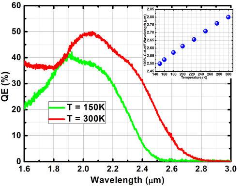
7 attention was paid to ensure the surface were kept clean and minimal surface oxidization occurred. Then, the sample was wire bonded to a 68 pin leadless ceramic chip carrier (LCCC). Finally, it was loaded into a cryostat for both optical and electrical characterization at temperatures ranging from 150 to 300 K. Figure 3. Saturated 150 and 300 K quantum efficiency spectra of the nbn photodetector in front-side illumination configuration without any anti-reflection coating. Inset: The variation of the 100% cut-off wavelength of the device vs. temperature. The nbn photodetectors were front side illuminated using either calibrated 1000 C blackbody source or a Bruker IFS 66v/S Fourier transform infrared (FTIR) spectrometer. No anti reflection (AR) coating was applied to the nbn photodetectors. The optical performance of the devices is shown in Figure 3. The photodetectors exhibit a 100% cut off wavelength of ~2.5 m at 150 K (Figure 3 inset) as predicted from the band structure calculations; the device responsivity then peaks at 0.65 A/W, corresponding to quantum 7

 Dark current density vs.")
8 efficiency (QE) of 41% for a 1 μm thick absorption region. At 300 K, the sample shows a 100% cut off wavelength at ~2.8 m; the device responsivity then peaks at 0.82 A/W, corresponding to a quantum efficiency of 50%. The device QE spectrum reaches to its saturation point under -400 mv applied bias voltage. The decreased quantum efficiency at shorter wavelengths is caused by partial absorption of the short wavelength light in the top SWIR n contact where it does not contribute to the photo current of the device. This issue can be addressed by thinner top contacts or larger bandgap energies. Figure 4. (a) Dark current density vs. applied bias voltage characteristic of the photodetectors as a function of temperature. (b) Arrhenius plot of the dark current density of the photodetector under mv applied bias. The green and red lines represent the expected diffusion and generationrecombination (G-R) limits, respectively. Figure 4(a) presents the dark current density vs. applied bias voltage characteristics of the nbn photodetector at different temperatures ranging from 150 to 300 K. At 150 K, the 8
9 photodetector exhibits a dark current density of A/cm 2 under -400mV applied bias, whereas at room temperature (T = 300 K), the dark current density at -400mV is A/cm 2. In T2SL based homojunction photodiodes operating in the SWIR region, 2,3 the diffusion current at temperatures below 200 K is typically several orders of magnitude lower than the GR current, while at room temperature it is several orders higher. An Arrhenius plot of the dark current density versus inverse temperature (1/T) from 150 to 300 K under -400 mv applied bias voltage is shown in Figure 4(b). The dark current of this nbn photodetector is diffusion limited at operating temperatures above 180 K, and G R current limited below this temperature, with both G R and diffusion current being equal at 180 K (the cross over temperature, T 0 ). In contrast, the cross over temperature of our previous T2SL based homojunction SWIR photodiodes 2,3 was very close to or higher than room temperature. The nbn device architecture has enabled us to push T 0 to significantly lower operating temperatures which leads to lower dark current than that of homojunction T2SL based photodiode operating at the same temperature. Alternately, this device can operate at a higher temperature with the same dark current. In addition to the intrinsic improvement of the electrical performance, the nbn photodetector design also lends itself well to a shallow etched device geometry. The mesa etch can terminates at the wide bandgap H structure superlattice barrier and the smaller bandgap eswir absorption region does not need to be etched, thus avoiding surface leakage. This can lead to more uniform in focal plane arrays. Figure 4(b) also suggests that there is still room for further improvement of the low temperature (< 180 K) electrical performance by further suppressing G R current. 9
10 Figure 5. Specific detectivity (D * ) spectrum of the device at (a) 150 K and (b) 300 K. at -400 mv applied bias. The device is front-side illuminated, without any anti-reflection coating. The specific detectivity is calculated based on the equation in the inset, where R i is the device responsivity, J is the dark current density, R A is the differential resistance area product, k b is the Boltzmann constant, and T is the operating temperature. After performing both electrical and optical characterization of the nbn photodetector, the specific detectivity (D * ) was calculated. The device exhibits a saturated dark current shot noise limited specific detectivity of cm Hz 1/2 /W under -400 mv of applied bias at 150 K (Figure 5 a). At 300 K, the photodetector exhibits a specific detectivity of cm Hz 1/2 /W under -400 mv applied bias (Figure 5 b) for the same background condition. In summary, we have reported the design, growth, and characterization of high performance eswir nbn photodetectors based on InAs/AlSb/GaSb type II superlattices. An AlAs 0.10 Sb 0.90 /GaSb wide-bandgap H structure superlattice design was used as the 10
11 electron barrier. These nbn photodetectors exhibit 100% cut off wavelengths of ~2.5 and ~2.8 m at 150 and 300 K, respectively. The devices achieve saturated quantum efficiency values of 41% and 50% at 150 and 300 K, respectively, under front side illumination and without any AR coating. At 150 K, the photodetectors exhibit a dark current density of A/cm 2 under 400 mv applied bias providing a specific detectivity of cm Hz 1/2 /W. At 300 K, the dark current density reaches A/cm 2 under -400 mv bias, providing a specific detectivity of cm Hz 1/2 /W. The H structure superlattice based electron barrier design in combination with nbn photodetector architecture has made it possible for T2SL based eswir to operate with lower dark current densities. Moreover, using digital readout integrated circuits (digital ROIC) that have unlimited charge integration capability this photodetector could be used for high performance room temperature imaging. This will open the possibility of incorporating T2SL based eswir photodetectors in high performance infrared imaging systems and makes type II superlattices a viable candidate for making high performance infrared imagers and a possible replacement for current state of the art technologies. This material is based on research sponsored by Air Force Research Laboratory (AFRL) under agreement number FA
12 References L. O. Bubulac, W. E. Tennant, J. G. Pasko, L. J. Kozlowski, M. Zandian, M. E. Motamedi, R. E. De Wames, J. Bajaj, N. Nayar, W. V. McLevige, N. S. Gluck, R. Melendes, D. E. Cooper, D. D. Edwall, J. M. Arias, R. Hall, and A. I. D souza, Journal of Electronic Materials 26, 649 (1997). A. M. Hoang, G. Chen, A. Haddadi, S. A. Pour, and M. Razeghi, Applied Physics Letters 100, (2012). A. Haddadi, X. V. Suo, S. Adhikary, P. Dianat, R. Chevallier, A. M. Hoang, and M. Razeghi, Applied Physics Letters 107, (2015). G. G. Zegrya and A. D. Andreev, Applied Physics Letters 67, 2681 (1995). N. Binh-Minh, C. Guanxi, H. Minh-Anh, and M. Razeghi, Quantum Electronics, IEEE Journal of 47, 686 (2011). M. Razeghi, in US Patent (2005). S. Maimon and G. W. Wicks, Applied Physics Letters 89, (2006). B.-M. Nguyen, D. Hoffman, P.-Y. Delaunay, and M. Razeghi, Applied Physics Letters 91, (2007). C. S. Kim, C. L. Canedy, E. H. Aifer, M. Kim, W. W. Bewley, J. G. Tischler, D. C. Larrabee, J. A. Nolde, J. H. Warner, I. Vurgaftman, E. M. Jackson, and J. R. Meyer, Journal of Vacuum Science & Technology B: Microelectronics and Nanometer Structures Processing, Measurement, and Phenomena 25, 991 (2007). J. O. McCaldin, T. C. McGill, and C. A. Mead, Physical Review Letters 36, 56 (1976). W. R. Frensley and H. Kroemer, Physical Review B 16, 2642 (1977). W. A. Harrison, Journal of Vacuum Science and Technology 14, 1016 (1977). I. Vurgaftman, J. R. Meyer, and L. R. Ram-Mohan, Journal of Applied Physics 89, 5815 (2001). G. Griffiths, K. Mohammed, S. Subbana, H. Kroemer, and J. L. Merz, Applied Physics Letters 43, 1059 (1983). A. Hood, D. Hoffman, B.-M. Nguyen, P.-Y. Delaunay, E. Michel, and M. Razeghi, Applied Physics Letters 89, (2006). 12

13

14
15

16

17
Very long wavelength type-ii InAs/GaSb superlattice infrared detectors
 Very long wavelength type-ii InAs/GaSb superlattice infrared detectors L. Höglund 1, J. B. Rodriguez 2, S. Naureen 1, R. Ivanov 1, C. Asplund 1, R. Marcks von Würtemberg 1, R. Rossignol 2, P. Christol
Chapter 3 The InAs-Based nbn Photodetector and Dark Current
 68 Chapter 3 The InAs-Based nbn Photodetector and Dark Current The InAs-based nbn photodetector, which possesses a design that suppresses surface leakage current, is compared with both a commercially available
Barrier Photodetectors for High Sensitivity and High Operating Temperature Infrared Sensors
 Barrier Photodetectors for High Sensitivity and High Operating Temperature Infrared Sensors Philip Klipstein General Review of Barrier Detectors 1) Higher operating temperature, T OP 2) Higher signal to
InAs/GaSb Mid-Wave Cascaded Superlattice Light Emitting Diodes
 InAs/GaSb Mid-Wave Cascaded Superlattice Light Emitting Diodes John Prineas Department of Physics and Astronomy, University of Iowa May 3, 206 Collaborator: Thomas Boggess Grad Students: Yigit Aytak Cassandra
Growth and characteristics of type-ii InAs/GaSb superlattice-based detectors
 Growth and characteristics of type-ii InAs/GaSb superlattice-based detectors A. Khoshakhlagh*, D. Z. Ting, A. Soibel, L. Höglund, J. Nguyen, S. A. Keo, A. Liao, and S. D. Gunapala Jet Propulsion Laboratory,
PIN versus PN Homojunctions in GaInAsSb Micron Mesa Photodiodes
 PIN versus PN Homojunctions in GaInAsSb 2.0-2.5 Micron Mesa Photodiodes J. P. Prineas a,b, J.R. Yager a,b, J. T. Olesberg b,c, S. Seydmohamadi a,b, C. Cao a,b, M. Reddy b, C. Coretsopoulos b, J. L. Hicks
XBn and XBp infrared detectors
 XBn and XBp infrared detectors P.C. Klipstein, SemiConductor Devices P.O. Box 22, Haifa 31021, Israel XBn and XBp barrier detectors grown from III-V materials on GaSb substrates have recently been shown
DESIGN AND FABRICATION OF HIGH- PERFORMANCE LWIR PHOTODETECTORS BASED ON TYPE-II SUPERLATTICES
 AFRL-RV-PS- TR-2017-0090 AFRL-RV-PS- TR-2017-0090 DESIGN AND FABRICATION OF HIGH- PERFORMANCE LWIR PHOTODETECTORS BASED ON TYPE-II SUPERLATTICES Manijeh Razeghi Northwestern University 2220 Campus Dr.,
Lecture 3: Heterostructures, Quasielectric Fields, and Quantum Structures
 Lecture 3: Heterostructures, Quasielectric Fields, and Quantum Structures MSE 6001, Semiconductor Materials Lectures Fall 2006 3 Semiconductor Heterostructures A semiconductor crystal made out of more
OPTI510R: Photonics. Khanh Kieu College of Optical Sciences, University of Arizona Meinel building R.626
 OPTI510R: Photonics Khanh Kieu College of Optical Sciences, University of Arizona kkieu@optics.arizona.edu Meinel building R.626 Announcements Homework #6 is assigned, due May 1 st Final exam May 8, 10:30-12:30pm
Chapter 5 Lateral Diffusion Lengths of Minority Carriers
 111 Chapter 5 Lateral Diffusion Lengths of Minority Carriers The nbn photodetector is proposed as a tool for measuring the lateral diffusion length of minority carriers in an epitaxially grown crystal
InGaAs-AlAsSb quantum cascade lasers
 InGaAs-AlAsSb quantum cascade lasers D.G.Revin, L.R.Wilson, E.A.Zibik, R.P.Green, J.W.Cockburn Department of Physics and Astronomy, University of Sheffield, UK M.J.Steer, R.J.Airey EPSRC National Centre
Electron Energy, E E = 0. Free electron. 3s Band 2p Band Overlapping energy bands. 3p 3s 2p 2s. 2s Band. Electrons. 1s ATOM SOLID.
 Electron Energy, E Free electron Vacuum level 3p 3s 2p 2s 2s Band 3s Band 2p Band Overlapping energy bands Electrons E = 0 1s ATOM 1s SOLID In a metal the various energy bands overlap to give a single
Design of InAs/Ga(In)Sb superlattices for infrared sensing
Sb superlattices for infrared sensing") Microelectronics Journal 36 (25) 256 259 www.elsevier.com/locate/mejo Design of InAs/Ga(In)Sb superlattices for infrared sensing G.J. Brown*, F. Szmulowicz, H. Haugan, K. Mahalingam, S. Houston Air Force
Microelectronics Journal 36 (25) 256 259 www.elsevier.com/locate/mejo Design of InAs/Ga(In)Sb superlattices for infrared sensing G.J. Brown*, F. Szmulowicz, H. Haugan, K. Mahalingam, S. Houston Air Force
Cross-Section Scanning Tunneling Microscopy of InAs/GaSb Superlattices
 Cross-Section Scanning Tunneling Microscopy of InAs/GaSb Superlattices Cecile Saguy A. Raanan, E. Alagem and R. Brener Solid State Institute. Technion, Israel Institute of Technology, Haifa 32000.Israel
Single Photon detectors
 Single Photon detectors Outline Motivation for single photon detection Semiconductor; general knowledge and important background Photon detectors: internal and external photoeffect Properties of semiconductor
DEVICE CHARACTERISTICS OF VLWIR MCT PHOTODIODES. August 1999
 Approved for public release; distribution is unlimited. DEVICE CHARACTERISTICS OF VLWIR MCT PHOTODIODES August 1999 R.E. DeWames, P.S. Wijewarnasuriya, W. McLevige, D. Edwall, G. Hildebrandt, and J.M.
Reticulated shallow etch mesa isolation (RSEMI) for controlling surface leakage in GaSb-based infrared detectors
 for controlling surface leakage in GaSb-based infrared detectors") Reticulated shallow etch mesa isolation (RSEMI) for controlling surface leakage in GaSb-based infrared detectors J. A. Nolde, 1,a) E. M. Jackson, 1 M. F. Bennett, 2 C. A. Affouda, 1 E. R. Cleveland, 1
Reticulated shallow etch mesa isolation (RSEMI) for controlling surface leakage in GaSb-based infrared detectors J. A. Nolde, 1,a) E. M. Jackson, 1 M. F. Bennett, 2 C. A. Affouda, 1 E. R. Cleveland, 1
Photonic Communications Engineering Lecture. Dr. Demetris Geddis Department of Engineering Norfolk State University
 Photonic Communications Engineering Lecture Dr. Demetris Geddis Department of Engineering Norfolk State University Light Detectors How does this detector work? Image from visionweb.com Responds to range
File name: Supplementary Information Description: Supplementary Figures and Supplementary References. File name: Peer Review File Description:
 File name: Supplementary Information Description: Supplementary Figures and Supplementary References File name: Peer Review File Description: Supplementary Figure Electron micrographs and ballistic transport
PHOTOVOLTAICS Fundamentals
 PHOTOVOLTAICS Fundamentals PV FUNDAMENTALS Semiconductor basics pn junction Solar cell operation Design of silicon solar cell SEMICONDUCTOR BASICS Allowed energy bands Valence and conduction band Fermi
Accepted Manuscript. Manufacturability of type-ii InAs/GaSb superlattice detectors for infrared imaging
 Accepted Manuscript Manufacturability of type-ii InAs/GaSb superlattice detectors for infrared imaging L. Höglund, C. Asplund, R. Marcks von Würtemberg, H. Kataria, A. Gamfeldt, S. Smuk, H. Martijn, E.
Practical 1P4 Energy Levels and Band Gaps
 Practical 1P4 Energy Levels and Band Gaps What you should learn from this practical Science This practical illustrates some of the points from the lecture course on Elementary Quantum Mechanics and Bonding
LEC E T C U T R U E R E 17 -Photodetectors
 LECTURE 17 -Photodetectors Topics to be covered Photodetectors PIN photodiode Avalanche Photodiode Photodetectors Principle of the p-n junction Photodiode A generic photodiode. Photodetectors Principle
Lecture 12. Semiconductor Detectors - Photodetectors
 Lecture 12 Semiconductor Detectors - Photodetectors Principle of the pn junction photodiode Absorption coefficient and photodiode materials Properties of semiconductor detectors The pin photodiodes Avalanche
Practical 1P4 Energy Levels and Band Gaps
 Practical 1P4 Energy Levels and Band Gaps What you should learn from this practical Science This practical illustrates some of the points from the lecture course on Elementary Quantum Mechanics and Bonding
Ge Quantum Well Modulators on Si. D. A. B. Miller, R. K. Schaevitz, J. E. Roth, Shen Ren, and Onur Fidaner
 10.1149/1.2986844 The Electrochemical Society Ge Quantum Well Modulators on Si D. A. B. Miller, R. K. Schaevitz, J. E. Roth, Shen Ren, and Onur Fidaner Ginzton Laboratory, 450 Via Palou, Stanford CA 94305-4088,
ANTIMONY ENHANCED HOMOGENEOUS NITROGEN INCORPORATION INTO GaInNAs FILMS GROWN BY ATOMIC HYDROGEN-ASSISTED MOLECULAR BEAM EPITAXY
 ANTIMONY ENHANCED HOMOGENEOUS NITROGEN INCORPORATION INTO GaInNAs FILMS GROWN BY ATOMIC HYDROGEN-ASSISTED MOLECULAR BEAM EPITAXY Naoya Miyashita 1, Nazmul Ahsan 1, and Yoshitaka Okada 1,2 1. Research Center
High-performance mid-infrared quantum dot infrared photodetectors
 INSTITUTE OF PHYSICS PUBLISHING JOURNAL OF PHYSICS D: APPLIED PHYSICS J. Phys. D: Appl. Phys. 38 (2005) 2135 2141 doi:10.1088/0022-3727/38/13/009 High-performance mid-infrared quantum dot infrared photodetectors
Transient Harman Measurement of the Cross-plane ZT of InGaAs/InGaAlAs Superlattices with Embedded ErAs Nanoparticles
 Transient Harman Measurement of the Cross-plane ZT of InGaAs/InGaAlAs Superlattices with Embedded ErAs Nanoparticles Rajeev Singh, Zhixi Bian, Gehong Zeng, Joshua Zide, James Christofferson, Hsu-Feng Chou,
Superconducting Ti/TiN thin films for mm wave absorption
 Superconducting /N thin films for mm wave absorption A.Aliane 1, M. Solana 2, V. Goudon 1, C. Vialle 1, S. Pocas 1, E. Baghe 1, L. Carle 1, W. Rabaud 1, L. Saminadayar 2, L. Dussopt 1, P.Agnese 1, N. Lio
Graphene photodetectors with ultra-broadband and high responsivity at room temperature
 SUPPLEMENTARY INFORMATION DOI: 10.1038/NNANO.2014.31 Graphene photodetectors with ultra-broadband and high responsivity at room temperature Chang-Hua Liu 1, You-Chia Chang 2, Ted Norris 1.2* and Zhaohui
GROWTH AND CHARACTERIZATION STUDIES OF ADVANCED INFRARED HETEROSTRUCTURES
 AFRL-RV-PS- TR-2015-0126 AFRL-RV-PS- TR-2015-0126 GROWTH AND CHARACTERIZATION STUDIES OF ADVANCED INFRARED HETEROSTRUCTURES Sanjay Krishna University of New Mexico 1313 Goddard SE Albuquerque, NM 87106
A normal-incident quantum well infrared photodetector enhanced by surface plasmon resonance
 Best Student Paper Award A normal-incident quantum well infrared photodetector enhanced by surface plasmon resonance Wei Wu a, Alireza Bonakdar, Ryan Gelfand, and Hooman Mohseni Bio-inspired Sensors and
Short wavelength and strain compensated InGaAs-AlAsSb. AlAsSb quantum cascade lasers. D.Revin, S.Zhang, J.Cockburn, L.Wilson, S.
 Short wavelength and strain compensated InGaAs-AlAsSb AlAsSb quantum cascade lasers D.Revin, S.Zhang, J.Cockburn, L.Wilson, S.Menzel, Department of Physics and Astronomy, University of Sheffield, United
Laser Diodes. Revised: 3/14/14 14: , Henry Zmuda Set 6a Laser Diodes 1
 Laser Diodes Revised: 3/14/14 14:03 2014, Henry Zmuda Set 6a Laser Diodes 1 Semiconductor Lasers The simplest laser of all. 2014, Henry Zmuda Set 6a Laser Diodes 2 Semiconductor Lasers 1. Homojunction
Chapter 1 Overview of Semiconductor Materials and Physics
 Chapter 1 Overview of Semiconductor Materials and Physics Professor Paul K. Chu Conductivity / Resistivity of Insulators, Semiconductors, and Conductors Semiconductor Elements Period II III IV V VI 2 B
Semiconductors. SEM and EDAX images of an integrated circuit. SEM EDAX: Si EDAX: Al. Institut für Werkstoffe der ElektrotechnikIWE
 SEM and EDAX images of an integrated circuit SEM EDAX: Si EDAX: Al source: [Cal 99 / 605] M&D-.PPT, slide: 1, 12.02.02 Classification semiconductors electronic semiconductors mixed conductors ionic conductors
Chapter 17. λ 2 = 1.24 = 6200 Å. λ 2 cutoff at too short a wavelength λ 1 cutoff at to long a wavelength (increases bandwidth for noise reduces S/N).
.") 70 Chapter 17 17.1 We wish to use a photodiode as a detector for a signal of 9000 Å wavelength. Which would be the best choice of material for the photodiode, a semiconductor of bandgap = 0.5 ev, bandgap
70 Chapter 17 17.1 We wish to use a photodiode as a detector for a signal of 9000 Å wavelength. Which would be the best choice of material for the photodiode, a semiconductor of bandgap = 0.5 ev, bandgap
Chapter 7. Solar Cell
 Chapter 7 Solar Cell 7.0 Introduction Solar cells are useful for both space and terrestrial application. Solar cells furnish the long duration power supply for satellites. It converts sunlight directly
February 1, 2011 The University of Toledo, Department of Physics and Astronomy SSARE, PVIC
 FUNDAMENTAL PROPERTIES OF SOLAR CELLS February 1, 2011 The University of Toledo, Department of Physics and Astronomy SSARE, PVIC Principles and Varieties of Solar Energy (PHYS 4400) and Fundamentals of
Novel materials and nanostructures for advanced optoelectronics
 Novel materials and nanostructures for advanced optoelectronics Q. Zhuang, P. Carrington, M. Hayne, A Krier Physics Department, Lancaster University, UK u Brief introduction to Outline Lancaster University
Sponsored by. Contract No. N K-0073: Modification P00006 DARPA Order 5674 NR
 OTIC FILE COP Study of Interfacial Chemistry between Metals and Their Effects on Electronic Systems q. o Sponsored by 00 Defense Advanced Research Projects Agency (DOD) and The Office of Naval Research
Piezoresistive effect in p-type 3C-SiC at high temperatures characterized using Joule heating
 Electronic Supplementary Information Piezoresistive effect in p-type 3C-SiC at high temperatures characterized using Joule heating Hoang-Phuong Phan, 1 Toan Dinh, 1 Takahiro Kozeki, 2 Afzaal Qamar, 1 Takahiro
LOW-TEMPERATURE Si (111) HOMOEPITAXY AND DOPING MEDIATED BY A MONOLAYER OF Pb
 HOMOEPITAXY AND DOPING MEDIATED BY A MONOLAYER OF Pb") LOW-TEMPERATURE Si (111) HOMOEPITAXY AND DOPING MEDIATED BY A MONOLAYER OF Pb O.D. DUBON, P.G. EVANS, J.F. CHERVINSKY, F. SPAEPEN, M.J. AZIZ, and J.A. GOLOVCHENKO Division of Engineering and Applied Sciences,
LOW-TEMPERATURE Si (111) HOMOEPITAXY AND DOPING MEDIATED BY A MONOLAYER OF Pb O.D. DUBON, P.G. EVANS, J.F. CHERVINSKY, F. SPAEPEN, M.J. AZIZ, and J.A. GOLOVCHENKO Division of Engineering and Applied Sciences,
Luminescence basics. Slide # 1
 Luminescence basics Types of luminescence Cathodoluminescence: Luminescence due to recombination of EHPs created by energetic electrons. Example: CL mapping system Photoluminescence: Luminescence due to
Temperature Dependent Current-voltage Characteristics of P- type Crystalline Silicon Solar Cells Fabricated Using Screenprinting
 Temperature Dependent Current-voltage Characteristics of P- type Crystalline Silicon Solar Cells Fabricated Using Screenprinting Process Hyun-Jin Song, Won-Ki Lee, Chel-Jong Choi* School of Semiconductor
Three-Dimensional Silicon-Germanium Nanostructures for Light Emitters and On-Chip Optical. Interconnects
 Three-Dimensional Silicon-Germanium Nanostructures for Light Emitters and On-Chip Optical eptember 2011 Interconnects Leonid Tsybeskov Department of Electrical and Computer Engineering New Jersey Institute
Characterization and Predictive Modeling of Epitaxial Silicon-Germanium Thermistor Layers
 Characterization and Predictive Modeling of Epitaxial Silicon-Germanium Thermistor Layers B. Gunnar Malm, Mohammadreza Kolahdouz, Fredrik Forsberg, Frank Niklaus School of ICT and EES KTH Royal Institute
Traps in MOCVD n-gan Studied by Deep Level Transient Spectroscopy and Minority Carrier Transient Spectroscopy
 Traps in MOCVD n-gan Studied by Deep Level Transient Spectroscopy and Minority Carrier Transient Spectroscopy Yutaka Tokuda Department of Electrical and Electronics Engineering, Aichi Institute of Technology,
Growth optimization of InGaAs quantum wires for infrared photodetector applications
 Growth optimization of InGaAs quantum wires for infrared photodetector applications Chiun-Lung Tsai, Chaofeng Xu, K. C. Hsieh, and K. Y. Cheng a Department of Electrical and Computer Engineering and Micro
Molecular beam epitaxy growth of high quantum efficiency InAs/GaSb superlattice detectors
 Molecular beam epitaxy growth of high quantum efficiency InAs/GaSb superlattice detectors G. J. Sullivan, a A. Ikhlassi, J. Bergman, R. E. DeWames, and J. R. Waldrop Rockwell Scientific Company, 1049 Camino
Spontaneous lateral composition modulation in InAlAs and InGaAs short-period superlattices
 Physica E 2 (1998) 325 329 Spontaneous lateral composition modulation in InAlAs and InGaAs short-period superlattices D.M. Follstaedt *, R.D. Twesten, J. Mirecki Millunchick, S.R. Lee, E.D. Jones, S.P.
Investigation of InAs/GaSb superlattice based nbn detectors and focal plane arrays
 University of New Mexico UNM Digital Repository Optical Science and Engineering ETDs Engineering ETDs 9-10-2010 Investigation of InAs/GaSb superlattice based nbn detectors and focal plane arrays Ha sul
OPTI510R: Photonics. Khanh Kieu College of Optical Sciences, University of Arizona Meinel building R.626
 OPTI510R: Photonics Khanh Kieu College of Optical Sciences, University of Arizona kkieu@optics.arizona.edu Meinel building R.626 Announcements HW#3 is assigned due Feb. 20 st Mid-term exam Feb 27, 2PM
Classification of Solids
 Classification of Solids Classification by conductivity, which is related to the band structure: (Filled bands are shown dark; D(E) = Density of states) Class Electron Density Density of States D(E) Examples
Temperature Dependent Optical Band Gap Measurements of III-V films by Low Temperature Photoluminescence Spectroscopy
 Temperature Dependent Optical Band Gap Measurements of III-V films by Low Temperature Photoluminescence Spectroscopy Linda M. Casson, Francis Ndi and Eric Teboul HORIBA Scientific, 3880 Park Avenue, Edison,
Supplementary Figures
 Supplementary Figures Supplementary Figure 1. AFM profiles of the charge transport and perovskite layers. AFM Image showing the thickness (y axis) of the layer with respect to the horizontal position of
Thermal and electronic analysis of GaInAs/AlInAs mid-ir
 Thermal and electronic analysis of GaInAs/AlInAs mid-ir QCLs Gaetano Scamarcio Miriam S. Vitiello, Vincenzo Spagnolo, Antonia Lops oratory LIT 3, CNR - INFM Physics Dept.,University of Bari, Italy T. Gresch,
Tailoring detection wavelength of InGaAs quantum wire infrared photodetector
 Tailoring detection wavelength of InGaAs quantum wire infrared photodetector C. L. Tsai and K. Y. Cheng a Department of Electrical and Computer Engineering, University of Illinois at Urbana-Champaign,
Cross-sectional scanning tunneling microscopy of InAsSb/InAsP superlattices
 Cross-sectional scanning tunneling microscopy of InAsSb/InAsP superlattices S. L. Zuo and E. T. Yu a) Department of Electrical and Computer Engineering, University of California at San Diego, La Jolla,
Dark Current Limiting Mechanisms in CMOS Image Sensors
 Dark Current Limiting Mechanisms in CMOS Image Sensors Dan McGrath BAE Systems Information and Electronic Systems Integration Inc., Lexington, MA 02421, USA,
Electro-Optical Characterization of MWIR InAsSb Detectors
 Electro-Optical Characterization of MWIR InAsSb Detectors A.I. D Souza a, E. Robinson, A.C. Ionescu, D. Okerlund DRS Sensors & Targeting Systems, 10600 Valley View Street, Cypress, CA 90630 T.J. de Lyon,
Chapter 5. Semiconductor Laser
 Chapter 5 Semiconductor Laser 5.0 Introduction Laser is an acronym for light amplification by stimulated emission of radiation. Albert Einstein in 1917 showed that the process of stimulated emission must
Widely Tunable and Intense Mid-Infrared PL Emission from Epitaxial Pb(Sr)Te Quantum Dots in a CdTe Matrix
Te Quantum Dots in a CdTe Matrix") Widely Tunable and Intense Mid-Infrared PL Emission from Epitaxial Pb(Sr)Te Quantum Dots in a Matrix S. Kriechbaumer 1, T. Schwarzl 1, H. Groiss 1, W. Heiss 1, F. Schäffler 1,T. Wojtowicz 2, K. Koike 3,
Widely Tunable and Intense Mid-Infrared PL Emission from Epitaxial Pb(Sr)Te Quantum Dots in a Matrix S. Kriechbaumer 1, T. Schwarzl 1, H. Groiss 1, W. Heiss 1, F. Schäffler 1,T. Wojtowicz 2, K. Koike 3,
Electrons are shared in covalent bonds between atoms of Si. A bound electron has the lowest energy state.
 Photovoltaics Basic Steps the generation of light-generated carriers; the collection of the light-generated carriers to generate a current; the generation of a large voltage across the solar cell; and
Chapter 6: Light-Emitting Diodes
 Chapter 6: Light-Emitting Diodes Photoluminescence and electroluminescence Basic transitions Luminescence efficiency Light-emitting diodes Internal quantum efficiency External quantum efficiency Device
Ultrafast All-optical Switches Based on Intersubband Transitions in GaN/AlN Multiple Quantum Wells for Tb/s Operation
 Ultrafast All-optical Switches Based on Intersubband Transitions in GaN/AlN Multiple Quantum Wells for Tb/s Operation Jahan M. Dawlaty, Farhan Rana and William J. Schaff Department of Electrical and Computer
Infrared Reflectivity Spectroscopy of Optical Phonons in Short-period AlGaN/GaN Superlattices
 Infrared Reflectivity Spectroscopy of Optical Phonons in Short-period AlGaN/GaN Superlattices J. B. Herzog, A. M. Mintairov, K. Sun, Y. Cao, D. Jena, J. L. Merz. University of Notre Dame, Dept. of Electrical
Introduction to Optoelectronic Device Simulation by Joachim Piprek
 NUSOD 5 Tutorial MA Introduction to Optoelectronic Device Simulation by Joachim Piprek Outline:. Introduction: VCSEL Example. Electron Energy Bands 3. Drift-Diffusion Model 4. Thermal Model 5. Gain/Absorption
Diode Characterization of Rockwell LWIR HgCdTe Detector Arrays
 Diode Characterization of Rockwell LWIR HgCdTe Detector Arrays Candice M. Bacon a, Judith L. Pipher a, William J. Forrest a,craigw.mcmurtry a and James D. Garnett b a University ofrochester, Rochester,
Supporting Information. InGaAs Nanomembrane/Si van der Waals Heterojunction. Photodiodes with Broadband and High Photoresponsivity
 Supporting Information InGaAs Nanomembrane/Si van der Waals Heterojunction Photodiodes with Broadband and High Photoresponsivity Doo-Seung Um, Youngsu Lee, Seongdong Lim, Jonghwa Park, Wen-Chun Yen, Yu-Lun
ABSTRACT 1. INTRODUCTION 2. EXPERIMENT
 Fabrication of Nanostructured Heterojunction LEDs Using Self-Forming Moth-Eye Type Arrays of n-zno Nanocones Grown on p-si (111) Substrates by Pulsed Laser Deposition D. J. Rogers 1, V. E. Sandana 1,2,3,
SHORT-WAVE infrared (SWIR) and Mid-wave infrared
 and Mid-wave infrared") 1244 IEEE JOURNAL OF QUANTUM ELECTRONICS, VOL. 47, NO. 9, SEPTEMBER 2011 SWIR/MWIR InP-Based p-i-n Photodiodes with InGa/GaSb Type-II Quantum Wells Baile Chen, Weiyang Jiang, Jinrong Yuan, Archie L. Holmes,
1244 IEEE JOURNAL OF QUANTUM ELECTRONICS, VOL. 47, NO. 9, SEPTEMBER 2011 SWIR/MWIR InP-Based p-i-n Photodiodes with InGa/GaSb Type-II Quantum Wells Baile Chen, Weiyang Jiang, Jinrong Yuan, Archie L. Holmes,
ELEC 4700 Assignment #2
 ELEC 4700 Assignment #2 Question 1 (Kasop 4.2) Molecular Orbitals and Atomic Orbitals Consider a linear chain of four identical atoms representing a hypothetical molecule. Suppose that each atomic wavefunction
ρ ρ LED access resistances d A W d s n s p p p W the output window size p-layer d p series access resistance d n n-layer series access resistance
 LED access resistances W the output window size p-layer series access resistance d p n-layer series access resistance d n The n-layer series access resistance R = ρ s n where the resistivity of the n-layer
Self-study problems and questions Processing and Device Technology, FFF110/FYSD13
 Self-study problems and questions Processing and Device Technology, FFF110/FYSD13 Version 2016_01 In addition to the problems discussed at the seminars and at the lectures, you can use this set of problems
Supplementary Figure 1 Scheme image of GIXD set-up. The scheme image of slot die
 Supplementary Figure 1 Scheme image of GIXD set-up. The scheme image of slot die printing system combined with grazing incidence X-ray diffraction (GIXD) set-up. 1 Supplementary Figure 2 2D GIXD images
3.1 Introduction to Semiconductors. Y. Baghzouz ECE Department UNLV
 3.1 Introduction to Semiconductors Y. Baghzouz ECE Department UNLV Introduction In this lecture, we will cover the basic aspects of semiconductor materials, and the physical mechanisms which are at the
MODELING & SIMULATION FOR PARTICLE RADIATION DAMAGE TO ELECTRONIC AND OPTO-ELECTRONIC DEVICES
 AFRL-RV-PS- TR-2018-0001 AFRL-RV-PS- TR-2018-0001 MODELING & SIMULATION FOR PARTICLE RADIATION DAMAGE TO ELECTRONIC AND OPTO-ELECTRONIC DEVICES Sanjay Krishna University of New Mexico 1700 Lomas Blvd.
Quiz #1 Practice Problem Set
 Name: Student Number: ELEC 3908 Physical Electronics Quiz #1 Practice Problem Set? Minutes January 22, 2016 - No aids except a non-programmable calculator - All questions must be answered - All questions
REPORT DOCUMENTATION PAGE
 REPORT DOCUMENTATION PAGE Form Approved OMB NO. 0704-0188 The public reporting burden for this collection of information is estimated to average 1 hour per response, including the time for reviewing instructions,
We are IntechOpen, the world s leading publisher of Open Access books Built by scientists, for scientists. International authors and editors
 We are IntechOpen, the world s leading publisher of Open Access books Built by scientists, for scientists 4,000 116,000 120M Open access books available International authors and editors Downloads Our
Self-Assembled InAs Quantum Dots
 Self-Assembled InAs Quantum Dots Steve Lyon Department of Electrical Engineering What are semiconductors What are semiconductor quantum dots How do we make (grow) InAs dots What are some of the properties
Study of interface asymmetry in InAs GaSb heterojunctions
 Study of interface asymmetry in InAs GaSb heterojunctions M. W. Wang, D. A. Collins, and T. C. McGill T. J. Watson, Sr. Laboratory of Applied Physics, California Institute of Technology, Pasadena, California
Analyze the effect of window layer (AlAs) for increasing the efficiency of GaAs based solar cell
 for increasing the efficiency of GaAs based solar cell") American Journal of Engineering Research (AJER) e-issn: 2320-0847 p-issn : 2320-0936 Volume-4, Issue-7, pp-304-315 www.ajer.org Research Paper Open Access Analyze the effect of window layer (AlAs) for
American Journal of Engineering Research (AJER) e-issn: 2320-0847 p-issn : 2320-0936 Volume-4, Issue-7, pp-304-315 www.ajer.org Research Paper Open Access Analyze the effect of window layer (AlAs) for
Fabrication and Characteristics Study Ni-nSiC Schottky Photodiode Detector
 Fabrication and Characteristics Study Ni-nSiC Schottky Photodiode Detector Muhanad A. Ahamed Department of Electrical, Institution of Technology, Baghdad-Iraq. Abstract In the present work, schottky photodiode
Lecture 7: Extrinsic semiconductors - Fermi level
 Lecture 7: Extrinsic semiconductors - Fermi level Contents 1 Dopant materials 1 2 E F in extrinsic semiconductors 5 3 Temperature dependence of carrier concentration 6 3.1 Low temperature regime (T < T
Supporting Information
 Electronic Supplementary Material (ESI) for Journal of Materials Chemistry A. This journal is The Royal Society of Chemistry 2018 Supporting Information A minimal non-radiative recombination loss for efficient
Optimizing Graphene Morphology on SiC(0001)
") Optimizing Graphene Morphology on SiC(0001) James B. Hannon Rudolf M. Tromp Graphene sheets Graphene sheets can be formed into 0D,1D, 2D, and 3D structures Chemically inert Intrinsically high carrier mobility
Optimizing Graphene Morphology on SiC(0001) James B. Hannon Rudolf M. Tromp Graphene sheets Graphene sheets can be formed into 0D,1D, 2D, and 3D structures Chemically inert Intrinsically high carrier mobility
ET3034TUx Utilization of band gap energy
 ET3034TUx - 3.3.1 - Utilization of band gap energy In the last two weeks we have discussed the working principle of a solar cell and the external parameters that define the performance of a solar cell.
The Role of Hydrogen in Defining the n-type Character of BiVO 4 Photoanodes
 Supporting Information The Role of Hydrogen in Defining the n-type Character of BiVO 4 Photoanodes Jason K. Cooper, a,b Soren B. Scott, a Yichuan Ling, c Jinhui Yang, a,b Sijie Hao, d Yat Li, c Francesca
Lect. 10: Photodetectors
 Photodetection: Absorption => Current Generation h Currents Materials for photodetection: E g < h Various methods for generating currents with photo-generated carriers: photoconductors, photodiodes, avalanche
Structural Optimization of Silicon Carbide PIN Avalanche Photodiodes for UV Detection
 Journal of the Korean Physical Society, Vol. 56, No. 2, February 2010, pp. 672 676 Structural Optimization of Silicon Carbide PIN Avalanche Photodiodes for UV Detection Ho-Young Cha School of Electronic
Photodetector. Prof. Woo-Young Choi. Silicon Photonics (2012/2) Photodetection: Absorption => Current Generation. Currents
 Photodetection: Absorption => Current Generation. Currents") Photodetection: Absorption => Current Generation h Currents Materials for photodetection: E g < h Various methods for generating currents with photo-generated carriers: photoconductors, photodiodes, avalanche
Photodetection: Absorption => Current Generation h Currents Materials for photodetection: E g < h Various methods for generating currents with photo-generated carriers: photoconductors, photodiodes, avalanche
Novel High-Efficiency Crystalline-Si-Based Compound. Heterojunction Solar Cells: HCT (Heterojunction with Compound. Thin-layer)
") Electronic Supplementary Material (ESI) for Physical Chemistry Chemical Physics. This journal is the Owner Societies 2014 Supplementary Information for Novel High-Efficiency Crystalline-Si-Based Compound
Electronic Supplementary Material (ESI) for Physical Chemistry Chemical Physics. This journal is the Owner Societies 2014 Supplementary Information for Novel High-Efficiency Crystalline-Si-Based Compound
UNIVERSITY OF CALIFORNIA College of Engineering Department of Electrical Engineering and Computer Sciences. Fall Exam 1
 UNIVERSITY OF CALIFORNIA College of Engineering Department of Electrical Engineering and Computer Sciences EECS 143 Fall 2008 Exam 1 Professor Ali Javey Answer Key Name: SID: 1337 Closed book. One sheet
Performance Analysis of Ultra-Scaled InAs HEMTs
 Purdue University Purdue e-pubs Birck and NCN Publications Birck Nanotechnology Center 2009 Performance Analysis of Ultra-Scaled InAs HEMTs Neerav Kharche Birck Nanotechnology Center and Purdue University,
Semiconductor Module
 Semiconductor Module Optics Seminar July 18, 2018 Yosuke Mizuyama, Ph.D. COMSOL, Inc. The COMSOL Product Suite Governing Equations Semiconductor Schrödinger Equation Semiconductor Optoelectronics, FD Semiconductor
ELECTRONIC DEVICES AND CIRCUITS SUMMARY
 ELECTRONIC DEVICES AND CIRCUITS SUMMARY Classification of Materials: Insulator: An insulator is a material that offers a very low level (or negligible) of conductivity when voltage is applied. Eg: Paper,