Carbon Nanotube Cold Cathodes for Applications under Vacuum to Partial Pressure in Helium and Dryair. Ramesh Bokka
|
|
|
- Jordan Hamilton
- 6 years ago
- Views:
Transcription
1 Carbon Nanotube Cold Cathodes for Applications under Vacuum to Partial Pressure in Helium and Dryair by Ramesh Bokka A thesis submitted to the Graduate Faculty of Auburn University in partial fulfillment of the requirements for the Degree of Master of Science Auburn, Alabama August 06, 2011 Key words: Carbon nanotubes, Field emission, Sputtering Growth time, Lifetime Copyright 2011 by Ramesh Bokka Approved by Hulya Kirkici, Chair, Professor of Electrical and Computer Engineering Lloyd Stephen Riggs, Professor of Electrical and Computer Engineering Michael Hamilton, Assistant Professor of Electrical and Computer Engineering
2 Abstract Carbon nanotubes are known for their excellent field emission characteristics. This property of carbon nanotubes makes them a good choice for the cold cathode material for many high power applications. In this work carbon nanotubes are studied in order to develop cold cathode material with efficient field emission characteristics. These coatings of nanotubes then will be used for the triggering mechanism of pseudospark switch. In this research work randomly aligned Multi-Walled carbon nanotubes (MWNTs) are fabricated using chemical vapor deposition method (CVD). The MWNTs are fabricated under different growth conditions by varying sputtering times of the catalyst and growth times of CNTs. The change in the densities of MWNTs with different growth conditions is discussed and results are presented. These nanotubes are then tested for their field emission characteristics at different pressures ranging from 5x10⁻⁷ Torr to 20x10-3 Torr. The experiments were carried out in different background gases of Helium and dryair. Effects of different gases at different pressures on the field emission properties of carbon nanotubes are studied and results are presented. The lifetime and current stability tests were also performed at 5x10⁻⁷ Torr and 20x10-3 Torr and relevant plots are presented. The use of these CNTs as trigger electrode for pseudospark switch is part of another study and only an introduction to pseudospark switches given here. ii
3 Acknowledgments First and foremost, I would like to express sincere gratitude to my advisor Dr. Hulya Kirkici for the continuous support of my study and research, for her patience, motivation and enthusiasm. Her guidance helped me throughout the research and writing of this thesis. I could not have imagined having a better advisor and mentor for me at Auburn University. Besides my advisor, I would like to thank the rest of my thesis committee: Dr. Lloyd Riggs and Dr. Michael Hamilton, for their help in reviewing my thesis, insightful comments and suggestions. My sincere thanks also go to the technical staff Linda Barresi and Calvin Cutshaw and others who helped me during my research. I thank my fellow lab mates Haitao Zhao, Shaomao Li, Mark Lipham, Zhenhong Li, Fang Li and Huirong Li for providing a stimulating and fun environment during my research. Especially I want to thank Haitao Zhao for his help, discussions and suggestions throughout my research. Lastly, and most importantly I wish to thank my family and friends for their love, support and encouragement. iii
4 Table of Contents Abstract... ii Acknowledgments... iii List of Tables... vii List of Figures... viii Chapter 1 Introduction Pseudospark Switch Carbon Nanotubes as Cold Cathode Materials... 6 Chapter 2 Literature Review Types, Structures and Material Properties of CNTs Structural Concepts of CNTs Single Wall CNTs Multi Wall CNTs Double Wall CNTs Electrical Properties of CNTs Chemical Properties of CNTs Mechanical Properties of CNTs Magnetic and Other Properties of CNTs Synthesis of CNTs and Purification Methods CNTs Growth by Arc Discharge Method iv
5 2.2.2 Laser Ablation Method for the Synthesis of CNTs Chemical Vapor Deposition Method Purification of CNTs Growth Mechanism of CNTs Field Emission of Electrons from Solid Surface Field Emission from Metal and Semiconductor Surface Field Emission from CNTs I-V Instabilities and Arcing Protection Applications of CNTs Electronic Applications Mechanical Applications Chapter 3 Fabrication of Carbon Nanotubes Introduction Growth Process SEM Images SEM Images of CNTs with 5 min Sputtering SEM Images of CNTs with 10 min Sputtering SEM Images of CNTs with 5 min Sputtering Electron Field Emission Measurement Chapter 4 Results and Discussion Growth of MWNTs and their Field Emission Field Emission Characteristics of Random Aligned MWNTs Field Emission Comparisons with respect to Pressure and Background Gases63 v
6 4.3 Fowler-Nordheim Curves Comparison Field Emission Comparison with respect to Growth Time Growth Time Effect for 5 min Sputtering Samples Growth Time Effect for 10 min Sputtering Samples Lifetime and Current Stability Test at Constant Voltage Lifetime Test at Constant Voltage for Samples with 5 min Sputtering Lifetime Test at Constant Voltage for Samples with 10 min Sputtering Effect of Sputtering time on the Field Emission Lifetime Test with 100 runs at 20 mtorr Samples with 5 min Sputtering Samples with 10 min Sputtering Lifetime Test for Impurity Clustered Samples Chapter 5 Summary and Conclusions Bibliography vi
7 List of Tables Table 2.1 Isomers of carbon... 9 Table 2.2 Young s modulus, tensile strength, and density of carbon nanotubes compared with other materials Table 2.3 The change in diameters with the change in the input parameters for MWNTs during arc synthesis with 6-mm diameter anode rods Table 2.4 Different metals and metal compounds combination that are used as catalyst for the synthesis of SWNTs Table 2.5 Emission threshold electric fields for various emitter materials Table 4.1 Turn-on Electric field for Samples with 5 min sputtering time Table 4.2 Saturation current density for samples with 5 min sputtering time Table 4.2 Turn-on Electric field for Samples with 10 min sputtering time Table 4.2 Saturation current density for samples with 10 min sputtering time vii
8 List of Figures Figure 1.1 Schematic structure of the Buck-minster Fullerene (C60)...2 Figure 1.2 Figure 1.3 Schematic of an individual layer of honeycomb-like carbon called graphene, showing the layers rolled into CNT...3 Bonding structures of diamond, graphite, nanotubes, and fullerenes: when a graphite sheet is rolled over to form a nanotube, the sp 2 hybrid orbital is deformed for rehybridization of sp 2 toward sp 3 orbital or σ-π bond mixing. This rehybridization structural feature, together with π electron confinement, gives nanotubes unique, extraordinary electronic, mechanical, chemical, thermal, magnetic, and optical properties... 4 Figure 1.4 Cross sectional view of single channel pseudospark switch... 6 Figure 2.1 Unrolled hexagonal lattice of a carbon nanotube as a graphene sheet Figure 2.2 Classification of CNT based on chiral vector: (a) armchair, (b) zigzag, and (c) chiral nanotubes Figure 2.3 Multi walled carbon nanotubes Figure 2.4 Double walled carbon nano tubes (DWCNTs) Figure 2.5 Schematic showing the folding procedure for creating nanotube cylinders from Planar graphene sheets. All possible structures of SWNTs can be formed from chiral vectors lying in the range given by this figure. (n, m) Figure 2.6 Four probe measurement geometry for individual CNTs Figure 2.7 (a) Schematics of the arc-discharge apparatus employed for fullerene and nano- Tube production; (b) image of the arc experiment between two graphite rods (courtesy P. Redlich). The extreme temperature reached during the experiment is located between the rods (~ K) Figure 2.8 Schematic of Laser ablation method Figure 2.9 Schematic of Thermal CVD method for the synthesis of CNTs viii
9 Figure 2.10 Schematic of PECVD method to synthesize CNTs Figure 2.11 Schematic for the micro-filtration method Figure 2.12 A graphical description of the tip-growth and root-growth nanotube models, in which the catalytic particles are located at the tip and at the root, respectively. Carbon species are illustrated as benzene molecules, and the base is the simplified model of the zeolite.35 Figure 2.13 Schematic of CNTs growth mechanism tip-growth and base-growth model. On The left, the nanoparticle is detached from the substrate on the tip of nanotube, catalyzing growth and preventing nanotubes closure. On the right hand side, the nanoparticle remains on the substrate, severing as an initial template for nanotubes nucleation. Figure (a) shows the saturation of nanoparticle with carbon (b) nanotubes nucleation stage and (c) post-nucleation growth Figure 2.14 (a) Band diagrams with bending near the semiconductor surface by strong electric field. (b) Internal barrier generated by internal retarding field Figure 2.15 Nanotweezers with increasing gap with increase in applied voltage Figure 3.1 Silicon wafer sputtered with Fe resolutions. Images with resolutions 2000x and 7000x Figure 3.2 Schematic of Thermal CVD growth of CNTs Figure 3.3 Figure 3.4 Figure 3.5 Images of CNTs with 5 min sputtering and growth periods (a) 10 min (b) 20 min (c) 40 min (d) 80 min (e) 120 min (f) 240 min Each set is with resolution of 9000X and 30000X Images of CNTs with 10min sputtering and growth periods (a) 10 min (b) 20 min (c) 40 min (d) 80 min (e) 120 min (f) 240 min. Each set is with resolution of 9000X and 30000X Images of CNTs with 20 min sputtering and growth periods (a) 20 min (b) 30 min (c) 40 min. Each set is with resolution of 9000X and 30000X Figure 3.6 Field emission measurement setup (a) Schematic (b) Block diagram Figure 4.1 Figure 4.2 Field emission curves comparison with respect to pressures and background gases for (a) 5min sputtering samples (b) 10min sputtering samples64-69 F-N curves comparisons at different pressures for (a) 5 min sputtering Samples (b) 10 min sputtering samples ix
10 Figure 4.3 Growth time effect on the field emission characteristics of CNTs at different gases and pressures for (a) 5 min sputtering samples (b) 10 min sputtering samples Figure 4.4 Figure 4.5 Figure 4.6 Figure 4.7 Lifetime test at constant voltage in vacuum for different growth time samples for (a) 5 min sputtering (b) 10 min sputtering Field emission comparisons with respect to sputtering times for samples with different growth time Lifetime test at 20 mtorr for samples with different growth time (a) 5 min sputtering (b) 10 min sputtering Lifetime test for samples with impurity clusters with growth times (a) 20 min (b) 30 min (c) 40 min x
11 CHAPTER 1 INTRODUCTION Carbon nanotubes are one of the pure forms of the carbon and have been of greatest interest since their discovery in 1991 by Iijma [1]. The name for the nanotube is derived from their size as the diameter of nanotube is in the order of nanometers and their lengths could be of several micrometers length. In an ideal nanotube hexagonal network of carbon atoms are wrapped into a seamless hollow cylinder and capped or not by fullerenes-like structures. A nanotube is also known as a buckytubes (shown in the Figure 1.1) and is a member of the fullerene structural family. Carbon nanotubes have emerged as unique nano structures with remarkable electrical, mechanical and chemical properties. There has been significant progress in carbon nanotubes synthesis, as well as the investigations on their electronic, mechanical, optical and chemical characteristics. The uniqueness of carbon nanotubes lies mainly in two factors. One is helicity and the other is topology. Helicity is defined by the diameter and symmetry of the nanotube. This is responsible for the unique electronic character of the nanotube by introducing significant changes in the electron density of states [3]. The topology on the other hand is closed geometry of individual layers in each tube and has profound effect on the physical properties of nanotubes. Carbon nanotubes occur widely in different forms depending structures, graphitizations and appearances. Single-walled and multi-walled are the most common nanotube structures. A single-walled carbon nanotube (SWNT) is formed by rolling up a graphene sheet, which is 1
 with more than one cylindrical layer appear in this case. Figure 1.")
12 assumed to be a single layer from a 3D graphite crystal, into a cylinder capping each end of the cylinder with half of fullerene molecule. Similar structure is used to explain multi-walled carbon nanotubes (MWNT) with more than one cylindrical layer appear in this case. Figure 1.1: Schematic structure of the Buck-minster Fullerene (C60) [2] The structure of CNTs is essentially graphitic, in terms of bonding of carbon nanotubes (sp 2 ) and hybridization of orbital. This has the structure with an inside hollow tubular surrounded by the basal plane(s) (002) of graphite (Figure 1.3). The structure is curved symmetrically in cylindrical geometry and remains parallel to the tube axis. The low free energy of the basal plane in graphite is responsible for the tubular structure of the CNTs. The free energy required for nanotubes growth is minimized when the outer surface is a curved basal plane, rather than precipitated a highly strained prismatic plane [5]. The circular curvature of the nano tubes causes quantum confinement and the σ-п rehybridization where three σ bonds are slightly out of plane and п orbital is more delocalized 2
![outside of the tube for the compensation. This is the reason for the high mechanical strength, and unique electrical and chemical properties of the nanotubes [5]. Figure 1.](/docs-images/79/79945107/images/13-0.jpg "2: Schematic of an individual layer of honeycomb-like carbon called graphene, showing the layers rolled into CNT [4] There are several mechanisms that are in practice for the fabrication of CNTs.")
13 outside of the tube for the compensation. This is the reason for the high mechanical strength, and unique electrical and chemical properties of the nanotubes [5]. Figure 1.2: Schematic of an individual layer of honeycomb-like carbon called graphene, showing the layers rolled into CNT [4] There are several mechanisms that are in practice for the fabrication of CNTs. However the growth mechanism is still far from well known, due to the diverse fabrications methods to produce wide range categories of CNTs [10]. Mostly the growth mechanisms are uncontrollable and quick and it is difficult to be observed in situ. The growth mechanism of CNTs is usually driven by a catalyst such as iron, molybdenum etc that pyrolizes hydrocarbon gas mixtures [12]. Acetylene and methane are few common gases used in the growth mechanism [5]. 3
14 Different methods for growing CNTs at present are thermal chemical vapor deposition [6], plasma-enhanced chemical vapor deposition (PECVD) [5], carbon arc discharge method [7], laser ablation [8] and DC-arc plasma jet [9]. Figure 1.3: Bonding structures of diamond, graphite, nanotubes, and fullerenes: when a graphite sheet is rolled over to form a nanotube, the sp 2 hybrid orbital is deformed for rehybridization of sp 2 toward sp 3 orbital or σ-π bond mixing. This rehybridization structural feature, together with π electron confinement, gives nanotubes unique, extraordinary electronic, mechanical, chemical, thermal, magnetic, and optical properties [5]. 1.1 Pseudospark Switch [10] In many pulsed power and high power applications the switches need to be capable of handling high power levels about W range with low jitter time in the orders of 10-9 s. The usual conventional switches such as voltage switch gears are no longer adequate to meet these requirements. Based on various applications, high energy systems may require different kind of 4
15 switches such as capacitive and inductive energy storage switches. The closing switches uses capacitive and opening switches uses inductive energy storage mechanisms. The pseudospark switch also known as cold-cathode thyratron, is one of the plasma device to control high voltage (several kv to mv) and high current pulse discharges. It is a gas filled tube which operates at low pressures and capable of high speed switching [10]. It is characterized by a very rapid breakdown phase with high hold-off voltages of several tens of kv and peak currents 10kA with pulse repetition up to several khz. The discharge can be operated at 100% current reversal without turning into a constricted arc [11]. The construction of pseudospark switch is much simpler than thyratron tube and suffers less electrode wear than high pressure switches. The basic schematic of the pseudospark switch is shown in the Figure 1.4. The basic discharge system consists of two conductive metal cups which acts as two electrodes of the switch separated by an insulator. Both electrodes have a small hole at the centre and an electrode backspace formed by metal cage. The whole device is cylindrical and symmetric about its vertical axis [10]. The empty areas within the device contain gas at low pressure, typically between 75 and 750 mtorr. The dimensions of the hole and the spacing between electrodes range between 2-5 mm. A triggering mechanism is needed to be added to this structure to make it a useful switch. Several triggering methods have been reported in the literature. One of the triggering methods is to add a third electrode, which acts as source of seed electrons, inside one of the cups [11]. The other method is optical triggering, where light pulse is used to illuminate inside the cup structures to generate seed electrons [12]. These methods initiate plasma, allowing the transition of the gas from insulating state to conducting state. 5

16 Low pressure gas Insulator Anode Cathode Metal Figure 1.4: Cross sectional view of single channel pseudospark switch [13] Carbon Nanotubes as Cold Cathode Material Carbon nanotubes are among the best choice used for the triggering mechanism in many high power switches. Carbon nanotubes exhibit excellent field emission characteristics with low turnon voltage and high current density. They can emit electrons at relatively low electric fields, with capability of handling high emission current densities. The large aspect ratio and small radius of tip curvature, each CNT coupled with the highly conductive graphitic walls ensures the efficient electron emission from the nanotubes. The large effective surface area, tubular structure, light weight, chemical stability, high electrical and thermal conductivity make these materials attractive for many applications such as energy storage in super capacitors, batteries, materials for field emission display (FED), and as cold cathode material in many high voltage applications. One of the cold-cathode applications is the use of the CNTs in pseudospark switches for the triggering mechanism. 6
17 Generally the CNTs show excellent field emission characteristics in the high vacuum conditions. The turn-on electric fields are very low with high current densities in high vacuum where as these parameters seem to be deteriorated with increase in the operating pressure levels. Different gas gases in which CNTs tested also affects the turn-on electric field and maximum current densities of nanotubes. The lifetime, emission degradation and its long term emission stability is also important when considering for the applications such as flat panel displays, pseudospark switches. The purity of CNTs is always a concern with most of the reactions is quick and least controlled and lot of impurity clusters such as polydedral graphite nano-particles in the cluster of carbon nano tubes appeared among the carbon nanotubes after their growth. The effect of these clusters on the field emission properties also studied and results are presented. The emphasis is on the field emission characteristics of CNT cathodes with different gas gases at different pressure ranges, their stability over long run in both high vacuum (5x10⁻⁷ Torr) and high pressure conditions (20x10-3 Torr). The field emission curves also compared with respect to their growth times and sputtering times and their effect on the field emission characteristics are studied and analyzed. The effect on the field emission properties with the presence of impurities such as polydedral graphite nano-particles in the cluster of carbon nano tubes are also analyzed and presented. 7
18 CHAPTER 2 LITERATURE REVIEW 2.1 Types, Structure and Material Properties of CNTs Structural Concepts of CNTs Carbon nanotube is unique nano structured material made of carbon atoms with inter-atomic bond length of 1.42Å between each adjacent C-C bonding. The orientation of the six-membered carbon bonds (hexagonal) in honeycomb periodic lattice pattern along the axis of the tube forms the basic structure of nanotube. Atomic number of carbon is six and the six electrons occupy 1s 2, 2s 2, and 2p 2 atomic orbitals. The electrons of 1s 2 are strongly bound to the nucleus where as the 2s 2, and 2p 2 atomic orbitals energies are relatively close and results in the configuration consisting of 2s, 2p x, 2p y, 2p z orbitals [4]. The wave functions of these orbitals readily mix with each other and optimize the bonding energy with neighbors. Intermixing of these atomic orbitals gives rise to new hybrid molecular orbits sp 3, sp 2 and sp 1 and hybridization determines the type of bonding between the carbon and neighbors. The sp 2 hybridization corresponds to the planar structures of graphite and graphene where carbon atoms bind to 3 neighbors. Carbon is the only element in the periodic table that has isomers from 0 dimensions (0D) to 3 dimensions (3D), as shown in Table 2.1 [14]. Carbon nanotubes are classified into different categories based on their structure, length, thickness, construction type of helicity, and number of layers. Although all these different types of tubes are formed from the similar graphite sheet, their electrical and physical characteristics 8
19 change depending on structural variations. Nanotubes can be either electrically conductive or semi-conductive, depending on their helicity. Table 2.1: Isomers of carbon [14]. Even though there are many different forms of CNTs available, they are basically categorized into three types by their structures: Single-wall CNTs (SWCNT) Multi-wall CNTs (MWCNT) Double-wall CNTs (DWCNT) Among these three the SWCNTs and MWCNTs are most commonly produced and used in various applications. 9
20 Single-Wall CNTs A tube made of Single graphite layer rolled up into hollow cylinder with axial symmetry, exhibiting chirality is called SWCNT. The structure of SWCNT is differentiated into two regions with different physical and chemical properties. One is the sidewall and the second is the end cap of the tube. The symmetry and the electronic structures of nanotubes changes with the change in the directions, diameter and rolling of graphene sheet. The Figure 2.1 shows a SWCNT where a graphene with hexagonal structures is rolled into different directions and diameters. This is better explained with the chiral vector which are a pair of indices (n, m), used to explain the wrapping of the graphene sheet. The integers n and m denote the number of unit vectors along the directions in the honeycomb crystal lattice of the graphene [5]. Figure 2.1: Unrolled hexagonal lattice of a carbon nanotube as a graphene sheet [15]. 10
 armchair, (b) zigzag, and (c) chiral nanotubes [16] For a CNT, the length of base vectors is a = 2.")
21 The SWCNT structure is classified into three different types based on the values chiral vector i.e., unit vectors n and m. if the value of m=0, i.e., (n, 0) it is zigzag, for n=m or m=n (m, m) or (n, n) it is called armchair and for other cases they are called as chiral. Figure 2.2: Classification of CNT based on chiral vector: (a) armchair, (b) zigzag, and (c) chiral nanotubes [16] For a CNT, the length of base vectors is a = 2.49 Å, and then the length of chiral vector is given by the equation C h =a 11
22 And the diameter of the SWCNT is given by the equation. d t = a / The chiral angle can be obtained by the equation θ= cos -1 Thus with the chiral vector (n, m) the structure of a SWCNT can be explained along with the above geometric parameters such as length of chiral vector, diameter and the chiral angle Multi-Wall CNTs Multi-walled carbon nanotubes (MWCNTs) consist of multiple layers of graphite superimposed and rolled on themselves to form a tubular shape with interlayer spacing approximately of 3.4Å. The inner diameter of MWCNT usually ranges within several nanometers and the outer diameter may range from 1 to 50nm. The structure of MWCNT is described with two models namely Russian doll and Parchment. In Russian doll the sheets of graphite are arranged in concentric cylinders, e.g., a (0, 8) SWCNT within a larger (0, 10) SWCNT where as in Parchment model a single sheet of graphite is rolled in around itself, resembling a scroll of parchment or a rolled up newspaper. The CNTs are grown on a silicon wafer after cleaning the wafer with HF solution and deionized water. Since the surface of polysilicon is microscopically rough, it is sometimes difficult to grow high density or well aligned CNTs coating on it, if transition metal catalyst thin film is deposited directly onto the surface [86]. The adhesion of nanotubes to polysilicon is also 12

23 poor. So, sometimes the adhesion promotion layer such as Ti and the silicon buffer layer are used to grow high density of CNTs on the polysilicon surface. The adhesion of CNTs to the substrates is tested by Ultrasonication by dipping the specimen into an ultrasonic acetone bath. The adhesion of the CNTs is greatly improved using electron-beam evaporated Ti/Si/Fe catalyst system [92]. Only small parts of nanotubes are suspended in acetone for these samples, while most of tubes staying on the original substrate after several minutes of Ultrasonication. The specimen of CNTs grown with Fe sputtering catalyst lost all its nanotubes when it is suspended in acetone after only a few seconds of ultrasonic agitation [91]. Figure 2.3: Multi walled carbon nanotubes [17] Double-Wall CNTs A Double-wall carbon nanotubes (DWCNTs), consists of two concentric cylindrical graphene layers as shown in the Figure 2.4. In these structures, two SWCNTs are concentrically 13
![nested with typical inter-wall separations of approximately 0.37± 0.04 nm. They are structurally intermediate between SWCNT and MWCNT [66]. Figure 2.4: Double walled carbon nano tubes (DWCNTs) [17] 2.](/docs-images/79/79945107/images/24-0.jpg "1.2 Electrical Properties of CNTs Carbon nanotubes exhibit unique electrical properties which vary widely from semiconductive nature to the metallic depending on the configuration and molecular")
24 nested with typical inter-wall separations of approximately 0.37± 0.04 nm. They are structurally intermediate between SWCNT and MWCNT [66]. Figure 2.4: Double walled carbon nano tubes (DWCNTs) [17] Electrical Properties of CNTs Carbon nanotubes exhibit unique electrical properties which vary widely from semiconductive nature to the metallic depending on the configuration and molecular structure that result in a different band structure and thus different band gap. Chiralities and morphologies are the main factors which decide the electrical properties of CNTs. A SWNT may be either metallic or semi-conductive depending on the chirality i.e., the angle with which the graphene sheet is folded. It is metallic when the structure is armchair and semiconductive with zigzag type and the chiral-type tube (m, n) with 2m+n=3N (N; positive integer). 14

25 Figure 2.5: Schematic showing the folding procedure for creating nanotube cylinders from planar graphene sheets. All possible structures of SWNTs can be formed from chiral vectors lying in the range given by this figure. (n, m) [15] The band structures of MWNTs are more complicated compared to SWNTs because of their interlayer coupling. However, theoretical discussion by Saito et. al. [14] emphasized that the interlayer had little effect on the electrical properties of individual tubes [21]. Thus a two coaxial armchair nanotubes yield double-walled tube which is metallic in nature. Even with the introduction of interlayer interaction the coaxial metallic-semiconducting and semiconductingmetallic tubes will retain their respective characters. CNTs are electronically characterized by using different technologies like Raman spectroscopy, Scanning tunneling microscopy (STM), Electron energy loss spectroscopy (EELS), Electron spin resonance (ESR) and spectroscopy [22]. Even though several theoretical predictions regarding the electronic structures of CNTs have been validated experimentally, still there are few theories yet to be proved experimentally. For example the band structure calculations that linked to the helicity and size were proved to be true by using STM/STS [19]. 15
![However the theory regarding the additional electronic states due to interlayer correlation explained by Satio et. al. [14] is in contradiction to the states noticed by the STS in MWNT.](/docs-images/79/79945107/images/26-0.jpg "A four probe measurement arrangement method proposed by Ebbesen at al [20] to measure the resistivities of the nanotubes is one of the best studies which describe the electrical properties of MWNTs.")
26 However the theory regarding the additional electronic states due to interlayer correlation explained by Satio et. al. [14] is in contradiction to the states noticed by the STS in MWNT. A four probe measurement arrangement method proposed by Ebbesen at al [20] to measure the resistivities of the nanotubes is one of the best studies which describe the electrical properties of MWNTs. In this method four tungsten wires shown in Figure 2.6 are arranged in such a way that all probes are connected to the MWNT which is settled onto an oxidized silicon surface. They measured the resistivities of eight different nanotubes which ranged from 1.2x10⁻⁴ Ω-cm to 5.1x10⁻⁶ Ω-cm [20]. The samples of MWNTs are known to be structurally heterogeneous and these results clearly suggest that the electronic properties of CNTs can vary greatly according to their structure. Resistivities of SWNTs are also measured by using four-probe arrangement by Smalley et. al. [22] which range from 0.34 μω-m to 1.0 μω-m. Figure 2.6: Four probe measurement geometry for individual CNTs [20]. 16
27 The unique electronic properties of carbon nanotubes are predicted to be essentially caused by the confinement of electrons normal to the nanotube axis. So the propagation of electrons occurs along the nanotube axis through well separated, discrete electron states. The consequence of this quantum confinement is ballistic conduction of carbon nanotubes at room temperature. Ballistic transport occurs when electrons encounter no resistance in the conductor. Walt de Heer et. al. [24] first observed this by an arrangement in which nanotube bundle is dipped into a heatable reservoir containing mercury. They found the conductance increased in series jumps, consistent with conductance quantization but did not change smoothly with position as in the case of a classical conductor. The nanotubes were found to be undamaged at relatively high voltages for extended times [8]. If the nanotubes acted as classical resistors, the power dissipation at this high voltage would produce enormously high temperature (up to 20,000K) in the tubes. The survival of nanotubes therefore provided evidence for ballistic transport of electrons through the nanotubes Chemical Properties of CNTs Carbon nanotubes are supposed to be one of the unique material exhibiting very unique properties. The small diameter and large surface area combined with its nanostructures size make it more attractive in many chemical and biological applications. For these applications lot of research have been carried out to determine the chemical properties of the carbon nanotubes such wetting, opening, absorption, filling, charge transfer, doping, and intercalation. Carbon nanotubes are highly graphitized carbonaceous materials and exhibits low chemical reactivity. Oxidation of carbon nanotubes is one of the important chemical reactions; they undergo at high temperatures more than 750ºC. The oxidation takes place from the tips of CNTs 17
28 and inward layer by layer [16 25] which results open and thinner tubes after oxidation. The open nanotubes can also be achieved by oxidizing the CNTs with strong acids in liquid phase. Huira et. al. [26] reported that different oxides groups such as carbonyl (-CO), and hydroxylic (-COH), carboxylic (-COOH) covers the surface of the nanotube after oxidation which in turn improve the chemical reactivity of CNTs and modify their wetting properties. Carbon nanotubes with defects are more sensitive to the chemical reduction and were observed to be gradually degraded when mixed with the alkali metals. The nanotubes broke up into small graphite pieces intercalated into each other. This mechanism is explained as the alkali metals are more likely reacts with the defects and penetrate through graphitic shell layers, with such as 5, 7 pairs on the nanotubes [16 27]. The surface chemisorptions of gas species by carbon nanotubes were also investigated by Huira et. al. [26]. The effect of surface absorption on the electrical resistance of SWNTs by oxygen molecules were reported in the by Collins et. al. [29]. The SWNTs were exposed to vacuum conditions followed by oxygen gas and observed that the measured resistance of SWNTs had an apparent and repeatable variation. Similar variations in electrical resistances were observed with bulk SWNTs with NO2 and NH3 molecules by Kong et. al. [28] Mechanical Properties of CNTs Carbon nanotubes are the materials with highest mechanical strength and are considered as the stiffest material in terms of the tensile strength and elastic modulus. The covalent C-C bonds with sp2 hybridization in nanotubes make it as the strongest structures in the nature [5]. The Young s modulus for ideal SWNT in terms of stiffness has been theoretically calculated as high as 5 TPa [30]. The average value of Young s modulus for nanotubes is supposed to be around 1.8 TPa which is very high compare to the maximum value of the Young s modulus of steel 18
29 0.186 TPa. The Young s modulus, tensile strength and densities of SWNTs and MWNTs compared with the other materials shown in the Table 2.2. The defect free nanotubes are much stronger than the graphite because of the axial component of σ bonding. This component is greatly increased with rolling of graphite sheet into a seamless cylinder structure. The Young s modulus of MWNTs is more compared to SWNTs typically in the range of 1.1 to 1.3 TPa [19]. This is because of MWNTs consists of multiple layers of SWNT and the highest Young s modulus of SWNT is considered along with the coaxial intertube coupling of van der Walls force. Table 2.2: Young s modulus, tensile strength, and density of carbon nanotubes compared with other materials [8]. Nano tubes also highly flexible and extremely elastic in nature. According to Despres et. al. [31] the nanotubes are buckle up together when they are bent and straightened out without any damage after releasing the bending force. From the past observations [32] the stiffest materials fail with a strain of approximately 1% considering the defects and dislocations, but CNTs can 19
30 withstand 15% tensile strain before any fractures to it [33]. Similar results were observed with deformation, stress and tensile stress of carbon nanotubes which explains their incredible strength and durability Magnetic and Other Properties of CNTs Even though the electrical and mechanical properties of CNTs are of more interest, there are other unique properties exhibited, that make them useful in wide range of applications. According to Davids et. al. [34] the carbon nanotubes exhibit a paramagnetic- to diamagneticordering transition with increase in the radius of CNTs above a critical value 6.4 Ǻ [34]. Magnetic properties such as susceptibility and anisotropic g-factor are expected to be similar to those of graphite even though there is possibility of some unusual properties always exist with nanotubes. The average spin susceptibility and g-value are observed to be is Am 2 /kg and respectively [35]. These are slightly lower than the graphite which has susceptibility and g-value Am 2 /kg and respectively. Electron spin response (ESR) is the technique used to measure the magnetic properties [35]. But the interesting part was the electrical response observed when the nanotubes are subjected to external magnetic field. The effects of electronic states near the Fermi level was observed by Ajiki et. al. [36]. They found an interesting relation between the magnetic moment and magnetic flux of nanotubes by applying magnetic field both parallel and perpendicular to the nanotube axis [36, 37]. The magnetic moment was found to be oscillating as a function of magnetic flux for magnetic field oriented parallel to the nanotube axis. The magnetic moment and magnetic flux was found to be in the same direction when subjected to small flux in case of metallic nanotubes. But for semiconducting nanotubes their direction was opposite. Metal-insulator transition and band gap change for semiconducting tubes cited as the reason by Lu et. al. [38] under magnetic field 20
31 parallel to the tube axis. The magnetic character of CNTs is explained by the oscillatory change in the band gap. From Aharonov-Bohm effect, the application of external magnetic field can tune the metallic and semiconducting nature of carbon nanotubes. The resistance change in MWNTs by the application of magnetic field parallel to the tube axis confirms their oscillatory behavior [39]. Thermally, nanotubes are good conductors along the axis of the tube and this property is also described as Ballistic conduction, but they behave as good insulators laterally to the axis of tube [40]. The thermal conductivity of a SWNT at room temperature is measured as 3500 W m 1 K 1 along the axis where as the thermal conductivity across the axis at the same condition is 1.52 W m 1 K 1. A well known good thermal conductor copper has the conductivity 385 W m 1 K 1 [41]. 2.2 Synthesis of CNTs and Purification Methods CNTs Growth by Arc Discharge Method [15] Arc discharge method is one of the most common, perhaps the easiest way used to grow carbon nanotubes. Carbon nanotubes are believed to be observed for the first time in the product of electric arc-discharge system [1]. Earlier the arc-discharge method is used to produce structures such as C60 fullerenes, carbon whiskers [42, 43]. A schematic diagram of DC arcdischarge method used for synthesizing CNTs is shown in the Figure 2.2 [15]. This method is optimized for the production of both SWNTs as well as MWNTs depending on the technique used [44]. Two carbon rods act as cathode and anode of the system are placed against each other separated by distance approximately 1mm- 4mm in water cooled vacuum chamber [16]. The chamber is 21
32 filled with inert gases such as helium and argon and maintained at pressures between 50 and 700 mbar. A DC current of A is passed through the high purity graphite electrodes in helium atmosphere. This generates arc-discharge between the two electrodes. This arc forms high temperature plasma at about 3700ºC [44]. During this arc-discharge, a deposit of randomly oriented MWNTs with some by-products such as polyhedral particles and other graphitic particles form on the cathode. The deposit grows at a rate of 1 to 2 mm/min. During the discharge the other carbon electrode observed to be consumed or evaporated. In order to stabilize the discharge, this electrode is adjusted in such a way that the distance between the electrodes remains constant. Although the critical parameters that decide the structure of nanotubes are type and pressure of the gas surrounding the arc, the uniformity of the plasma arc and the temperature of the deposit formed on the electrode are also very important for the yield and quality of the nano tubes [45]. The change in the diameter distributions of nanotubes depends on the mixture of the helium and argon gases during the arc process [5] shown in Table 2.3. Different diffusions coefficients and thermal conductivities of mixture of these gases affect the diffusion speed, cooling of carbon and catalyst molecules, resulting in the change in diameters of nanotubes. 22
 Schematics of the arc-discharge apparatus employed for fullerene and nanotube production; (b) image of the arc experiment between two")
33 Figure 2.7: (a) Schematics of the arc-discharge apparatus employed for fullerene and nanotube production; (b) image of the arc experiment between two graphite rods (courtesy P. Redlich). The extreme temperature reached during the experiment is located between the rods (~ K) [15]. 23
34 Table 2.3: The change in diameters with the change in the input parameters for MWNTs during arc synthesis with 6-mm diameter anode rods [5]. Despite of good quality of MWNTs obtained through this method higher yield is always a concern. Helium is considered to be the best of all inert gases, probably because of its low ionization energy. Therefore good control over helium and dc current with constant feed rate and arc current should be maintained for the high yield. The same method can also be used for the synthesis of SWNTs. Several metals and combinations of metals [5, 48-51] are used for the synthesis of SWNTs using arc discharge method. Commonly used catalysts combinations for the SWNTs synthesis are Ni-Y and Co-Ni. A list of catalysts used in the arc-discharge method at a pressure of 550 Torr He are listed in the Table 2.4 [53]. 24
35 Table 2.4: Different metals and metal compounds combination that are used as catalyst for the synthesis of SWNTs. (Modified from ref. [53]). The SWNTs synthesized are formed as bundles which are tightly bound together in a honeycomb lattice. The lengths of nanotubes are few tens of micrometers long with diameters ranging 1.2- to 1.5 nm. It was also reported in the literature that the nanotubes diameter also depend on the temperature under which they are grown. With the temperatures ranging between 800 and 1200ºC the diameters of nanotubes were 1 to 5nm [54] Laser Ablation Method for the Synthesis of CNTs [57] Another way of producing CNTs is by using laser ablation method. Ablation is the removal of surface layer of any solid material through evaporation, chipping or other erosive 25

36 process. In this method a laser is used to vaporize the graphite target in an oven at temperature 1200 C. The laser could be either continuous or pulsed laser. The pulsed laser demands higher light intensity such as 100kW/cm 2 where as continuous laser requires 12kW/cm 2 [55]. Figure 2.8: Schematic of Laser ablation method [57]. The Laser ablation setup consists of quartz tube furnace with a graphite target in the center as shown in the Figure 2.6. The furnace is maintained at a temperature of 1200 C. The furnace is filled with helium and argon at a pressure of 500 Torr [57]. The intended laser beam is focused on the graphite target. Upon the incident of the laser beam uniformly, the target graphite is vaporized and sublimed. This hot vapor expands at elevated temperatures and cools down. With the cooling of this vaporized species small carbon molecules and atoms quickly condense to form larger cluster and fullerenes. The catalysts used in this process also begin to condense at this point but relatively slow and attach to the earlier carbon clusters and prevent them from 26
37 closing into a cage structures. The initial clusters of carbon are responsible for the growth of SWNTs and are bundled together by van der Waals forces [57]. The resultant condensates are contaminated with lot of carbon nano particles and carbon nanotubes. Both MWNTs and SWNTs can be synthesized using the laser ablation method. For MWNTs a pure graphite electrode is used where as in the case of SWNTs a mixture of graphite with Ni, Co, Fe and Y etc are used [57]. The laser ablation method produces SWNTs of diameters ranging from 1 to 2 nm. The pulsed laser technique with catalyst mixture Ni-Co at 1470 C produces SWNTs with diameters 1.3 to 1.4 nm where as a continuous laser at 1200 C and Ni-Y catalyst mixture with ratios 2:0.5 gives an average diameter of 1.4 nm [57] Chemical Vapor Deposition Method Chemical vapor deposition (CVD) is the widely used method to synthesize SWNTs and MWNTs. More precise and controllable growth of nanotubes on patterned substrates can be achieved at reasonable rates. The CVD method of nanotube preparation essentially involves two steps. One is preparation of the catalyst and the other is actual growth of carbon nanotubes. The preparation of the catalyst involves sputtering of a transition metal such as Ni, Fe and Co on to the substrate material [5]. Then this substrate is subjected to either thermal annealing or chemical etching to induce catalyst particle nucleation. Clusters of transition metal formed on the substrate as a result of annealing. Nanotubes are achieved by the changing the carbon source molecules into gas phase using different energy sources such as plasma or resistively heated coil. This energy is used to break the source carbon molecules into reactive carbon atoms and nanotubes are formed on the transition metals if the proper parameters are maintained. 27
38 The two important methods of CVD are thermal chemical vapor deposition and Plasmaenhanced chemical vapor deposition (PECVD). Thermal CVD uses a conventional heat sources such as resistive, inductive filaments, or infrared (IR) lamp to heat the furnace to the required temperature. PECVD uses plasma as the source to create glow discharge which contains radicals, electrons, and ions. In thermal CVD the substrate is initially sputtered with Fe, Ni, Co or an alloy of the three catalytic metals in a sputtering chamber. Then the substrate is etched in a diluted HF solution with distilled water. The specimen is then placed on a quartz boat into the CVD reaction furnace. After additional etching of the catalytic metal film at temperatures 750 to 1050 ⁰C using NH3 gas nanometer sized catalytic metal particles are formed. The CNTs are grown on these fine catalytic metal particles. Controlling the nucleation site of transition metals deposited on silicon substrate by dipping in HF solution and/or NH3 pretreatment is crucial step of the growth of vertically aligned CNTs prior to the pyrolysis of C2H2 gas. Figure 2.8 shows a schematic diagram of thermal CVD apparatus in the synthesis of carbon nanotubes. Both SWNTs and MWNTs are synthesized using this method. The appropriate choosing of metal catalyst we use in the process decides whether the tubes are multi-walled or single-walled. Acetylene is used as a source of carbon atoms for the synthesis of MWNTs with temperatures typically between 600 to 800 C [57]. To grow SWNTs, carbon monoxide or methane are used at temperature 900 to 1200 C [57]. The temperatures used are high in this case due to the fact that they have higher energy of formation. The gases chosen have increased stability at this high temperatures compared to the acetylene. 28
![Figure 2.9: Schematic of Thermal CVD method for the synthesis of CNTs [57]. Plasma enhanced CVD (PECVD) is the other method to synthesize nanotubes [5].](/docs-images/79/79945107/images/39-0.jpg "In this method nanotubes are synthesized by the glow discharge in a chamber or furnace by applying a high frequency high voltage to both the electrodes. Fig 2.")
39 Figure 2.9: Schematic of Thermal CVD method for the synthesis of CNTs [57]. Plasma enhanced CVD (PECVD) is the other method to synthesize nanotubes [5]. In this method nanotubes are synthesized by the glow discharge in a chamber or furnace by applying a high frequency high voltage to both the electrodes. Fig 2.10 shows the schematic diagram of a PECVD apparatus [5]. The chamber consists of parallel plate electrode structure with substrate placed on the grounded electrode. The distance between two electrodes is adjusted in order to sustain the discharge by using Pd=constant equation, where P is the pressure and d is the distance between electrodes. A separate heat source is used for the electrode holding the substrate in order to maintain the temperature of the wafer at the desired level and to enhance the nucleation density. 29
![Figure 2.10: Schematic of PECVD method to synthesize CNTs [5]. As in the case of thermal CVD the substrate is sputtered with catalytic metals such as Fe, Co and Ni.](/docs-images/79/79945107/images/40-0.jpg "The substrates can be Si, SiO2 or any other glass to grow nanotubes on it. Sources such as DC, RF (13.56 MHz) or Microwave (2.45 GHz) are used to generate the plasma [5].")
40 Figure 2.10: Schematic of PECVD method to synthesize CNTs [5]. As in the case of thermal CVD the substrate is sputtered with catalytic metals such as Fe, Co and Ni. The substrates can be Si, SiO2 or any other glass to grow nanotubes on it. Sources such as DC, RF (13.56 MHz) or Microwave (2.45 GHz) are used to generate the plasma [5]. The reaction gas is supplied from the opposite plate of the substrate holding electrode in order to form a uniform layer of CNT film. The typical operating pressures for the nanotube deposition are 1 to 20 mtorr. The feed gas such as C2H2, CH4, C2H4, C2H6, CO is supplied to the PECVD chamber during the discharge. The breakdown of this feed gas occurs with a negative bias voltage (>300V) applied on the cathode [19]. This result in the glow discharge composing of ions (positive and negative), electrons, atoms and radicals. Carbon nanotubes are grown on the 30
41 fine nanoscopic metal particles which are already sputtered on the substrate. Hydro-carbon gases that are used for the discharge are diluted with gases such as argon, hydrogen or ammonia to prevent any ionization due to plasma. This ionization can create reactive radicals and pure hydrocarbon in plasma reactors, which may result in substantial amorphous carbon deposition. The local electric field formed between the plasma and the substrate holder allows carbon nanotubes to grow extremely vertical with high density. The low operating temperatures during the growth mechanism of nanotubes compared to the other methods makes PECVD attractive for the integrating carbon nanotubes into the applications of semiconductors device fabrication. Good individual free-standing vertically aligned CNTs can be produced by this method; whereas marginal aligned nanotubes resulted from crowding effect and supporting each other by van der Waals attraction are observed in the case of thermal CVD. The catalyst used has the strong effect on the nanotubes morphology, growth rate and diameter Purification of CNTs Carbon nanotubes produced by the methods discussed above contains impurities. These impurities affect the intrinsic characteristics and desired properties of CNTs. Impurities such as catalytic metal particles, graphite impurities and large amounts of polyhedral nano particles are also seen with the CNTs. Most methods used for the fabrication of CNTs yields a significant amount of by-products such as amorphous carbon that deposits on the nanotube walls, carbon nano-spheres, other carbon allotropes such as fullerenes and atomic carbons. Oxidative treatment is one of the most widely used method for the purification of the CNTs. Chemical oxidation of the material in oxygen-containing gas or acid is a good way to remove carbonaceous impurities and to clear the metal surface [40]. The basal planes of graphite which 31
42 are carbon nanotubes walls are subjected to oxidation only if defects are present. The main disadvantage of this method is, it also oxidize the CNTs which is not desired. Ebbesen et. al. [40] tested the oxidative treatment method on the MWNTs prepared by arc discharge method to remove the polyhedral graphite-like particles [64]. From the results it is appeared that more than 95% of the starting material is damaged and the remaining nanotubes became more reactive at their ends due to the presence of dangling bonds (open ends). High temperature annealing (2800⁰C) was necessary to eliminate dangling bonds. For SWNTs refluxing the raw material in acid followed by centrifugation or cross-flow filtration is used to remove catalyst particles and amorphous carbon [65, 66]. Micro filtration is the next method of purification which is based on the size of the particles to be separated and involves physical separation of impurities [57]. Small amounts of nanoparticles are trapped along with the SWNTs while most of the particles (fullerenes, catalyst metal and carbon nano-particles) are filtered out. Figure 2.7 shows the schematic diagram of the micro filtration cell [57]. The SWNTs with impurities are first soaked in the CS2 (Carbon Disulphide) solution. The impurities such as fullerenes, catalyst metal and carbon nano-particles which are solvated in the CS2 solution are passed through the filter. The insolubles of CS2 solution which are SWNTs are then trapped in a filter as shown in the Figure A colloidal suspension of CNTs by chromatography method is also used for the purification. Bonard et. al. [67] developed method of where properties of colloidal suspensions are used for the purification of the MWNTs [68]. Residues with CNTs content over 90% in weight were obtained as compared to 40% for the starting material. 32

43 Figure 2.11: Schematic for the micro-filtration method [57] In addition to the above purification techniques, methods such as Annealing, Ultrasonication, Functionalisation, Acid treatment and magnetic purification are also used for the purification of CNTs. It is important to emphasize that the above methods may alter the structural surface of the CNTs, leading to drastic change in the electronic, mechanical, and chemical properties Growth Mechanism of CNTs Various theories have been proposed to explain the growth mechanism of CNTs. Here two methods namely tip-growth and base-growth are discussed, with existence of metal catalyst in the pyrolysis process during the fabrication of CNTs. According to the Baker and coworkers [70], the hydrocarbon is decomposed into C n and H on to the top surface of the metal catalyst. CNTs are supposed to be grown when these carbon fragments diffuse into the metal particle and precipitate at the other end of the particle. The catalyst particle remains on the tip of the tube 33
![during the growth process until the leading catalytic particle is neutralized or the reaction is stopped with the hydrocarbon gas, due to the encapsulation of metal catalyst by a layer of carbon [70].](/docs-images/79/79945107/images/44-0.jpg "But according to Baird et. al. [71] and Oberlin et. al. [72] the postulations the carbon fragments diffuse via the surface instead of the body of catalyst metal particles and precipitates at the other end.")
44 during the growth process until the leading catalytic particle is neutralized or the reaction is stopped with the hydrocarbon gas, due to the encapsulation of metal catalyst by a layer of carbon [70]. But according to Baird et. al. [71] and Oberlin et. al. [72] the postulations the carbon fragments diffuse via the surface instead of the body of catalyst metal particles and precipitates at the other end. Figure 2.12: A graphical description of the tip-growth and root-growth nanotube models, in which the catalytic particles are located at the tip and at the root, respectively. Carbon species are illustrated as benzene molecules, and the base is the simplified model of the zeolite (Hayashi et. al. 2003) [4] 34
45 Figure 2.13: Schematic of CNTs growth mechanism tip-growth and base-growth model. On the left, the nanoparticle is detached from the substrate on the tip of nanotube, catalyzing growth and preventing nanotubes closure. On the right hand side, the nanoparticle remains on the substrate, severing as an initial template for nanotubes nucleation. Figure (a) shows the saturation of nanoparticle with carbon (b) nanotubes nucleation stage and (c) post-nucleation growth [75]. The other theory explains CNTs growth mechanism with diffusion of carbon species through the surface of metal catalyst. The catalytic metal particle always supposed to be remained at the bottom of the filament or tube during the growth process [70, 73]. The rapid diffusion of carbon species through the catalyst results in the growth of the filament. In this model the nanotubes grow from their bases unlike the first model where the tubes are grown from their tips. The bottom growth of CNTs was confirmed in many reports including Zhu and coworkers [74]. They observed the left over cone shaped Co particles on the silicon substrate after complete removal of nanotubes from the surface. Louchev proposed a model that combines both tip-growth and base-growth models together which is illustrated in the Figure 2.13 [75]. For CNTs nucleation and growth, the diffusion 35
46 process of carbon species through the catalytic metal particles is important. Two characteristic times were defined to explain the growth mechanism of CNTs. (і) The characteristic diffusion time of carbon through the catalytic metal nano-particle to the nanotube growing point is given by τ d = R p 2 /D b Here R p is the radius of catalytic metal particle and D b is the diffusion coefficient. (ii) The surface saturation time of order τ s = C 2 D b /Q 2 Here C is the saturation concentration of carbon and Q is impinging carbon flux. Increase in the carbon content to the saturation concentration level is known as surface saturation which is responsible for triggering the carbon precipitation directly on the outer surface of the metal nano-particles. If τ d << τ s the tip growth mechanism dominates [86]. In this case the carbon diffuses through the metal particle much faster than the time of particles surface reaches the saturation point. Therefore the carbon is precipitated at the bottom of the catalytic particle, lifting the particle during the growth process resulting in the tip-growth process. τ d >> τ s implies the surface saturation time for carbon through the surface of metal is faster than the diffusion through the body, results in the precipitation of carbon on the catalytic particle surface, providing a nucleation template for the CNTs. The metal remains at the bottom and the nanotube grows out of the metal particle which is regarded as base-growth model [86]. In addition to the nucleation and carbon diffusion parameters during the pyrolytic process the growth of CNTs also depends on particle adherence, dimensions of metal particles, processing temperature, hydrocarbon and other gases involved. 36

47 2.3 Field Emission of Electrons from Solid Surface Field Emission from Metal and Semiconductor Surface Electron field emission is the extraction of electrons from a solid by tunneling through the surface potential barrier when a strong electric field is applied. Wave-mechanical methods were applied to the basic theoretical considerations of electron emission from metals under the influence of an external electrical field by Fowler and Nordheim [76]. There were few basic assumptions made for this model. (1) A simple one-band electron distribution using Fermi-Dirac statistics; (2) A smooth, plane metal surface where irregularities of atomic dimensions are neglected; (3) A classical image force; (4) And a uniform distribution of work function. Based on the above assumptions, the field emission current density J is given as J=A (F 2 /Ф) exp(-bф 3/2 / F) Where J is current density in A/cm 2, A= 1.56x10⁻⁶, B=6.83x10⁻⁹, F is applied electric field in V/cm and Ф is the work function of the solid in ev [86]. Figure 2.14: (a) Band diagrams with bending near the semiconductor surface by strong electric field. (b) Internal barrier generated by internal retarding field [77]. 37
48 When a potential difference of V is applied across two planar parallel electrodes with separation distance d, the electric field is given as E=V/d. Instead of flat surface, if there is sharp needle on the emitting surface, the local electric field on the tip of the needle is much stronger by a factor of β. Here β is known as enhancement factor, determined by the geometric shape of the emitter and the electric field at the emitter surface given as F= βe= βv/d where E is the macroscopic field between anode and cathode. Electrons tunneling through the surface barrier become significant when the local microscopic electric field is high enough that the thickness of the potential barrier is comparable to the electron wavelength in the solid. Using the above two equations the electron emission current as a function of local electric field is given by I (β 2 E 2 / Ф) exp(-bф 3/2 /βe) The above relationship is also known as Fowler-Nordheim equation [78]. Theoretically speaking this model is valid only for flat metal surface at 0K. However the model is valid in most other cases too and is widely used because the deviation is negligible [78]. The small variations of the shape surrounding the emitter which determine the field enhancement factor β has great impact on the emission current density because of exponential relationship between current and field enhancement factor. Similarly any change in the surface chemical state will also have strong impact on the emission current density as it influences the work function. Field enhancement factor and work function can be estimated by Fowler- Nordheim model. This can be done by Fowler-Nordheim plot by plotting ln(i/e 2 ) versus 1/E using the following equation. Ln(I/E 2 ) s 1/E 38
49 A straight line can be obtained with the slope s depending on β and Ф, which is given by s= -B Ф 3/2 /β Work function for the CNTs is usually in the range 4.5 to 5eV [8]. Shiraishi et. al. [79] measured work function of SWNTs and MWNTs using photoelectron emission (PEE) technique as 5.05 and 4.95eV respectively [79] Field Emission from CNTs CNTs are considered as fairly good electron emitters with conductivity, among other carbon compounds such as diamond and diamond-like carbon (DLC). A summary of electron emission behaviors measured for different materials are listed in the Table 2.5. The field emission characteristics of CNTs so far are excellent with macroscopic electric field 1 V/µm and turn-on electric field around 3-5 V/µm. Though there is no perfect definition for the turn-on electric (E to ) and threshold electric field (E thr ) field. They are generally defined as macroscopic electric field needed to extract emission current density of 10uA/cm 2 and 10mA/cm 2 respectively in the case of flat panel display applications. The emission currents reported to be fairly stable over long runs of operation without any degradation [80, 81]. The field emission current of a single nanotube is observed to be constrained because of its very small dimensions. Using array of aligned nanotubes or nanotube film could be improvement for the above case. The interesting point to be observed here is, the high density of nanotubes at the emitting surface does not give high emission site density during the field emission. This can be understood as too many tubes result in screening out the electric field [82]. Vertically aligned nanotubes are considered as the ideal emitting structures with spacing among each tube roughly equal to their height. However even in a dense carbon nanotube film where all the tubes are closely packed and vertically aligned, the density of emitting tips (e.g., on the order of 10 5 cm -2 ) is 39
50 only small fraction of complete density (~10 8 cm -2 ) [82]. It implies that only the tubes with sharp tips and those tubes protruding out of the surface emit efficiently. On the other hand an interesting phenomenon was observed in the case of randomly oriented CNTs by W. Zhu et. al. [80]. A phosphorous screen is placed on the emitter to find the emission sites of a SWNT film which were grown on Si substrate using laser ablation method. When the applied electric field was low, welldefined rings were observed on the screen and with increase in the field a two-fold symmetric pattern is observed. This may be because when low electric field is applied, the field emission is dominated by the tubes that are perpendicular to the surface. With larger electric fields the loops of nanotubes may also contributed to the emission. Finally the phosphorous becomes overloaded with further increase in the electric field which eventually increases the emission site density and the current. Hence it is not possible to determine the emission pattern with higher electric fields. There is also possibility that the loose ends of nanotubes align themselves to outer electric field and the electrons are emitted from those ends which protrude out from the surface [86]. Table 2.5: Emission threshold electric fields for various emitter materials [80]. 40
51 Walter de Heer and colleagues conducted series of field emission experiments on single nanotubes as well as SWNT and MWNT films. Assuming Ф=5 ev typical field enhancement factors calculated form F-N slope ranged from to for single MWNT and from 1000 to 3000 for MWNT films. The values for E to and E thr were found to be 2.6 V/μm and 4.6 V/μm respectively. Similarly for SWNTs films β ranged from 2500 to with E to = V/μm and E thr = V/μm [67, 68]. The field enhancement factors were significantly larger for SWNTs than the MWNTs, probably due to the smaller tip radius and smaller curvature radius of SWNTs. Stability of the currents emitted and the degradation tests for both SWNTs and MWNTs were also examined. Gradual degradation in the emission current was observed with time. This could be because of gradual destruction of the tubes, primarily through bombardment by gas phase electron ionization or by ion desorption from the anode, both induced by the emitted electrons. The degradation in the case of SWNTs is more compared to the MWNTs. Experiments show that the operating pressure in the testing chamber plays major role in the degradation of CNTs. This is because the excess residual gas molecules in the chamber are ionized during the aging process resulting in the destruction of the tips of nanotubes. Therefore higher vacuum conditions results in better and stable current emissions compared to the results in poor vacuum conditions. Y. Saito et. al. [14] studied the field emission characteristics of individual SWNT micro bundles and MWNTs with open caps, where they have used these tubes as the sources in field emission microscope. One of the important methods to test various emission mechanisms for the emitted electrons is Electron Energy Distribution (EED). It distinguishes the states where exactly electrons come from. Experiment results show that electrons are emitted from a narrow band state of 0.2 ev half-width for MWNTs films. The position of the band with respect to the Fermi level varied from one tube to the other. Even the Field emission microscopy of MWNT films also revealed that, 41
52 electrons are emitted from electronic states localized at the tip, but not delocalized conduction band electrons as in metals. The measurements from scanning tunneling spectroscopy and the theoretical calculations confirmed that the local density of states at the tip present sharp band states which may be located on either side of the Fermi-level depending on the geometry [14]. Recently many applications based on the electron field emission of CNTs have been demonstrated. CNTs for the flat panel displays were proposed as the alternative for the many other field emission displays in 1995 [82]. A fully sealed 4.5 inch three color field emission display was demonstrated by Samsung [83]. Other applications such as Microwave tubes, X-ray tubes, general cold-cathode lighting sources, lightning arrestors, and electron microscope sources have been demonstrated [86] I-V Instabilities and Arcing Protection The stability and reproducibility of Field emission characteristics of field emission cathodes is the major problem when they are used in low power applications. Ion sputtering due to poor vacuum, arcing, resistive heating of emission site and surface migration are the major factors contributing to the degradation and premature failure of the field emission cathodes [86]. Ionization of gas molecules and/or desorbed contaminants probably the reason for arcing failure, is the primary barrier for the field emission utilization in high current applications such as klystrons, twystrons and travelling wave amplifiers. Efforts have been carried out to stabilize the I-V characteristics and lifetime issues of the field emission system using methods like passive resistor stabilization, active transistor cathode current limiting and closed loop stabilization [17]. Integrated passive resistors that provide current limiting are used in applications such as flat panel displays for resolving lifetime and stability issues. However this approach may not be suitable for the operation at high frequencies and current density. 42
53 2.4 Applications of CNTs Carbon nanotubes nano size structures, high mechanical strength and remarkable physical properties make them unique material. With their special electrical, chemical, magnetic and mechanical properties they are considered to be the most attractive material for variety of potential applications. Recent research and studies on CNTs increasing the scope of its applications over wide range and many prototype electronic devices have been developed using CNTs [5] Electronic Applications High electrical conductivity and the sharp tips of CNTs (with sharper tips the concentration of electric field will be high) leads to the field emission. The emission of electrons at very low applied voltage is due to the fact that the tips of CNTs are very sharp. They also can carry high current densities for long duration. The immediate application of these characteristics is in flatpanel displays. The low turn electric field, high current density and steady long-lived behaviour of CNTs are preferred instead of traditional cathode ray tube display systems [5]. Other applications using the field emission characteristics include electron microscope, lightning arrestors and cold-cathode lighting sources. The application of CNTs in nanotechnology has been effective for building electronic circuits. As the dimensions of electronic circuits are shrinking to nano-scale the interconnections between the active devices and other switches becomes more important. The geometrical structures, electrical conductivity, and ability to derive precisely, make CNTs best choice for connections in electronics. Both conductive and semi-conductive nature of CNTs combined with flexibility in nano-scale design enable wide variety of device configurations. A transistor with semiconducting single nanotube connected to metal nano electrodes was fabricated by Sanders 43
54 et. al. [84]. This transistor operates at room temperature and the performance in terms of switching speeds, owing to low capacitance is excellent. It was said that MWNTs can also be used as n- and p- type material for the novel p-n junctions and transistors fabrication where N- doped CNTs behave as n-type and P-doped tubes behaves as p-type conductors [85]. Research has been conducted on metal-metal, metal-semiconductor and semiconductor-semiconductor nanotube junctions to find their electronic behaviour by Yao and his colleagues [100]. They found that the metal-semiconductor junction behaves like rectifying diode with nonlinear transport characteristics Mechanical Applications One of the potential applications of CNTs is as reinforcement for metals, ceramics, or polymers. The reinforced material could be used for the ablative coatings for rocket nose cones, nozzles for rocket engines and brake shoes for aircraft [86]. The high mechanical strength and elasticity of CNTs makes this an excellent material for the production of high resolution, long life microscope tips and nano tools such as nano tweezers Figure 2.15 with electronic interactions between carbon tube cylinders to operate [87]. The nanotubes can also be fabricated as one-dimensional nanowires. With relatively straight and narrow channels in the centre, it was speculated that there is possibility to stack atoms of foreign molecules in these cavities. The capillary forces in nanotubes should be strong enough to hold gases and fluids inside the cavities. Low melting compounds such as (Pb-C-O), V 2 O 5 [48, 89] are used to fill the channel cavities of MWNTs. With thermal treatment of silver nitrate at 400 ºC decomposes it into pure silver and a silver nanorod is generated in the cavity of CNT. 44

55 These led to the use of CNTs as moulds to fabricate nanowires and one-dimensional composites with interesting electrical and mechanical properties. Electromechanical actuator which could be used in artificial muscles [90] is one novel application which is based on sheets of SWNTs. Figure 2.15: Nanotweezers with increasing gap with increase in applied voltage [87]. In addition there are other potential applications for CNTs such as nano-porous fillers [104], catalyst supports [103], energy storage [101, 102], strain sensors [104] and various biomedical applications [105]. In future there are possibilities of many unanticipated applications that could come into practice by this remarkable material. 45
56 CHAPTER 3 FABRICATION OF CARBON NANOTUBES 3.1 Introduction Since the discovery of carbon nanotubes various methods have been investigated and reported for their fabrication. In recent times, researches are focused on the controlled synthesis of various types of CNTs by chemical vapour deposition method. Mostly, highly aligned and uniform length CNTs found to be promising for the applications in field electron emitters for many other electronic devices. However, in practice the effective use of CNTs in various applications as cold cathode emitter is limited. The reason for this is the synthesis of CNTs on various substrates such as silicon, silicon oxide, polysilicon metal and other non-planar surfaces is difficult and not as repeatable. It is very hard to control the morphology of CNTs that are directly synthesized on materials with microscopically rough surfaces. In order to grow CNTs on metal surfaces, the diffusion of metal catalyst into the metal substrate at high temperatures is the major problem. It is also difficult to control selective deposition of CNTs with desired orientation and length using non-planar surface substrates with holes and trenches. As mentioned earlier the thermal CVD method has its advantageous over microwave, plasma enhanced CVD, and other CNT fabrication techniques. Even though it is difficult to control the alignment and density of CNTs using this method, the simple equipment setup and excellent uniformity over large substrate makes it much more desirable. This method is also less expensive 46
57 and more productive compared to the other methods. However there are few by-products such as amorphous carbon, fullerenes, and some polyhedral compounds are observed in the CNTs grown by thermal CVD. The CNTs grown by this method are usually randomly oriented, but evenly growth of aligned nanotubes is also possible. The repeatability of the process is poor. The adhesion of directly grown CNTs to the substrate is poor because of weak van der Waals force. This could be a problem during the practical applications of the tubes. For instant, during the field emission characteristic testing of CNTs coated on a silicon sample, some nanotubes were pulled out of the original substrate by strong electric force when high electric field is applied. The tubes are deposited onto the clean counter electrode and started to emit electrons [86]. 3.2 Growth Process In this work, thermal CVD is used to fabricate CNTs. Silicon wafers are used as the substrates for the growth of nanotubes. These wafers are first cleaned by the standard cleaning procedures adopted by the semiconductor industry. This includes cleaning wafer with diluted HF solution and DI water. The cleaned wafers then are loaded into the sputtering chamber. The wafer is baked for 5 minutes at the temperature 100ºC to ensure there is no moisture on the surface before sputtering. Iron is used as the catalyst to deposit onto the surface of wafer using DC sputtering using cast iron target. The pressure in the chamber is maintained at 5x10⁻⁶ Torr. The typical sputtering times used ranges from 5 min to 20 min. Figure 3.1 show an SEM image of sputtered silicon substrate with iron as catalyst and DC sputtering time of 5 min. 47

![A resistive heater is used to heat the quartz substrate and the substrate holder inside the furnace [86]. A thermocouple is connected to the substrate holder to measure the temperature.](/docs-images/79/79945107/images/58-1.jpg "Flow meter connected between the chamber and the gas cylinders is used to measure the flow into the CVD chamber.")
58 Figure 3.1: Silicon wafer sputtered with Fe. Images with resolutions 2000x and 7000x After sputtering process the silicon wafer substrate is then loaded into quartz-tube furnace the thermal CVD reactor shown in the Figure 3.2 to grow CNTs. A resistive heater is used to heat the quartz substrate and the substrate holder inside the furnace [86]. A thermocouple is connected to the substrate holder to measure the temperature. Flow meter connected between the chamber and the gas cylinders is used to measure the flow into the CVD chamber. The pressure in the chamber is controlled by a valve, which is connected between mechanical pump and the pressure gauge. Mixture of Acetylene and Argon with 20 and 75sccm respectively were used as the feed gases for the growth of CNTs. The growth of CNTs is carried at a temperature of 700 to 750ºC and at a pressure of 70 Torr. The growth time was typically in the range of minutes depending on the desired densities of carbon nano tubes. In order to find the effects of growth time on the field emission characteristics, and the life time, and current stability, different growth periods were considered. It is observed that the CNTs grown with growth times 10 and 20 min had less density. The 48
59 density of CNTs is observed to be increased with increase in growth time. Typically the CNTs samples fabricated with growth time 40 min and above had higher density of CNTs with very long tubes. These samples have relatively low turn-on and high current densities compared to the samples with less growth periods. It is observed that, the sputtering time also affected the growth of CNTs. Though the difference in the density of CNTs is not obvious from the SEM images of samples with same growth time but 5 min and 10 min sputtering times; small difference is observed in the turn-on electric field and current densities. High density of impurity clusters observed along with the CNTs for those samples with sputtering time of 20 min and above. The turn-on voltage for 20 min sputtering samples was high compared to that of 5 min and 10 min sputtering. Figure 3.2: Schematic of Thermal CVD growth of CNTs [91]. 49
60 In this research work the CNTs are fabricated with growth times of 10, 20, 40, 80, 120 and 240 min. A set of CNT samples of above growth time period were fabricated with sputtering time of 5 min and other set with 10 min. The catalyst used for the sputtering was iron. Samples with sputtering time of 20 min are also used to compare for changes in the growth or alignment of the CNTs. Figures 3.3, Figure 3.4 and Figure 3.5 shows the SEM images of different samples of CNTs grown under different conditions. The notation 5-10 means sample with 5 min sputtering and 10 min growth period. The same notation is used for all the samples throughout this book SEM Images Following are the SEM images of the samples with 5 min, 10 min sputtering and 20 min sputtering. The samples with different growth time for both cases are presented with resolutions 9000X and 30000X. The following images show that the samples with both 5 min and 10 min sputtering time are cluster free CNTs. But the CNTs with sputtering period 20 min consist of lot of impurity clusters in them. The carbon clusters probably could be the result of higher decomposition rate of hydrocarbons than that of CNTs growth rate [7]. The 10 minutes sputtering of silicon substrate with Fe after 5 minutes baking, and then CVD growth of CNTs has produced very good quality randomly aligned Multi Walled Carbon-nano tubes (MWCNTs)(See Figure 3.4). These tubes are free from any kind of impurity clusters. The decrease in the sputtering time from 20 min greatly reduced the impurity clusters and almost there were no clusters in the tubes with 5 min, and 10 min sputtering. The length and density of nanotubes is increased with increasing the growth period in all cases. 50


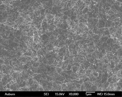
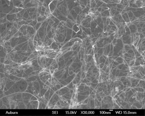
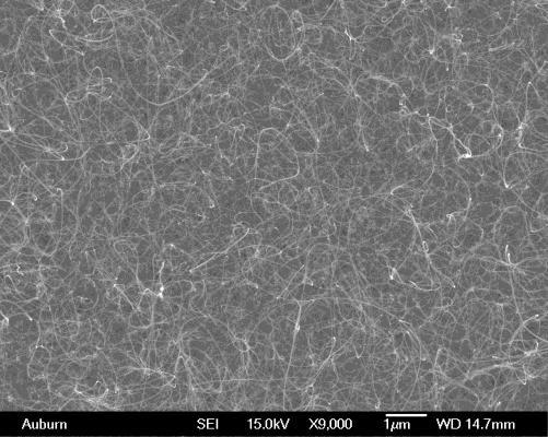

61 Images of CNTs with 5 min Sputtering (a) 5-10 (b) 5-20 (c)
 5-240")


 10 min (b) 20")
 80 min (e)")

62 (d) 5-80 (e) (f) Figure 3.3: Images of CNTs with 5 min sputtering and growth periods (a) 10 min (b) 20 min (c) 40 min (d) 80 min (e) 120 min (f) 240 min Each set is with resolution of 9000X and 30000X. 52


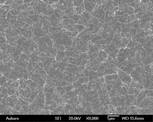

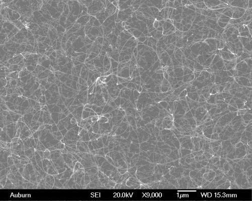

63 Images of CNTs with 10 min Sputtering (a) (b) (c)
 10-240")


 20 min")
 120 min")

64 (d) (e) (f) Figure 3.4: Images of CNTs with 10 min sputtering and growth periods (a) 10 min (b) 20 min (c) 40 min (d) 80 min (e) 120 min (f) 240 min. Each set is with resolution of 9000X and 30000X. 54

")


 30 min")

65 Images of CNTs with 20 min Sputtering (a) (b) (c) Figure 3.5: Images of CNTs with 20 min sputtering and growth periods (a) 20 min (b) 30 min (c) 40 min. Each set is with resolution of 9000X and 30000X. 55

66 3.3 Electron Field Emission Measurement The CNT samples are loaded into the high vacuum chamber to test their field emission characteristics. The chamber is first pumped by the mechanical pump up to mtorr range and then turbo pump is used to pump down, until the pressure reached to 2x x10-7 Torr range. The electron field emission characteristics of carbon nano tube samples are analyzed by a parallelplate set-up, with the carbon nano tubes sample serving as the electron emitting material, placed on the cathode and a small cylindrical rod with area of collector cm 2 serving as the anode. The sample and the anode are separated by two glass insulating spacers of width 140~150 μm. (a) 56
67 (b) Figure 3.6: Field emission measurement setup (a) Schematic (b) Block diagram Computer controlled DC voltage source and pico-ammeter are used to measure the I E characteristics. A digital DC power supply (Stanford Research Systems PS235) is used to apply a voltage between the anode and cathode. A Keithley 485 pico-ammeter is used to measure the emission current. For large-area cathode, it was usually masked in such a way to allow a known area of electron emission. In these experiments a cylindrical rod acting as anode with known area of cm 2 collecting surface, is exposed to the CNT sample in order to limit the total current flow within the range of the power supply. The measured electron emission current was divided by the exposed area to calculate the field emission current density. Initially the chamber is evacuated to a pressure level of ~5x10⁻⁷ Torr and the field emission characteristics are measured at this vacuum level. Each time the voltage applied from 0 to 1200 V with variable voltage steps depending on the data resolution required in the curve. The field emission curves in vacuum are considered as the base data. Further field emission experiments are carried out in helium and dryair respectively at different pressures ranging from 5x10⁻⁷ to 20x10-3 Torr. The 57
68 pressure of the chamber is varied by inputting the relevant gas each time through gas valves. The field emission data is acquired using the data acquisition system as a function of voltage with respective current. This data is used to plot the field emission curves in the excel spread sheet as a function of current density and electric field. The turn-on electric field and saturation current densities in each case are noted using these plots. In other case the field emission experiments are carried out over 100 runs ( V with variable step voltage, to and fro is considered as one run). These runs are to find the stability exhibited by the CNTs in their characteristics. Similar method as above is used to find the turn on saturation current density. These lifetime test experiments are carried out at 20 mtorr pressure for all the samples to test their stability in their characteristics for high pressure applications. The graphs are plotted to find the change in turn-on electric field and saturation current density with respect to the number of runs. The increase in turn-on electric field and decrease in the current density with the number of runs is noted. All comparisons are made with respect to the field emission curves in vacuum. Experiments are also carried out with constant voltage of 600 V applied for 5hours continuously for the lifetime test, to check the current stability and lifetimes of CNTs. These experiments were carried out at high vacuum conditions and repeated for all the samples with growth periods 10, 20, 40, 80, 120 and 240 min and with two different sputtering times of 5 and 10 min. The degradation in current density is plotted across time to see how long the tubes can withstand constant electric field. The plots for all the samples are presented. 58
69 CHAPTER 4 RESULTS AND DISCUSSION Random aligned multi-walled carbon nano tubes were successfully grown on silicon substrate using chemical vapor deposition method. Nano-tubes with different growth times 10, 20, 40, 80, 120 and 240 min each with set of 5 and 10 min sputtering were grown. These samples were analyzed for their field emission characteristics under different pressure conditions in Helium and dryair. Effects of gas pressures on the field emission properties were investigated and analyzed. A series of field emission experiments with 100 runs were performed on each of these samples at 20 mtorr to find the change in turn-on electric field and saturation current density. These results explained the stability exhibited by the CNTs in their field emission characteristics at high pressure conditions. The lifetime and current stability of all the CNT samples were also tested at high vacuum with constant voltage of 600 V applied to all the samples. Samples with sputtering time 20 min were also grown with 20, 30 and 40 min. These entire samples consisted of impurity clusters such as polydedral graphite nano-particles in the CNTs. Field emission experiments were carried out on these samples to test whether the clusters contribute as the electron emitters with nanotubes or not. Life time stability test were also conducted at vacuum for 100 or more runs to see the stability in their characteristics for turn-on and current density. 59
70 4.1 Growth of MWNTs and their Field Emission In this work we have used thermal CVD method to grow CNTs on <100> silicon wafer with Fe as catalyst approximately 50 nm thick. The SEM image of sputtered wafer is given in Figure 3.1. Though the adhesion of sputtering with Fe catalyst is not very good as electron-beam evaporated Ti/Si/Fe catalyst system, high density of CNTs can also achieved by increasing the growth period [91]. In this research, high density MWNTs with long nanotubes achieved with longer growth periods such as 40 min and above. The increase in density of CNTs was observed to be very minimal beyond 40 min growth time, but their field emission characteristics show a reasonable difference in their turn-on, saturation current density and stability in their lifetime. Different definitions such as, the applied electric field when the current reaches 10-7 A, 10-6 A or 10-5 A were considered as the turn-on electric field in the literature. In this case we are defining the turn-on electric field as the applied electric field where the current density starts increasing exponentially from the linear, "dark-current" state. The saturation current density is the maximum current density obtained at the applied electric field at 1200 V power supply. 4.2 Field Emission Characteristics of Random Aligned MWNTs The field emission characteristics of CNTs are tested at different pressures ranging from high vacuum (2x10⁻⁷ Torr) to high pressures (20x10-3 Torr), to observe the change in turn-on electric fields and current densities. These experiments will explain how these CNTs behave when they are used as a cold cathode material of triggering electrode in pseudospark switch at high pressures. Most plasma switches operate in mtorr pressure ranges which are relatively higher 60

71 than the vacuum pressure levels. Therefore the field emission experiments are carried out for the samples with under different pressure conditions in helium and dryair. The following tables show the turn-on electric field and saturation current densities for all the samples for different testing conditions. It can be observed that the turn-on for the CNTs with both 5 min and 10 min sputtering decreases with increase in growth time of the sample. This is observed to be similar case in all different pressures ranging from high vacuum to high pressure. The minimum turn-on field is observed to be 0.53 V/μm for 5 min sputtering and 0.43 V/μm for 10 min sputtering respectively, for the growth time of 240 min sample. But the turn-on field was found to be low for all the cases beyond 20 min growth time. There is definite increase in the saturation current density observed with increase in the growth time for both 5 min and 10 min sputtering cases. The emission characteristics seem to be deteriorating with increase in the pressure levels from 5x10⁻⁷ to 20x10-3 Torr. Table 4.1: Turn-on Electric field for Samples with 5 min sputtering time 61


72 Table 4.2: Saturation current density for samples with 5 min sputtering time Table 4.3:Turn-on Electric field for Samples with 10 min sputtering time Table 4.4: Saturation current density for samples with 10 min sputtering time 62
Introduction to Nanotechnology Chapter 5 Carbon Nanostructures Lecture 1
 Introduction to Nanotechnology Chapter 5 Carbon Nanostructures Lecture 1 ChiiDong Chen Institute of Physics, Academia Sinica chiidong@phys.sinica.edu.tw 02 27896766 Section 5.2.1 Nature of the Carbon Bond
Introduction to Nanotechnology Chapter 5 Carbon Nanostructures Lecture 1
 Introduction to Nanotechnology Chapter 5 Carbon Nanostructures Lecture 1 ChiiDong Chen Institute of Physics, Academia Sinica chiidong@phys.sinica.edu.tw 02 27896766 Carbon contains 6 electrons: (1s) 2,
Carbon nanotubes in a nutshell. Graphite band structure. What is a carbon nanotube? Start by considering graphite.
 Carbon nanotubes in a nutshell What is a carbon nanotube? Start by considering graphite. sp 2 bonded carbon. Each atom connected to 3 neighbors w/ 120 degree bond angles. Hybridized π bonding across whole
Carbon nanotubes in a nutshell
 Carbon nanotubes in a nutshell What is a carbon nanotube? Start by considering graphite. sp 2 bonded carbon. Each atom connected to 3 neighbors w/ 120 degree bond angles. Hybridized π bonding across whole
DEPOSITION OF THIN TiO 2 FILMS BY DC MAGNETRON SPUTTERING METHOD
 Chapter 4 DEPOSITION OF THIN TiO 2 FILMS BY DC MAGNETRON SPUTTERING METHOD 4.1 INTRODUCTION Sputter deposition process is another old technique being used in modern semiconductor industries. Sputtering
2 Symmetry. 2.1 Structure of carbon nanotubes
 2 Symmetry Carbon nanotubes are hollow cylinders of graphite sheets. They can be viewed as single molecules, regarding their small size ( nm in diameter and µm length), or as quasi-one dimensional crystals
TMT4320 Nanomaterials November 10 th, Thin films by physical/chemical methods (From chapter 24 and 25)
") 1 TMT4320 Nanomaterials November 10 th, 2015 Thin films by physical/chemical methods (From chapter 24 and 25) 2 Thin films by physical/chemical methods Vapor-phase growth (compared to liquid-phase growth)
1 TMT4320 Nanomaterials November 10 th, 2015 Thin films by physical/chemical methods (From chapter 24 and 25) 2 Thin films by physical/chemical methods Vapor-phase growth (compared to liquid-phase growth)
Carbon Nanotubes in Interconnect Applications
 Carbon Nanotubes in Interconnect Applications Page 1 What are Carbon Nanotubes? What are they good for? Why are we interested in them? - Interconnects of the future? Comparison of electrical properties
COLD CATHODES FOR APPLICATIONS IN POOR VACUUM AND LOW PRESSURE GAS ENVIRONMENTS: CARBON NANOTUBES VERSUS ZINC OXIDE NANONEEDLES
 COLD CATHODES FOR APPLICATIONS IN POOR VACUUM AND LOW PRESSURE GAS ENVIRONMENTS: CARBON NANOTUBES VERSUS ZINC OXIDE NANONEEDLES Except where reference is made to the work of others, the work described
Metal Deposition. Filament Evaporation E-beam Evaporation Sputter Deposition
 Metal Deposition Filament Evaporation E-beam Evaporation Sputter Deposition 1 Filament evaporation metals are raised to their melting point by resistive heating under vacuum metal pellets are placed on
Fabrication Methods: Chapter 4. Often two methods are typical. Top Down Bottom up. Begins with atoms or molecules. Begins with bulk materials
 Fabrication Methods: Chapter 4 Often two methods are typical Top Down Bottom up Begins with bulk materials Begins with atoms or molecules Reduced in size to nano By thermal, physical Chemical, electrochemical
Chapter 1: Introduction of Carbon Nanotubes: Properties, Synthesis, Characterization and Applications
 Chapter 1: Introduction of Carbon Nanotubes: Properties, Synthesis, Characterization and Applications 1.1. Background 1.2. Introduction of carbon and their allotropes 1.3. Carbon nanotubes (CNTs) 1.4.
Effect of Spiral Microwave Antenna Configuration on the Production of Nano-crystalline Film by Chemical Sputtering in ECR Plasma
 THE HARRIS SCIENCE REVIEW OF DOSHISHA UNIVERSITY, VOL. 56, No. 1 April 2015 Effect of Spiral Microwave Antenna Configuration on the Production of Nano-crystalline Film by Chemical Sputtering in ECR Plasma
Carbon nanotubes synthesis. Ing. Eva Košťáková KNT, FT, TUL
 Carbon nanotubes synthesis Ing. Eva Košťáková KNT, FT, TUL Basic parameters: -Temperature (500, 1000 C ) -Pressure (normal, vacuum ) -Gas (ambient, inert atmosphere nitrogen, argon ) -Time (duration, time
7. Carbon Nanotubes. 1. Overview: Global status market price 2. Types. 3. Properties. 4. Synthesis. MWNT / SWNT zig-zag / armchair / chiral
 7. Carbon Nanotubes 1. Overview: Global status market price 2. Types MWNT / SWNT zig-zag / armchair / chiral 3. Properties electrical others 4. Synthesis arc discharge / laser ablation / CVD 5. Applications
Electrical and Optical Properties. H.Hofmann
 Introduction to Nanomaterials Electrical and Optical Properties H.Hofmann Electrical Properties Ohm: G= σw/l where is the length of the conductor, measured in meters [m], A is the cross-section area of
CARBON NANOTUBES: PYSICAL PROPERTIES & APPLICATIONS
 REPORT TITLE CARBON NANOTUBES: PYSICAL PROPERTIES & APPLICATIONS COURSE NAME: 01NUWKI CHEMISTRY-PHYSICS OF MATERIALS FOR NANOTECHNOLOGY SUBMITTED TO: PROF. GARRONE EDOARDO SUBMITTED BY: NADIA PARVEEN MATRICULATION
Determining Carbon Nanotube Properties from Raman. Scattering Measurements
 Determining Carbon Nanotube Properties from Raman Scattering Measurements Ying Geng 1, David Fang 2, and Lei Sun 3 1 2 3 The Institute of Optics, Electrical and Computer Engineering, Laboratory for Laser
Synthesis of nanotubes. Ewelina Broda
 Synthesis of nanotubes Ewelina Broda Presentation Overview 1. Introduction 2. History 3. Types and structures 4. Properties 5. Synthesis 6. Applications 7. References Allotropes of Elemental Carbon History
Gaetano L Episcopo. Scanning Electron Microscopy Focus Ion Beam and. Pulsed Plasma Deposition
 Gaetano L Episcopo Scanning Electron Microscopy Focus Ion Beam and Pulsed Plasma Deposition Hystorical background Scientific discoveries 1897: J. Thomson discovers the electron. 1924: L. de Broglie propose
Optimization of MnO2 Electrodeposits using Graphenated Carbon Nanotube Electrodes for Supercapacitors
 Optimization of MnO2 Electrodeposits using Graphenated Carbon Nanotube Electrodes for Supercapacitors Waleed Nusrat, 100425398 PHY 3090U Material Science Thursday April 9 th 2015 Researchers optimize the
Table of Content. Mechanical Removing Techniques. Ultrasonic Machining (USM) Sputtering and Focused Ion Beam Milling (FIB)
 Sputtering and Focused Ion Beam Milling (FIB)") Table of Content Mechanical Removing Techniques Ultrasonic Machining (USM) Sputtering and Focused Ion Beam Milling (FIB) Ultrasonic Machining In ultrasonic machining (USM), also called ultrasonic grinding,
Table of Content Mechanical Removing Techniques Ultrasonic Machining (USM) Sputtering and Focused Ion Beam Milling (FIB) Ultrasonic Machining In ultrasonic machining (USM), also called ultrasonic grinding,
Quantized Electrical Conductance of Carbon nanotubes(cnts)
") Quantized Electrical Conductance of Carbon nanotubes(cnts) By Boxiao Chen PH 464: Applied Optics Instructor: Andres L arosa Abstract One of the main factors that impacts the efficiency of solar cells is
Quantized Electrical Conductance of Carbon nanotubes(cnts) By Boxiao Chen PH 464: Applied Optics Instructor: Andres L arosa Abstract One of the main factors that impacts the efficiency of solar cells is
Metallic: 2n 1. +n 2. =3q Armchair structure always metallic = 2
 Properties of CNT d = 2.46 n 2 2 1 + n1n2 + n2 2π Metallic: 2n 1 +n 2 =3q Armchair structure always metallic a) Graphite Valence(π) and Conduction(π*) states touch at six points(fermi points) Carbon Nanotube:
physical Carbon Nanotubes Properties of Physical Properties of Carbon Nanotubes Downloaded from
 physical Properties of Carbon Nanotubes This page is intentionally left blank Rysical Properties of Carbon Nanotubes GDRESSELElAUS & M S DRBSELMUS MZT Imperial College Press Published by Imperial College
Carbon based Nanoscale Electronics
 Carbon based Nanoscale Electronics 09 02 200802 2008 ME class Outline driving force for the carbon nanomaterial electronic properties of fullerene exploration of electronic carbon nanotube gold rush of
Metallic/semiconducting ratio of carbon nanotubes in a bundle prepared using CVD technique
 PRAMANA c Indian Academy of Sciences Vol. 67, No. 2 journal of August 2006 physics pp. 395 400 Metallic/semiconducting ratio of carbon nanotubes in a bundle prepared using CVD technique KHURSHED AHMAD
II.1.4 Nanoengineering of Hybrid Carbon Nanotube-Metal Nanocluster Composite Materials for Hydrogen Storage
 II.1.4 Nanoengineering of Hybrid Carbon Nanotube-Metal Nanocluster Composite Materials for Hydrogen Storage Investigators Kyeongjae (KJ) Cho, Assistant Professor of Mechanical Engineering; Bruce Clemens,
Lecture 6 Plasmas. Chapters 10 &16 Wolf and Tauber. ECE611 / CHE611 Electronic Materials Processing Fall John Labram 1/68
 Lecture 6 Plasmas Chapters 10 &16 Wolf and Tauber 1/68 Announcements Homework: Homework will be returned to you on Thursday (12 th October). Solutions will be also posted online on Thursday (12 th October)
Carbon Nanotubes. Seminar report. Submitted in partial fulfillment of the requirement for the award of degree of Mechanical.
 A Seminar report On Carbon Nanotubes Submitted in partial fulfillment of the requirement for the award of degree of Mechanical SUBMITTED TO: SUBMITTED BY: www.studymafia.org www.studymafia.org Preface
DETECTION OF NH 3 & CO 2 USING CARBON NANOTUBES AT ROOM TEMPERATURE
 International Journal of Nanotechnology and Application (IJNA); ISSN 2277-4777 Vol. 3,Issue 1, Mar 2013, 11-18 TJPRC Pvt.Ltd. DETECTION OF NH 3 & CO 2 USING CARBON NANOTUBES AT ROOM TEMPERATURE G SUDHEER
Carbon Nanotubes: Development of Nanomaterials for Hydrogen Storage
 Carbon Nanotubes: Development of Nanomaterials for Hydrogen Storage Hongjie Dai Department of Chemistry & Laboratory for Advanced Materials Stanford University GCEP, September 19, 2006 Outline Can carbon
What are Carbon Nanotubes? What are they good for? Why are we interested in them?
 Growth and Properties of Multiwalled Carbon Nanotubes What are Carbon Nanotubes? What are they good for? Why are we interested in them? - Interconnects of the future? - our vision Where do we stand - our
In today s lecture, we will cover:
 In today s lecture, we will cover: Metal and Metal oxide Nanoparticles Semiconductor Nanocrystals Carbon Nanotubes 1 Week 2: Nanoparticles Goals for this section Develop an understanding of the physical
CVD: General considerations.
 CVD: General considerations. PVD: Move material from bulk to thin film form. Limited primarily to metals or simple materials. Limited by thermal stability/vapor pressure considerations. Typically requires
Special Properties of Au Nanoparticles
 Special Properties of Au Nanoparticles Maryam Ebrahimi Chem 7500/750 March 28 th, 2007 1 Outline Introduction The importance of unexpected electronic, geometric, and chemical properties of nanoparticles
CARBON NANOSTRUCTURES SYNTHESIZED THROUGH GRAPHITE ETCHING
 CARBON NANOSTRUCTURES SYNTHESIZED THROUGH GRAPHITE ETCHING Q. Yang 1, C. Xiao 1, R. Sammynaiken 2 and A. Hirose 1 1 Plasma Physics Laboratory, University of Saskatchewan, 116 Science Place Saskatoon, SK
Nanostructure. Materials Growth Characterization Fabrication. More see Waser, chapter 2
 Nanostructure Materials Growth Characterization Fabrication More see Waser, chapter 2 Materials growth - deposition deposition gas solid Physical Vapor Deposition Chemical Vapor Deposition Physical Vapor
Plasma Deposition (Overview) Lecture 1
 Lecture 1") Plasma Deposition (Overview) Lecture 1 Material Processes Plasma Processing Plasma-assisted Deposition Implantation Surface Modification Development of Plasma-based processing Microelectronics needs (fabrication
Plasma Deposition (Overview) Lecture 1 Material Processes Plasma Processing Plasma-assisted Deposition Implantation Surface Modification Development of Plasma-based processing Microelectronics needs (fabrication
Wondrous World of Carbon Nanotubes
 Wondrous World of Carbon Nanotubes 2. Synthesis 2.1 Introduction In this section, different techniques for nanotube synthesis and their current status are briefly explained. First, the growth mechanism
Chapter 6. Summary and Conclusions
 Chapter 6 Summary and Conclusions Plasma deposited amorphous hydrogenated carbon films (a-c:h) still attract a lot of interest due to their extraordinary properties. Depending on the deposition conditions
UNIT 3. By: Ajay Kumar Gautam Asst. Prof. Dev Bhoomi Institute of Technology & Engineering, Dehradun
 UNIT 3 By: Ajay Kumar Gautam Asst. Prof. Dev Bhoomi Institute of Technology & Engineering, Dehradun 1 Syllabus Lithography: photolithography and pattern transfer, Optical and non optical lithography, electron,
Thin Film Bi-based Perovskites for High Energy Density Capacitor Applications
 ..SKELETON.. Thin Film Bi-based Perovskites for High Energy Density Capacitor Applications Colin Shear Advisor: Dr. Brady Gibbons 2010 Table of Contents Chapter 1 Introduction... 1 1.1 Motivation and Objective...
Imaging Carbon materials with correlative Raman-SEM microscopy. Introduction. Raman, SEM and FIB within one chamber. Diamond.
 Imaging Carbon materials with correlative Raman-SEM microscopy Application Example Carbon materials are widely used in many industries for their exceptional properties. Electric conductance, light weight,
Supplementary Figure 1 Detailed illustration on the fabrication process of templatestripped
 Supplementary Figure 1 Detailed illustration on the fabrication process of templatestripped gold substrate. (a) Spin coating of hydrogen silsesquioxane (HSQ) resist onto the silicon substrate with a thickness
Chapter 3 Engineering Science for Microsystems Design and Fabrication
 Lectures on MEMS and MICROSYSTEMS DESIGN and MANUFACTURE Chapter 3 Engineering Science for Microsystems Design and Fabrication In this Chapter, we will present overviews of the principles of physical and
Fabrication Technology, Part I
 EEL5225: Principles of MEMS Transducers (Fall 2004) Fabrication Technology, Part I Agenda: Microfabrication Overview Basic semiconductor devices Materials Key processes Oxidation Thin-film Deposition Reading:
Modeling and Performance analysis of Metallic CNT Interconnects for VLSI Applications
 IOSR Journal of Electronics and Communication Engineering (IOSR-JECE) e-issn: 2278-2834, p- ISSN: 2278-8735. Volume 4, Issue 6 (Jan. - Feb. 2013), PP 32-36 Modeling and Performance analysis of Metallic
A new method of growing graphene on Cu by hydrogen etching
 A new method of growing graphene on Cu by hydrogen etching Linjie zhan version 6, 2015.05.12--2015.05.24 CVD graphene Hydrogen etching Anisotropic Copper-catalyzed Highly anisotropic hydrogen etching method
CHAPTER 6: Etching. Chapter 6 1
 Chapter 6 1 CHAPTER 6: Etching Different etching processes are selected depending upon the particular material to be removed. As shown in Figure 6.1, wet chemical processes result in isotropic etching
Repetition: Practical Aspects
 Repetition: Practical Aspects Reduction of the Cathode Dark Space! E x 0 Geometric limit of the extension of a sputter plant. Lowest distance between target and substrate V Cathode (Target/Source) - +
Vacuum Pumps. Two general classes exist: Gas transfer physical removal of matter. Mechanical, diffusion, turbomolecular
 Vacuum Technology Vacuum Pumps Two general classes exist: Gas transfer physical removal of matter Mechanical, diffusion, turbomolecular Adsorption entrapment of matter Cryo, sublimation, ion Mechanical
Carbon Nanotubes. Andrea Goldoni. Elettra- Sincrotrone Trieste S.C.p.A., s.s. 14 Km 163,5 in Area Science Park, Trieste, Italy
 Carbon Nanotubes Andrea Goldoni Elettra- Sincrotrone Trieste S.C.p.A., s.s. 14 Km 163,5 in Area Science Park, 34012 Trieste, Italy Up to 1985 the only two allotropic form of carbon were known: graphite
Graphene The Search For Two Dimensions. Christopher Scott Friedline Arizona State University
 Graphene The Search For Two Dimensions Christopher Scott Friedline Arizona State University What Is Graphene? Single atomic layer of graphite arranged in a honeycomb crystal lattice Consists of sp 2 -bonded
Jin Suk Calvin Kim BACHELOR OF SCIENCE. at the MASSACHUSETTS INSTITUTE OF TECHNOLOGY. May C 2006 JIN SUK CALVIN KIM All rights reserved
 . - The Role of Hydrogen in the Growth of Carbon Nanotubes: A Study of the Catalyst State and Morphology by Jin Suk Calvin Kim Submitted to the Department of Materials Science and Engineering in partial
Carbon Nanotube: The Inside Story
 Krasnoyarsk: 24 th August, 2009 Carbon Nanotube: The Inside Story Review written for Journal of Nanoscience and Nanotechnology Yoshinori ANDO Dean of Faculty of Science and Technology, Meijo University
DEPARTMENT OF ELECTRICAL ENGINEERING DIT UNIVERSITY HIGH VOLTAGE ENGINEERING
 UNIT 1: BREAKDOWN IN SOLIDS 1.) Introduction: The solid dielectric materials are used in all kinds of electrical apparatus and devices to insulate current carrying part from another when they operate at
Nanotechnology 5 th lecture
 Nanotechnology 5 th lecture (c) http://www.nccr-nano.org/nccr_data/ gallery/gallery_01/gallery_01_03/pics_06/ internet/nanotube_spiral.jpg Plan for today: http://www.nccr-nano.org/nccr_data/gallery/ gallery_01/gallery_01_03/pics_04/internet/
Nanotechnology in Consumer Products
 Nanotechnology in Consumer Products June 17, 2015 October 31, 2014 The webinar will begin at 1pm Eastern Time Perform an audio check by going to Tools > Audio > Audio Setup Wizard Chat Box Chat Box Send
Carbon Nanotubes for Interconnect Applications Franz Kreupl, Andrew P. Graham, Maik Liebau, Georg S. Duesberg, Robert Seidel, Eugen Unger
 Carbon Nanotubes for Interconnect Applications Franz Kreupl, Andrew P. Graham, Maik Liebau, Georg S. Duesberg, Robert Seidel, Eugen Unger Infineon Technologies Corporate Research Munich, Germany Outline
Functionalized Carbon Nanotubes a key to nanotechnology?
 1 27th Max Born Symposium Multiscale Modeling of Real Materials Wroclaw, Sep 19, 2010 Functionalized Carbon Nanotubes a key to nanotechnology? Karolina Milowska, Magda Birowska & Jacek A. Majewski Faculty
Carbon nanomaterials. Gavin Lawes Wayne State University.
 Carbon nanomaterials Gavin Lawes Wayne State University glawes@wayne.edu Outline 1. Carbon structures 2. Carbon nanostructures 3. Potential applications for Carbon nanostructures Periodic table from bpc.edu
Energetic particles and their detection in situ (particle detectors) Part II. George Gloeckler
 Part II. George Gloeckler") Energetic particles and their detection in situ (particle detectors) Part II George Gloeckler University of Michigan, Ann Arbor, MI University of Maryland, College Park, MD Simple particle detectors Gas-filled
Energetic particles and their detection in situ (particle detectors) Part II George Gloeckler University of Michigan, Ann Arbor, MI University of Maryland, College Park, MD Simple particle detectors Gas-filled
Modern Methods in Heterogeneous Catalysis Research: Preparation of Model Systems by Physical Methods
 Modern Methods in Heterogeneous Catalysis Research: Preparation of Model Systems by Physical Methods Methods for catalyst preparation Methods discussed in this lecture Physical vapour deposition - PLD
Supplementary Figure S1. AFM image and height profile of GO. (a) AFM image
 AFM image") Supplementary Figure S1. AFM image and height profile of GO. (a) AFM image and (b) height profile of GO obtained by spin-coating on silicon wafer, showing a typical thickness of ~1 nm. 1 Supplementary
Supplementary Figure S1. AFM image and height profile of GO. (a) AFM image and (b) height profile of GO obtained by spin-coating on silicon wafer, showing a typical thickness of ~1 nm. 1 Supplementary
Calculating Electronic Structure of Different Carbon Nanotubes and its Affect on Band Gap
 Calculating Electronic Structure of Different Carbon Nanotubes and its Affect on Band Gap 1 Rashid Nizam, 2 S. Mahdi A. Rizvi, 3 Ameer Azam 1 Centre of Excellence in Material Science, Applied Physics AMU,
We are IntechOpen, the world s leading publisher of Open Access books Built by scientists, for scientists. International authors and editors
 We are IntechOpen, the world s leading publisher of Open Access books Built by scientists, for scientists 3,500 108,000 1.7 M Open access books available International authors and editors Downloads Our
CHAPTER 6 CHIRALITY AND SIZE EFFECT IN SINGLE WALLED CARBON NANOTUBES
 10 CHAPTER 6 CHIRALITY AND SIZE EFFECT IN SINGLE WALLED CARBON NANOTUBES 6.1 PREAMBLE Lot of research work is in progress to investigate the properties of CNTs for possible technological applications.
Nonconventional Technologies Review no. 4/2009
 THE SYNTHESIS OF CARBON NANOTUBES MOŞ Cornelia, ILIEŞ Dorin University of Oradea Abstract : In this article, different techniques for nanotube synthesis and their current status are briefly explained.
Graphene Fundamentals and Emergent Applications
 Graphene Fundamentals and Emergent Applications Jamie H. Warner Department of Materials University of Oxford Oxford, UK Franziska Schaffel Department of Materials University of Oxford Oxford, UK Alicja
Carbon Nanomaterials
 Carbon Nanomaterials STM Image 7 nm AFM Image Fullerenes C 60 was established by mass spectrographic analysis by Kroto and Smalley in 1985 C 60 is called a buckminsterfullerene or buckyball due to resemblance
PHYSICS PAPER 1 (THEORY)
") PHYSICS PAPER 1 (THEORY) (Three hours) (Candidates are allowed additional 15 minutes for only reading the paper. They must NOT start writing during this time.) ---------------------------------------------------------------------------------------------------------------------
PHYSICS PAPER 1 (THEORY) (Three hours) (Candidates are allowed additional 15 minutes for only reading the paper. They must NOT start writing during this time.) ---------------------------------------------------------------------------------------------------------------------
Graphene. Tianyu Ye November 30th, 2011
 Graphene Tianyu Ye November 30th, 2011 Outline What is graphene? How to make graphene? (Exfoliation, Epitaxial, CVD) Is it graphene? (Identification methods) Transport properties; Other properties; Applications;
A NEW APPROACH TOWARDS PROPERTY NANOMEASUREMENTS USING IN-SITU TEM
 A NEW APPROACH TOWARDS PROPERTY NANOMEASUREMENTS USING IN-SITU TEM Z.L. WANG*, P. PONCHARAL**, W.A. DE HEER** and R.P. GAO* * School of Materials Science and Engineering, ** School of Physics, Georgia
LECTURE 5 SUMMARY OF KEY IDEAS
 LECTURE 5 SUMMARY OF KEY IDEAS Etching is a processing step following lithography: it transfers a circuit image from the photoresist to materials form which devices are made or to hard masking or sacrificial
Carbon Nanotubes (CNTs)
") Carbon Nanotubes (s) Seminar: Quantendynamik in mesoskopischen Systemen Florian Figge Fakultät für Physik Albert-Ludwigs-Universität Freiburg July 7th, 2010 F. Figge (University of Freiburg) Carbon Nanotubes
Carbon Nanotubes (s) Seminar: Quantendynamik in mesoskopischen Systemen Florian Figge Fakultät für Physik Albert-Ludwigs-Universität Freiburg July 7th, 2010 F. Figge (University of Freiburg) Carbon Nanotubes
Chapter 5: Nanoparticle Production from Cathode Sputtering. in High-Pressure Microhollow Cathode and Arc Discharges
 96 Chapter 5: Nanoparticle Production from Cathode Sputtering in High-Pressure Microhollow Cathode and Arc Discharges 5.1. Introduction Sputtering is a fundamental aspect of plasma operation and has been
ETCHING Chapter 10. Mask. Photoresist
 ETCHING Chapter 10 Mask Light Deposited Substrate Photoresist Etch mask deposition Photoresist application Exposure Development Etching Resist removal Etching of thin films and sometimes the silicon substrate
MICROCHIP MANUFACTURING by S. Wolf
 by S. Wolf Chapter 15 ALUMINUM THIN-FILMS and SPUTTER-DEPOSITION 2004 by LATTICE PRESS CHAPTER 15 - CONTENTS Aluminum Thin-Films Sputter-Deposition Process Steps Physics of Sputter-Deposition Magnetron-Sputtering
The Q Machine. 60 cm 198 cm Oven. Plasma. 6 cm 30 cm. 50 cm. Axial. Probe. PUMP End Plate Magnet Coil. Filament Cathode. Radial. Hot Plate.
 1 The Q Machine 60 cm 198 cm Oven 50 cm Axial Probe Plasma 6 cm 30 cm PUMP End Plate Magnet Coil Radial Probe Hot Plate Filament Cathode 2 THE Q MACHINE 1. GENERAL CHARACTERISTICS OF A Q MACHINE A Q machine
Stretching the Barriers An analysis of MOSFET Scaling. Presenters (in order) Zeinab Mousavi Stephanie Teich-McGoldrick Aseem Jain Jaspreet Wadhwa
 Zeinab Mousavi Stephanie Teich-McGoldrick Aseem Jain Jaspreet Wadhwa") Stretching the Barriers An analysis of MOSFET Scaling Presenters (in order) Zeinab Mousavi Stephanie Teich-McGoldrick Aseem Jain Jaspreet Wadhwa Why Small? Higher Current Lower Gate Capacitance Higher
Stretching the Barriers An analysis of MOSFET Scaling Presenters (in order) Zeinab Mousavi Stephanie Teich-McGoldrick Aseem Jain Jaspreet Wadhwa Why Small? Higher Current Lower Gate Capacitance Higher
.Fritjaf Capra, The Tao of Physics
 Probing inside the atom and investigating its structure, science transcended the limits of our sensory imagination. From this point on, it could no longer rely with absolute certainty on logic and common
Nanomaterials (II): Carbon Nanotubes
: Carbon Nanotubes") Nanomaterials (II): Carbon Nanotubes Carbon Nanotubes Carbon nanotubes (CNTs) belong to the fullerene family. Fullerenes are composed of covalently boded C atoms arranged to form a closed, convex cage.
Nanomaterials (II): Carbon Nanotubes Carbon Nanotubes Carbon nanotubes (CNTs) belong to the fullerene family. Fullerenes are composed of covalently boded C atoms arranged to form a closed, convex cage.
Supplementary Information
 Supplementary Information Supplementary Figure 1. fabrication. A schematic of the experimental setup used for graphene Supplementary Figure 2. Emission spectrum of the plasma: Negative peaks indicate an
Chapter 10: Liquids, Solids, and Phase Changes
 Chapter 10: Liquids, Solids, and Phase Changes In-chapter exercises: 10.1 10.6, 10.11; End-of-chapter Problems: 10.26, 10.31, 10.32, 10.33, 10.34, 10.35, 10.36, 10.39, 10.40, 10.42, 10.44, 10.45, 10.66,
CITY UNIVERSITY OF HONG KONG. Theoretical Study of Electronic and Electrical Properties of Silicon Nanowires
 CITY UNIVERSITY OF HONG KONG Ë Theoretical Study of Electronic and Electrical Properties of Silicon Nanowires u Ä öä ªqk u{ Submitted to Department of Physics and Materials Science gkö y in Partial Fulfillment
Outline Scanning Probe Microscope (SPM)
") AFM Outline Scanning Probe Microscope (SPM) A family of microscopy forms where a sharp probe is scanned across a surface and some tip/sample interactions are monitored Scanning Tunneling Microscopy (STM)
AFM Outline Scanning Probe Microscope (SPM) A family of microscopy forms where a sharp probe is scanned across a surface and some tip/sample interactions are monitored Scanning Tunneling Microscopy (STM)
Combinatorial RF Magnetron Sputtering for Rapid Materials Discovery: Methodology and Applications
 Combinatorial RF Magnetron Sputtering for Rapid Materials Discovery: Methodology and Applications Philip D. Rack,, Jason D. Fowlkes,, and Yuepeng Deng Department of Materials Science and Engineering University
EE143 Fall 2016 Microfabrication Technologies. Lecture 6: Thin Film Deposition Reading: Jaeger Chapter 6
 EE143 Fall 2016 Microfabrication Technologies Lecture 6: Thin Film Deposition Reading: Jaeger Chapter 6 Prof. Ming C. Wu wu@eecs.berkeley.edu 511 Sutardja Dai Hall (SDH) 1 Vacuum Basics Units 1 atmosphere
The Franck-Hertz Experiment Physics 2150 Experiment No. 9 University of Colorado
 Experiment 9 1 Introduction The Franck-Hertz Experiment Physics 2150 Experiment No. 9 University of Colorado During the late nineteenth century, a great deal of evidence accumulated indicating that radiation
INSTRUMENTATION ECE Fourth Semester. Presented By:- Sumit Grover Lect., Deptt. of ECE
 INSTRUMENTATION ECE Fourth Semester Presented By:- Sumit Grover Lect., Deptt. of ECE Detailed Contents Objectives Sensors and transducer Classification of transducers Temperature transducers Resistance
CHAPTER 2 NANOCARBON PROCESS TECHNOLOGY AND CHARACTERISATION
 CHAPTER 2 NANOCARBON PROCESS TECHNOLOGY AND CHARACTERISATION Carbon, which forms the basis of most of the living organisms, occurs in different allotropic forms such as amorphous carbon, graphene, fullerene,
STM spectroscopy (STS)
") STM spectroscopy (STS) di dv 4 e ( E ev, r) ( E ) M S F T F Basic concepts of STS. With the feedback circuit open the variation of the tunneling current due to the application of a small oscillating voltage
STM spectroscopy (STS) di dv 4 e ( E ev, r) ( E ) M S F T F Basic concepts of STS. With the feedback circuit open the variation of the tunneling current due to the application of a small oscillating voltage
Chapter 7 Plasma Basic
 Chapter 7 Plasma Basic Hong Xiao, Ph. D. hxiao89@hotmail.com www2.austin.cc.tx.us/hongxiao/book.htm Hong Xiao, Ph. D. www2.austin.cc.tx.us/hongxiao/book.htm 1 Objectives List at least three IC processes
6.5 Optical-Coating-Deposition Technologies
 92 Chapter 6 6.5 Optical-Coating-Deposition Technologies The coating process takes place in an evaporation chamber with a fully controlled system for the specified requirements. Typical systems are depicted
E SC 412 Nanotechnology: Materials, Infrastructure, and Safety Wook Jun Nam
 E SC 412 Nanotechnology: Materials, Infrastructure, and Safety Wook Jun Nam Lecture 10 Outline 1. Wet Etching/Vapor Phase Etching 2. Dry Etching DC/RF Plasma Plasma Reactors Materials/Gases Etching Parameters
METAL/CARBON-NANOTUBE INTERFACE EFFECT ON ELECTRONIC TRANSPORT
 METAL/CARBON-NANOTUBE INTERFACE EFFECT ON ELECTRONIC TRANSPORT S. Krompiewski Institute of Molecular Physics, Polish Academy of Sciences, M. Smoluchowskiego 17, 60-179 Poznań, Poland OUTLINE 1. Introductory
COMPARISON OF J-E CHARACTERISTICS OF A CNT BASED COLD CATHODE GROWN BY CVD AND PECVD
 International Journal of Physics and Research (IJPR) ISSN 2250-0030 Vol.3, Issue 1, Mar 2013, 17-22 TJPRC Pvt. Ltd. COMPARISON OF J-E CHARACTERISTICS OF A CNT BASED COLD CATHODE GROWN BY CVD AND PECVD
CHAPTER 13. States of Matter. Kinetic = motion. Polar vs. Nonpolar. Gases. Hon Chem 13.notebook
 CHAPTER 13 States of Matter States that the tiny particles in all forms of matter are in constant motion. Kinetic = motion A gas is composed of particles, usually molecules or atoms, with negligible volume
Selective Manipulation of Molecules by Electrostatic Force and Detection of Single Molecules in Aqueous Solution
 Supporting Information Selective Manipulation of Molecules by Electrostatic Force and Detection of Single Molecules in Aqueous Solution Zhongbo Yan, Ming Xia, Pei Zhang, and Ya-Hong Xie* Department of