COMSOL Design Tool: Simulations of Optical Components Week 6: Waveguides and propagation S matrix
|
|
|
- Edwina Curtis
- 5 years ago
- Views:
Transcription

1 COMSOL Design Tool: Simulations of Optical Components Week 6: Waveguides and propagation S matrix Nikola Dordevic and Yannick Salamin
2 Content Revision Wave Propagation Losses Wave Propagation Examples Dielectric Slab Quantitative analysis of photonics system S matrix Transmission Reflection Scattering losses Example Bending radius of a waveguide

3 Homework - Mode solver For a confined mode, no energy flow in the radial direction: n n eff Wave cannot be evanescent in the core region: n n n 2 1 eff 2 Core r = 8um n = Cladding r = 40um n = n 2 n


4 Step Fiber Mode - solution LP01 LP11 HE11 TE01 TM


5 Waveguide Out-of-plane In-plane
 In-plane: Port need to be defined (eigenvalue solution to defined")

6 Revision Propagation Out-of-plane : Port aren t defined (eigenvalue solution to whole geometry) In-plane: Port need to be defined (eigenvalue solution to defined port) Out of plane Excitation from surface plane Electromagnetics node: NO PORT In plane Port Excitation from boundary Electromagnetics node: TE or TM
7 Revision Effective index n eff n 2 n 1 n 2 Cladding Core Cladding n 2 < n eff < n 1 (1) Only 1 material More materials n mode == n material Maxwell s Laws (Field Continuity) n eff close n 1 Most power in core (confinement) n eff close n 2 Most power in substrate/superstrate Field must have a continuous profile across interface
8 Revision Types of modes (z-propagation) Planar (infinite parallel plates) TE No E z. Only E y (or E x ), H x (or H y ) and H z TM No H z. Only E y (or E x ), H x (or H y ) and E z Dielectric Waveguides TE TM Mix of TE & TM All components Fundamental In reality modes are quasi-te or quasi-tm
 But how does a propagating wave look in Comsol?? 30.10.")
9 Wave Propagation - revision Dielectric Slab What we want Propagation in core Decay (exponential) in sub/superstrate High confinement What we don t want Propagation in sub/superstrate Low confinement (except in certain application - e.g Couplers) But how does a propagating wave look in Comsol??
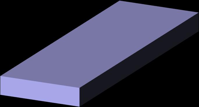
10 Dielectric Slab Waveguide 2D n core = 1.5 n cladding = 1 λ = 1550nm 2 2d 2 2 M n1 n2 d n n n n d = 1um

11 Wave Propagation Examples Dielectric slab waveguide
 0.333 W b) 0.5 W c) 1 W d) Nah, who cares! P in = 1W 30.10.")
12 Wave propagation quiz We have 1W at the input of our waveguide It s straight We have lossless material Now, the output P out will be a) W b) 0.5 W c) 1 W d) Nah, who cares! P in = 1W


13 Wave propagation Many inputs What happens with system when we have MIMO? Examples How do we calculate those things?
14 S Matrix for photonics How to characterize our photonics system as whole? Scattering matrix (so called S-matrix) output input Superposition: b i = S ij a j j=1..n b 1 b 2 b n = S 11 S 1n S n1 S nn a 1 a 2 a n
15 S parameters for photonics How to characterize our photonics system as whole? S matrix Unitary in lossless systems Diagonal S ii terms are complex valued amplitude reflection coefficients Superposition: b i = j=1..n S ij a j b 1 b 2 b n = S 11 S 1n S n1 S nn a 1 a 2 a n
16 S parameters for photonics How to characterize our photonics system as whole? S matrix Unitary in lossless systems Diagonal S ii terms are complex valued amplitude reflection coefficients Two input/output ports: a 1 b 1 = S 11 S 12 a 1 a 2 b 2 S 21 S 22 a 2 T T = R = b 1 R b
17 S parameters for photonics How to characterize our photonics system as whole? S matrix Unitary in lossless systems Diagonal S ii terms are complex valued amplitude reflection coefficients Two input/output ports: a 1 b 1 = S 11 S 12 a 1 a 2 b 2 S 21 S 22 a 2 T T = S 21 2 R = S 11 2 b 1 R b
18 S parameters for photonics: COMSOL Can COMSOL help? S matrix Luckily, COMSOL has built in calculation of these! Two input/output ports: These are the ports we define in COMSOL! a 1 b 1 = S 11 S 12 a 1 a 2 b 2 S 21 S 22 a 2 T T = S 21 2 R = S 11 2 b 1 R b 2 COMSOL calculates this!
 30.10.")
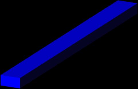
19 Example Tapering Sometimes, photonics design requires that waveguide also changes its width Example is Multi Mode Interference coupler (one of the projects)
20 Homework - Tapering Tasks: Plot transmission curve for different taper lengths (Note: you can add trapezoid in COMSOL) L taper greater then 100 nm SiO 2 L 2 L taper w 1 w 2 L 1 Si
21 Tapering What do you expect to happen?
22 Tapering
23 Tapering What do you expect to happen?
24 Port 2 COMSOL Homework Now, let s see how it works SiO 2 Port 1 Si We will launch 1W at the port 1 We add circular segment with a radius r We collect the power at the port 2 We calculate the transmission Bending radius r
 dx 30.10.")
25 COMSOL Homework Parameters (in_x,dy/2) Si_w dy Si_l (-dx/2,out_y) dx

26 Geometry section

27 Geometry

28 Geometry

29 Geometry

30 Geometry

31 Geometry

32 Geometry

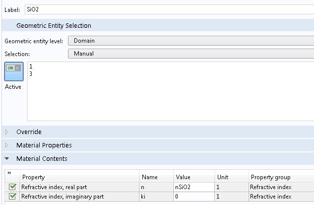
33 Materials

34 Frequency domain We have to initialize ports We want to inject a mode and measure the transmission We want to prevent scattered waves to reflect back into the domain


35 Frequency domain Port


36 Frequency domain Port


37 Mesh definition We want to customize the mesh size!


38 Mesh definition We want to customize the mesh size! We want high resolution inside the curvature!


39 Mesh definition We want to customize the mesh size! We want the remaining part of geometry to be meshed using the regular size

40 Mesh - result
41 Study Parametric sweep we want to change the radius of curvature Boundary of the ports are analyzed and fundamental mode injected (Port 1) and power at the Port 2 is received Propagation at single frequency (wavelength) is analyzed using the Frequency domain

42 Study

43 Study

44 Study


45 Results Transmission for different bending radius
4. Integrated Photonics. (or optoelectronics on a flatland)
") 4. Integrated Photonics (or optoelectronics on a flatland) 1 x Benefits of integration in Electronics: Are we experiencing a similar transformation in Photonics? Mach-Zehnder modulator made from Indium
4. Integrated Photonics (or optoelectronics on a flatland) 1 x Benefits of integration in Electronics: Are we experiencing a similar transformation in Photonics? Mach-Zehnder modulator made from Indium
P&S COMSOL Design Tool Week 3: Simulation Concept
 P&S COMSOL Design Tool Week 3: Simulation Concept Nikola Dordevic, Yannick Salamin Yannick Salamin yannick.salamin@ief.ee.ethz.ch 30.10.2017 1 Content Simulation concept - Homework Matlab examples Intro
Introduction to optical waveguide modes
 Chap. Introduction to optical waveguide modes PHILIPPE LALANNE (IOGS nd année) Chapter Introduction to optical waveguide modes The optical waveguide is the fundamental element that interconnects the various
1 The formation and analysis of optical waveguides
 1 The formation and analysis of optical waveguides 1.1 Introduction to optical waveguides Optical waveguides are made from material structures that have a core region which has a higher index of refraction
Fundamentals of fiber waveguide modes
 SMR 189 - Winter College on Fibre Optics, Fibre Lasers and Sensors 1-3 February 007 Fundamentals of fiber waveguide modes (second part) K. Thyagarajan Physics Department IIT Delhi New Delhi, India Fundamentals
Si Micro-Ring Resonator. Yoojin Ban
 Si Micro-Ring Resonator Yoojin Ban Why Photonics? Copper wires reaching physical limits ~10 Gbps or higher becoming challenging Distance/speed tradeoff shortens lengths Alternative: Transmit data over
Lecture 3 Fiber Optical Communication Lecture 3, Slide 1
 Lecture 3 Optical fibers as waveguides Maxwell s equations The wave equation Fiber modes Phase velocity, group velocity Dispersion Fiber Optical Communication Lecture 3, Slide 1 Maxwell s equations in
Analysis of Single Mode Step Index Fibres using Finite Element Method. * 1 Courage Mudzingwa, 2 Action Nechibvute,
 Analysis of Single Mode Step Index Fibres using Finite Element Method. * 1 Courage Mudzingwa, 2 Action Nechibvute, 1,2 Physics Department, Midlands State University, P/Bag 9055, Gweru, Zimbabwe Abstract
ECE 484 Semiconductor Lasers
 ECE 484 Semiconductor Lasers Dr. Lukas Chrostowski Department of Electrical and Computer Engineering University of British Columbia January, 2013 Module Learning Objectives: Understand the importance of
OPTI510R: Photonics. Khanh Kieu College of Optical Sciences, University of Arizona Meinel building R.626
 OPTI510R: Photonics Khanh Kieu College of Optical Sciences, University of Arizona kkieu@optics.arizona.edu Meinel building R.626 Announcements Homework #4 is assigned, due March 25 th Start discussion
UNIT I ELECTROSTATIC FIELDS
 UNIT I ELECTROSTATIC FIELDS 1) Define electric potential and potential difference. 2) Name few applications of gauss law in electrostatics. 3) State point form of Ohm s Law. 4) State Divergence Theorem.
OPTI510R: Photonics. Khanh Kieu College of Optical Sciences, University of Arizona Meinel building R.626
 OPTI510R: Photonics Khanh Kieu College of Optical Sciences, University of Arizona kkieu@optics.arizona.edu Meinel building R.626 Announceents HW#3 is due next Wednesday, Feb. 21 st No class Monday Feb.
Complete Polarization Control in Multimode Fibers with Polarization and Mode Coupling: Supplementary Information PER
 Complete Polarization Control in Multimode Fibers with Polarization and Mode Coupling: Supplementary Information Wen Xiong, Chia Wei Hsu, Yaron Bromberg, 2 Jose Enrique Antonio-Lopez, 3 Rodrigo Amezcua
ECE Spring Prof. David R. Jackson ECE Dept. Notes 6
 ECE 6341 Spring 2016 Prof. David R. Jackson ECE Dept. Notes 6 1 Leaky Modes v TM 1 Mode SW 1 v= utan u ε R 2 R kh 0 n1 r = ( ) 1 u Splitting point ISW f = f s f > f s We will examine the solutions as the
FINITE-DIFFERENCE FREQUENCY-DOMAIN ANALYSIS OF NOVEL PHOTONIC
 FINITE-DIFFERENCE FREQUENCY-DOMAIN ANALYSIS OF NOVEL PHOTONIC WAVEGUIDES Chin-ping Yu (1) and Hung-chun Chang (2) (1) Graduate Institute of Electro-Optical Engineering, National Taiwan University, Taipei,
FIBER OPTICS. Prof. R.K. Shevgaonkar. Department of Electrical Engineering. Indian Institute of Technology, Bombay. Lecture: 07
 FIBER OPTICS Prof. R.K. Shevgaonkar Department of Electrical Engineering Indian Institute of Technology, Bombay Lecture: 07 Analysis of Wave-Model of Light Fiber Optics, Prof. R.K. Shevgaonkar, Dept. of
Surface plasmon polariton propagation around bends at a metal-dielectric interface
 Surface plasmon polariton propagation around bends at a metal-dielectric interface Keisuke Hasegawa, Jens U. Nöckel and Miriam Deutsch Oregon Center for Optics, 1274 University of Oregon, Eugene, OR 97403-1274
ANALYSIS OF THE REFRACTING LEAKY MODES IN D-SHAPED OPTICAL FIBERS
 8 ANALYSIS OF THE REFRACTING LEAKY MOES IN -SHAPE OPTICAL FIBERS Antônio R. Sapienza and Marcelo F. Guimarães State University of Rio de Janeiro Petrobras S. A. Abstract An analytical solution for the
Electromagnetic waves in free space
 Waveguide notes 018 Electromagnetic waves in free space We start with Maxwell s equations for an LIH medum in the case that the source terms are both zero. = =0 =0 = = Take the curl of Faraday s law, then
Step index planar waveguide
 N. Dubreuil S. Lebrun Exam without document Pocket calculator permitted Duration of the exam: 2 hours The exam takes the form of a multiple choice test. Annexes are given at the end of the text. **********************************************************************************
REFLECTION AND REFRACTION AT A SINGLE INTERFACE
 REFLECTION AND REFRACTION AT A SINGLE INTERFACE 5.1 THE BEHAVIOUR OF LIGHT AT A DIELECTRIC INTERFACE The previous Chapters have been concerned with the propagation of waves in empty space or in uniform,
IN conventional optical fibers, light confinement is achieved
 428 JOURNAL OF LIGHTWAVE TECHNOLOGY, VOL. 20, NO. 3, MARCH 2002 Asymptotic Matrix Theory of Bragg Fibers Yong Xu, George X. Ouyang, Reginald K. Lee, Member, IEEE, and Amnon Yariv, Life Fellow, IEEE Abstract
Electromagnetic Theory for Microwaves and Optoelectronics
 Keqian Zhang Dejie Li Electromagnetic Theory for Microwaves and Optoelectronics Translated by authors With 259 Figures Springer Contents 1 Basic Electromagnetic Theory 1 1.1 Maxwell's Equations 1 1.1.1
Simulations of nanophotonic waveguides and devices using COMSOL Multiphysics
 Presented at the COMSOL Conference 2010 China Simulations of nanophotonic waveguides and devices using COMSOL Multiphysics Zheng Zheng Beihang University 37 Xueyuan Road, Beijing 100191, China Acknowledgement
CHAPTER 9 ELECTROMAGNETIC WAVES
 CHAPTER 9 ELECTROMAGNETIC WAVES Outlines 1. Waves in one dimension 2. Electromagnetic Waves in Vacuum 3. Electromagnetic waves in Matter 4. Absorption and Dispersion 5. Guided Waves 2 Skip 9.1.1 and 9.1.2
Modeling of a 2D Integrating Cell using CST Microwave Studio
 Modeling of a 2D Integrating Cell using CST Microwave Studio Lena Simone Fohrmann, Gerrit Sommer, Alexander Yu. Petrov, Manfred Eich, CST European User Conference 2015 1 Many gases exhibit absorption lines
Optical Fiber Signal Degradation
 Optical Fiber Signal Degradation Effects Pulse Spreading Dispersion (Distortion) Causes the optical pulses to broaden as they travel along a fiber Overlap between neighboring pulses creates errors Resulting
Optics, Optoelectronics and Photonics
 Optics, Optoelectronics and Photonics Engineering Principles and Applications Alan Billings Emeritus Professor, University of Western Australia New York London Toronto Sydney Tokyo Singapore v Contents
Optimum Access Waveguide Width for 1xN Multimode. Interference Couplers on Silicon Nanomembrane
 Optimum Access Waveguide Width for 1xN Multimode Interference Couplers on Silicon Nanomembrane Amir Hosseini 1,*, Harish Subbaraman 2, David Kwong 1, Yang Zhang 1, and Ray T. Chen 1,* 1 Microelectronic
Title. Author(s) 牧野, 俊太郎. Issue Date DOI. Doc URL. Type. File Information /doctoral.k
 牧野, 俊太郎. Issue Date DOI. Doc URL. Type. File Information /doctoral.k") Title A Study on Nonlinear Optical Devices Based on One-Di Author(s) 牧野, 俊太郎 Issue Date 2016-03-24 DOI 10.14943/doctoral.k12194 Doc URL http://hdl.handle.net/2115/61764 Type theses (doctoral) File Information
Title A Study on Nonlinear Optical Devices Based on One-Di Author(s) 牧野, 俊太郎 Issue Date 2016-03-24 DOI 10.14943/doctoral.k12194 Doc URL http://hdl.handle.net/2115/61764 Type theses (doctoral) File Information
Department of Physics Preliminary Exam January 2 5, 2013
 Department of Physics Preliminary Exam January 2 5, 2013 Day 2: Electricity, Magnetism and Optics Thursday, January 3, 2013 9:00 a.m. 12:00 p.m. Instructions: 1. Write the answer to each question on a
Electromagnetic Wave Guidance Mechanisms in Photonic Crystal Fibers
 Electromagnetic Wave Guidance Mechanisms in Photonic Crystal Fibers Tushar Biswas 1, Shyamal K. Bhadra 1 1 Fiber optics and Photonics Division, CSIR-Central Glass and Ceramic Research Institute *196, Raja
Numerical Analysis of Low-order Modes in Thermally Diffused Expanded Core (TEC) Fibers
 Fibers") Proceedings of the 4th WSEAS Int. Conference on Electromagnetics, Wireless and Optical Communications, Venice, Italy, November 2-22, 26 26 Numerical Analysis of Low-order Modes in Thermally Diffused Expanded
Proceedings of the 4th WSEAS Int. Conference on Electromagnetics, Wireless and Optical Communications, Venice, Italy, November 2-22, 26 26 Numerical Analysis of Low-order Modes in Thermally Diffused Expanded
POLARIZATION OF LIGHT
 POLARIZATION OF LIGHT OVERALL GOALS The Polarization of Light lab strongly emphasizes connecting mathematical formalism with measurable results. It is not your job to understand every aspect of the theory,
Theory of Optical Waveguide
 Theor of Optical Waveguide Class: Integrated Photonic Devices Time: Fri. 8:am ~ :am. Classroom: 資電 6 Lecturer: Prof. 李明昌 (Ming-Chang Lee Reflection and Refraction at an Interface (TE n kˆi H i E i θ θ
Chap. 1 Fundamental Concepts
 NE 2 Chap. 1 Fundamental Concepts Important Laws in Electromagnetics Coulomb s Law (1785) Gauss s Law (1839) Ampere s Law (1827) Ohm s Law (1827) Kirchhoff s Law (1845) Biot-Savart Law (1820) Faradays
Surface Plasmon Polaritons on Metallic Surfaces
 Surface Plasmon Polaritons on Metallic Surfaces Masud Mansuripur, Armis R. Zakharian and Jerome V. Moloney Recent advances in nano-fabrication have enabled a host of nano-photonic experiments involving
Lect. 15: Optical Fiber
 3-dimentioanl dielectric waveguide? planar waveguide circular waveguide optical fiber Optical Fiber: Circular dielectric waveguide made of silica (SiO ) y y n n 1 n Cladding Core r z Fiber axis SiO :Ge
Electromagnetic Theory for Microwaves and Optoelectronics
 Keqian Zhang Dejie Li Electromagnetic Theory for Microwaves and Optoelectronics Second Edition With 280 Figures and 13 Tables 4u Springer Basic Electromagnetic Theory 1 1.1 Maxwell's Equations 1 1.1.1
Lecture Outline 9/27/2017. EE 4347 Applied Electromagnetics. Topic 4a
 9/7/17 Course Instructor Dr. Raymond C. Rumpf Office: A 337 Phone: (915) 747 6958 E Mail: rcrumpf@utep.edu EE 4347 Applied Electromagnetics Topic 4a Transmission Lines Transmission These Lines notes may
Back to basics : Maxwell equations & propagation equations
 The step index planar waveguide Back to basics : Maxwell equations & propagation equations Maxwell equations Propagation medium : Notations : linear Real fields : isotropic Real inductions : non conducting
Surface plasmon waveguides
 Surface plasmon waveguides Introduction Size Mismatch between Scaled CMOS Electronics and Planar Photonics Photonic integrated system with subwavelength scale components CMOS transistor: Medium-sized molecule
Supplementary Figure 1: SAW transducer equivalent circuit
 Supplementary Figure : SAW transducer equivalent circuit Supplementary Figure : Radiation conductance and susceptance of.6um IDT, experiment & calculation Supplementary Figure 3: Calculated z-displacement
Contents. 1 Basic Equations 1. Acknowledgment. 1.1 The Maxwell Equations Constitutive Relations 11
 Preface Foreword Acknowledgment xvi xviii xix 1 Basic Equations 1 1.1 The Maxwell Equations 1 1.1.1 Boundary Conditions at Interfaces 4 1.1.2 Energy Conservation and Poynting s Theorem 9 1.2 Constitutive
Modelling of Ridge Waveguide Bends for Sensor Applications
 Modelling of Ridge Waveguide Bends for Sensor Applications Wilfrid Pascher FernUniversität, Hagen, Germany n 1 n2 n 3 R Modelling of Ridge Waveguide Bends for Sensor Applications Wilfrid Pascher FernUniversität,
MODE THEORY FOR STEP INDEX MULTI-MODE FIBERS. Evgeny Klavir. Ryerson University Electrical And Computer Engineering
 MODE THEORY FOR STEP INDEX MULTI-MODE FIBERS Evgeny Klavir Ryerson University Electrical And Computer Engineering eklavir@ee.ryerson.ca ABSTRACT Cladding n = n This project consider modal theory for step
Optical modes of dielectric spheres (Microsphere Resonators)
") 8 Chapter 2 Optical modes of dielectric spheres (Microsphere Resonators) 2.1 Introduction The modes of a spherical dielectric particle were first investigated by Mie at the beginning of the 19 century,
8 Chapter 2 Optical modes of dielectric spheres (Microsphere Resonators) 2.1 Introduction The modes of a spherical dielectric particle were first investigated by Mie at the beginning of the 19 century,
Study of Propagating Modes and Reflectivity in Bragg Filters with AlxGa1-xN/GaN Material Composition
 Study of Propagating Modes and Reflectivity in Bragg Filters with AlxGa1-xN/GaN Material Composition Sourangsu Banerji Department of Electronics & Communication Engineering, RCC Institute of Information
S-matrix approach for calculations of the optical properties of metallic-dielectric photonic crystal slabs
 S-matrix approach for calculations of the optical properties of metallic-dielectric photonic crystal slabs N. I. Komarevskiy1,2, T. Weiss3, and S. G. Tikhodeev2 1 Faculty of Physics, Lomonosov Moscow State
Cylindrical Dielectric Waveguides
 03/02/2017 Cylindrical Dielectric Waveguides Integrated Optics Prof. Elias N. Glytsis School of Electrical & Computer Engineering National Technical University of Athens Geometry of a Single Core Layer
Drawbacks in Metallic Waveguides. α f. Skin effect. Surface roughness Mono-mode operation Narrow band in metallic rectangular waveguide
 Drawbacks in Metallic Waveguides Skin effect α f Surface roughness Mono-mode operation 1 Narrow band in metallic rectangular waveguide 2 α f α 3 f 2 to f 5 2 Types of Dielectric Waveguide ε r2 (a) Circular
Electromagnetic fields and waves
 Electromagnetic fields and waves Maxwell s rainbow Outline Maxwell s equations Plane waves Pulses and group velocity Polarization of light Transmission and reflection at an interface Macroscopic Maxwell
A COMPACT POLARIZATION BEAM SPLITTER BASED ON A MULTIMODE PHOTONIC CRYSTAL WAVEGUIDE WITH AN INTERNAL PHOTONIC CRYSTAL SECTION
 Progress In Electromagnetics Research, PIER 103, 393 401, 2010 A COMPACT POLARIZATION BEAM SPLITTER BASED ON A MULTIMODE PHOTONIC CRYSTAL WAVEGUIDE WITH AN INTERNAL PHOTONIC CRYSTAL SECTION Y. C. Shi Centre
CST EM : Examples. Chang-Kyun PARK (Ph. D. St.) Thin Films & Devices (TFD) Lab.
 Thin Films & Devices (TFD) Lab.") CST Advanced Training 2004 @ Daedeok Convention Town (2004.03.24) CST EM : Examples TM EM Studio TM Chang-Kyun PARK (Ph. D. St.) E-mail: ckpark@ihanyang.ac.kr Thin Films & Devices (TFD) Lab. Dept. of Electrical
CST Advanced Training 2004 @ Daedeok Convention Town (2004.03.24) CST EM : Examples TM EM Studio TM Chang-Kyun PARK (Ph. D. St.) E-mail: ckpark@ihanyang.ac.kr Thin Films & Devices (TFD) Lab. Dept. of Electrical
Chapter - 7 Power Dividers and Couplers
 4/0/00 7_ Basic Properties of Dividers and Couplers.doc / Chapter - 7 Power Dividers and Couplers One of the most fundamental problems in microwave engineering is how to efficiently divide signal power..0
Virtual Prototype of a Dielectric Window for High Power Microwave Tubes
 Virtual Prototype of a Dielectric Window for High Power Microwave Tubes Alberto Leggieri, Davide Passi and Franco Di Paolo Università degli Studi di Roma Tor Vergata, Department of Electronic Engineering,
Air Force Research Laboratory
 Air Force Research Laboratory Materials with Engineered Dispersion for the Enhancement of Light-Matter Interactions 10 January 2013 Ilya Vitebskiy, AFRL/RYDP Integrity Service Excellence SUBTOPIC 1 Nonreciprocal
Advanced techniques Local probes, SNOM
 Advanced techniques Local probes, SNOM Principle Probe the near field electromagnetic field with a local probe near field probe propagating field evanescent Advanced techniques Local probes, SNOM Principle
Fiber Optics. Equivalently θ < θ max = cos 1 (n 0 /n 1 ). This is geometrical optics. Needs λ a. Two kinds of fibers:
. This is geometrical optics. Needs λ a. Two kinds of fibers:") Waves can be guided not only by conductors, but by dielectrics. Fiber optics cable of silica has nr varying with radius. Simplest: core radius a with n = n 1, surrounded radius b with n = n 0 < n 1. Total
Waves can be guided not only by conductors, but by dielectrics. Fiber optics cable of silica has nr varying with radius. Simplest: core radius a with n = n 1, surrounded radius b with n = n 0 < n 1. Total
J10M.1 - Rod on a Rail (M93M.2)
") Part I - Mechanics J10M.1 - Rod on a Rail (M93M.2) J10M.1 - Rod on a Rail (M93M.2) s α l θ g z x A uniform rod of length l and mass m moves in the x-z plane. One end of the rod is suspended from a straight
Part I - Mechanics J10M.1 - Rod on a Rail (M93M.2) J10M.1 - Rod on a Rail (M93M.2) s α l θ g z x A uniform rod of length l and mass m moves in the x-z plane. One end of the rod is suspended from a straight
Finite Element Method (FEM)
") Finite Element Method (FEM) The finite element method (FEM) is the oldest numerical technique applied to engineering problems. FEM itself is not rigorous, but when combined with integral equation techniques
Finite Element Method (FEM) The finite element method (FEM) is the oldest numerical technique applied to engineering problems. FEM itself is not rigorous, but when combined with integral equation techniques
SUPPLEMENTARY INFORMATION
 In the format provided by the authors and unedited. SUPPLEMENTARY INFORMATION DOI: 10.1038/NPHOTON.017.65 Imaging exciton-polariton transport in MoSe waveguides F. Hu 1,, Y. Luan 1,, M. E. Scott 3, J.
Sub-wavelength electromagnetic structures
 Sub-wavelength electromagnetic structures Shanhui Fan, Z. Ruan, L. Verselegers, P. Catrysse, Z. Yu, J. Shin, J. T. Shen, G. Veronis Ginzton Laboratory, Stanford University http://www.stanford.edu/group/fan
Photonic/Plasmonic Structures from Metallic Nanoparticles in a Glass Matrix
 Excerpt from the Proceedings of the COMSOL Conference 2008 Hannover Photonic/Plasmonic Structures from Metallic Nanoparticles in a Glass Matrix O.Kiriyenko,1, W.Hergert 1, S.Wackerow 1, M.Beleites 1 and
Guided and defect modes in periodic dielectric waveguides
 Fan et al. Vol. 12, No. 7/July 1995/J. Opt. Soc. Am. B 1267 Guided and defect modes in periodic dielectric waveguides Shanhui Fan, Joshua N. Winn, Adrian Devenyi, J. C. Chen, Robert D. Meade, and J. D.
1 Lectures 10 and 11: resonance cavities
 1 1 Lectures 10 and 11: resonance cavities We now analyze cavities that consist of a waveguide of length h, terminated by perfectly conducting plates at both ends. The coordinate system is oriented such
Interferometric model for phase analysis in fiber couplers
 Interferometric model for phase analysis in fiber couplers Xiaojun Fang, Richard O. Claus, and Guy Indebetouw An interferometric model is proposed to estimate the phase differences in lossless, strongly
Electromagnetic Waves
 Electromagnetic Waves Maxwell s equations predict the propagation of electromagnetic energy away from time-varying sources (current and charge) in the form of waves. Consider a linear, homogeneous, isotropic
National Radio Astronomy Observatory EDTN 211. Effects of Misalignment of Square Waveguide Joints. A. R. Kerr 12 March 2009
 National Radio Astronomy Observatory EDTN 211 Effects of Misalignment of Square Waveguide Joints A. R. Kerr 12 March 2009 Abstract: The effects of misalignment between two square waveguides are examined
Lecture 9: Introduction to Diffraction of Light
 Lecture 9: Introduction to Diffraction of Light Lecture aims to explain: 1. Diffraction of waves in everyday life and applications 2. Interference of two one dimensional electromagnetic waves 3. Typical
Nanoscale confinement of photon and electron
 Nanoscale confinement of photon and electron Photons can be confined via: Planar waveguides or microcavities (2 d) Optical fibers (1 d) Micro/nano spheres (0 d) Electrons can be confined via: Quantum well
OPTI510R: Photonics. Khanh Kieu College of Optical Sciences, University of Arizona Meinel building R.626
 OPTI510R: Photonics Khanh Kieu College of Optical Sciences, University of Arizona kkieu@optics.arizona.edu Meinel building R.626 Announcements HW#3 is assigned due Feb. 20 st Mid-term exam Feb 27, 2PM
FINAL EXAM IN FYS-3007
 Page 1 of 4 pages + chart FINAL EXAM IN FYS-007 Exam in : Fys-007 Microwave Techniques Date : Tuesday, May 1, 2011 Time : 09.00 1.00 Place : Åsgårdveien 9 Approved remedies : All non-living and non-communicating
OPTICAL COMMUNICATIONS
 L21-1 OPTICAL COMMUNICATIONS Free-Space Propagation: Similar to radiowaves (but more absorption by clouds, haze) Same expressions: antenna gain, effective area, power received Examples: TV controllers,
PHY3128 / PHYM203 (Electronics / Instrumentation) Transmission Lines
 Transmission Lines") Transmission Lines Introduction A transmission line guides energy from one place to another. Optical fibres, waveguides, telephone lines and power cables are all electromagnetic transmission lines. are
Transmission Lines Introduction A transmission line guides energy from one place to another. Optical fibres, waveguides, telephone lines and power cables are all electromagnetic transmission lines. are
ON THE HYBRID FIELD PATTERNS OF HELICAL CLAD DIELECTRIC OPTICAL FIBERS
 Progress In Electromagnetics Research, PIER 91, 69 84, 2009 ON THE HYBRID FIELD PATTERNS OF HELICAL CLAD DIELECTRIC OPTICAL FIBERS A. H. B. M. Safie and P. K. Choudhury Faculty of Engineering Multimedia
Microwave Engineering 3e Author - D. Pozar
 Microwave Engineering 3e Author - D. Pozar Sections 3.6 3.8 Presented by Alex Higgins 1 Outline Section 3.6 Surface Waves on a Grounded Dielectric Slab Section 3.7 Stripline Section 3.8 Microstrip An Investigation
OPTI510R: Photonics. Khanh Kieu College of Optical Sciences, University of Arizona Meinel building R.626
 OPTI510R: Photonics Khanh Kieu College of Optical Sciences, University of Arizona kkieu@optics.arizona.edu Meinel building R.626 Announcements Mid-term exam on Monday, March 6 th Review Properties of light
ECE 604, Lecture 17. October 30, In this lecture, we will cover the following topics: Reflection and Transmission Single Interface Case
 ECE 604, Lecture 17 October 30, 2018 In this lecture, we will cover the following topics: Duality Principle Reflection and Transmission Single Interface Case Interesting Physical Phenomena: Total Internal
Photonic devices for quantum information processing:
 Outline Photonic devices for quantum information processing: coupling to dots, structure design and fabrication Optoelectronics Group, Cavendish Lab Outline Vuckovic s group Noda s group Outline Outline
Wave propagation in optical waveguides
 Wave propagation in optical waveguides Giulio Ciraolo November, 005 Abstract We present a mathematical framework for studying the problem of electromagnetic wave propagation in a -D or 3-D optical waveguide
Adaptive spatial resolution: application to surface plasmon waveguide modes
 Optical and Quantum Electronics (26) Springer 26 DOI 1.17/s1182-6-91-3 Adaptive spatial resolution: application to surface plasmon waveguide modes peter debackere, peter bienstman, roel baets Photonics
Design of a Multi-Mode Interference Crossing Structure for Three Periodic Dielectric Waveguides
 Progress In Electromagnetics Research Letters, Vol. 75, 47 52, 2018 Design of a Multi-Mode Interference Crossing Structure for Three Periodic Dielectric Waveguides Haibin Chen 1, Zhongjiao He 2,andWeiWang
Waves & Oscillations
 Physics 42200 Waves & Oscillations Lecture 32 Electromagnetic Waves Spring 2016 Semester Matthew Jones Electromagnetism Geometric optics overlooks the wave nature of light. Light inconsistent with longitudinal
FEM-BASED METHOD FOR THE SIMULATION OF DIELECTRIC WAVEGUIDE GRATING BIOSENSORS. Swiss Federal Institute of Technology, Zürich CH-8092, Switzerland
 Progress In Electromagnetics Research, Vol. 137, 565 583, 2013 FEM-BASED METHOD FOR THE SIMULATION OF DIELECTRIC WAVEGUIDE GRATING BIOSENSORS Thomas Guillod 1, Florian Kehl 2, 3, 4, *, and Christian Hafner
Lecture 5 Notes, Electromagnetic Theory II Dr. Christopher S. Baird, faculty.uml.edu/cbaird University of Massachusetts Lowell
 Lecture 5 Notes, Electromagnetic Theory II Dr. Christopher S. Baird, faculty.uml.edu/cbaird University of Massachusetts Lowell 1. Waveguides Continued - In the previous lecture we made the assumption that
TM-Radiation From an Obliquely Flanged Parallel-Plate Waveguide
 1534 IEEE TRANSACTIONS ON ANTENNAS AND PROPAGATION, VOL. 50, NO. 11, NOVEMBER 2002 TM-Radiation From an Obliquely Flanged Parallel-Plate Waveguide Jae Yong Kwon, Member, IEEE, Jae Wook Lee, Associate Member,
Hybrid-mode assisted long-distance excitation of short-range surface plasmons in a nanotipenhanced
 Hybrid-mode assisted long-distance excitation of short-range surface plasmons in a nanotipenhanced step-index fiber Supporting Information Alessandro Tuniz 1*, Mario Chemnitz 1,2, Jan Dellith 1, Stefan
Chapter 5. Photonic Crystals, Plasmonics, and Metamaterials
 Chapter 5. Photonic Crystals, Plasmonics, and Metamaterials Reading: Saleh and Teich Chapter 7 Novotny and Hecht Chapter 11 and 12 1. Photonic Crystals Periodic photonic structures 1D 2D 3D Period a ~
Behavior of light at photonic crystal interfaces
 Behavior of light at photonic crystal interfaces Emanuel Istrate, Alexander A. Green, and Edward H. Sargent Department of Electrical and Computer Engineering, University of Toronto, 10 King s College Road,
Finite Element Method
 Appendix A Finite Element Method A.1 Formulation All the analyses of the PCF properties presented in this book have been performed by using the FEM. The FEM allows the PCF cross-section in the transverse
Light-trapping by diffraction gratings in silicon solar cells
 Light-trapping by diffraction gratings in silicon solar cells Silicon: a gift of nature Rudolf Morf, Condensed Matter Theory, Paul Scherrer Institute Benefits from improved absorption Diffraction gratings
Lecture 11: Introduction to diffraction of light
 Lecture 11: Introduction to diffraction of light Diffraction of waves in everyday life and applications Diffraction in everyday life Diffraction in applications Spectroscopy: physics, chemistry, medicine,
Band structure of honeycomb photonic crystal slabs
 JOURNAL OF APPLIED PHYSICS 99, 093102 2006 Band structure of honeycomb photonic crystal slabs Tai-I Weng and G. Y. Guo a Department of Physics, National Taiwan University, Taipei, Taiwan 106, Republic
Waves. Daniel S. Weile. ELEG 648 Waves. Department of Electrical and Computer Engineering University of Delaware. Plane Waves Reflection of Waves
 Waves Daniel S. Weile Department of Electrical and Computer Engineering University of Delaware ELEG 648 Waves Outline Outline Introduction Let s start by introducing simple solutions to Maxwell s equations
Generating Bessel beams by use of localized modes
 992 J. Opt. Soc. Am. A/ Vol. 22, No. 5/ May 2005 W. B. Williams and J. B. Pendry Generating Bessel beams by use of localized modes W. B. Williams and J. B. Pendry Condensed Matter Theory Group, The Blackett
Quantum Photonic Integrated Circuits
 Quantum Photonic Integrated Circuits IHFG Hauptseminar: Nanooptik und Nanophotonik Supervisor: Prof. Dr. Peter Michler 14.07.2016 Motivation and Contents 1 Quantum Computer Basics and Materials Photon
Resonant modes and laser spectrum of microdisk lasers. N. C. Frateschi and A. F. J. Levi
 Resonant modes and laser spectrum of microdisk lasers N. C. Frateschi and A. F. J. Levi Department of Electrical Engineering University of Southern California Los Angeles, California 90089-1111 ABSTRACT
Truly trapped rainbow by utilizing nonreciprocal waveguides
 Truly trapped rainbow by utilizing nonreciprocal waveguides Kexin Liu 1,2 and Sailing He 1,2,* 1. Department of Electromagnetic Engineering, School of Electrical Engineering, KTH Royal Institute of Technology,
arxiv: v1 [physics.atom-ph] 2 Mar 2012
![arxiv: v1 [physics.atom-ph] 2 Mar 2012](/thumbs/72/67735992.jpg "arxiv: v1 [physics.atom-ph] 2 Mar 2012") Nanofiber-Based Double-Helix Dipole Trap for Cold Neutral Atoms arxiv:1203.0499v1 [physics.atom-ph] 2 Mar 2012 Daniel Reitz, Arno Rauschenbeutel Vienna Center for Quantum Science and Technology, Atominstitut,
Nanofiber-Based Double-Helix Dipole Trap for Cold Neutral Atoms arxiv:1203.0499v1 [physics.atom-ph] 2 Mar 2012 Daniel Reitz, Arno Rauschenbeutel Vienna Center for Quantum Science and Technology, Atominstitut,