UHF/RF High-Q Ceramic Capacitors (Available in Non-Magnetic) C (.600" x.400") C (.760" x.760") C (1.30" x 1.
|
|
|
- Clyde Powell
- 5 years ago
- Views:
Transcription


1

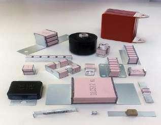
2 New State-of-the-Art Manufacturing Facility over 130,000 square feet of NEW manufacturing area. Established 1988 ISO-9001 Certified ISO Certified MRI-Non-Magnetic Components S-Level Reliability Our products have been widely used in various RF/Microwave Communication Systems, MRI Medical Systems, Broadcast Equipment and various Military Applications Passive Plus, Inc. World Headquarters Huntington, New York USA Ph: (631) Fax: (631)
3 Traditional High Q (>10,000) Low ESR Capacitors (NP0/P90) RF/Microwave Low ESR ESL (NP0/P90) (Available in Non-Magnetic) C/P (.055" x.055") C/P (.110" x.110") C/P (.220" x.250") C/P (.380" x.380") 23 Power Transmitter Capacitors (Q> 10,000) UHF/RF High-Q Ceramic Capacitors (Available in Non-Magnetic) C (.600" x.400") C (.760" x.760") C (1.30" x 1.30") 41 Custom Capacitor Assemblies (Available in Non-Magnetic) 45 EIA Low ESR Microwave Capacitors RF/Microwave NP N (.020" x.010") N (.040" x.020") N (.060" x.030") N (.070" x.080") N (.080" x.050") N (.110" x.110") 83 X7R RF By-Pass Capacitors CONTENTS 0505X (.055 x.055 ) X (.110" x.110") X (.220" x.250") EIA High Q Non-Magnetic Multilayer Ceramic Capacitors Laser Marking Design Kits Broadband Capacitors 01005BB (.010" x.005") 0201BB (.020" x.010") BB (.040" x.020") BB (.080" x.050") 115 Broadband Application Note Notes Soldering Guide

4

5 Traditional High Q (> 10,000) Low ESR Capacitors (NP0 & P90 TC)
, Radar Part Numbering Overview 0505 C 101 J W 151 X TV 1 2 3 4 5 6 7 8")
6 Traditional High Q (>10,000) Low ESR Capacitors Traditional High Q (>10,000) Low ESR Capacitors Product Features High Q, High Power, Low ESR/ESL, Low Noise, High Self-Resonance, Ultra-Stable Performance Typical Applications Field Wireless Broadcasting Equipment, Mobile Base Stations, GPS Portables, Medical (MRI coils), Radar Part Numbering Overview 0505 C 101 J W 151 X TV Tape carrier packing Vertical Orientation Laser Marking Rated Voltage Termination Type Tolerance Rated Capacitance Temperature Coefficient Dimensions Dimensions unit: inch (millimeter) Length ~-.010 ( ~ -0.25) ~ ( ~ -0.25) ~ ( ~ -0.25) ~ ( ~ -0.25) Width.055±.010 (1.4±0.25).110±.010 (2.79±0.25).250±.015 (6.35±0.38).380±.010 (9.65±0.25) Thickness.057(1.45) max.10(2.6) max.165(4.19) max.177(4.5) max Temperature Coefficient: C: 0±30ppm/, P: +90±20ppm/. Rated Capacitance Capacitance is less than 10pF; for example: 1R0=1.0pF, R denotes decimal point. Capacitance greater than 10pF; for example: 101=100pF, the third number is the power of
7 TraditionaI High Q (>10,000) Low ESR Capacitors Tolerance A B C D F G J K M Tolerance ±0.05pF ±0.1pF ±0.25pF ±0.5pF ±1% ±2% ±5% ±10% ±20% Termination Type W P L Type 100% Sn Solder over Nickel Plating 100% Sn Solder over Copper Plating RoHS Compliant 90% Sn10%Pb Solder over Nickel Plating (Tin/Lead) MS AR RR AW RW Type Microstrip Axial Ribbon Radial Ribbon Axial Wire Radial Wire MN AN FN BN RN Type Non-Mag Microstrip Non-Mag Axial Ribbon Non-Mag Radial Ribbon Non-Mag Axial Wire Non-Mag Radial Wire Rated Voltage Rated Voltage Rated Voltage V V V V V V V V V V V V V V Laser Marking X denotes Marking. Capacitance is less than 10pF; for example: the marking of 1.0pF is 1R0. Capacitance greater than 10pF; for example: the marking of 100pF is 101. Packaging Orientation TV: Tape carrier packaging Vertical Orientation. Vertical orientation means that if the part is lifted from the tape without any rotation and placed on a substrate, its electrodes will be perpendicular to the substrate plane. This impacts the frequency of First Parallel Resonance (suckout). Performance Requirements Capacitors are designed and manufactured to meet the requirements of MIL-PRF and MIL-PRF-123. All Products are in Compliance with RoHS Instruction

8 0505C/P (.055 x.055 ) Traditional High Q (>10,000) Low ESR Capacitors 0505C/P (.055 x.055 ) Product Features High Q, High Power, Low ESR/ESL, Low Noise, High Self-Resonance, Ultra-Stable Performance. Product Application Typical Functional Applications: Tuning, Bypass, Coupling, Feedback, D.C. Blocking and Impedance Matching. Typical Circuit Applications: UHF/Microwave RF Power Amplifiers, Mixers, Oscillators, Low Noise Amplifiers, Filter Networks, Timing Circuits and Delay Lines. 0505C/P Capacitance Table NP0=C; P90=P Max. capacitance: 0505P=100pF; 0505C=1000pF Cap. pf 0.1 0R1 Tol. Rated WVDC Cap. pf Tol. Rated WVDC 2.4 2R4 Cap. pf Remark: special capacitance, tolerance and WVDC are available, consult with PASSIVE PLUS. * - Available in NP0 only. Tol. Rated WVDC Cap. pf * 0.2 0R R * 0.3 0R R V * 0.4 0R R * R R6 A,B, * or 0.6 0R R9 C,D * 300V 0.7 0R R * 0.8 0R R * 0.9 0R9 150V 5.1 5R1 150V * 1.0 1R R * R1 A,B, 6.2 6R F,G, * or or 1.2 1R2 C,D 6.8 6R J,K * 300V 300V 1.3 1R R * 1.4 1R4 150V R * 1.5 1R R * R * or 1.7 1R * 200V 1.8 1R F,G, * 1.9 1R * J,K * 2.0 2R * * 2.1 2R * 2.2 2R * Tol. F,G, J,K Rated WVDC 150V 151 or 200V V V 500 or 100V PPI0505CPDATA062518RevA
9 Traditional High Q (>10,000) Low ESR Capacitors Part Numbering 0505C 100 J W 151 X TV 0505C/P (.055 x.055 ) C=NP0; P=P90 Add TV for Vertical Orientation Capacitor 100=10x10 0 =10pF; 1R0=1.0pF Capacitance Tolerance: See below list Laser Marking Rated Voltage Termination Type Capacitance Tolerance A B C D F G J K Tolerance ±0.05pF ±0.1pF ±0.25pF ±0.5pF ±1% ±2% ±5% ±10% 0505C/P Magnetic and Non-Magnetic Dimensions unit:inch(millimeter) Capacitor Dimensions Series Term. Type/Outlines Length Lc Width Wc Thickness Tc Overlap B Plated Material 0505C 0505P W 100%Sn Solder over Nickel Plating RoHS Compliant 0505C 0505P L Chip to ( to -0.25).055±.010 (1.40±0.25).057 (1.45max).020 (0.51max) 90%Sn10%P b Tin/Lead Solder over Nickel Plating 0505C 0505P P (Non-Mag) Chip (Non-Mag) 100%Sn Solder over Copper Plating RoHS Compliant Note: Non-Mag means no magnetic materials PPI0505CPDATA062518RevA
10 Performance Traditional High Q (>10,000) Low ESR Capacitors 0505C/P (.055 x.055 ) Item Specifications Quality Factor (Q) greater than 10,000 at 1MHz. Insulation Resistance (IR) Rated Voltage Dielectric Withstanding Voltage (DWV) 10 5 Megohms +25 at rated WVDC Megohms +125 at rated WVDC. See Rated Voltage Table. 250% of rated Voltage for 5 seconds. Operating Temperature Range -55 to +200 Temperature coefficient (TC) Capacitance Drift Piezoelectric Effects Termination Type C: 0±30ppm/ ; P: +90±20ppm/ ±0.02% or ±0.02pF, whichever is greater. None See Termination Type Table. Capacitors are designed and manufactured to meet the requirements of MIL-PRF and MIL-PRF-123. Environmental Tests Item Specifications Method Thermal shock Moisture resistance Humidity (steady state) Life Terminal strength DWV: the initial value IR: Shall not be less than 30% of the initial value Capacitance change: no more than 0.5% or 0.5 pf, whichever is greater. DWV: the initial value IR: the initial value Capacitance change: no more than 0.3% or 0.3pF, whichever is greater. IR: Shall not be less than 30% of the initial value Capacitance change: no more than 2.0% or 0.5pF, whichever is greater. Force : 10lbs typical, 5 lbs min., Duration time: 5 to 10 seconds. MIL-STD-202, Method 107, Condition A. At the maximum rated temperature (-55 and 200 ) stay 30 min,the time of removing shall not be more than 3 minutes. Perform the five cycles. MIL-STD-202, Method 106. MIL-STD-202, Method 103, Condition A, With 1.5 Volts D.C. applied while subjected to an environment of 85 with 85% relative humidity for 240 hours minimum. MIL-STD-202, Method 108, for 2000 hours, at % Rated voltage D.C. applies. MIL-STD-202, Method 211A, Test condition A. Applied a force and maintained for a period of 5 to 10 seconds. The force shall be in the direction of the axes of the terminations PPI0505CPDATA062518RevA
 0505C/P Q vs Capacitance")

11 0505C/P Performance Curves 0505C/P ESR vs Capacitance Traditional High Q (>10,000) Low ESR Capacitors 0505C/P (.055 x.055 ) 0505C/P Q vs Capacitance 0505C ESR vs Capacitance 0505C Q vs Capacitance Definitions and Measurement Conditions For a capacitor in a series configuration, i.e., mounted across a gap in a microstrip trace, with 50-Ohm source and termination resistances, the First Series Resonance, FSR, is defined as the lowest frequency at which the imaginary part of the input impedance, Im[Zin], equals zero when reference planes are at the sample edges. The FSR shall be considered as undefined (gap in plot above) if, over the measured or model-validated frequency range: (a) Im[Zin] never reaches zero; or, (b) at frequencies lower than that at which Im[Zin] = 0, Im[Zin] is not monotonic with frequency and/or the real part of the input impedance, Re[Zin], deviates more than once from montonicity. The First Series Resonance, FSR, is defined as the lowest frequency at which the imaginary part of the input impedance, Im[Zin], equals zero. Should Im[Zin] or the real part of the input impedance, Re[Zin], not be monotonic with frequency at frequencies lower than those at which Im[Zin] = 0, the FSR shall be considered as undefined. FSR is dependent on internal capacitor structure; substrate thickness and dielectric constant; capacitor orientation, as defined alongside the FPR plot; and mounting pad dimensions. The measurement conditions are: substrate Rogers RO4350; substrate dielectric constant = 3.66; horizontal mount substrate thickness (mils) = 25; gap in microstrip trace (mils) = 15; horizontal mount microstrip trace width (mils) = 55. Reference planes at sample edges. All data has been derived from electrical models created by Modelithics, Inc., a specialty vendor contracted by PPI. The models are derived from measurements on a large number of parts disposed on several different substrates PPI0505CPDATA062518RevA
 0505C/P First Parallel Resonance (FPRs) 0505C/P First Series Resonance (FSRs) 0505C/P Current Rating vs Capacitance 0505C Current Rating vs Capacitance The current depends on voltage limited:")

12 Traditional High Q (>10,000) Low ESR Capacitors 0505C/P (.055 x.055 ) 0505C/P First Parallel Resonance (FPRs) 0505C/P First Series Resonance (FSRs) 0505C/P Current Rating vs Capacitance 0505C Current Rating vs Capacitance The current depends on voltage limited: Note: If the thermal resistance of mounting surface is 40 C/W. then a power dissipation of 1.5 W will result in the current limited we can calculate the current limited: The current depends on power dissipation limited: Definitions and Measurement conditions: The First Parallel Resonance, FPR, is defined as the lowest frequency at which a suckout or notch appears in S21. It is generally independent of substrate thickness or dielectric constant, but does depend on capacitor orientation. A horizontal orientation means the capacitor electrode planes are parallel to the plane of the substrate; a vertical orientation means the electrode planes are perpendicular to the substrate. The measurement conditions are: substrate Rogers RO4350; substrate dielectric constant = 3.66; horizontal mount substrate thickness (mils) = 25; gap in microstrip trace (mils) = 15; horizontal mount microstrip trace width (mils) = 55. Reference planes at sample edges. All data has been derived from electrical models created by Modelithics, Inc., a specialty vendor contracted by PPI. The models are derived from measurements on a large number of parts disposed on several different substrates PPI0505CPDATA062518RevA
13 Traditional High Q (>10,000) Low ESR Capacitors 0505C/P (.055 x.055 ) Design Kits These capacitors are 100% RoHS. Kits are available in Magnetic and Non-Magnetic that contain 10 (ten) pieces per value; 16 values per kit. DKD0505C01 DKD0505P01 0.1pF- 2.0pF 0.1, 0.2, 0.3, 0.4, 0.5, 0.6, 0.7, 0.8, 0.9, 1.0, 1.1, 1.2, 1.5pF 1.6, 1.8, 2.0pF ± 0.1pF DKD0505C02 DKD0505P02 1.0pF - 10pF 1.0, 1.2, 1.5, 1.8, 2.0, 2.2, 2.4, 2.7pF ± 0.1pF 3.0, 3.3, 3.9, 4.7, 5.6, 6.8, 8.2pF 10pF ± 5% DKD0505C03 DKD0505P03 10pF -100pF 10, 12, 15, 18, 20, 22, 24, 27, 30, 33, 39, 47, 56, 68, 82, 100pF ± 5% DKD0505C04 100pF-1000pF 100, 120, 150, 180, 200, 220, 240, 270, 300, 330pF, 390, 470, 560, 680, 820, 1000pF ± 5% DKD0505C05 DKD0505P05 0.1pF- 2.0pF Non-Magnetic 0.1, 0.2, 0.3, 0.4, 0.5, 0.6, 0.7, 0.8, 0.9, 1.0, 1.1, 1.2, 1.5pF 1.6, 1.8, 2.0pF ± 0.1pF DKD0505C06 DKD0505P06 DKD0505C07 DKD0505P07 1.0pF - 10pF Non-Magnetic 10pF - 100pF Non-Magnetic 1.0, 1.2, 1.5, 1.8, 2.0, 2.2, 2.4, 2.7pF 3.0, 3.3, 3.9, 4.7, 5.6, 6.8, 8.2pF ± 0.1pF 10pF ± 5% 10, 12, 15, 18, 20, 22, 24, 27, 30, 33, 39, 47, 56, 68, 82, 100pF ± 5% DKD0505C08 100pF- 1000pF Non-Magnetic 100, 120, 150, 180, 200, 220, 240, 270, 300, 330pF, 390, 470, 560, 680, 820, 1000pF ± 5% PPI0505CPDATA062518RevA
14 Recommended Land Pattern Dimensions Traditional High Q (>10,000) Low ESR Capacitors 0505C/P (.055 x.055 ) When mounting the capacitor to substrate, it's important to carefully consider that the amount of solder (size of fillet) used has a direct effect upon the capacitor once it's mounted. 1) The greater the amount of solder, the greater the stress to the elements. This may cause the substrate to break or crack. 2) In the situation where two or more devices are mounted onto a common land, be sure to separate the device into exclusive pads by using soldering resist. Horizontal Mounting Orientation EIA A B C Horizontal Vertical Mounting Orientation EIA A B C Vertical Tape & Reel Specifications Orientation EIA A0 B0 K0 W P0 P1 T F Qty Min Qty /reel Tape material Horizontal Plastic Vertical Plastic Horizontal Orientation Vertical Orientation PPI0505CPDATA062518RevA
15 1111C/P (.110 x.110 ) Traditional High Q (>10,000) Low ESR Capacitors 1111C/P (.110 x.110 ) Product Features High Q, High Power, Low ESR/ESL, Low Noise, High Self-Resonance, Ultra-Stable Performance. Product Application Typical Functional Applications: Bypass, Coupling, Tuning, Feedback, Impedance Matching and D.C. Blocking. Typical Circuit Applications: UHF/Microwave RF Power Amplifiers, Mixers, Oscillators, Low Noise Amplifiers, Filter Networks, Timing Circuits and Delay Lines. 1111C/P Capacitance Table NP0=C; P90=P 1111P: 1000pF max., 1111C: 10000pF max. Cap. pf 0.1 0R1 Tol. Rated WVDC Cap. pf 3.6 3R R Remark: special capacitance, tolerance and WVDC are available, consult with PASSIVE PLUS. Tol. Rated WVDC Cap. pf Tol. Rated WVDC Cap. pf R R A,B 500V 0.3 0R R R R R R1 A,B, or 0.6 0R R6 C,D V 0.7 0R R R R R R * 1.0 1R R * 500V 500V 1.1 1R R V * 1.2 1R * R F,G, * or or 1.4 1R J,K or * 1500V 1500V 1.5 1R5 A,B, V * 1.6 1R6 C,D * R * 1.8 1R * F,G, 1.9 1R V * J,K 2.0 2R * 2.1 2R * 2.2 2R or 2.4 2R V 2.7 2R R Tol. F,G, J,K F,G, J,K Rated WVDC 100V 101 or 200V V V V 500 * - Available in NP0 only PPI1111CPDATA040218RevA
16 Part Numbering Traditional High Q (>10,000) Low ESR Capacitors 1111C/P (.110 x.110 ) 1111C 101 J W 501 X TV C=NP0; P=P90 Capacitor 101=10x10 1 =100pF; 1R0=1.0pF Capacitance Tolerance: See below list Add TV for Vertical Orientation Laser Marking Rated Voltage Termination Type Capacitance Tolerance A B C D F G J K Tolerance ±0.05pF ±0.1pF ±0.25pF ±0.5pF ±1% ±2% ±5% ±10% 1111C/P Lead Type and Dimensions Series 1111C 1111P Term. W L Type/ Outlines Chip Length Lc to ( to -0.25) Capacitor Dimensions Width Wc.110 ±.010 (2.79± 0.25) Thick. Tc.10 (2.54) max Overlap B.024 (0.60) Max Lead Dimensions Length Width Thickness LL WL unit:inch(millimeter) TL Plated Material 100%Sn Solder over Nickel Plating RoHS Compliant 90%Sn10%Pb Tin/Lead Solder over Nickel Plating 1111C 1111P MS Microstrip.135 ±.015 (3.43± 0.38).110 ±.010 (2.79± 0.25).10 (2.54) max (6.35) min.093 ±.005 (2.36 ±0.13).004±.001 (0.1±0.025) 100%Silver Series 1111C 1111P Term. P Type/ Outlines Chip (Non-Mag) Capacitor Dimensions Length Width Thick. Lc Wc Tc to ±.010 (2.54) (2.79 (2.79± max +0.51to 0.25) -0.25) Overlap B.024 (0.60) Max Lead Dimensions Length Width Thickness LL WL TL Plated Material 100%Sn Solder over Copper Plating RoHS Compliant 1111C 1111P MN Microstrip (Non-Mag).135 ±.015 (3.43± 0.38).110 ±.010 (2.79± 0.25).10 (2.54) max (6.35) min.093 ±.005 (2.36± 0.13).004±.001 (0.1±0.025) 100%Silver Note: Non-Mag means no magnetic materials. All leads are attached with high temperature solder and parts are RoHS Compliant PPI1111CPDATA040218RevA
17 Performance Item Traditional High Q (>10,000) Low ESR Capacitors Specifications 1111C/P (.110 x.110 ) Quality Factor (Q) greater than 10,000 at 1MHz. Insulation Resistance (IR) Rated Voltage Dielectric Withstanding Voltage (DWV) 0.1 pf to 470 pf: 10 6 Megohms +25 at rated WVDC Megohms +125 at rated WVDC. 510 pf to pf: 10 5 Megohms +25 at rated WVDC Megohms +125 at rated WVDC. See Rated Voltage Table. 250% of Voltage for 5seconds, Rated Voltage 500VDC 150% of Voltage for 5 seconds, 500VDC< Rated Voltage 1250VDC 120% of Voltage for 5 seconds, Rated Voltage>1250VDC Operating Temperature Range -55 to +200 Temperature coefficient (TC) Capacitance Drift C: 0±30ppm/ ; P: +90±20ppm/ ±0.02% or ±0.02pF, whichever is greater. Piezoelectric Effects None Termination Type See Termination Type Table. Capacitors are designed and manufactured to meet the requirements of MIL-PRF and MIL-PRF-123. Environmental Tests Item Specifications Method Thermal shock Moisture resistance Humidity (steady state) Life Terminal strength DWV: the initial value IR: Shall not be less than 30% of the initial value Capacitance change: no more than 0.5% or 0.5pF, whichever is greater. DWV: the initial value IR: the initial value Capacitance change: no more than 0.3% or 0.3pF, whichever is greater. IR: Shall not be less than 30% of the initial value Capacitance change: no more than 2.0% or 0.5pF, whichever is greater. Force : 10lbs typical, 5 lbs min., Duration time: 5 to 10 seconds. MIL-STD-202, Method 107, Condition A. At the maximum rated temperature (-55 and 200 ) stay 30 min,the time of removing shall not be more than 3 minutes. Perform the five cycles. MIL-STD-202, Method 106. MIL-STD-202, Method 103, Condition A, With 1.5 Volts D.C. applied while subjected to an environment of 85 with 85% relative humidity for 240 hours minimum. MIL-STD-202, Method 108, for2000hours, at % of Voltage for Capacitors, RatedVoltage 500VDC; 120% of Voltage for Capacitors, 500VDC< Rated Voltage 1250VDC; 100% of Voltage forcapacitors, RatedVoltage>1250VDC. MIL-STD-202, Method 211A, Test condition A. Applied a force and maintained for a period of 5 to 10 seconds. The force shall be in the direction of the axes of the terminations PPI1111CPDATA040218RevA
 1111C/P Q vs Capacitance")

18 1111C/P Performance Curves 1111C/P ESR vs Capacitance Traditional High Q (>10,000) Low ESR Capacitors 1111C/P (.110 x.110 ) 1111C/P Q vs Capacitance 1111C ESR vs Capacitance 1111C Q vs Capacitance Definitions and Measurement Conditions For a capacitor in a series configuration, i.e., mounted across a gap in a microstrip trace, with 50-Ohm source and termination resistances, the First Series Resonance, FSR, is defined as the lowest frequency at which the imaginary part of the input impedance, Im[Zin], equals zero. Should Im[Zin] or the real part of the input impedance, Re[Zin], not be monotonic with frequency at frequencies lower than those at which Im[Zin] = 0, the FSR shall be considered as undefined (gap in plot above). The First Series Resonance, FSR, is defined as the lowest frequency at which the imaginary part of the input impedance, Im[Zin], equals zero. Should Im[Zin] or the real part of the input impedance, Re[Zin], not be monotonic with frequency at frequencies lower than those at which Im[Zin] = 0, the FSR shall be considered as undefined. FSR is dependent on internal capacitor structure; substrate thickness and dielectric constant; capacitor orientation, as defined alongside the FPR plot; and mounting pad dimensions. The measurement conditions are: substrate Rogers RO4350; substrate dielectric constant = 3.66; horizontal mount substrate thickness (mils) = 50; gap in microstrip trace (mils) = 72; horizontal mount microstrip trace width (mils) = 110. Reference planes at sample edges. All data has been derived from electrical models created by Modelithics, Inc., a specialty vendor contracted by PPI. The models are derived from measurements on a large number of parts disposed on several different substrates PPI1111CPDATA040218RevA
 1111C/P First Parallel Resonance (FPRs) 1111C/P First Series Resonance (FSRs) 1111C/P Current Rating vs Capacitance 1111C Current Rating vs Capacitance The current depends on voltage limited:")


19 Traditional High Q (>10,000) Low ESR Capacitors 1111C/P (.110 x.110 ) 1111C/P First Parallel Resonance (FPRs) 1111C/P First Series Resonance (FSRs) 1111C/P Current Rating vs Capacitance 1111C Current Rating vs Capacitance The current depends on voltage limited: Note: If the thermal resistance of mounting surface is 20 /W. then a power dissipation of 3 W The current depends on power dissipation limited: will result in the current limited we can calculate the current limited: Definitions and Measurement conditions: The First Parallel Resonance, FPR, is defined as the lowest frequency at which a suckout or notch appears in S21. It is generally independent of substrate thickness or dielectric constant, but does depend on capacitor orientation. A horizontal orientation means the capacitor electrode planes are parallel to the plane of the substrate; a vertical orientation means the electrode planes are perpendicular to the substrate. The measurement conditions are: substrate Rogers RO4350; substrate dielectric constant = 3.66; horizontal mount substrate thickness (mils) = 50; gap in microstrip trace (mils) = 72; horizontal mount microstrip trace width (mils) = 110. Reference planes at sample edges. All data has been derived from electrical models created by Modelithics, Inc., a specialty vendor contracted by PPI. The models are derived from measurements on a large number of parts disposed on several different substrates PPI1111CPDATA040218RevA
 pieces per value. Design Kit Description Values (pf) No. of values Tolerances DKD1111C01 DKD1111P01 1.0, 1.2, 1.5, 1.8, 2.0, 2.")
20 Traditional High Q (>10,000) Low ESR Capacitors 1111C/P (.110 x.110 ) Design Kits These capacitors are 100% RoHS. Kits are available in Magnetic and Non-Magnetic that contain 10 (ten) pieces per value. Design Kit Description Values (pf) No. of values Tolerances DKD1111C01 DKD1111P01 1.0, 1.2, 1.5, 1.8, 2.0, 2.2, 2.4, 2.7, 1.0pF - 10pF 3.0, 3.3, 3.9, 4.7, 5.6, 6.8, 8.2pF 16 ± 0.1pF 10pF ± 5% DKD1111C02 DKD1111P02 10pF -100pF 10, 12, 15, 18, 20, 22, 24, 27, 30, 33, 39, 47, 56, 68, 82, 100pF 16 ± 5% DKD1111C03 DKD1111P03 100pF-1000pF 100, 120, 150, 180, 200, 220, 240, 270, 300, 330, 390, 470, 560, 680, 820,1000pF 16 ± 5% DKD1111C04 DKD1111P , 1100, 1200, 1500, 1800, 2200, 2700, 3000, 3300, 1000pF-10000pF 14 ± 5% 3900, 4700, 5100, 5600, 10000pF DKD1111C05 DKD1111P05 1.0pF - 10pF Non-Magnetic 1.0, 1.2, 1.5, 1.8, 2.0, 2.2, 2.4, 2.7, ± 0.1pF 3.0, 3.3, 3.9, 4.7, 5.6, 6.8, 8.2pF 16 10pF ± 5% DKD1111C06 DKD1111P06 10pF - 100pF Non-Magnetic 10, 12, 15, 18, 20, 22, 24, 27, 30, 33, 39, 47, 56, 68, 82, 100pF 16 ± 5% DKD1111C07 DKD1111P07 100pF- 1000pF Non-Magnetic 100, 120, 150, 180, 200, 220, 240, 270, 300, 330, 390, 470, 560, 680, 820,1000pF 16 ± 5% DKD1111C08 DKD1111P pF pF Non-Magnetic 1000, 1100, 1200, 1500, 1800, 2200, 2700, 3000, 3300, 3900, 4700, 5100, 5600,10000pF 14 ± 5% PPI1111CPDATA040218RevA
 When mounting the capacitor to substrate, it's important to carefully consider that the amount of solder (size of fillet) used has a direct effect upon the capacitor once it's mounted.")
21 Recommended Land Pattern Dimensions Traditional High Q (>10,000) Low ESR Capacitors 1111C/P (.110 x.110 ) When mounting the capacitor to substrate, it's important to carefully consider that the amount of solder (size of fillet) used has a direct effect upon the capacitor once it's mounted. 1) The greater the amount of solder, the greater the stress to the elements. This may cause the substrate to break or crack. 2) In the situation where two or more devices are mounted onto a common land, be sure to separate the device into exclusive pads by using soldering resist. Horizontal Mounting Orientation EIA A B C Horizontal Vertical Mounting Orientation EIA A B C Vertical Tape & Reel Specifications Orientation EIA A0 B0 K0 W P0 P1 T F Qty Min Qty /reel Tape material Horizontal Plastic Vertical Plastic Vertical Plastic Horizontal Orientation Vertical Orientation PPI1111CPDATA040218RevA

22 2225C/P (.220 x.250 ) Traditional High Q (>10,000) Low ESR Capacitors 2225C/P (.220 x.250 ) Product Features High Q, High RF Current/Voltage, High RF Power, Low ESR/ESL, Ultra-Stable Performance. Product Application Typical Functional Applications: Bypass, Coupling, Tuning, Impedance Matching and D.C. Blocking. Typical Circuit Applications: UHF/VHF RF Power Amplifiers, Antenna Tuning, Plasma Chambers and Medical Equipment. 2225C/P Capacitance Table Cap. pf 0.5 0R5 Tol. Rated WVDC Cap. pf 3.9 3R9 NP0=C; P90=P Tol. Rated WVD C Cap. pf Tol. Rated WVDC 0.6 0R R R R V R R R R6 B,C,D or 1.0 1R R V 1.1 1R R R R R3 1R4 2500V R2 9R1 2500V R F,G, 1.6 1R6 B,C,D or or J,K 1.7 1R7 3600V V R R V R F,G, R J,K or 2.2 2R V 2.4 2R R R R R Cap. pf Tol. F,G, J,K Rated WVDC 1500V 152 or 2000V V 102 or 1500V V 501 Remark: special capacitance, tolerance and WVDC are available, consult with PASSIVE PLUS PPI2225CPDATA030718RevA

23 Part Numbering 2225C Traditional High Q (>10,000) Low ESR Capacitors 2225C/P (.220 x.250 ) 101 J W 252 X TV C=NP0; P=P90 Capacitor 101=10x10 1 =100pF; 1R0=1.0pF Capacitance Tolerance: See below list Add TV for Vertical Orientation Laser Marking Rated Voltage Termination Type Capacitance Tolerance A B C D F G J K Tolerance ±0.05pF ±0.1pF ±0.25pF ±0.5pF ±1% ±2% ±5% ±10% 2225C/P Lead Type and Dimensions unit: inch (millimeter) Series 2225C 2225P Term. W L Type/ Outlines Chip Length Lc to ( to -0.25) Capacitor Dimensions Width Wc.250 ±.015 (6.35± 0.38) Thickness Tc.165 (4.19) max Overlap B.047 (1.20) max Length LL Lead Dimensions Width WL Thickness TL Plated Material 100%Sn Solder over Nickel Plating RoHS Compliant 90%Sn10%Pb Tin/Lead Solder over Nickel Plating 2225C 2225P 2225C 2225P MS AR Microstrip Axial Ribbon.500 (12.70) min.240 ±.005 (6.1± 0.13).008 ±.001 (0.2± 0.025).004 ±.001(0.1 ±0.025) Silverplated Copper 100% Silver 2225C 2225P RR Radial Ribbon.245 ±.025 (6.22± 0.64).250±.015 (6.35± 0.38).150 (3.81) max (10.00) min.118±.005 (3.0± 0.13).012 ±.001 (0.3± 0.025) 2225C 2225P 2225C 2225P RW AW Radial Wire Axial Wire.787 (20.00) min.984 (25.00) min Dia.=.031±.004 (0.80 ± 0.10) Silverplated Copper PPI2225CPDATA030718RevA
 Length Lc.230 +.020 to -.010 (5.84 +0.51 to -0.25) Capacitor Dimensions Width Wc.250 ±.015 (6.35± 0.38) Thickness Tc.165 (4.19) max Overlap B.047 (1.")
24 Traditional High Q (>10,000) Low ESR Capacitors 2225C/P (.220 x.250 ) 2225 C /P Non-Magnetic Lead Type and Dimensions unit:inch(millimeter) Series 2225C 2225P Term. P Type/ Outlines Chip (Non-Mag) Length Lc to ( to -0.25) Capacitor Dimensions Width Wc.250 ±.015 (6.35± 0.38) Thickness Tc.165 (4.19) max Overlap B.047 (1.20) max Length LL Lead Dimensions Width WL Thick -ness TL Plated Material 100%Sn Solder over Copper Plating RoHS Compliant 2225C 2225P 2225C 2225P MN AN Microstrip (Non-Mag) Axial Ribbon (Non-Mag).500 (12.70) min.240 ±.005 (6.1± 0.13).008 ±.001 (0.2± 0.025).004 ±.001 (0.1± 0.025) Silverplated Copper 100% Silver 2225C 2225P FN RadialRibbon (Non-Mag).245 ±.025 (6.22± 0.64).250 ±.015 (6.35± 0.38).150 (3.81) max (10.00) min.118 ±.005 (3.0± 0.13).012 ±.001 (0.3± 0.025) 2225C 2225P RN Radial Wire(Non-Mag).787 (20.00) min Dia.=.031±.004 (0.80 ± 0.10) Silverplated Copper 2225C 2225P BN.984 (25.00) min Axial Wire (Non-Mag) Note: Non-Mag means no magnetic materials. All leads are attached with high temperature solder and parts are RoHS Compliant PPI2225CPDATA030718RevA
25 Performance Traditional High Q (>10,000) Low ESR Capacitors 2225C/P (.220 x.250 ) Item Specifications Quality Factor (Q) Greater than 10,000 at 1MHz. Insulation Resistance (IR) Test Voltage: 500V 10 5 Megohms +25 at rated WVDC Megohms +125 at rated WVDC. Rated Voltage Dielectric Withstanding Voltage (DWV) Capacitors are designed and manufactured to meet the requirements of MIL-PRF and MIL-PRF-123. Environmental Tests See Rated Voltage Table. 250% of Voltage for 5seconds, Rated Voltage 500VDC 150% of Voltage for 5seconds, 500VDC<RatedVoltage 1250VDC 120% of Voltage for 5 seconds, Rated Voltage>1250VDC Operating Temperature Range -55 to +200 Temperature coefficient (TC) Capacitance Drift Piezoelectric Effects Termination Type C: 0±30ppm/ ; P: +90±20ppm/ ±0.02% or ±0.02pF, whichever is greater. None See Termination Type Table. Item Specifications Method Thermal shock Moisture resistance Humidity (steady state) Life DWV: the initial value IR: Shall not be less than 30% of the initial value. Capacitance change: no more than 0.5% or 0.5 pf, whichever is greater. DWV: the initial value IR: the initial value Capacitance change: no more than 0.3% or 0.3pF, whichever is greater. IR: Shall not be less than 30% of the initial value. Capacitance change: no more than 2.0% or 0.5 pf, whichever is greater. MIL-STD-202, Method 107, Condition A. At the maximum rated temperature (-55 and 125 ) stay 30 min, the time of removing shall not be more than 3 minutes. Perform the five cycles. MIL-STD-202, Method 106. MIL-STD-202, Method 103, Condition A, With 1.5 Volts D.C. applied while subjected to an environment of 85 with 85% relative humidity for 240 hours minimum. MIL-STD-202, Method 108, for 2000 hours, at 125, 200% of Voltage for Capacitors, Rated Voltage 500VDC; 120% of Voltage for Capacitors, 500VDC<RatedVoltage 1250VDC; 100% of Voltage for Capacitors, Rated Voltage>1250VDC. Terminal strength Force : 20lbs typical, 10 lbs min., Duration time: 5 to 10 seconds. MIL-STD-202, Method 211A, Test condition A. Applied a force and maintained for a period of 5 to 10 seconds. The force shall be in the direction of the axes of the terminations PPI2225CPDATA030718RevA
 ESR vs Capacitance Q vs Capacitance Series Resonance vs Capacitance Current Rating vs Capacitance The current")

26 2225C/P Performance Curves Traditional High Q (>10,000) Low ESR Capacitors 2225C/P (.220 x.250 ) ESR vs Capacitance Q vs Capacitance Series Resonance vs Capacitance Current Rating vs Capacitance The current depends on voltage limited: The current depends on power dissipation limited: Note: If the thermal resistance of mounting surface is 15 C /W, then a power dissipation of 4 W will result in the current limited. We can calculate the current limited PPI2225CPDATA030718RevA
 When mounting the capacitor to substrate, it's important to carefully consider that the amount of solder (size of fillet) used has a direct effect upon the capacitor once it's mounted.")
27 Recommended Land Pattern Dimensions Traditional High Q (>10,000) Low ESR Capacitors 2225C/P (.220 x.250 ) When mounting the capacitor to substrate, it's important to carefully consider that the amount of solder (size of fillet) used has a direct effect upon the capacitor once it's mounted. 1) The greater the amount of solder, the greater the stress to the elements. This may cause the substrate to break or crack. 2) In the situation where two or more devices are mounted onto a common land, be sure to separate the device into exclusive pads by using soldering resist. Horizontal Mounting Orientation EIA A B C Horizontal Vertical Mounting Orientation EIA A B C Vertical Tape & Reel Specifications Orientation EIA A0 B0 K0 W P0 P1 T F Qty Min Qty /reel Tape material Horizontal Plastic Horizontal Orientation PPI2225CPDATA030718RevA

28 3838C/P (.380 x.380 ) Traditional High Q (>10,000) Low ESR Capacitors 3838C/P (.380 x.380 ) Product Features High Q, High RF Current/Voltage, High RF Power, Low ESR/ESL, Low Noise, Ultra-Stable Performance. Product Application Typical Functional Applications: Bypass, Coupling, Tuning, Impedance Matching and D.C. Blocking. Typical Circuit Applications: HF/RF Power Amplifiers, Transmitters, Antenna Tuning, Plasma Chambers, and Medical Equipment. 3838C/P Capacitance Table NP0= C; P90=P Cap. pf Tol. Rated WVDC Cap. pf 4.3 4R Remark: special capacitance, tolerance and WVDC are available, consult with PASSIVE PLUS. Tol. Rated WVDC Cap. pf Tol. Rated WVDC 0.5 0R R V R R R R R R2 B,C,D or R R V R R R R R R V R R4 1R5 3600V V or R V F,G, 1.7 1R7 B,C,D or or J,K 1.8 1R8 7200V V R R F,G, 2.1 2R J,K 3600V 2.2 2R R R R R R V 3.9 3R Cap. pf Tol. F,G, J,K Rated WVDC 2500V V V PPI3838CPDATA050418RevA
29 Part Numbering 3838C 101 J W 362 X Traditional High Q (>10,000) Low ESR Capacitors 3838C/P (.380 x.380 ) C=NP0; P=P90 Laser Marking Capacitor 101=10x10 1 =100pF; 1R0=1.0pF Capacitance Tolerance: See below list Rated Voltage Termination Type Capacitance Tolerance A B C D F G J K Tolerance ±0.05pF ±0.1pF ±0.25pF ±0.5pF ±1% ±2% ±5% ±10% Series 3838C 3838P 3838C/P Lead Type and Dimensions Term. W L Type/ Outlines Chip Length Lc to ( to -0.25) Capacitor Dimensions Width Wc.380 ±.010 (9.65± 0.25) Thick -ness Tc.170 (4.32) max Overlap B.063 (1.60) max Length LL Lead Dimensions Width WL unit:inch(millimeter) Thickness TL Plated Material 100%Sn Solder over Nickel Plating RoHS Compliant 90%Sn10%Pb Tin/Lead Solder over Nickel Plating 3838C 3838P 3838C 3838P 3838C 3838P MS AR RR Microstrip Axial Ribbon Radial Ribbon to ( to -0.25).380 ±.010 (9.65± 0.25).177 (4.50) max (19.05) min.394 (10.00) Min.35 ±.01 (8.89± 0.25).118±.005 (3.0± 0.13).008 ±.001 (0.20± 0.025).004 ±.001 (0.10± 0.025).012±.001 (0.3± 0.025) Silverplated Copper 100% Silver 3838C 3838P 3838C 3838P RW AW Radial Wire Axial Wire.787 (20.00) Min.984 (25.00) min Dia.=.031± ± 0.10 Silverplated Copper PPI3838CPDATA050418RevA
30 Traditional High Q (>10,000) Low ESR Capacitors 3838C/P (.380 x.380 ) 3838C/P Non-Magnetic Lead Type and Dimensions Term. Series Term. 3838C 3838P P Type/ Outlines Chip (Non-Mag) Length Lc to ( to -0.25) Capacitor Dimensions Width Wc.380±.010 (9.65± 0.25) Thick -ness Tc.170 (4.32) max Overlap B.063 (1.60) max Length LL unit: inch (millimeter) Lead Dimensions Width WL Thickness TL Plated Material 100%Sn Solder over Copper Plating Non-Mag, RoHS Compliant 3838C 3838P 3838C 3838P 3838C 3838P MN AN FN Microstrip (Non-Mag) Axial Ribbon (Non-Mag) Radial Ribbon (Non-Mag) to ( to -0.25).380±.010 (9.65± 0.25).177 (4.50) max (19.05) min.394 (10.00) min.350 ±.010 (8.89± 0.25).118 ±.005 (3.0± 0.13).008 ±.001 (0.20± 0.025).004 ±.001 (0.10± 0.025).012±.001 (0.3± 0.025) Silverplated Copper 100% Silver 3838C 3838P 3838C 3838P RN BN Radial Wire (Non-Mag).787 (20.00) min.984 (25.00) min Dia.=.031±.004 (0.80 ± 0.10) Silverplated Copper Axial Wire (Non-Mag) Note: Non-Mag means no magnetic materials. All leads are attached with high temperature solder and parts are RoHS Compliant PPI3838CPDATA050418RevA
31 Performance Item Quality Factor (Q) Traditional High Q (>10,000) Low ESR Capacitors 3838C/P (.380 x.380 ) Specifications Greater than 10,000 at 1MHz. Insulation Resistance (IR) Rated Voltage Dielectric Withstanding Voltage (DWV) Test Voltage: 500V 10 5 Megohms +25 at rated WVDC Megohms +125 at rated WVDC. See Rated Voltage Table. 250% of Voltage for 5seconds, Rated Voltage 500VDC 150% of Voltage for 5seconds, 500VDC<RatedVoltage 1250VDC 120% of Voltage for 5 seconds, Rated Voltage>1250VDC Operating Temperature Range -55 to +200 Temperature coefficient (TC) Capacitance Drift Piezoelectric Effects Termination Type C: 0±30ppm/ ; P: +90±20ppm/ ±0.02% or ±0.02pF, whichever is greater. None See Termination Type Table. Capacitors are designed and manufactured to meet the requirements of MIL-PRF and MIL-PRF-123. Environmental Tests Item Specifications Method Thermal shock Moisture resistance Humidity (steady state) Life DWV: the initial value IR: Shall not be less than 30% of the initial value Capacitance change: no more than 0.5% or 0.5 pf. whichever is greater. DWV: the initial value IR: the initial value Capacitance change: no more than 0.3% or 0.3pF. whichever is greater. IR: Shall not be less than 30% of the initial value Capacitance change: no more than 2.0% or 0.5pF whichever is greater. MIL-STD-202, Method 107, Condition A. At the maximum rated temperature (-55 and 125 ) stay 30 min, the time of removing shall not be more than 3 minutes. Perform the five cycles. MIL-STD-202, Method 106. MIL-STD-202, Method 103, Condition A, With 1.5 Volts D.C. applied while subjected to an environment of 85 with 85% relative humidity for 240 hours minimum. MIL-STD-202, Method 108,for2000hours,at125, 200% of Voltage for Capacitors, RatedVoltage 500VDC; 120% of Voltage for Capacitors, 500VDC< Rated Voltage 1250VDC; 100% of Voltage for Capacitors, RatedVoltage>1250VDC. Terminal strength Force : 25lbs typical, 10 lbs min., Duration time: 5 to 10 seconds. MIL-STD-202, Method 211A, Test condition A. Applied a force and maintained for a period of 5 to 10 seconds. The force shall be in the direction of the axes of the terminations PPI3838CPDATA050418RevA


32 3838C/P Performance Curves Traditional High Q (>10,000) Low ESR Capacitors 3838C/P (.380 x.380 ) ESR vs Capacitance Q vs Capacitance Series Resonance vs Capacitance Current Rating vs Capacitance The current depends on voltage limited: The current depends on power dissipation limited: Note: If the thermal resistance of mounting surface is 12 C/W. then a power dissipation of 5 W will result in the current limited we can calculate the current limited PPI3838CPDATA050418RevA
33 Recommended Land Pattern Dimensions Traditional High Q (>10,000) Low ESR Capacitors 3838C/P (.380 x.380 ) When mounting the capacitor to substrate, it's important to carefully consider that the amount of solder (size of fillet) used has a direct effect upon the capacitor once it's mounted. 1) The greater the amount of solder, the greater the stress to the elements. This may cause the substrate to break or crack. 2) In the situation where two or more devices are mounted onto a common land, be sure to separate the device into exclusive pads by using soldering resist. Horizontal Mounting Orientation EIA A B C Horizontal Vertical Mounting Orientation EIA A B C Vertical Tape & Reel Specifications Orientation EIA A0 B0 K0 W P0 P1 T F Qty Min Qty /reel Tape material Horizontal Plastic Horizontal Orientation PPI3838CPDATA050418RevA

34

35 Power Transmitter Capacitors UHF/RF High Q Ceramic Capacitors (NP0 TC)
36 PowerTransmitterCapacitors UHF/RF High Q Ceramic Capacitors (NP0 TC) UHF/RF High Q Ceramic Capacitors (NP0 TC) Product Features High Q, High RF Current/Voltage, High RF Power, Low ESR/ESL, Low Noise. Part Numbering 6040 C 101 J AR 502 X Dimensions Rated Capacitance Capacitance is less than 10pF; for example: 1R0=1.0pF, R denotes point. Capacitance greater than 10pF; for example: 101=100pF. The third number is the power of 10. Tolerance Temperature Coefficient Dimensions Length Width Thickness Rated Capacitance Temperature Coefficient: 0±30ppm/ Tolerance Termination Type Rated Voltage Laser Marking unit:inch(millimeter) 6040C 7676C 1313C ~ ~ to ( ~ -.25) ( ~ -0.25) ( ~ to -0.25).433 ± ± ±.010 (11.0 ± 0.25) (19.30 ± 0.25) (33.02 ± 0.25).154 ± ± ±.008 (3.90 ± 0.20) (3.90 ± 0.20) (4.40 ± 0.20) B C D F G J K M Tolerance ±0.1pF ±0.25pF ±0.5pF ±1% ±2% ±5% ±10% ±20%
37 Power Transmitter Capacitors UHF/RF High Q Ceramic Capacitors (NP0 TC) Termination Type W P L Type 100% Sn Soler over Nickel Plating 100% Sn Solder over Copper Plating RoHS Complian 90%Sn10%Pb Solder over Nickel Plating (Tin/Lead) MS AR AW RW Type Microstrip Axial Ribbon Axial Wire Radial Wire MN AN BN RN Type Non-Mag Microstrip Non-Mag Axial Ribbon Non-Mag Axial Wire Non-Mag Radial Wire Rated Voltage Rated Voltage Rated Voltage V V V V V V V V V V Laser Marking X denotes Marking. Capacitance is less than 10pF; for example: The marking of 1.0pF is 1R0. Capacitance greater than 10pF; for example: The marking of 100pF is 101. Performance Requirements Capacitors are designed and manufactured to meet the requirements of MIL-PRF and MIL-PRF
 6040C (.600 x.400 ) Product Features High Q, High RF Current/Voltage, High RF Power, Low ESR/ESL, Low Noise, Ultra-Stable Performance. 6040C Capacitance Table Cap. Rated Cap. Rated Cap. Rated Tol.")
38 Power Transmitter Capacitors UHF/RF High Q Ceramic Capacitors (NP0 TC) 6040C (.600 x.400 ) 6040C (.600 x.400 ) Product Features High Q, High RF Current/Voltage, High RF Power, Low ESR/ESL, Low Noise, Ultra-Stable Performance. 6040C Capacitance Table Cap. Rated Cap. Rated Cap. Rated Tol. Tol. Tol. pf WVDC pf WVDC pf Tol. WVDC WVDC 1.0 1R V 5000V 1.2 1R R Extended Extended 1.8 1R Voltage Voltage 2.2 2R V B,C,D 8000V 2.7 2R R3 5000V V 3.9 3R R7 Extended Extended F,G, F,G, 5.6 5R6 Voltage Voltage J,K J,K 8000V 3000V 6.8 6R V R Extended Voltage V F,G, J,K Part Numbering 6040C Series J AR 502 X Capacitor 101=10x10 1 =100pF, 1R0=1.0pF Capacitance Tolerance See below list Laser Marking Rated Voltage Termination Type Capacitance Tolerance B C D F G J K Tolerance ±0.1pF ±0.25pF ±0.5pF ±1% ±2% ±5% ±10% PPI6040CDATA051717RevA
39 6040C Lead Type and Dimensions Series 6040C Term. W L Type/ Outlines Chip Length Lc Capacitor Dimensions Width Wc Power Transmitter Capacitors UHF/RF High Q Ceramic Capacitors (NP0 TC) Thick -ness Tc Overlap B.063 (1.60) max Length LL 6040C (.600 x.400 ) Lead Dimensions Width WL unit: inch(millimeter) Thickness TL Plated Material 100%Sn Solder over Nickel Plating RoHS Compliant 90%Sn10%Pb Tin/Lead Solder over Nickel Plating 6040C 6040C 6040C 6040C MS AR RW AW Microstrip Axial Ribbon Radial Wire Axial Wire to ( to -0.25).433 ±.010 (11.0± 0.25).154 ±.008 (3.90 ±0.20) (20.00) min.787 (20.00) min.984 (25.00) min.35 ±.01 (8.89± 0.25).008 ±.001 (0.20± 0.025) Dia.=.03±.004 (0.80 ± 0.10) Silverplated Copper Series Term. Type/ Outlines Length Lc Capacitor Dimensions Width Wc Thick -ness Tc Overlap B Length LL Lead Dimensions Width WL Thickness TL Plated Material 6040C P Chip (Non-Mag).063 (1.60) max % Sn Solder over Copper Plating Non-Mag 6040C 6040C 6040C 6040C MN AN RN BN Microstrip (Non-Mag) Axial Ribbon (Non-Mag) Radial Wire (Non-Mag) Axial Wire (Non-Mag) to ( to -0.25).433 ±.010 (11.0± 0.25).154 ±.008 (3.90 ±0.20) (20.00) min.787 (20.00) min.984 (25.00) min.35 ±.01 (8.89± 0.25).008 ±.001 (0.20± 0.025) Dia.=.03±.004 (0.80 ± 0.10) Note: Non-Mag means no magnetic materials. All leads are attached with high temperature solder and parts are RoHS Compliant. Silverplated Copper PPI6040CDATA051717RevA
40 Performance Item Quality Factor (Q) Insulation Resistance (IR) Power Transmitter Capacitors UHF/RF High Q Ceramic Capacitors (NP0 TC) Specifications 6040C (.600 x.400 ) No less than 1000pF, Q value more than 2000, Test frequency 1MHz; More than 1000pF, Q value more than 2000, Test frequency 1KHz; Test Voltage: 500V 10 5 Megohms +25 at rated WVDC Megohms +125 at rated WVDC. Rated Voltage Dielectric Withstanding Voltage (DWV) Capacitors are designed and manufactured to meet the requirements of MIL-PRF and MIL-PRF-123. Environmental Tests See Rated Voltage Table. 250% of Voltage for 5 seconds, Rated Voltage 500VDC 150% of Voltage for 5 seconds, 500VDC< Rated Voltage 1250VDC 120% of Voltage for 5 seconds, Rated Voltage >1250VDC Operating Temperature Range -55 to +175 Temperature coefficient (TC) Capacitance Drift Piezoelectric Effects Termination Type 0±30ppm/ ±0.02% or ±0.02pF, whichever is greater. None See Termination Type Table. Item Specifications Method Thermal shock Moisture resistance Humidity (steady state) Life DWV: the initial value IR: Shall not be less than 30% of the initial value Capacitance change: no more than 0.5% or 0.5 pf, whichever is greater. DWV: the initial value IR: the initial value Capacitance change: no more than 0.3% or 0.3 pf, whichever is greater. IR: Shall not be less than 30% of the initial value Capacitance change: no more than 2.0% or 0.5 pf, whichever is greater. MIL-STD-202, Method 107, Condition A. At the maximum rated temperature (-55 and 125 ) stay 30 min, the time of removing shall not be more than 3 minutes. Perform the five cycles. MIL-STD-202, Method 106. MIL-STD-202, Method 103, Condition A, With 1.5 Volts D.C. applied while subjected to an environment of 85 with 85% relative humidity for 240 hours minimum. MIL-STD-202, Method 108, for 2000hours, at 125, 200% of Voltage for Capacitors, Rated Voltage 500VDC; 120% of Voltage for Capacitors, 500VDC < Rated Voltage 1250VDC; 100% of Voltage for Capacitors, Rated Voltage >1250VDC. Terminal strength Force : 25lbs typical, 20 lbs min., Duration time: 5 to 10 seconds. MIL-STD-202, Method 211A, Test condition A. Applied a force and maintained for a period of 5 to 10 seconds. The force shall be in the direction of the axes of the terminations PPI6040CDATA051717RevA
 6040C")

 % Maximum Current vs Ambient")

41 Power Transmitter Capacitors UHF/RF High Q Ceramic Capacitors (NP0 TC) 6040C Performance Curves Self Resonant Frequency vs Capacitance ESR vs Capacitance 30MHz 6040C (.600 x.400 ) % Maximum Current vs Ambient Temperature 6040C Wire Terminals Rated Current vs Frequency 6040C Strip Terminals Rated Current vs Frequency PPI6040CDATA051717RevA
42 Traditional High Q (>10,000) Low ESR Capacitors 6040C (.600 x.400 ) Recommended Land Pattern Dimensions When mounting the capacitor to substrate, it's important to carefully consider that the amount of solder (size of fillet) used has a direct effect upon the capacitor once it's mounted. 1) The greater the amount of solder, the greater the stress to the elements. This may cause the substrate to break or crack. 2) In the situation where two or more devices are mounted onto a common land, be sure to separate the device into exclusive pads by using soldering resist. Horizontal Mounting Orientation EIA A B C Horizontal PPI6040CDATA051717RevA
43 7676C (.760 x.760 ) Power Transmitter Capacitors UHF/RF High Q Ceramic Capacitors (NP0 TC) 7676C (.760 x.760 ) Product Features High Q, High RF Current/Voltage, High RF Power, Low ESR/ESL, Low Noise, Ultra-Stable Performance. 7676C Capacitance Table Cap. pf 1.0 1R0 Tol. Rated WVDC Cap. pf Tol. Rated WVDC Cap. pf R R R V 2.2 2R2 B,C,D ; R Extended R V R9 5000V ; R7 5R6 6R8 Extended 8000V F,G, J,K R F,G, V 302; Extended J,K 5000V Tol. G, J,K Rated WVDC 3000V 302; Extended 5000V V 102; Extended 3000V V 102; 2000V 202 Part Numbering 7676C 101 J AR 802 X 7676 Series Capacitor 101=10x10 1 =100, 1R0=1.0pF Capacitance Tolerance: See below list Capacitance Tolerance Laser Marking Rated Voltage Termination Type B C D F G J K Tolerance ±0.1pF ±0.25pF ±0.5pF ±1% ±2% ±5% ±10% PPI7676CDATA051717RevA
44 7676C Lead Type and Dimensions Power Transmitter Capacitors UHF/RF High Q Ceramic Capacitors (NP0 TC) 7676C (.760 x.760 ) unit: inch (millimeter) Series 7676C Term. W L Type/ Outlines Chip Length Lc Capacitor Dimensions Width Wc Thick -ness Tc Overlap B.063 (1.60) max Length LL Lead Dimensions Width WL Thickness TL Plated Material 100%Sn Solder over Nickel Plating RoHS Compliant 90%Sn10%Pb Tin/Lead Solder over Nickel Plating 7676C 7676C 7676C 7676C Series Series MS AR RW AW Term. Term. Ribbon Microstrip Type/ Outlines Axial Radial Wire Axial Wire to ( to -0.25) Length Lc.760 ±.010 (19.3± 0.25).154 ±.008 (3.90 ±0.20) Capacitor Dimensions Width Wc Thick -ness Tc - Overlap B.787 (20.00) min.787 (20.00) min (30.00) min Length LL.591 ±.010 (15.0± 0.25).008 ±.001 (0.20± 0.025) Dia.=.03± ± 0.10 Lead Dimensions Width WL Thickness TL Silverplated Copper Plated Material 7676C P Chip (Non-Mag).063 (1.60) max % Sn Solder over Copper Plating 7676C 7676C 7676C 7676C MN AN RN BN Microstrip(Non-Mag) Axial Ribbon (Non-Mag) Radial Wire (Non-Mag) Axial Wire (Non-Mag) to ( to -0.25).760 ±.010 (19.3± 0.25).154 ±.008 (3.90 ±0.20) (20.00) min.787 (20.00) min (30.00) min.591 ±.010 (15.0± 0.25) Dia.=.03± ± ±.00 1 (0.20 ± 0.025) Silverplated Copper Note: Non-Mag means no magnetic materials. All leads are attached with high temperature solder and parts are RoHS Compliant PPI7676CDATA051717RevA
45 Power Transmitter Capacitors UHF/RF High Q Ceramic Capacitors (NP0 TC) 7676C (.760 x.760 ) Performance Item Quality Factor (Q) Insulation Resistance (IR) Rated Voltage Dielectric Withstanding Voltage (DWV) Specifications No less than 1000pF, Q value more than 2000, Test frequency 1MHz; More than 1000pF, Q value more than 2000, Test frequency 1KHz; Test Voltage: 500V 10 5 Megohms +25 at rated WVDC Megohms +125 at rated WVDC. See Rated Voltage Table. 250% of Voltage for 5 seconds, Rated Voltage 500VDC 150% of Voltage for 5 seconds, 500VDC < Rated Voltage 1250VDC 120% of Voltage for 5 seconds, Rated Voltage >1250VDC Operating Temperature Range -55 to +175 Temperature coefficient (TC) Capacitance Drift Piezoelectric Effects 0±30ppm/ ±0.02% or ±0.02pF, whichever is greater. None Capacitors are designed and manufactured to meet the requirements of MIL-PRF and MIL-PRF-123. Environmental Tests Item Specifications Method Thermal shock Moisture resistance DWV: the initial value IR: Shall not be less than 30% of the initial value. Capacitance change: no more than 0.5% or 0.5 pf, whichever is greater. MIL-STD-202, Method 107, Condition A. At the maximum rated temperature (-55 and 125 ) stay 30 min, the time of removing shall not be more than 3 minutes. Perform the five cycles. MIL-STD-202, Method 106. Humidity (steady state) DWV: the initial value IR: the initial value Capacitance change: no more than 0.3% or 0.3pF, whichever is greater. MIL-STD-202, Method 103, Condition A, With 1.5 Volts D.C. applied while subjected to an environment of 85 with 85% relative humidity for 240 hours minimum. Life Terminal strength IR: Shall not be less than 30% of the initial value. Capacitance change: no more than 2.0% or 0.5 pf, whichever is greater. Force : 30lbs typical, Duration time: 5 to 10 seconds. MIL-STD-202, Method 108, for 2000hours, at 125, 200% of Voltage for Capacitors, Rated Voltage 500VDC; 120% of Voltage for Capacitors, 500VDC < Rated Voltage 1250VDC; 100% of Voltage for Capacitors, Rated Voltage >1250VDC. MIL-STD-202, Method 211A, Test condition A. Applied a force and maintained for a period of 5 to 10 seconds. The force shall be in the direction of the axes of the terminations PPI7676CDATA051717RevA

 Self Resonant Frequency vs Capacitance")


46 7676C Performance Curves Power Transmitter Capacitors UHF/RF High Q Ceramic Capacitors (NP0 TC) 7676C (.760 x.760 ) Self Resonant Frequency vs Capacitance ESR vs Capacitance 30MHz % Maximum Current vs Ambient Temperature 7676C Wire Terminals Rated Current vs Frequency 7676C Strip Terminals Rated Current vs Frequency PPI7676CDATA051717RevA
47 Power Transmitter Capacitors UHF/RF High Q Ceramic Capacitors (NP0 TC) 7676C (.760 x.760 ) Recommended Land Pattern Dimensions When mounting the capacitor to substrate, it's important to carefully consider that the amount of solder (size of fillet) used has a direct effect upon the capacitor once it's mounted. 1) The greater the amount of solder, the greater the stress to the elements. This may cause the substrate to break or crack. 2) In the situation where two or more devices are mounted onto a common land, be sure to separate the device into exclusive pads by using soldering resist. Horizontal Mounting Orientation EIA A B C Horizontal PPI7676CDATA051717RevA

48 1313C (1.30 x 1.30 ) Power Transmitter Capacitors UHF/RF High Q Ceramic Capacitors (NP0 TC) 1313C (1.30 x 1.30 ) Product Features High Q, High RF Current/Voltage, High RF Power, Low ESR/ESL, Low Noise, Non-Magnetic Ultra-Stable Performance. Typical Application Fields Semiconductor manufacturing, Inductive Heating, Inductively Coupled Plasma systems, Scientific Instruments, Medical, High Energy RF Power Transfer, Matching Circuits. 1313C Capacitance Table Cap. pf Tol. Rated WVDC Cap. pf Tol. Rated WVDC Cap. pf G,J,K 10KV KV G,J,K V G,J,K Tol. J,K J,K Rated WVDC 3000V V PPI1313CDATA033018RevA
 1313 Series Capacitor 102=10x10 2 =1000 pf Capacitance Tolerance: See below list Laser Marking Rated Voltage Termination Type Capacitance Tolerance G J K Tolerance ±2% ±5% ±10% 1313C")
 Lead Dimensions Plated Length Width Thickness Material LL WL TL 1313C 1313C 1313C 1313C")
 max.787± 0.02 (20.00± 0.5).669± 0.012 (17.00 ± 0.3) 1.299 ±.020 (33.0± 0.5) 0.157 ±.008 (4.0± 0.2).012 ±.001 (0.30± 0.")
49 Part Numbering 1313C Power Transmitter Capacitors UHF/RF High Q Ceramic Capacitors (NP0 TC) 102 J MN 103 X 1313C (1.30 x 1.30 ) 1313 Series Capacitor 102=10x10 2 =1000 pf Capacitance Tolerance: See below list Laser Marking Rated Voltage Termination Type Capacitance Tolerance G J K Tolerance ±2% ±5% ±10% 1313C Non-Magnetic Lead Type and Dimensions Series Term. Type/ Outlines Length Lc Capacitor Dimensions Width Wc Thick -ness Tc Overlap B unit: inch (millimeter) Lead Dimensions Plated Length Width Thickness Material LL WL TL 1313C 1313C 1313C 1313C MN AN FN P L Microstrip (Non-Mag) Axial Ribbon (NonMag) Radial Ribbon (Non-Mag) Chip (Non-Mag) to ( to -0.25) 1.30 ±.010 (33.02± 0.25).173 ±.008 (4.40 ±0.20) (1.60) max.787± 0.02 (20.00± 0.5).669± (17.00 ± 0.3) ±.020 (33.0± 0.5) ±.008 (4.0± 0.2).012 ±.001 (0.30± 0.025) Silverplated Copper.012 ±.001 (0.30± 0.025) Non-Mag, Copper Plated 100% Sn 90%Sn10%Pb Tin/Lead Solder over Nickel Plating Note: Non-Mag means no magnetic materials. All leads are attached with high temperature solder and parts are RoHS Compliant PPI1313CDATA033018RevA
50 Performance Power Transmitter Capacitors UHF/RF High Q Ceramic Capacitors (NP0 TC) 1313C (1.30 x 1.30 ) Item Quality Factor (Q) Insulation Resistance (IR) Rated Voltage Dielectric Withstanding Voltage (DWV) Specifications Less than 1000pF, Q value more than 2000, Test frequency 1MHz; Greater than 1000pF, Q value more than 2000, Test frequency 1KHz; Test Voltage: 500V 10 5 Megohms +25 at rated WVDC Megohms +125 at rated WVDC. See Rated Voltage Table. 150% of Voltage for 5 seconds, 500VDC < Rated Voltage 1250VDC 120% of Voltage for 5 seconds, Rated Voltage >1250VDC Operating Temperature Range -55 to +175 Temperature coefficient (TC) Capacitance Drift Piezoelectric Effects 0±30ppm/ ±0.02% or ±0.02pF, whichever is greater. None Capacitors are designed and manufactured to meet the requirements of MIL-PRF and MIL-PRF-123. Environmental Tests Item Specifications Method Thermal shock Moisture resistance Humidity (steady state) Life DWV: the initial value IR: Shall not be less than 30% of the initial value. Capacitance change: no more than 0.5% or 0.5 pf, whichever is greater. DWV: the initial value IR: the initial value Capacitance change: no more than 0.3% or 0.3pF, whichever is greater. IR: Shall not be less than 30% of the initial value. Capacitance change: no more than 2.0% or 0.5 pf, whichever is greater. MIL-STD-202, Method 107, Condition A. At the maximum rated temperature (-55 and 125 ) stay 30 min, the time of removing shall not be more than 3 minutes. Perform the five cycles. MIL-STD-202, Method 106. MIL-STD-202, Method 103, Condition A, With 1.5 Volts D.C. applied while subjected to an environment of 85 with 85% relative humidity for 240 hours minimum. MIL-STD-202, Method 108, for 2000hours, at 125, 120% of Voltage for Capacitors, 500VDC < Rated Voltage 1250VDC; 100% of Voltage for Capacitors, Rated Voltage >1250VDC. Terminal strength Force : 30lbs typical, Duration time: 5 to 10 seconds. MIL-STD-202, Method 211A, Test condition A. Applied a force and maintained for a period of 5 to 10 seconds. The force shall be in the direction of the axes of the terminations PPI1313CDATA033018RevA
 10000 Self Resonant Frequency vs Capacitance 0.1 ESR vs Capacitance measured @ 30MHz 1000 Chip 30MHz 0.")

51 Current Amps RMS Frequency (MHz) ESR (Ohms) 1313C Performance Curves Power Transmitter Capacitors UHF/RF High Q Ceramic Capacitors (NP0 TC) 1313C (1.30 x 1.30 ) Self Resonant Frequency vs Capacitance 0.1 ESR vs Capacitance 30MHz 1000 Chip 30MHz Test Conditions: Cpacitance (pf) Typical responses for sample placed across a 1.1-inch gap in a 114-milwide Micro-strip on 60 mil FR4 PCB. Measurements de-embedded to sample edges using TRL calibration procedures. 1E Capacitance(pF) 1313C Rated Current vs Frequency 40MHz Capacitance (pf) Please contact Passive Plus, Inc. to begin discussions for a Custom Assembly PPI1313CDATA033018RevA

52 Custom Capacitor Assemblies Capacitor Assemblies Offering Product Features High Operating Voltage, High Operating Current, Extended Capacitance, Tighter Tolerances, High Reliability, High Q, Ultra-low ESR, Non-Magnetic. Typical Applications Field High Power RF, Medical Electronics, Broadcast, Semiconductor Manufacturing, High Magnetic Environments, Inductive Heating. Part Numbering P 6 C 22P 101 F 252 X P : Parallel S : Series Capacitance: For capacitor values requiring 3 significant digits, e.g pF =1222R5 e.g. P6S22P101F252X Number Capacitors Silver bracket assembly with six 2225C pieces in parallel, Capacitance is 100pF, Capacitance tolerance is ±1%, WVDC is 2500 V and Laser marking. e.g. S2S76P1222R5G203X S : Silver C : Copper Cap. Size 11P: 1111; 22P:2225; 38P: 3838; 60P: 6040; 76P:7676 Silver bracket assembly with two 2225C pieces in series, Capacitance is pF, Capacitance tolerance is ±2%, WVDC is 20,000V and Laser marking. Capacitance Tolerance Rated Voltage Laser Marking Capacitance and Voltage By Buyer's requirements using existing drawings, mechanical sketches, or we can help with capable modeling of assemblies thermal rise predictions


53 Custom Capacitor Assemblies Typical Assembly Configurations Parallel Assemblies unit:inch(millimeter) Capacitor spacer 3838 Series/Parallel Combination Lead Series Assemblies unit:inch(millimeter) Epoxy Molding Available Lead Capacitor spacer Other Assemblies By Buyer's requirement


54 Custom Capacitor Assemblies Please contact PPI to discuss custom assembly options
55 NOTES
56

57 EIA Low ESR Microwave Capacitors
58 EIA Low ESR Microwave Capacitors EIA Low ESR Microwave Capacitors Product Features Lowest ESR, Highest working voltage, High self resonance frequencies (to 25GHz). Product Application Base station Products, L/C Filter. Part Numbering 0402 N 100 J W Rated Voltage Termination Type Tolerance Rated Capacitance Temperature Coefficient Dimensions Dimensions unit: inch(millimeter) Length Width Thickness 0201N 0402N 0603N 0805N 1111N.024±.001 (0.60±0.03).012±.001 (0.30±0.03).012±.001 (0.30±0.03).040±.004 (1.02±0.1).020±.004 (0.51±0.1).020±.004 (0.51±0.1).06±.006 (1.52±0.15).030±.006 (0.76±0.15) ~ ( ~ -0.08).08±.010 ( ~ -0.25).05±.010 (1.2±0.25) ~.010 ( ~ -0.25).110±.010 (2.79±0.25).057 (1.45) max.10 (2.6) max Temperature Coefficient: 0±30ppm/ Rated Capacitance Capacitance is less than 10pF; for example: 1R0=1.0pF, R denotes point. Capacitance greater than 10pF; for example: 101=100pF, The third number is the power of
59 EIA Low ESR Microwave Capacitors Tolerance A B C D F G J K M Tolerance ±0.05pF ±0.1pF ±0.25pF ±0.5pF ±1% ±2% ±5% ±10% ±20% Termination Type Type W 100% Nickel Plated (Sn) RoHS Rated Voltage Rated Voltage V V V V Laser Marking Offered on 0603N, 0805N and 1111N case sizes. Performance Requirements Capacitors are designed and manufactured to meet the requirements of MIL-PRF and MIL-PRF-123. All products are in compliance with RoHS instruction
60 EIA Low ESR Microwave Capacitors 0201N (.020" x.010") 0201N (.020 x.010 ) 0201N Capacitance & Rated Voltage Table Cap. pf 0.1 0R1 Tol. Rated WVDC Cap. pf 2.2 2R2 Remark: special capacitance, tolerance and WVDC are available, consult with PASSIVE PLUS. Tol. Rated WVDC 0.4 0R R A,B, 0.5 0R R C,D 0.6 0R R R R R8 25V 25V 4.3 4R R R R R1 B, A,B, Or 1.1 1R1 Or 5.6 5R6 C,D C,D 50V 1.2 1R2 50V 6.2 6R R R Cap. pf R R R R R R5 B,C R R R R R R F,G, 1.9 1R J,K 2.0 2R R Tol. F,G, J,K Rated WVDC 25V 250 Or 50V 500 Note: All products are in compliance with RoHS instruction PPI0201NDATA051717RevA
 Part Numbering 0201N 101 J W 500 Series Rated Capacitance* (See capacitance table) Capacitance Tolerance (See capacitance table) *When capacitance is less than 1.")
61 EIA Low ESR Microwave Capacitors 0201N (.020 x.010 ) Part Numbering 0201N 101 J W 500 Series Rated Capacitance* (See capacitance table) Capacitance Tolerance (See capacitance table) *When capacitance is less than 1.0, use R for decimal Rated Voltage Termination Type Nickel, Plated 100%Sn (RoHS) Capacitance Tolerance A B C D F G J K Tol. ±0.05pF ±0.1pF ±0.25pF ±0.5pF ±1% ±2% ±5% ±10% 0201N Chip Dimensions unit:inch(millimeter) Series Term. Type/Outlines Length Lc Capacitor Dimensions Width Wc Thickness Tc Overlap B Plated Material 0201N W.024±.001 (0.60±0.03).012±.001 (0.30±0.03).012±.001 (0.30±0.03).008 Max (0.20 Max) Sn/Ni (RoHS) Design Kits These capacitors are 100% RoHS. Kits are available in Magnetic termination that contain 10 (ten) pieces per value; number of values per kit varies, depending on case size and capacitance. Kit Description Values Tolerance DKD0201N N.1pF - 2.0pF 0.1, 0.2, 0.3, 0.5, 0.7, 0.8, 0.9, 1.0, 1.3, 1.5, 1.7, 1.9, 2.0pF +/-.1pF DKD0201N N 1.0pF - 10pF 1.0, 1.3, 1.5, 1.7, 1.9, 2.0, 2.2, 2.7, 3.0, 3.9, 4.7, 5.6, 6.8, 7.5, 8.2pF, +/.1pF 10pF +/-5% DKD0201N N pF 10, 13, 15, 18, 20, 22, 27, 30, 39, 47, 56, 68, 75, 82, 91, 100pF +/-5% PPI0201NDATA051717RevA
62 EIA Low ESR Microwave Capacitors 0201N (.020 x.010 ) Performance Item Specifications Quality Factor (Q) 2,000 min. Insulation Resistance (IR) Rated Voltage Dielectric Withstanding Voltage (DWV) 10 5 Megohms +25 at rated WVDC Megohms +125 at rated WVDC. 25V or 50V Operating Temperature Range -55 to +175 Temperature coefficient (TC) Capacitance Drift Piezoelectric Effects 250% of rated Voltage for 5 seconds. 0±30ppm/ ±0.02% or ±0.02pF, whichever is greater. None Environmental Tests Item Specifications Method Terminal Adhesion Resistance to soldering heat Thermal Shock Humidity, Steady State Low Voltage Humidity Life Termination should not pull off. Ceramic should remain undamaged. No mechanical damage Capacitance change: -1.0% ~+2.0% Q>500 I.R. >10 G Ohms Breakdown voltage: 2.5 x WVDC No mechanical damage Capacitance change: ±0.5% or 0.5pF max Q>2000 I.R. >10 G Ohms Breakdown voltage: 2.5 x WVDC No mechanical damage Capacitance change: ±0.5% or 0.5pF max. Q>300 I.R. >1 G Ohms Breakdown voltage: 2.5 x WVDC No mechanical damage Capacitance change: ±0.3% or 0.3pF max. Q>300 I.R. >1 G Ohms Breakdown voltage: 2.5 x WVDC No mechanical damage Capacitance change: ±2.0% or 0.5pF max. Q>500 I.R. >1 G Ohms Breakdown voltage: 2.5 x WVDC Linear pull force exerted on axial leads soldered to each terminal. 2.0lbs. Preheat device to for 60 sec. Dip in 260 ±5 solder for 10±1 sec. Measure after 24±2 hour cooling period. MIL-STD-202, Method 107, Condition A. At the maximum rated temperature (-55 and 175 ) stay 30 minutes. The time of removing shall not be more than 3 minutes. Perform the five cycles. MIL-STD-202, Method 106. MIL-STD-202, Method 103, Condition A, with 1.5 Volts D.C. applied while subjected to an environment of 85 with 85% relative humidity for 240 hours minimum. MIL-STD-202, Method 108, for 1000 hours, at % Rated voltage D.C. applied PPI0201NDATA051717RevA
63 EIA Low ESR Microwave Capacitors 0201N Electrical Performance 0201N (.020 x.010 ) ESR vs. Frequency First Parallel Resonant Frequency vs. Capacitance The First Parallel Resonance, FPR, is defined as the lowest frequency at which a suckout or notch appears in S21. It is generally independent of substrate thickness or dielectric constant, but does depend on capacitor orientation. A vertical orientation means the electrode planes are perpendicular to the substrate PPI0201NDATA051717RevA
64 EIA Low ESR Microwave Capacitors 0201N Performance Curve 0201N (.020 x.010 ) First Series Resonant Frequency vs. Capacitance Definitions and Measurement Conditions: The First Series Resonance, FSR, is defined as the lowest frequency at which the imaginary part of the input impedance, Im[Zin], equals zero. Should Im[Zin] or the real part of the input impedance, Re[Zin], not be monotonic with frequency at frequencies lower than those at which Im[Zin] = 0, the FSR shall be considered as undefined. FSR is dependent on internal capacitor structure; substrate thickness and dielectric constant; capacitor orientation, as defined alongside the FPR plot; and mounting pad dimensions. The definitions on the FPR and FSR charts are for a capacitor in a series configuration, i.e., mounted across a gap in a microstrip trace with a 50-Ohm termination. The measurement conditions are: substrate -- Rogers RO3006; substrate dielectric constant = 6.15; substrate thickness (mils) = 10; gap in microstrip trace (mils) = 6.0; microstrip trace width (mils) = 14.1; Reference planes at sample edges. All data has been derived from electrical models created by Modelithics, Inc., a specialty vendor contracted by PPI. The models are derived from measurements on a large number of parts disposed on several different substrates. S-Parameters can be found on the PPI website PPI0201NDATA051717RevA
65 EIA Low ESR Microwave Capacitors 0201N (.020 x. 010 ) Recommended Land Pattern Dimensions When mounting the capacitor to substrate, it's important to carefully consider that the amount of solder (size of fillet) used has a direct effect upon the capacitor once it's mounted. 1) The greater the amount of solder, the greater the stress to the elements. This may cause the substrate to break or crack. 2) In the situation where two or more devices are mounted onto a common land, be sure to separate the device into exclusive pads by using soldering resist. Horizontal Mounting Orientation EIA A B C Horizontal Tape & Reel Specifications Orientation EIA A0 B0 K0 W P0 P1 T F QTY Min QTY/ REEL Tape Material Horizontal 0201N Paper Horizontal Orientation PPI0201NDATA051717RevA
66 0402N (.040" x.020") EIA Low ESR Microwave Capacitors 0402N (.040" x.020") 0402N Capacitance & Rated Voltage Table Cap. pf Tol. Rated WVDC Cap. pf Tol. Rated WVDC 0.1 0R R0 50V R2 0R3 0R4 0R R1 2R2 2R4 2R7 500 or A,B, 200V C,D 201 or V F,G, 0.6 0R R J,K 50V R R R8 0R9 500 or 200V R6 3R A,B, 1.0 1R0 C,D R A,B, or 1.1 1R R7 C,D V 50V 1.2 1R R F,G, R R6 J,K or R R2 200V 1.5 1R R8 201 Cap. pf Tol. Rated WVDC 50V 500 or 200V V R R R R2 A,B,C 1.8 1R R R9 Remark: special capacitance, tolerance and WVDC are available, consult with PASSIVE PLUS PPI0402NDATA051717RevA
67 EIA Low ESR Microwave Capacitors 0402N (.040 x.020 ) Part Numbering 0402N 100 J W 201 Series Rated Capacitance* (See capacitance table) Capacitance Tolerance (See capacitance table) Rated Voltage Termination Type Nickel, Plated 100%Sn (RoHS) * When capacitance is less than 1.0, use R for decimal Capacitance Tolerance A B C D F G J K Tol. ±0.05pF ±0.1pF ±0.25pF ±0.5pF ±1% ±2% ±5% ±10% 0402N Chip Dimensions unit:inch(millimeter) Series Term. Type/Outlines Length Lc Capacitor Dimensions Width Wc Thickness Tc Overlap B Plated Material 0402N W Tc Lc Wc B 040±.004 (1.02±0.1).020±.004 (0.51±0.1).020±.004 (0.51±0.1).010±.006 (0.25±0.15) Sn/Ni (RoHS) Remark: for Non-Magnetic NP0 products please refer to page 67. Design Kits These capacitors are 100% RoHS. Kits are available in Magnetic termination and contain 10 (ten) pieces per value; number of values per kit varies, depending on case size and capacitance. Kit Description Values Tolerance DKD0402N N.1pF - 2.0pF 0.1, 0.2, 0.3, 0.4, 0.5, 0.6, 0.7, 0.8, 0.9, 1.0, 1.2, 1.5, 1.6, 1.8, 2.0pF +/-.1pF DKD0402N N 1.0pF - 10pF 1.0, 1.2, 1.5, 1.8, 2.0, 2.2, 2.4, 2.7, 3.0, 3.3, 3.9, 4.7, 5.6, 6.8, 8.2pF, +/.1pF 10pF +/-5% DKD0402N N 10-33pF 10, 12, 13, 15, 16, 18, 20, 22, 24, 27, 30, 33pF +/-5% PPI0402NDATA051717RevA
68 EIA Low ESR Microwave Capacitors 0402N (.040 x.020 ) Performance Quality Factor (Q) Item 1MHz. Specifications Insulation Resistance (IR) 10 5 Megohms +25 at rated WVDC 10 4 Megohms +125 at rated WVDC Rated Voltage Dielectric Withstanding Voltage (DWV) Environmental Tests See Rated Voltage Table Operating Temperature Range -55 to +175 Temperature coefficient (TC) Capacitance Drift Piezoelectric Effects 250% of rated voltage for 5 seconds. 0±30ppm/ ±0.02% or ±0.02pF, whichever is greater. None Item Specifications Method Terminal Adhesion Resistance To soldering heat Thermal Shock Termination should not pull off. Ceramic should remain undamaged. No mechanical damage Capacitance change: -1.0% ~ +2.0% Q>500 I.R. >10 G Ohms Breakdown voltage: 2.5 x WVDC No mechanical damage Capacitance change: ±0.5% or 0.5pF max Q>2000 I.R. >10 G Ohms Breakdown voltage: 2.5x WVDC Linear pull force exerted on axial leads soldered to each terminal. 2.0lbs. Preheat device to for 60 sec. Dip in 260 ±5 solder for 10±1 sec. Measure after 24±2 hour cooling period. MIL-STD-202, Method 107, Condition A. At the maximum rated temperature (-55 and 175 ) stay 30 minutes. The time of removing shall not be more than 3 minutes. Perform the five cycles. Humidity, Steady State Low Voltage Humidity No mechanical damage Capacitance change: ±0.5% or 0.5pF max. Q>300 I.R. >1 G Ohms Breakdown voltage: 2.5 x WVDC No mechanical damage Capacitance change: ±0.3% or 0.3pF max. Q>300 I.R. >1 G Ohms Breakdown voltage: 2.5 x WVDC MIL-STD-202, Method 106. MIL-STD-202, Method 103, Condition A, with 1.5 Volts D.C. applied while subjected to an environment of 85 with 85% relative humidity for 240 hours minimum. Life No mechanical damage Capacitance change: ±2.0% or 0.5pF max. Q>500 I.R. >1 G Ohms Breakdown voltage: 2.5 x WVDC MIL-STD-202, Method 108, for 1000 hours, at % Rated voltage D.C. applied PPI0402NDATA051717RevA
69 0402N Electrical Performance ESR vs. Frequency EIA Low ESR Microwave Capacitors 0402N (.040 x.020 ) First Parallel Resonant Frequency vs. Capacitance The First Parallel Resonance, FPR, is defined as the lowest frequency at which a suckout or notch appears in S21. It is generally independent of substrate thickness or dielectric constant, but does depend on capacitor orientation. A horizontal orientation means the electrode planes are parallel to the substrate PPI0402NDATA051717RevA
70 First Series Resonant Frequency vs. Capacitance EIA Low ESR Microwave Capacitors 0402N (.040 x.020 ) Definitions and Measurement conditions: The First Series Resonance, FSR, is defined as the lowest frequency at which the imaginary part of the input impedance, Im[Zin], equals zero. Should Im[Zin] or the real part of the input impedance, Re[Zin], not be monotonic with frequency at frequencies lower than those at which Im[Zin] = 0, the FSR shall be considered as undefined. FSR is dependent on internal capacitor structure; substrate thickness and dielectric constant; capacitor orientation, as defined alongside the FPR plot; and mounting pad dimensions. The definitions on the charts are for a capacitor in a series configuration, i.e., mounted across a gap in a microstrip trace with a 50-Ohm termination. The measurement conditions are: substrate -- Rogers RO4350; substrate dielectric constant = 3.48; substrate thickness (mils) = 10; gap in microstrip trace (mils) = 15; microstrip trace width (mils) = 22; Reference planes at sample edges. All data has been derived from electrical models created by Modelithics, Inc., a specialty vendor contracted by PPI. The models are derived from measurements on a large number of parts disposed on several different substrates. S-Parameters can be found on the PPI Website PPI0402NDATA051717RevA
71 EIA Low ESR Microwave Capacitors 0402N (.040 x. 020 ) Recommended Land Pattern Dimensions When mounting the capacitor to substrate, it's important to carefully consider that the amount of solder (size of fillet) used has a direct effect upon the capacitor once it's mounted. 1) The greater the amount of solder, the greater the stress to the elements. This may cause the substrate to break or crack. 2) In the situation where two or more devices are mounted onto a common land, be sure to separate the device into exclusive pads by using soldering resist. Horizontal Mounting Orientation EIA A B C Horizontal Tape & Reel Specifications Orientation EIA A0 B0 K0 W P0 P1 T F QTY Min QTY/ REEL Tape Material Horizontal 0402N Paper Horizontal Orientation PPI0402NDATA051717RevA
72 0603N (.060" x.030") EIA Low ESR Microwave Capacitors 0603N (.060" x.030") 0603N Capacitance & Rated Voltage Table Cap. pf 0.1 0R1 Tol. Rated WVDC Cap. pf 2.2 2R2 Tol. Rated WVDC 0.5 0R R3 A,B, R R6 C,D R R R0 250V 5.1 5R1 250V R1 A,B, 5.6 5R6 C,D R R Cap. pf R R R R R R R R R R R R R R5 A, B,C R R R R R R R F,G, J,K R R Tol. F,G, J,K Rated WVDC 250V 251 Remark: special capacitance, tolerance and WVDC are available, consult with PASSIVE PLUS PPI0603NDATA101718RevA
73 EIA Low ESR Microwave Capacitors 0603N (.060 x.030 ) Part Numbering Series 0603N 101 J W 251 Rated Capacitance * (See capacitance table) Capacitance Tolerance (See capacitance table) * When capacitance is less than 1.0, use R for decimal Rated Voltage Termination Types: W = Nickel,Plated 100%Sn(RoHS) L = Tin/Lead (90%Sn10%Pb) Capacitance Tolerance A B C D F G J K Tol. ±0.05pF ±0.1pF ±0.25pF ±0.5pF ±1% ±2% ±5% ±10% 0603N Chip Dimensions unit: inch (millimeter) Series Term. Type/Outlines Length Lc Capacitor Dimensions Width Wc Thickness Tc Overlap B Plated Material 0603N W Tc Lc Wc B.062±.006 (1.57±0.15).032±.006 (0.81±0.15).030 ±.005 ~ ( ~ -0.08).014±.006 (0.35±0.15) Sn/Ni (RoHS) Also Available in Tin/Lead Termination (90%Sn10%Pb) Design Kits These capacitors are 100% RoHS. Kits are available that contain 10 (ten) pieces per value; number of values per kit varies, depending on case size and capacitance. Kit Description Values Tolerance DKD0603N N.1pF - 2.0pF 0.1, 0.2, 0.3, 0.4, 0.5, 0.6, 0.7, 0.8, 0.9, 1.0, 1.1, 1.2, 1.5, 1.6, 1.8, 2.0pF +/-.1pF DKD0603N N 1.0pF - 10pF 1.0, 1.2, 1.5, 1.8, 2.0, 2.2, 2.4, 2.7, 3.0, 3.3, 3.9, 4.7, 5.6, 6.8, 8.2pF, +/.1pF 10pF +/-5% DKD0603N N pF 10, 12, 15, 18, 20, 22, 24, 27, 30, 33, 39, 47, 56, 68, 82, 100pF +/-5% PPI0603NDATA101718RevA
74 Performance EIA Low ESR Microwave Capacitors 0603N (.060 x.030 ) Item Specifications Quality Factor (Q) Insulation Resistance (IR) Rated Voltage Dielectric Withstanding Voltage (DWV) 2,000 1 MHz 10 5 Megohms +25 at rated WVDC Megohms +125 at rated WVDC. 250V 250% of rated Voltage for 5 seconds. Operating Temperature Range -55 to +175 Temperature coefficient (TC) Capacitance Drift Piezoelectric Effects Environmental Tests 0±30ppm/ ±0.02% or ±0.02pF, whichever is greater. None Item Specifications Method Terminal Adhesion Resistance To soldering heat Thermal Shock Humidity, Steady State Termination should not pull off. Ceramic should remain undamaged. No mechanical damage Capacitance change: -1.0% ~+2.0% Q>500 I.R. >10 G Ohms Breakdown voltage: 2.5 x WVDC No mechanical damage Capacitance change: ±0.5% or 0.5pF max Q>2000 I.R. >10 G Ohms Breakdown voltage: 2.5 x WVDC No mechanical damage Capacitance change: ±0.5% or 0.5pF max. Q>300 I.R. >1 G Ohms Breakdown voltage: 2.5 x WVDC Linear pull force exerted on axial leads soldered to each terminal. 2.0lbs. Preheat device to for 60 sec. Dip in 260 ±5 solder for 10±1 sec. Measure after 24±2 hour cooling period. MIL-STD-202, Method 107, Condition A. At the maximum rated temperature (-55 and 175 ) stay 30 minutes. The time of removing shall not be more than 3 minutes. Perform the five cycles. MIL-STD-202, Method 106. Low Voltage Humidity No mechanical damage Capacitance change: ±0.3% or 0.3pF max. Q>300 I.R. >1 G Ohms Breakdown voltage: 2.5 x WVDC MIL-STD-202, Method 103, Condition A, with 1.5 Volts D.C. applied while subjected to an environment of 85 with 85% relative humidity for 240 hours minimum. Life No mechanical damage Capacitance change: ±2.0% or 0.5pF max. Q>500 I.R. >1 G Ohms Breakdown voltage: 2.5 x WVDC MIL-STD-202, Method 108, for 1000 hours, at % Rated voltage D.C. applied PPI0603NDATA101718RevA
75 0603N Electrical Performance Curves EIA Low ESR Microwave Capacitors 0603N (.060 x.030 ) ESR vs. Frequency First Parallel Resonant Frequency vs. Capacitance The First ParallelResonance, FPR, is definedas the lowest frequency atwhich a suckout or notchappears in S21. It isgenerally independent ofsubstrate thickness ordielectric constant, but doesdepend on capacitororientation. A horizontalorientation means thecapacitor electrode planesare parallel to the plane ofthe substrate; a verticalorientation means theelectrode planes are perpendicular to the substrate PPI0603NDATA101718RevA
76 EIA Low ESR Microwave Capacitors 0603N (.060 x.030 ) First Series Resonant Frequency vs. Capacitance The First Series Resonance,FSR, is defined as the lowest frequency at which the imaginary part of the input impedance, Im[Zin], equals zero. Should Im[Zin] or the real part of the input impedance, Re[Zin], not be monotonic with frequency at frequencies lower than thoseat which Im[Zin] = 0, the FSR shall be considered as undefined. FSR is dependent on internal capacitor structure; substrate thickness and dielectric constant; capacitor orientation, as defined alongside the FPR plot; and mounting pad dimensions. Definitions and Measurement conditions: The definitions on the charts are for a capacitor in a series configuration, i.e., mounted across a gap in a microstrip trace with a 50-Ohm termination. The measurement conditions are: substrate - - Rogers RT/duroid 5880; substrate dielectric constant = 2.20; substrate thickness (mils) = 10; gap in microstrip trace (mils) = 23.7; microstrip trace width (mils) = 30.0; Reference planes at sample edges. All data has been derived from electrical models created by Modelithics, Inc., a specialty vendor contracted by PPI. The models are derived from measurements on a large number of parts disposed on several different substrates. S-Parameters can be found on the PPI Website PPI0603NDATA101718RevA
77 EIA Low ESR Microwave Capacitors 0603N (.060 x. 030 ) Recommended Land Pattern Dimensions When mounting the capacitor to substrate, it's important to carefully consider that the amount of solder (size of fillet) used has a direct effect upon the capacitor once it's mounted. 1) The greater the amount of solder, the greater the stress to the elements. This may cause the substrate to break or crack. 2) In the situation where two or more devices are mounted onto a common land, be sure to separate the device into exclusive pads by using soldering resist. Horizontal Mounting Orientation EIA A B C Horizontal Tape & Reel Specifications Orientation EIA A0 B0 K0 W P0 P1 T F QTY Min QTY/ REEL Tape Material Horizontal 0603N Paper Horizontal Orientation PPI0603NDATA101718RevA
78 j f J-FfPal Dve " PDu _Bne., - RF & Microwave Capacitor 65" " rr: 65 for RF Power Applications Typical Applications: WiMAX/LTE (Long Term Evolution), UHF/RF High-Power Amplifiers, HDTV Transmitters, Microwave Heating Industrial/Commercial Typical Circuit Applications: Bypass, DC Blocking, Output Coupling, Antenna Coupling, Matching Networks, High RF Power Filter Networks PPI0708NDATA050318RevA


79 B ±0.lp,F ±0.25pF "; Plus/Inc j RF & Microwave Capacitor rr: 65 I ToL I Capacitance Tolerance c G J ±2% ±5% I Chip Note: When mounted with capacitor surface Lc x Tc parallel to the plane of the substrate, the electrodes are perpendicular to the substrate, i.e., in a vertical orientation. This product is packaged in tape-and-reel with the parts in a vertical orientation. Kit Description Values s Tolerance DKD0708N N 1.0pF pF 1.0, 1.8, 2.2, 3.3, 3.6, 3.9, 4.3, 6.2, 6.8, 7.5, 8.2pF 10pF ±.1pF ± 5% DKD0708N N 10pF - 100pF 10, 11, 12, 13, 15, 16, 18, 20, 22, 24, 27, 30, 33, 39, 43, 47, 68, 100pF ± 5% PPI0708NDATA050318RevA
80 ' j if *fpassive PDus _bnc., - RF & Microwave Capacitor f rr: 65 Terminations for chips withstand a pull of 5 lbs min., 15lbs, typical, for5 seconds in direction perpendicular to the termination surface of the capacitor. Test per MIL-STD-202, Method PPI0708NDATA050318RevA
81 j f J-+1 Pas bve PDus _Dntc: RF & Microwave Capacitor -,- 65 E...c 0.CJ!: ff] N2RO N3 RS. 0708N ESR up to 30 plf - ---»>: N5R6 i _.,.. i,..- / N100 --,, N _,...,, N ,,./ _.,,,,,.. -- _,,,., _.,,. --.,.,. _.,,,. '/ v Freq u en cy(g Hz) N ESR above 30 plf N3.SO N N N101 E...c 0 a: ffi / ii""" r J,, "".'. %?,... :,...,- ---::::: _/»<;> Freq u en cy(g Hz) PPI0708NDATA050318RevA
82 .,-":- Plus.ff. j RF & Microwave Capacitor -, tl ra a N Q up to 30 pi= --...:; """"'!..._......,.,,,,, ' r,,..,._ f'... ""'r,,...,..,_, r-, "' --...,,.,,,.,......,......, -..._... ' i,..._, -... <, I,._ I', r-, ;:: Freq u en cyl G Hz] PPI0708NDATA050318RevA
83 j j -,, f Pals Dve PDus _Dnc., - RF & Microwave Capac,tor;.L N FPR, Vertical Orientation TYPICAL : I ' rj I 2. >- g 10 Q.I :::J C"' u.. r----_ r--- j,--... t '. Wt J '"I - Tc -I I r-l.c I - -!-- "' _,_ Capacitance (pf) 100 Definitions and Measurement Conditions: The First Parallel Resonance, FPR, is defined as the lowest frequency at which a suckout or notch appears in (S21). It is generally independent of substrate thickness or dielectric constant, but does depend on capacitor orientation. A vertical orientation means the capacitor electrode planes are perpendicular to the substrate PPI0708NDATA050318RevA
84 65 First Series Resonant Frequency vs Capacitance - Vertical Orientation The First Series Resonance, FSR, is defined as the lowest frequency at which the imaginary part of the input impedance, Im[Zin], equals zero. Should Im[Zin] or the real part of the input impedance, Re[Zin], not be monotonic with frequency at frequencies lower than those at which Im[Zin] = 0, the FSR shall be considered as undefined. FSR is dependent on the internal capacitor structure; substrate thickness and dielectric constant; capacitor orientation, as defined alongside the FPR plot; and mounting pad dimensions. The definitions on the charts are for a capacitor in a series configuration, i.e., mounted across a gap in a microstrip trace with a 50-Ohm termination. The measurement conditions are: substrate Rogers 3003C; Substrate dielectric constant = 3.0, substrate thickness (mils) = 40; gap in microstrip trace (mils) = 28; microstrip trace width (mils) = 100; Reference planes at sample edges. All data has been derived from electrical models created by Modelithics, Inc., a specialty vendor contracted by PPI. The models are derived from measurements on a large number of parts disposed on several different substrates. S-Parameters can be found on the PPI website PPI0708NDATA050318RevA
 2.65 e-i BO AO l 1 -T + 2.20 0 t --76-- 0.")
85 I 1- s Plus ff. RF & Microwave Capacitor -,- 65 Le We l c 0.71 Lc = Length of Capacitor Wc = Width of Capacitor Tc = Thickness of Capacitor A B PO Pl 1.70± CI ± ± ± ±0.l {, l:t'"l w -ti i.ri - 0 If) 2.65 e-i BO AO l 1 -T t PPI0708NDATA050318RevA

86 0805N (.080 x.050 ) EIA Low ESR Microwave Capacitors 0805N (.080 x.050 ) 0805N Capacitance & Rated Voltage Table Cap. pf Tol. Rated WVDC Cap. pf Tol. Rated WVDC Cap. pf Tol. Rated WVDC 0.1 0R R R R R R R R9 A,B, R R3 C,D R R R R R R R R R R R1 250V 7.5 7R5 B,C 250V R2 A,B, 8.2 8R R3 C,D R R R R R R R F,G, J,K R R R R R Remark: special capacitance, tolerance and WVDC are available, consult with PASSIVE PLUS. F,G, J,K 250V PPI0805NDATA101718RevA
87 EIA Low ESR Microwave Capacitors 0805N (.080 x.050 ) Part Numbering 0805N 101 J W 251 X Series Rated Capacitance* (See capacitance table) Capacitance Tolerance (See capacitance table) Laser Marking Rated Voltage Termination Types: W = Nickel, Plated 100%Sn(RoHS) L = Tin/Lead (90%Sn10%Pb) *When capacitance is less than 1.0, use R for decimal Capacitance Tolerance A B C D F G J K Tol. ±0.05pF ±0.1pF ±0.25pF ±0.5pF ±1% ±2% ±5% ±10% 0805N Chip Dimensions unit:inch(millimeter) Series Term. Type/Outlines Length Lc Capacitor Dimensions Width Wc Thickness Tc Overlap B Plated Material Lc Wc 0805N W Tc B.080±.008 (2.03±0.20).050±.008 (1.27±0.20).040±.006 (1.02±0.15) 0.020±.010 (0.50±0.25) Sn/Ni (RoHS) Also available in Tin/Lead Termination (90%Sn10%Pb) Design Kits These capacitors are 100% RoHS. Kits are available that contain 10 (ten) pieces per value; number of values per kit varies, depending on case size and capacitance. Kits Description Values Tolerances DKD0805N N.1pF - 2.0pF 0.1, 0.2, 0.3, 0.4, 0.5, 0.6, 0.7, 0.8, 0.9, 1.0, 1.2, 1.5, 1.6, 1.8, 2.0pF +/-.1pF DKD0805N N 1.0pF - 10pF 1.0, 1.2, 1.5, 1.8, 2.0, 2.2, 2.4, 2.7, 3.0, 3.3, 3.9, 4.7, 5.6, 6.8, 8.2pF, +/-.1pF 10pF +/-5% DKD0805N N 10pF - 100pF 10, 12, 15, 18, 20, 22, 24, 27, 30, 33, 39, 47, 56, 68, 82, 100pF +/-5% DKD0805N N 10pF - 220pF 10, 15, 18, 20, 27, 30, 39, 47, 56, 68, 82, 100, 120, 150, 180, 220pF +/-5% PPI0805NDATA101718RevA
88 Performance EIA Low ESR Microwave Capacitors 0805N (.080 x.050 ) Item Specifications Quality Factor (Q) 2,000 1 MHz Insulation Resistance (IR) Rated Voltage Dielectric Withstanding Voltage (DWV) Environmental Tests 10 5 Megohms +25 at rated WVDC Megohms +125 at rated WVDC. 250V Operating Temperature Range -55 to +175 Temperature coefficient (TC) Capacitance Drift Piezoelectric Effects 250% of rated Voltage for 5 seconds. 0±30ppm/ ±0.02% or ±0.02pF, whichever is greater. None Item Specifications Method Terminal Adhesion Resistance To soldering heat Thermal Shock Humidity, Steady State Low Voltage Humidity Life Termination should not pull off. Ceramic should remain undamaged. No mechanical damage Capacitance change: -1.0% ~+2.0% Q>500 I.R. >10 G Ohms Breakdown voltage: 2.5 x WVDC No mechanical damage Capacitance change: ±0.5% or 0.5pF max Q>2000 I.R. >10 G Ohms Breakdown voltage: 2.5 x WVDC No mechanical damage Capacitance change: ±0.5% or 0.5pF max. Q>300 I.R. >1 G Ohms Breakdown voltage: 2.5 x WVDC No mechanical damage Capacitance change: ±0.3% or 0.3pF max. Q>300 I.R. >1 G Ohms Breakdown voltage: 2.5 x WVDC No mechanical damage Capacitance change: ±2.0% or 0.5pF max. Q>500 I.R. >1 G Ohms Breakdown voltage: 2.5 x WVDC Linear pull force exerted on axial leads soldered to each terminal. 2.0lbs. Preheat device to for 60 sec. Dip in 260 ±5 solder for 10±1 sec. Measure after 24±2 hour cooling period. MIL-STD-202, Method 107, Condition A. At the maximum rated temperature(-55 and 175 ) stay 30 minutes. The time of removing shall not be more than 3 minutes. Perform the five cycles. MIL-STD-202, Method 106. MIL-STD-202, Method 103, Condition A, with 1.5 Volts D.C. applied while subjected to an environment of 85 with 85% relative humidity for 240 hours minimum. MIL-STD-202, Method 108, for 1000 hours, at % Rated voltage D.C. applied PPI0805NDATA101718RevA
89 0805N Electrical Performance EIA Low ESR Microwave Capacitors 0805N (.080 x.050 ) ESR vs. Frequency First Parallel Resonant Frequency vs. Capacitance The First Parallel Resonance, FPR, is defined as the lowest frequency at which a suckout or notch appears in S21.It is generally independent of substrate thickness or dielectric constant, but does depend on capacitor orientation. A horizontal orientation means the capacitor electrode planes are parallel to the plane of the substrate; a vertical orientation means the electrode planes are perpendicular to the substrate PPI0805NDATA101718RevA
90 EIA Low ESR Microwave Capacitors 0805N (.080 x.050 ) First Series Resonant Frequency vs. Capacitance The First Series Resonance, FSR, is defined as the lowest frequency at which the imaginary part of the input impedance, Im[Zin], equals zero. Should Im[Zin] or the real part of the input impedance, Re[Zin], not be monotonic with frequency at frequencies lower than those at which Im[Zin]=0, the FSR shall be considered as undefined. FSR is dependent on internal capacitor structure; substrate thickness and dielectric constant; capacitor orientation, as defined alongside the FPR plot; and mounting pad dimensions. Definitions and Measurement conditions: The definitions on the charts are for a capacitor in a series configuration, i.e., mounted across a gap in a microstrip trace with a 50-Ohm termination. The measurement conditions are: substrate -- Rogers RO3003; substrate dielectric constant = 3.00; substrate thickness (mils) = 23; gap in microstrip trace (mils) = 23.6; microstrip trace width (mils) = 57.1; Reference planes at sample edges. All data has been derived from electrical models created by Modelithics, Inc., a specialty vendor contracted by PPI. The models are derived from measurements on a large number of parts disposed on several different substrates. S-Parameters can be found on the PPI Website PPI0805NDATA101718RevA
91 Recommended Land Pattern Dimensions When mounting the capacitor to substrate, it's important to carefully consider that the amount of solder (size of fillet) used has a direct effect upon the capacitor once it's mounted. 1) The greater the amount of solder, the greater the stress to the elements. This may cause the substrate to break or crack. 2) In the situation where two or more devices are mounted onto a common land, be sure to separate the device into exclusive pads by using soldering resist. Horizontal Mounting EIA Low ESR Microwave Capacitors 0805N (.080 x.050 ) Orientation EIA A B C Horizontal Vertical Mounting Orientation EIA A B C Vertical Tape & Reel Specifications Orientation EIA A0 B0 K0 W P0 P1 T F QTY Min QTY/ REEL Tape Material Horizontal 0805N Paper Horizontal Orientation PPI0805NDATA101718RevA
92 1111N (.110 x.110 ) EIA Low ESR Microwave Capacitors 1111N (.110" x.110") 1111N Capacitance & Rated Voltage Table Cap. pf Tol. WVDC V Cap. pf Tol. WVDC V Cap. pf Tol. WVDC V Cap. pf Tol. WVDC V 0.2 0R R R R3 A, R R6 B, C, 0.5 0R R9 D R R V R R R R Or V 0.9 0R R R R V R1 500V 6.8 6R8 B, C, 501 F, 1.2 1R2 501 Or A, 7.5 7R5 D G, Or 1000V B, J, 1.3 1R3 1000V 8.2 8R C,D K R R R R R V 1.8 1R F, 1.9 1R G, R J, 1000V K R R R R F, G, J, K G, J, K 200V V V V V 500 Remark: special capacitance, tolerance and WVDC are available, consult with PASSIVE PLUS PPI1111NDATA101718RevA
 Part Numbering 1111N 101 J W 501 X TV Series Rated Capacitance* (See capacitance table) Capacitance Tolerance (See capacitance table) *When capacitance is less than 1.")
93 EIA Low ESR Microwave Capacitors 1111N (.110 x.110 ) Part Numbering 1111N 101 J W 501 X TV Series Rated Capacitance* (See capacitance table) Capacitance Tolerance (See capacitance table) *When capacitance is less than 1.0, use R for decimal Add TV for Vertical Orientation Laser Marking Rated Voltage Termination Type: W = Nickel Plated 100%Sn(RoHS) L = Tin/Lead (90%Sn10%Pb) Capacitance Tolerance A B C D F G J K Tol. ±0.05pF ±0.1pF ±0.25pF ±0.5pF ±1% ±2% ±5% ±10% 1111N Chip Dimensions unit:inch(millimeter) Series Term. Type/Outlines Length Lc Capacitor Dimensions Width Wc Thickness Tc Overlap B Plated Material 1111N W.110 ±.020 ~ ( ~ -0.25).110±.015 (2.79±0.38).10 (2.6) Max Max. Sn/Ni (RoHS) Also Available in Tin/Lead Termination (90%Sn10%Pb) PPI1111NDATA101718RevA
94 Design Kits EIA Low ESR Microwave Capacitors 1111N (.110 x.110 ) These capacitors are 100% RoHS. Kits are available that contain 10 (ten) pieces per value; number of values per kit varies, depending on case size and capacitance. Performance Item Quality Factor (Q) Insulation Resistance (IR) Rated Voltage Dielectric Withstanding Voltage (DWV) 2,000 1 MHz Specifications 10 5 Megohms +25 at rated WVDC Megohms +125 at rated WVDC. See Capacitance Table 250% of Voltage for 5 seconds, Rated Voltage 500VDC 150%of Voltage for 5seconds, 500VDC<RatedVoltage 1250VDC 120% of Voltage for 5 seconds, Rated Voltage>1250VDC Operating Temperature Range -55 to +175 Temperature coefficient (TC) Capacitance Drift Piezoelectric Effects 0±30ppm/ ±0.02% or ±0.02pF, whichever is greater. None PPI1111NDATA101718RevA
95 EIA Low ESR Microwave Capacitors 1111N (.110 x.110 ) Environmental Tests Item Specifications Method Terminal Adhesion Resistance To soldering heat Thermal Shock Humidity, Steady State Low Voltage Humidity Life Termination should not pull off. Ceramic should remain undamaged. No mechanical damage Capacitance change: -1.0% ~+2.0% Q>500 I.R. >10 G Ohms Breakdown voltage: 2.5 x WVDC No mechanical damage Capacitance change: ±0.5% or 0.5pF max Q>500 I.R. >10 G Ohms Breakdown voltage: 2.5 x WVDC No mechanical damage Capacitance change: ±0.5% or 0.5pF max. Q>300 I.R. >1 G Ohms Breakdown voltage: 2.5 x WVDC No mechanical damage Capacitance change: ±0.3% or 0.3pF max. Q>300 I.R. >1 G Ohms Breakdown voltage: 2.5 x WVDC No mechanical damage Capacitance change: ±2.0% or 0.5pF max. Q>500 I.R. >1 G Ohms Breakdown voltage: 2.5 x WVDC Linear pull force exerted on axial leads soldered to each terminal. 2.0lbs. Preheat device to for 60 sec. Dip in 260 ±5 solder for 10±1 sec. Measure after 24±2 hour cooling period. MIL-STD-202, Method 107, Condition A. At the maximum rated temperature (-55 and 175 ) stay 30 minutes. The time of removing shall not be more than 3 minutes. Perform the five cycles. MIL-STD-202, Method 106. MIL-STD-202, Method 103, Condition A, with 1.5 Volts D.C. applied while subjected to an environment of 85 with 85% relative humidity for 240 hours minimum. MIL-STD-202, Method 108, for 1000 hours, at % of Voltage for Capacitors, Rated Voltage 500VDC 120% of Voltage for Capacitors, 500VDC < Rated Voltage 1250VDC 100% of Voltage for Capacitors, Rated Voltage > 1250VDC PPI1111NDATA101718RevA
96 1111N Electrical Performance Curves EIA Low ESR Microwave Capacitors 1111N (.110 x.110 ) ESR vs. Frequency First Parallel Resonant Frequency vs. Capacitance The First ParallelResonance, FPR, is definedas the lowest frequency at which a suckout or notch appears in S21. It is generally independent of substrate thickness or dielectric constant, but does depend on capacitor orientation. A horizontal orientation means the capacitor electrode planes are parallel to the plane of the substrate; a vertical orientation means the electrode planes are perpendicular to the substrate PPI1111NDATA101718RevA
97 EIA Low ESR Microwave Capacitors 1111N (.110 x.110 ) First Series Resonant Frequency vs. Capacitance The First Series Resonance, FSR, is defined as the lowest frequency at which the imaginary part of the input impedance, Im[Zin], equals zero. Should Im[Zin] or the real part of the input impedance, Re[Zin], not be monotonic with frequency at frequencies lower than those at which Im[Zin] =0, the FSR shall be considered as undefined. FSR is dependent on internal capacitor structure; substrate thickness and dielectric constant; capacitor orientation, as defined alongside the FPR plot; and mounting pad dimensions. Definitions and Measurement conditions: The definitions on the charts are for a capacitor in a series configuration, i.e., mounted across a gap in a microstrip trace with a 50-Ohm termination. The measurement conditions are: substrate -- Rogers RO4350; substrate dielectric constant = 3.48; horizontal mount substrate thickness (mils) = 55; vertical mount substrate thickness (mils) = 45; gap in microstrip trace, horizontal or vertical mount (mils) = 61.1; horizontal mount microstrip trace width (mils) = 123.7; vertical mount microstrip trace width (mils) = Reference planes at sample edges. All data has been derived from electrical models created by Modelithics, Inc., a specialty vendor contracted by PPI. The models are derived from measurements on a large number of parts disposed on several different substrates. S-Parameters can be found on the PPI Website PPI1111NDATA101718RevA
98 EIA Low ESR Microwave Capacitors 1111N (.110 x.110 ) Recommended Land Pattern Dimensions When mounting the capacitor to substrate, it's important to carefully consider that the amount of solder (size of fillet) used has a direct effect upon the capacitor once it's mounted. 1) The greater the amount of solder, the greater the stress to the elements. This may cause the substrate to break or crack. 2) In the situation where two or more devices are mounted onto a common land, be sure to separate the device into exclusive pads by using soldering resist. Horizontal Mounting Orientation EIA A B C Horizontal Vertical Mounting Orientation EIA A B C Vertical Tape & Reel Specifications Orientation EIA A0 B0 K0 W P0 P1 T F QTY Min QTY/ REEL Tape Material Horizontal 1111N Embossed Vertical 1111N Embossed Horizontal Orientation Vertical Orientation PPI1111NDATA101718RevA

99

100 X7R RF By-Pass Capacitors
101 0505X (.055 x.055 ) X7R RF By-Pass Capacitors 0505X (.055" x.055") 0505X Capacitance & Rated Voltage Table Cap. pf Remark: special capacitance, tolerance and WVDC are available, consult with PASSIVE PLUS. 0505X Dimensions Series 0505X Term. W P L C Tol. Rated WVDC Cap. pf Type/Outlines Length(Lc) Width(Wc) Thickness(Tc) B Plated Material ~ ( ~ -0.25) 0505X Recommended Mounting Pads VERT= Vertical Mount, HORIZ = Horizontal Mount Tol..055±.015 (1.40±0.38) Rated WVDC.057 (1.45) max Cap. pf V V K,M K,M G Chip Size A Min. B Min. C Min. D Min. VERT.070".050".030".130" HORIZ.080".050".030".130".014 ±.006 (.356 ±0.152) Tol. K,M Rated WVDC unit:inch(millimeter) Sn/Ni Sn/Cu Sn (90%)/Pb(10%) Ag/Pb Au/Ni 50V 500 Performance Item Operating Temperature Range -55 to +125 Insulation Resistance (IR) Specifications Insulation +25 >1000ΩF. Insulation +125 >100ΩF. Temp Voltage Coefficient +15/-25% C (-55 to +125 ) Dielectric Withstanding Voltage (DWV) Max Dissipation Factor 2.5X WVDC, 5 seconds..025(2.5%) Max Test Parameters 1KHz, 1.0VRMS, 25. Terminal Strength 5lbs min per Mil-STD-202 method 211 Aging Working Voltage 3% max per decade hour See table PPI0505XDATA110918RevB
102 Part Numbering 0505 X 10 3 M W 50 0 X7R RF By-Pass Capacitors 0505X (.055 x.055 ) Case Size X7R Dielectric Capacitance -First 2 significant digits for capacitance Indicates number of zeros following digits of capacitance in pf Indicates number of zeros following digits of Voltage WVDC First 2 significant digits for Voltage Termination Choices: W=Sn/Ni(RoHS), L=Sn(90%)Pb(l0%)Ni, C=Ag/Pb, CA=Au/Ni Capacitance Tolerance M tolerance =±20% (K tolerance =±10%) 0505X Performance Curves Current Rating vs Capacitance 0505 Series ESR vs Capacitance 0505 Series Q vs Capacitance 0505 Series Series Resonance vs Capacitance 0505 Series PPI0505XDATA110918RevB
103 1111X (.110 x.110 ) X7R RF By-Pass Capacitors 1111X (.110" x.110") 1111X Capacitance & Rated Voltage Table Cap. pf Tol. Rated WVDC Cap. pf Tol. Rated WVDC V V K,M K,M Cap. pf Tol. K,M Rated WVDC 50V 500 Remark: special capacitance, tolerance and WVDC are available, consult with PASSIVE PLUS. 1111X Dimensions unit:inch(millimeter) Series 1111X Term. W P L C G Type/Outlines Length(Lc) Width(Wc) Thickness(Tc) B Plated Material Chip ~ ( ~ -0.25).110±.015 (2.79±0.38).102 (2.59) Max.020 ±.010 (0.508 ±0.25) Sn/Ni Sn/Cu Sn (90%)/Pb(10%) Ag/Pb Au/Ni 1111X Recommended Mounting Pads Size A Min. B Min. C Min. D Min. VERT.120".050".075".175" HORIZ.130".050".075".175" VERT= Vertical Mount, HORIZ = Horizontal Mount Performance Item Operating Temperature Range -55 to +125 Insulation Resistance (IR) Specifications Insulation +25 >1000ΩF Insulation +125 >100ΩF Temp Voltage Coefficient +15/-25% C (-55 to +125 ) Dielectric Withstanding Voltage (DWV) Max Dissipation Factor Test Parameters 2.5X WVDC, 5 seconds..025 (2.5%) Max 1KHz,1.0VRMS, PPI1111XDATA110918RevB
104 X7R RF By-Pass Capacitors 1111X (.110 x.110 ) Part Numbering 1111 X 10 4 M W 50 0 Case Size X7R Dielectric Capacitance -First 2 significant digits for capacitance Indicates number of zeros following digits of capacitance in pf 1111X Performance Curves Current Rating vs Capacitance 1111 Series Indicates number of zeros following digits of Voltage WVDC First 2 significant digits for Voltage Termination Choices: W=Sn/Ni, L=Sn(90%)Pb(10%)Ni, C=Ag/Pb, CA=Au/Ni Capacitance Tolerance (M tolerance =±20%) NOTE: Available in Vertical Tape & Reel Orientation Upon Request. ESR vs Capacitance 1111 Series Q vs Capacitance 1111 Series Series Resonance vs Capacitance 1111 Series PPI1111XDATA110918RevB

105 2225X (.220 x.250 ) 2225 X7R RF By-Pass Capacitors 2225X (.220" x.250") 2225X Capacitance & Rated Voltage Table Cap. uf Remark: special capacitance, tolerance and WVDC are available, consult with PASSIVE PLUS. 2225X Dimensions Series 2225X Term. W P L C Tol. Rated WVDC Chip Cap. uf 2225X Recommended Mounting Pads Size A Min. B Min. C Min. D Min. VERT.185".050".200".300" HORIZ.280".050".200".300" unit:inch(millimeter) Type/Outlines Length (Lc) Width (Wc) Thickness (Tc) B Plated Material ~ ( ~ -0.30) Tol..250±.015 (6.35±0.38) Rated WVDC V V K,M K,M V.165 (4.19) Max Cap. uf.030 ±.015 (0.762 ±0.38) Tol. Sn/Ni (RoHS) Rated WVDC V G K,M 150V 151 Cu (RoHS) Sn (90%)/Pb(10%) Ag/Pb Au/Ni 101 VERT= Vertical Mount, HORIZ = Horizontal Mount Performance Item Operating Temperature Range -55 to +125 Specifications Insulation Resistance (IR) Temp Voltage Coefficient Dielectric Withstanding Voltage (DWV) Max Dissipation Factor Test Parameters Insulation +25 >1000ΩF Insulation +125 >100ΩF ±15%Maximum 2.5X WVDC, 5 seconds..025(2.5%)max 1KHz,1.0VRMS, PPI2225XDATA110918RevB
106 X7R RF By-Pass Capacitors 2225X (.220 x.250 ) Part Numbering 2225 X 10 3 M W 50 0 Case Size X7R Dielectric Capacitance -First 2 significant digits for capacitance Indicates number of zeros following digits of capacitance in pf 2225X Performance Curves Current Rating vs Capacitance 2225 Series Indicates number of zeros following digits of Voltage WVDC First 2 significant digits for Voltage Termination Choices: W=Sn/Ni(RoHS), L=Sn(90%)Pb(l0%)Ni, C=Ag/Pb,CA=Au/Ni P=Cu (RoHS) Capacitance Tolerance (M tolerance =±20%) NOTE: Available in Vertical Tape & Reel Orientation Upon Request. ESR vs Capacitance 2225 Series Q vs Capacitance 2225 Series Series Resonance vs Capacitance 2225 Series PPI2225XDATA110918RevB

107

108 EIA High Q Non-Magnetic Multilayer Ceramic Capacitors

109 EIA High Q Non-Magnetic Multilayer Ceramic Capacitors NP0 Dielectric Non-Magnetic Multilayer Ceramic Capacitors Product Features Non-Magnetism, Suitable for MRI Part Numbering C 0603 CG 101 J 500 P T Packing Type Termination Type Rated Voltage Tolerance Rated Capacitance Temperature Coefficient Dimensions Chip Capacitor Chip Capacitor Dimensions Temperature Coefficient Dimensions (Unit: mm) Type L W T(max) B(min) B(max) ± ± ± ± ± ± ± ± ± (EIA) Temperature Coefficients Operating Temperature Range CG (C0G) 0±30ppm/ -55 ~ +125 Rated Capacitance Capacitance 1R5 1.5pF pF Tolerance Tolerance Capacitance Range B ±0.1pF C ±025pF <10pF D ±0.5pF F ±1% G ±2% 10pF J ±5% PPINP0NONMAGMLCCDATA042117RevA
110 EIA High Q Non-Magnetic Multilayer Ceramic Capacitors Rated Voltage Rated Voltage (DC) Rated Voltage (DC) 25 25V V 50 50V V V V V V Termination Type P Termination Type Non-magnetic Copper Plated 100% Sn (RoHS) Packing Type T Packing Type Tape carrier packing Rated Capacitance Range Table (Unit:pF) Size Cap.pF code 25V 50V 100V 200V 250V 50V 100V 200V 250V 50V 100V 200V 250V 500V 1000V 2000V 50V 100V 200V 250V 500V 1000V 2000V Remark: special capacitance, tolerance and WVDC are available, consult with PASSIVE PLUS. Tape & Reel Specifications Orientation EIA A0 B0 K0 W P0 P1 T F MIN /REEL QTY/ REEL TAPE MATERIA L Horizontal Paper Horizontal Plastic Horizontal Plastic Horizontal Plastic PPINP0NONMAGMLCCDATA042117RevA
111 EIA High Q Non-Magnetic Multilayer Ceramic Capacitors Characteristics Curve Capacitance vs Temperature Capacitance Change vs Aging Capacitance Change vs AC Voltage Capacitance Change vs DC Voltage PPINP0NONMAGMLCCDATA042117RevA
112 EIA High Q Non-Magnetic Multilayer Ceramic Capacitors Specifications and Test Methods NO. Item Specification Test Method 1 Operating Temperature Range -55 ~ Rated Voltage See pages 68 The rated voltage means the maximum direct voltage or peak value of pulse voltage which may be applied continuously to a capacitor 3 Appearance No defects or abnormality Visual inspection 4 Dimensions See the previous pages Callipers inspection 5 Dielectric Strength No defects or abnormality 6 Insulation Resistance More than 10GΩ 2.5 RV for 5 seconds, RV 500VDC; 1.5 RV for 5 seconds, 500VDC < RV 1250V DC; 1.2 RV for 5 seconds, RV >1250VDC; RV-Rated Voltage, The insulation resistance shall be measured with the rated voltage at 25 C, 75%oRH and within 1 minute of charging. 7 Capacitance Within the specified tolerance The capacitance/q shall be measured at 25 with the frequency and voltage shown in the table. 8 Q Q is not less than 1000 Frequency 1±0.1MHz Voltage 1±0.2Vrms 9 Temperature Coefficient 10 Adhesive strength of termination 0±30ppm/ Capacitance drift: Within 0.3% or 0.05pF (whichever is greater) No removal of the terminations or other defect shall occur The temperature cycling sequential is from the step 1 through 5. The temperature coefficient shall be within the specified tolerance for the temperature coefficient. The temperature coefficient equals [(Ci-C3)/C3]/(Ti-T3). The capacitance drift is calculated by dividing the differences between the maximum and minimum measured values in the Step 1, 3 and 5 by the capacitance value in Step 3. Step Temperature 1 25±2 2 55±3 3 25± ±3 5 25±2 Solder a capacitor to test jig (glass epoxy board) shown in fig below using a eutectic solder, then apply 10N force in the direction of the arrow. The soldering should be done either by hand iron or using the reflow method and shall be conducted with care so that the soldering is uniform and free of defects such as heat shock. 10Newton Glass Epoxy Resin Board PPINP0NONMAGMLCCDATA042117RevA


.")
113 EIA High Q Non-Magnetic Multilayer Ceramic Capacitors Specifications and Test Methods NO. Item Specification Test Method Solder the capacitor to test jig (glass epoxy board) shown in fig below. Soldering should be done either by hand iron of Appearance No defect or abnormality using the reflow method and shall be conducted with care so that the soldering is uniform and free of defects such as heat shock. The capacitor shall be subjected toa simple harmonic motion having a total amplitude of 1.5 mm. The frequency being varied uniformly between the approximate limits of Vibration Resistance Capacitance Within the specified tolerance and 55Hz. The frequency range, from 10 to 55Hz and return to 10Hz, shall be traversed in approximately 1 minute. This motion shall be applied for a period of 2 hours in each 3 mutually perpendicular directions (total 6 hours). Q Q 1000 No cracking or marking defects shall occur, C/C<5% Solder the capacitor to the glass epoxy boards shown in below fig. Then apply a force in the direction and measured the capacitance. 12 Deflection Size a b C Solderability of Termination More than 75% of the terminations is to be soldered evenly and continuously. Immerse the capacitor first in an ethanol solution of rosin. Preheat at 80 to 120 for 10 to 30 seconds. After preheating, immerse in eutectic solder solution for 2±0.5 seconds at 250±5. Appearance No marking defects 14 Resistance to Soldering Heat Capacitance Range Q Less than ±2.5% or ±0.25pF (Whichever is larger) Q 1000 Preheat capacitor at 120 to 200 for 1 minute. Then immerse the capacitor in a eutectic solder at 260 to 265 for 10±1 second, the immersed depth is 10mm. Set it for 24±2 hours at room. Insulation Resistance More than 10GΩ PPINP0NONMAGMLCCDATA042117RevA
114 EIA High Q Non-Magnetic Multilayer Ceramic Capacitors Specifications and Test Methods NO. Item Specification Test Method 15 Temperature Cycle Appearance Capacitance Range Q No marking defects Less than ±2.5% or ±0.25pF (Whichever is larger) Q 1000 Fix the capacitor to the supporting jig in the same manner and under the same conditions as (11). Perform the five cycles according to the four heat treatments listed in the following table. Set it for 24±2 hours at room temperature. Step Temperature( ) Time(minutes) 1 Min.operating temp. -3 to 0 30±3 2 Room temperature 2to3 3 Max.operating temp. -3 to 0 30±3 Insulation Resistance More than 10GΩ 4 Room temperature 2to3 Appearance No marking defects 16 Humidity Steady State Capacitance Range Q Less than ±5% or ±0.5pF (Whichever is larger) Q 1000 Set the capacitor at 40±2 and 90% to 95% humidity for 500 ±12 hours. Remove and let sit for 24 ±2 hours at room temperature, then measure. Insulation Resistance More than 1GΩ Appearance No marking defects 17 Humidity Load Capacitance Range Q Insulation Resistance Less than ±7.5% or ±0.75pF (Whichever is larger) Q 1000 More than 1GΩ Apply the rated voltage(500vmax) at 40±2 and 90% to 95% humidity for 500±12 hours. Remove and let sit for 24±2 hours at room temperature, then measure. The charge/discharge current is less than 50mA. 18 High Temperature Load Appearance Capacitance Range Q Insulation Resistance No marking defects Less than ±3% or ±0.3pF (Whichever is larger) Q 1000 More than 1GΩ Apply a voltage for 1000±12 hours at 125±3, and set it for 24±2 hours at room temperature, then easure. The charge/discharge current is less than 50mA. Apply voltage: <500V, apply 200% rated voltage; 500V, apply 150% rated voltage; >500V, apply 120% rated voltage; PPINP0NONMAGMLCCDATA042117RevA
115 Laser Marking Laser Marking Most of Passive Plus products are identified by laser marking technology. Generally it can be visually observed. Under normal storage and application, the marking will not disappear. Passive Plus applies different kinds of laser marking methods on different sizes of capacitors. See the below tables for detail. Capacitor Series 1111C/1111P 2225C/2225P 3838C/3838P Example D102 DLC222 3A DLC561 DLC Meaning 102:1000pF 222:2200pF 3A: capacitor identification code 561:560pF 39: Capacitor identification code Capacitor Series 6040C 7676C Example DLC70F pF ±5% 3KV DLC70G 3P 100pF ±5% 8KV Meaning Capacitance:560pF Tolerance:±5% WVDC:3000V 39: Capacitor identification code Capacitance:100pF Tolerance:±5% WVDC:8000V 3P: Capacitor identification code If the customer needs a special laser marking, please contact Passive Plus directly PPIX7RNMMLCCDATA080917RevA
116

117 Custom and Engineering Design Kits


118 Standard Design Kits Standard Design Kits According to the customer s demand, PPI can provide many kinds of tool kits for engineers to design and debug the circuit. All of our products satisfy the requirement of RoHS instruction. PPI also offers kits for Non-Magnetic MRI applications. Engineering design kits are also available in multiple sizes as well. All kits are RoHS Compliant Standard Design Kits

119 Standard Design Kits Standard Design Kits


120 Standard Design Kits Standard Design Kits

121 Engineer Adjustment Stick Kits Engineer Adjustment Stick Kits Adjustment Stick Kits for engineers for their in-circuit tuning prove to be valuable tools for the engineer enabling them to precisely tune a circuit board without running the risk of damaging the board while changing out capacitors. Now, engineers can tweak their boards using these adjustment sticks to determine the better values needed for their projects. Values in the TSD0505C kits have a 150V. Values in the TSD1111C kits have a 500V. Voltages for the values in the TSD2225C kits will vary depending on value

122 Custom Kits Custom Kits sss According to the customer s demand, PPI can provide many kinds of tool kits for engineers to design and debug the circuit. All of our products satisfy the requirement of RoHS instruction. Passive Plus will develop a custom kit using the engineer s specific requirements for the engineer s projects (case size, temperature coefficient, value range, tolerances, voltages, and quantities per value). Once these requirements are determined, PPI will then provide customer with a price. Please contact PPI directly to start this process. All kits are RoHS Compliant


123 Custom Kits Custom Kits sss

124
125 Broadband Capacitors
126 Broadband Capacitors Broadband Capacitors Product Overview Passive Plus, Inc. (PPI) has developed a series ofbroadband Capacitors available in 5 different case sizes; 01005BB,0201BB, 0402BB, 0603BBand the 0805BB. Values available are 10nF (103) and 100nF (104) These capacitors are intended primarily for coupling RF signals or, occasionally, for bypassing them to ground, while blocking DC. The applications for which they are intended require small, surface-mountable devices that provide low RF impedances, i.e., low insertion losses and reflections, across extremely large RF bandwidths and temperatures typically ranging from -55 to +125 C. Small, single layer capacitors, apart from not being surface-mountable, usually do not have sufficiently large capacitance values to cover the required frequency range, which may extend from the tens or hundreds of kilo-hertz to tens of gigahertz. Ordinary multi-layer capacitors, when operated over these ranges, display "parallel resonances," narrow frequency bands over which they have high impedances and insertion losses. The Passive Plus "BB" series overcomes these objections to achieve bandwidths as high as -- in the case of the 0201BB a remarkable 16 khz to >40 GHz, Insertion Loss <1db, with a WVDC of 16V. Applications for the Broadband series are primarily found in the so -called "signal integrity" market: Optoelectronics/high-speed data ROSA/TOSA (Transmit/Receive optical subassemblies) SONET(Synchronous Optical Networks) Broadband test equipment Broadband microwave and millimeter wave amplifiers and oscillators In general, best results are achieved by capacitors that are close in width to that ofthe transmission line trace. Most trace widths on commonly used substrates that must function well above 12 GHz lie in the 8- to 24-mil range, and so 0402 and 0201 SMT devices are well suited to the applications. To reiterate, customers requiring surface-mountable, 10 nf or 100 nf capacitors that provide resonance-free, low insertion loss, low reflection operation over extremely large RF bandwidths will be well served by Passive Plus s Broadband series. For the most current Broadband Capacitors Data sheets, please visit our website
 01005BB104MW4R0 Broadband Capacitors 01005 (.010 x.")

127 01005BB (.010 x.005 ) 01005BB104MW4R0 Broadband Capacitors (.010 x.005 ) Product Features Typical operating frequency range: 16 KHz (- 3 db point) to > 67 GHz; Insertion Loss: < 1 db, typical; 4 WVDC; Available in 40K pcs/ reel; Lower quantities available in cut tape Electrical Specifications Capacitance: 100 nf, nom. Operating Temperature Range: 55 C to +85 C Temperature Coefficient of Capacitance (TCC): (±15%, 55 C to +85 C) Rated Voltage: 4 WVDC Dielectric Withstanding Voltage (DWV): 250% of rated WVDC for 5 secs. Insulation Resistance: 10^11Ω +25 rated WVDC Performance Curves Insertion and Return Loss Charts Mechanical Dimensions L = in. ±0.001 in. (0.4 mm ±0.02 mm) W = in. ±0.001 in. (0.2mm ±0.02 mm) T = in. ±0.001 in. (0.2mm ±0.02 mm) S = in., min. (0.13 mm, min.) Test Conditions Typical responses for sample placed across a mm (5.0 mil) gap between 0.29 mm (11.3 mil) wide, 0.21 mm (8.3 mil) long mounting pads on 4-mil Rogers RO4350B. Measured and modeled data are de-embedded to the mounting pad edges using TRL calibration procedures. Part Numbering BB 10 4 M W 4R0 WVDC Tin Plated over Nickel Barrier (RoHS) Compliant Capacitance Tolerance (M tolerance = ±20%) Indicates number of zeros following digits of capacitance in pf Capacitance First 2 significant digits for capacitance Passive Plus Series Case Size PPI01005BBDATA090617RevA
 0201BB104KW160 Product Features Typical operating frequency range: 16 KHz (- 3 db point) to > 40 GHz; Insertion Loss: < 1 db, typical; 16 WVDC; Available in Tin or Gold Terminations; 15K")
: ±15% ( 55ºC to +125ºC) Rated Voltage: 16 WVDC Dielectric Withstanding Voltage (DWV): 250% of rated WVDC for 5 secs. Insulation Resistance: 10^10Ω min.")
128 asd 0201BB (.020 x.010 ) 0201BB104KW160 Product Features Typical operating frequency range: 16 KHz (- 3 db point) to > 40 GHz; Insertion Loss: < 1 db, typical; 16 WVDC; Available in Tin or Gold Terminations; 15K pcs/reels; lower quantities in cut tape; also available in Waffle Packs Electrical Specifications Capacitance: 100nF Operating Temperature Range: 55ºC to +125ºC Temperature Coefficient of Capacitance (TCC): ±15% ( 55ºC to +125ºC) Rated Voltage: 16 WVDC Dielectric Withstanding Voltage (DWV): 250% of rated WVDC for 5 secs. Insulation Resistance: 10^10Ω rated WVDC Broadband Capacitors 0201BB (.020 x.010 ) Performance Curves -- Insertion and Return Loss Charts Mechanical Dimensions L = in. ±0.001 in. (0.58mm ±0.03mm) W = in. ±0.001 in. (0.3mm ±0.03mm) T = in. MAX. (0.3mm) S = in. MIN. (0.2mm MIN.) Test Conditions Typical responses for sample placed across a 5-mil gap in a 13.8-mil-wide trace on a 6.6mil RO4350. Measurements de-embedded to sample edges using TRL calibration procedures. Modeling Data S-Parameters available on PPI website ( Full models also available on Modelithics website at Part Numbering 0201 BB 10 4 K W 160 WVDC W = Tin Plated over Nickel Barrier (RoHS) Compliant; G = Gold, Epoxy Mount only Capacitance Tolerance (K tolerance = +/-10%) Indicates number of zeroes following digits of capacitance in pf Capacitance First 2 significant digits for capacitance Passive Plus Series Case Size PPI0201BB104Data102017RevA
 0201BB103KW250 Product Features Typical operating frequency range: 160kHz (- 3 db point) to > 32 GHz; Insertion Loss: < 1 db, typical; 25 WVDC; Available in Tin or Gold Terminations; 15K")
: ±15% ( 55ºC to +125ºC) Rated Voltage: 25 WVDC Dielectric Withstanding Voltage (DWV): 250% of rated WVDC for 5 secs. Insulation Resistance: 10^11Ω min.")
129 0201BB asd (.020 x.010 ) 0201BB103KW250 Product Features Typical operating frequency range: 160kHz (- 3 db point) to > 32 GHz; Insertion Loss: < 1 db, typical; 25 WVDC; Available in Tin or Gold Terminations; 15K pcs/reels; lower quantities in cut tape; also available in Waffle Packs Electrical Specifications Capacitance: 10nF Operating Temperature Range: 55ºC to +125ºC Temperature Coefficient of Capacitance (TCC): ±15% ( 55ºC to +125ºC) Rated Voltage: 25 WVDC Dielectric Withstanding Voltage (DWV): 250% of rated WVDC for 5 secs. Insulation Resistance: 10^11Ω rated WVDC Broadband Capacitors 0201BB (.020 x.010 ) Performance Curves -- Insertion and Return Loss Charts Mechanical Dimensions L = in. ±0.001 in. (0.58mm ±0.03mm) W = in. ±0.001 in. (0.3mm ±0.03mm) T = in. MAX. (0.3mm) S = in. MIN. (0.2mm MIN.) Test Conditions Typical responses for sample placed across a 3-mil gap in a 13-mil-wide trace on 6.6mil RO4350. Measurements de-embedded to sample edges using TRL calibration procedures. Modeling Data S-Parameters available on PPI website ( Full models also available on Modelithics website at Part Numbering 0201 BB 10 3 K W 250 WVDC W = Tin Plated over Nickel Barrier (RoHS) Compliant; G = Gold, Epoxy Mount only Capacitance Tolerance (K tolerance = +/-10%) Indicates number of zeroes following digits of capacitance in pf Capacitance First 2 significant digits for capacitance Passive Plus Series Case Size PPI0201BB RevA

: 250% of rated WVDC for 5 secs. Insulation Resistance: 10^11Ω min.")
 S = 0.016 in. MIN. (0.406 mm MIN.")
130 Broadband Capacitors 0402BB (.040 x.020 ) 0402BB104KW (.040 x.020 ) Product Features Typical operating frequency range:16 KHz (-3 db point) to 50 GHz; Insertion Loss: < 1.2 db, typical; 50 WVDC; Available in Tin and Gold Terminations 10K pcs/reel; Lower quantities available in cut tape Performance Curves Insertion and Return Loss Charts Electrical Specifications Capacitance: 100 nf Operating Temperature Range: 55 C to +125 C Temperature Coefficient of Capacitance (TCC): ±15% ( 55 C to +125 C) Rated Voltage: 50 WVDC Dielectric Withstanding Voltage (DWV): 250% of rated WVDC for 5 secs. Insulation Resistance: 10^11Ω +25 rated WVDC Mechanical Dimensions L = in. ±0.004 in. (1.016mm ±0.102mm) W = in. ±0.004 in. (0.508 mm ±0.102 mm) T = in. MAX. (0.610 mm MAX.) S = in. MIN. (0.406 mm MIN.) Test Conditions Part Numbering 0402 BB 10 4 K W 500 W = Tin Plated over Nickel Barrier (RoHS) Compliant; G = Gold, Epoxy Mount only PPI0402BB10450VData091217RevA
 0402BB103KW500 Broadband Capacitors 0402 (.040 x.")
 Capacitance: 10 nf Operating Temperature Range: 55 C to +125 C Temperature Coefficient")
 W = 0.020 in. ±0.004 in. (0.508 mm ±0.102 mm) T = 0.024 in. MAX. (0.610 mm MAX.) S = 0.016 in. MIN. (0.406 mm MIN.")
131 0402BB (.040 x.020 ) 0402BB103KW500 Broadband Capacitors 0402 (.040 x.020 ) Product Features Typical operating frequency range: 160 khz (-3 db point) to 40 GHz; Insertion Loss: < 1 db, typical; 50 WVDC Available in 10K pcs/reel; Lower quantities available in cut-tape. Electrical Specifications Performance Curves Insertion and Return Loss Charts 0402BB103 Insertion Loss (S21) Capacitance: 10 nf Operating Temperature Range: 55 C to +125 C Temperature Coefficient of Capacitance (TCC): ±15% ( 55 C to +125 C) Rated Voltage: 50 WVDC Dielectric Withstanding Voltage (DWV): 250% of rated WVDC for 5 secs. Insulation Resistance: 10^11Ω +25 rated WVDC Mechanical Dimensions L = in. ±0.004 in. (1.016mm ±0.102mm) W = in. ±0.004 in. (0.508 mm ±0.102 mm) T = in. MAX. (0.610 mm MAX.) S = in. MIN. (0.406 mm MIN.) 0402BB103 Return Loss (S11) Test Conditions Typical responses for sample placed on a 10- mil-thick Rogers 4350B microstrip board, sample spanning a 15.5-mil gap in the 21-mil-wide center trace, pad length 12.3 mils. All measurements made using TRL de-embedding procedures. Part Numbering 0402 BB 10 3 K W PPI0402BB103Data092017RevB
: ±15% ( 55ºC")
 W = 0.050 in. ±0.006 in. (1.27mm ±0.15mm) T = 0.040 in. MAX.")

132 0805BB (.080 x.050 ) 0805BB103KW101 Broadband Capacitors 0805BB (.080 x.050 ) Product Features Typical operating frequency range: 160 KHz (- 3 db point) to > 3 GHz; Insertion Loss: < 0.25db, typical; 100 WVDC; Available in Tin Termination Electrical Specifications Capacitance: 10nF Operating Temperature Range: 55ºC to +125ºC Temperature Coefficient of Capacitance (TCC): ±15% ( 55ºC to +125ºC) Rated Voltage: 100 WVDC Dielectric Withstanding Voltage (DWV): 250% of rated WVDC for 5 secs. Insulation Resistance: 10^11Ω rated WVDC Performance Curves -- Insertion and Return Loss Charts Mechanical Dimensions L = 0.080in. ±0.006 in. (2.03mm ±0.15mm) W = in. ±0.006 in. (1.27mm ±0.15mm) T = in. MAX. (1.02mm) S = in. MIN. (1.12mm) Test Conditions Typical responses for a horizontally oriented sample (electrodes parallel to plane of substrate) placed across a 25.5-mil gap in a 42.5-mil-wide trace on 20-mil Rogers 4003C. Measurements are de-embedded to sample edge using TRL calibration procedures. Part Numbering 0805 BB 10 3 K W 101 WVDC W = Tin Plated over Nickel Barrier (RoHS) Compliant Capacitance Tolerance (K tolerance = +/-10%) Indicates number of zeroes following digits of capacitance in pf Capacitance First 2 significant digits for capacitance Passive Plus Series Case Size PPI0805BB040318RevA


133 Application note of Broadband Capacitors


134 Application note of Broadband Capacitors

135 Application note of Broadband Capacitors


136 Application note of Broadband Capacitors

137 Application note of Broadband Capacitors

138 Application note of Broadband Capacitors

139 Application note of Broadband Capacitors


140 Application note of Broadband Capacitors


141 Application note of Broadband Capacitors

142 Application note of Broadband Capacitors


143 Application note of Broadband Capacitors


144 Application note of Broadband Capacitors

145 Application note of Broadband Capacitors


146 Application note of Broadband Capacitors


147 Application note of Broadband Capacitors
148

149 Notes
150 Notes Storage The chip capacitors shall be packaged in carrier tapes or bulk cases. Keep storage facility temperatures from +5C to +35C, humidity from 45 to 70% RH. The storage atmosphere must be free of gas containing sulfur and chlorine. Also, avoid exposing the product to saline moisture. If the product is exposed to such atmospheres, the terminations will oxidize and solderability will be affected. If the above storage condition is followed, Then the solderability is assured for 12 months from our final inspection date. Circuit Design Once application and assembly environments have been checked, the capacitor may be used in conformance with the rating and performance, provided in both the catalog and the specifications. Exceeding the specifications listed may result in inferior performance. It may also cause a short, open or smoking to occur, etc. Please use the capacitors in conformance with the operating temperature provided in both the catalog and the specifications. Be especially cautious not to exceed the maximum temperature. If the maximum temperature set forth in both the catalog and specifications is exceeded, the capacitor's insulation resistance may deteriorate. Power may suddenly surge and short-circuit may occur. The capacitor has a loss, and may selfheat due to equivalent series resistance when alternating electric current is passed through. As this effect becomes especially pronounced in high frequency circuits, please exercise caution. When using the capacitor in a (self-heating) circuit, please make sure the surface of the capacitor remains under the maximum temperature for usage. Also, please make certain temperature rise remains below 20 C. Please keep voltage under the Rated Voltage, which is applied to the capacitor. Also, please make certain the Peak Voltage remains below the Rated Voltage when AC or voltage is super-imposed to the DC voltage. In the situation where AC or pulse voltage is employed, ensure average peak voltage does not exceed the Rated Voltage. Exceeding the Rated Voltage provided in both the catalog and specifications may lead to defect with standing voltage. In worse case situations, It may cause the capacitor to smoke orflame
151 Notes Handling Chip capacitors should be handled with care to avoid contamination or damage. The use of vacuum pick-up or plastic tweezers is recommended for manual placement. Tape and reeled packages are suitable for automatic pick and placement machines. Flux An excessive amount of flux or too rapid temperature rise causes solvent burst, and solder can generate a large quantity of gas. The gas spreads small solder particles which can cause a solder balling effect or bridging problem. Flux containing too high a percentage of halide may cause corrosion of termination unless sufficiently cleaned. Use rosin-type flux, and do not use a highly acidic flux (halide content less than 0.2 wt%). The water soluble flux causes deteriorated insulation resistance between outer termination unless sufficiently cleaned. Component Spacing For wave soldering components, the spacing must be sufficiently far apart to prevent bridging or shadowing. This is not so important for the reflow process, but sufficient space for rework should be considered. The suggested spacing for reflow soldering and wave soldering is 0.5mm and 1.0mm, respectively. Solder Fillet Too much solder amount may increase solder stress and cause cracking risks. Insufficient solder amount may PCB. When soldering, confirm that the solder is 30%T to reduce adhesive strength and cause parts to fall off 90%T

152 Notes Recommended Land Pattern Dimensions When mounting the capacitor to substrate, it's important to carefully consider that the amount of solder (size of fillet) used has a direct effect upon the capacitor once it's mounted. The greater the amount of solder, the greater the stress to the elements. This may cause the substrate to break or crack. In the situation where two or more devices are mounted onto a common land, be sure to separate the device into exclusive pads by using soldering resist. Horizontal Mounting Horizontal Mounting Recommended Land Pattern Dimensions of Reflow soldering (unit: millimeter) N A B C T b b K R Horizontal Mounting Recommended Land Pattern Dimensions of Iron soldering (unit: millimeter) A B C T b b K R

153 Notes Vertical Mounting Vertical Mounting Recommended Land Pattern Dimensions of Reflow soldering (unit: millimeter) A B C T b b K R Vertical Mounting Recommended Land Pattern Dimensions of Iron soldering (unit: millimeter) A B C T b b K R
154 Tape & Reel Specifications Tape & Reel Specifications A0 B0 K0 W P0 P1 T F MIN /REEL QTY/ REEL TAPE Material 0201N - H Paper 0402N - H Paper 0603N - H Paper 0805N - H Paper 0708N - H Plastic 1111N - H Embossed 1111N - V Embossed 0505C/P - H Plastic 0505C/P - V Plastic 1111C/P - H Plastic 1111C/P - V Plastic 2225C/P Plastic 3838C/P Plastic 0505X- H Plastic 1111X - H Plastic H Plastic 0603CG Paper 0805CG Plastic 1206CG Plastic 1210CG Plastic
155 Notes Resin Mold If a large amount of resin is used for molding the chip, cracks may occur due to contraction stress during curing. To avoid such cracks, use a low shrinkage resin. The insulation resistance of the chip will degrade due to moisture absorption. Use a low moisture absorption resin. Check carefully that the resin does not generate a decomposition gas or reaction gas during the curing process or during normal storage. Such gases may crack the chip capacitor or damage the device itself. Soldering For Chip Capacitors Reflow Soldering When sudden heat is applied to the elements, the mechanical strength of the components decrease because change can cause deformity of components inside. In order to avoid mechanical damage in the elements, preheating should be requested for both of components and the PCB board. Preheating conditions are given in the table below, It is requested to keep the temperature gap between the soldering and the elements surface ( T) as small as possible. When elements are submerged in solvent after mounting, be sure to maintain the temperature gas ( T) between the element and solvent within the range shown in the table below. Chip Capacitor 0402/0603/0505/0805/ /3838 Preheating T 190 T
156 Soldering Guide
157 Soldering Guide Soldering iron. A temperature controlled iron of suitable wattage is strongly recommended. The iron temperature should typically be set C above the solder liquids temperature. Tip size is important; it should be about the same size as the part. Too small a tip (corresponding to an iron of insufficient wattage) will take too long to heat the printed circuit board land and part, while too large a tip (too high a wattage iron) may damage the board or component. Soldering Procedure. The initial consideration is which end of the capacitor to solder first. The choice can generally be decided by recognizing that it is desirable to minimize the heat flowing directly through the component. Thus, it is best to start from the end that has the poorest heat conduction (equals highest thermal resistance) to a heat sink. (Were one to start from the opposite end, a good heat path would have been created through the capacitor to the heat sink when one soldered the second joint.) If it is not apparent which land has the poorer connection to a heat sink, begin with the one having the smallest area. Follow these steps in soldering: 1. Pre-heat the substrate. Where possible, it is very desirable to gradually pre-heat the substrate, e.g. on a hotplate, to about 30 0 C below the solder liquids temperature. Two steps are usually sufficient: Start the hotplate at a temperature about halfway to the desired pre-heat temperature, place the board on it and wait till the board temperature stabilizes, then increase the hotplate temperature to the desired final pre-heat value. 2. Pre- tin the traces. Select one of the PC board lands and clean it with isopropyl alcohol. If the solder you are using does not contain its own flux, place a small quantity of flux on the land, and a small amount of solder into the flux. (A razor may be used to cut a tiny custom preform from solid wire.) Place the iron on the printed circuit trace adjacent to the flux (but not touching) and heat the land until the solder melts into a flat, shallow pool. Remove the iron, then clean off any remaining flux with isopropyl alcohol. Repeat the procedure for the second land, then add fresh flux and a fresh solder preform (if not using flux-core solder) to each tinned land. (The preform should have sufficient mass to create a proper fillet see step 5 on the component.) 3. Pick up the component with either a hand tweezer or vacuum tweezer. (Stainless steel or ceramic-tipped tweezers are preferred.) 4. Place the component so that it straddles the circuit board lands, and make sure it lies flat on the board. As shown in Fig. 1, Do not touch the component directly with the soldering iron. Rather, touch the iron to the land adjacent to the capacitor until the solder begins to flow; then move the iron slowly toward the component
158 Soldering Guide Fig. 1 RECOMMENDED solder soldering iron NOT RECOMMENDED soldering iron solder PC board PC board 5. When a fillet forms, remove the iron. As shown in Fig. 2, solder fillets should occupy about 25-40% of the component s height, have a concave profile, and be free of peaks and voids. 6. Repeat steps 1-5 for the second joint, then let the board cool gradually to room temperature. Use isopropyl alcohol to remove any residual flux from each joint. Fig. 2 Solder fillet height 25-40% of component height
159 Soldering Guide Wave Soldering When sudden heat is applied to the elements, the mechanical strength of the components should decrease because remarkable temperature change can cause deformity of components inside. Also long soldering time or high soldering temperatures, result in leaching by the external electrodes, causing poor adhesion or a reduction in capacitance value due to loss of contact between electrodes and end termination. In order to avoid mechanical damage in the elements, preheating should be requested for both of the components and the PCB board. Preheating conditions are given in the table below. It is requested to keep the temperature gap between the soldering and the elements surface (.T) as small as possible. When elements are submerged in solvent after mounting, be sure to maintain the temperature gas (.T) between the element and solvent within the range shown in the table below. Do not apply the flow soldering to capacitors not listed in the table below. Chip Capacitor 0402/0603/0505/0805 Preheating T 150 Passive Plus does not recommend flow soldering for its 1111P/1111C, 2225P/2225C, 3838P/3838C
160 Soldering Guide Soldering Iron When sudden heat is given to the elements by soldering iron, the mechanical strength of the components should weaken because sharp temperature change can cause deformity of components inside. In order to avoid mechanical damage in the elements, preheating should be requested for both of the components and the PCB board. Preheating conditions are given in the below table. It is requested to keep the temperature gap between the soldering and the elements surface ( T) as small as possible. After the soldering, it should not be allowed to cool down suddenly. Size Soldering Iron Temperature Soldering Iron head Size Solder 0505/ W Thermostat Iron Sn/37Pb, 95.5Sn/3.8Ag /0.7Cu


161 Hi-Q Low ESR Ceramic Capacitors 0201N 0402N 0603N 0805N 1111N HF/UHF Power Capacitors EIA Low ESR Microwave Capacitors Broadband Capacitors Custom Assemblies Custom Engineering Kits Engineer Design Kits Adjustment Stick Kits Passive Plus, Inc. World Headquarters Huntington, New York USA P: F:
2225C/P (.220 x.250 )
") /P (.220 x.250 ) /P (.220 x.250 ) Product Features High Q, High RF Current/Voltage, High RF Power, Low ESR/ESL, Ultra-Stable Perfmance. Product Application Typical Functional Applications: Bypass, Coupling,
/P (.220 x.250 ) /P (.220 x.250 ) Product Features High Q, High RF Current/Voltage, High RF Power, Low ESR/ESL, Ultra-Stable Perfmance. Product Application Typical Functional Applications: Bypass, Coupling,
Cap. pf R R R R Rated WVDC 2.2 2R R R A,B, 0.5 0R5 3.
 0201N (.020" x.010") 0201N Capacitance & Rated Voltage Table Cap. pf 0.1 0R1 Tol. Rated WVDC Cap. pf 2.2 2R2 Remark: special capacitance, tolerance and WVDC are available, consult with PASSIVE PLUS. Tol.
0603N Capacitance & Rated Voltage Table
 0603N (.060" x.030") 0603N (.060" x.030") 0603N Capacitance & Rated Voltage Table Cap. pf 0.1 0R1 Tol. Rated WVDC Cap. pf 2.2 2R2 Tol. Rated WVDC 0.5 0R5 3.3 3R3 A,B, 24 240 0.6 0R6 3.6 3R6 C,D 27 270
2.0 2R0. F,G, 0.6 0R R0 Code J,K 0.7 0R R R2 Code 5.1 5R1 Code A,B,C
 0402N (.040" x.020") EIA Low ESR Microwave Capacits 0402N (.040" x.020") 0402N Capacitance & Rated Voltage Table Cap. pf Tol. Rated WVDC Cap. pf Tol. Rated WVDC 0.1 0R1 2.0 2R0 10 100 0.2 0.3 0.4 0.5 0R2
Cap. pf WVDC V 0.3 0R R R R R R R R V
 1111N (.110 x.110 ) EIA Low ESR Microwave Capacitors 1111N (.110" x.110") 1111N Capacitance & Rated oltage Table WDC WDC WDC WDC 0.2 0R2 3.0 3R0 27 270 220 221 0.3 0R3 3.3 3R3 30 300 240 241 0.4 0R4 3.6
ATC 700 B Series NPO Porcelain and Ceramic Multilayer Capacitors
 ATC 700 Series NPO Porcelain and Ceramic Multilayer Capacitors Case Size Capacitance Range (.1" x.1") 0.1 pf to 5 pf Low ESR/ESL Zero TCC Low Noise High Self-Resonance Rugged Construction Established Reliability
ATC 200 A Series BX Ceramic Multilayer Capacitors
 200 A Series BX Ceramic Multilayer Capacitors Case A Size Capacitance Range (.055" x.055") 5 pf to 0.01 µf Low ESR/ESL Mid-K Rugged High Reliability Construction Extended VDC Available, the industry leader,
AFM MICROELECTRONICS INC
 AFM MICROELECTRONICS INC Ceramic Capacitors: High Q High RF Power High Temperature High Voltage Product WWW.AFMMICROELECTRONICS.COM Contents Company Overview 4 Product Overveiw 5 High Frequency Capacitors
ATC 100 A Series Porcelain Superchip Multilayer Capacitors
 00 Series Porcelain Superchip Multilayer Capacitors Case Size Capacitance Range (" x ") 0. pf to 00 pf High Q Ultra-Stable Performance Low ESR/ESL High Self-Resonance Low Noise Established Reliability
ATC 100 A Series Porcelain Superchip Multilayer Capacitors
 0 Series Porcelain Superchip Multilayer Capacitors Case Size Capacitance Range (" x ") pf to 0 pf High Q Low ESR/ESL Low Noise Ultra-Stable Performance High Self-Resonance Established Reliability (QPL),
ATC 900 C Series X7R Ceramic RF Power Multilayer Capacitors
 AT 900 Series X7R eramic RF Power Multilayer apacitors ase Size apacitance Range (.250" x.250") 0.01 µf to 1 µf Low ESR/ESL Mid-K Rugged onstruction High Reliability Available with Encapsulation Option*
MULTI-LAYER HIGH-Q CAPACITORS
 MULTI-LAYER HIGH- CAPACITORS These lines of multilayer capacitors have been developed for High- and microwave applications. The S-Series (R03S, R07S, R4S, R5S) capacitors give an ultra-high performance,
GENERAL PURPOSE CAPACITORS
 AMERICAN TECHNICAL CERAMICS GENERAL PURPOSE CAPACITORS Low Cost Multilayer Ceramic Capacitors For Surface Mount Applications Manufactured for ATC ISO 9001 REGISTERED COMPANY ATC 001-847, Rev. AA; 5/18
CL - High Power, High Q, NP0, RoHS
 DSCRIPTION Low SR/SL NP0 Porcelain Capacitors xcellent characteristics in current, voltage and power with high Q factor Highest working voltage in class 7 000V APPLICATIONS RF Power Amplifiers Industrial
ATC 800 A Series NPO Ceramic, High RF Power Ultra-Low ESR Multilayer Capacitors
 C 800 Series NPO Ceramic, High RF Power Ultra-ow ESR Multilayer Capacitors Case Size Capacitance Range ( x ) 0.1 pf to pf Rugged, reliable owest ESR NPO dielectric Capable of highest Case optimized for
CL - High Power, High Q, NP0, RoHS
 DSCRIPTION Low SR/SL NP0 Porcelain Capacitors xcellent characteristics in current, voltage and power with high Q factor Highest working voltage in class 7 000V APPLICATIONS RF Power Amplifiers Industrial
HIGH VOLTAGE MULTILAYER CERAMIC CAPACITORS
 DESCRIPTION: RoHS compliant (*) Capacitors 0805 to 6560 Rated voltage 1000V to 10KV Dielectric Type I and II SMD and leaded versions * Non RoHS version still maintained for current applications. I. Foreword
Commercial Chip - R3L 16Vdc to 5kVdc
 Commercial Chip - R3L 16Vdc to 5kVdc A range of commercial MLC chip capacitors in R3L dielectric. This is a Class I temperature compensating N22 dielectric with an energy density that exceeds conventional
Ceramic Chip Capacitors
 Version 17.11 Ceramic Chip Capacitors Table of Contents How to Order - AVX Part Number Explanation...2-3 C0G (NP0) General Specifications...4 Specifications and Test Methods...5 Range...6-7 U RF/Microwave
Non Magnetic Chip C0G & X7R
 Non Magnetic Chip CG & X7R This range of MLC chip capacitors that are completely non magnetic. They are designed to operate in non magnetic environments such as Magnetic Resonance Imaging (MRI) and Nuclear
Commercial Chip - C0G 16Vdc to 10kVdc
 Commercial Chip - CG 16Vdc to 1kVdc A range of commercial MLC chip capacitors in Ultra stable EIA Class I CG, or NP, dielectric. CG chips are used in precision circuitry requiring Class I stability and
LaserTrim Ceramic Chip Capacitor
 DESCRIPTION Laser adjustable monolithic ceramic Rated voltage - 50V Porcelain Capacitors Excellent post-trim Q and ESR No capacitance drift APPLICATIONS Pagers, RF Modems Cellular Communications Remote
NP0 Dielectric Non-Magnetic Multilayer Ceramic Capacitors C 0603 CG 101 J 500 P
 EIA High Non-Magnetic Multilayer Ceramic Capacitors NP0 Dielectric Non-Magnetic Multilayer Ceramic Capacitors Product Features Non-Magnetism, Suitable for MRI Part Numbering C 0603 CG 101 J 500 P T 1 2
Multilayer Ceramic Chip Capacitors
 SELECTION OF CERAMIC CHIP CAPACITORS JARO Multilayer Ceramic Chip Capacitors offer the most complete range of characteristics and configurations available in the industry. We suggest your selection of
ATC 800 C Series NPO Ceramic High RF Power Multilayer Capacitors
 A 800 Series NPO eramic High RF Power Multilayer apacitors ase Size apacitance Range: (.250 x.250 ) 2.2 pf to 3000 pf High Q Ultra-Stable Performance ow ESR/ES High RF urrent/voltage High RF Power High
LaserTrim Ceramic Chip Capacitor
 DESCRIPTION Laser adjustable monolithic ceramic Rated voltage - 50V Porcelain Capacitors Excellent post-trim Q and ESR No capacitance drift APPLICATIONS Pagers, RF Modems Cellular Communications Remote
MULTILAYER CERAMIC CAPACITORS Microwave Series (RF) to 1111 Sizes (6.3V to 1500V) NP0 Dielectric Halogen Free & RoHS Compliance
 to 1111 Sizes (6.3V to 1500V) NP0 Dielectric Halogen Free & RoHS Compliance") MULTILAYER CERAMIC CAPACITORS Microwave Series (RF) 01005 to 1111 Sizes (6.3V to 1500V) NP0 Dielectric Halogen Free & RoHS Compliance *Contents in this sheet are subject to change without prior notice.
MULTILAYER CERAMIC CAPACITORS Microwave Series (RF) 01005 to 1111 Sizes (6.3V to 1500V) NP0 Dielectric Halogen Free & RoHS Compliance *Contents in this sheet are subject to change without prior notice.
MULTILAYER CERAMIC CAPACITORS
 MULTILAYER CERAMIC CAPACITORS 1. INTRODUCTION MLCC Consists of a conducting material and electrodes. To manufacture a chip-type SMT and achieve miniaturization, high density and high efficiency, ceramic
MULTILAYER CERAMIC CAPACITORS High Q / Low ESR Series (HH) 0201 to 0805 Sizes NP0 Dielectric Halogen Free & RoHS Compliance
 0201 to 0805 Sizes NP0 Dielectric Halogen Free & RoHS Compliance") MULTILAYER CERAMIC CAPACITORS High Q / Low ESR Series (HH) 0201 to 0805 Sizes NP0 Dielectric Halogen Free & RoHS Compliance *Contents in this sheet are subject to change without prior notice. Page 1 of
MULTILAYER CERAMIC CAPACITORS High Q / Low ESR Series (HH) 0201 to 0805 Sizes NP0 Dielectric Halogen Free & RoHS Compliance *Contents in this sheet are subject to change without prior notice. Page 1 of
MULTILAYER CERAMIC CAPACITORS High Q / Low ESR Series (HH) 0402, 0603 & 0805 Sizes NP0 Dielectric RoHS Compliance
 0402, 0603 & 0805 Sizes NP0 Dielectric RoHS Compliance") MULTILAYER CERAMIC CAPACITORS 0402, 0603 & 0805 Sizes NP0 Dielectric RoHS Compliance *Contents in this sheet are subject to change without prior notice. Page of ASC_ HQ_Low ESR_(HH)_006N_AS Apr. 202 .
MULTILAYER CERAMIC CAPACITORS 0402, 0603 & 0805 Sizes NP0 Dielectric RoHS Compliance *Contents in this sheet are subject to change without prior notice. Page of ASC_ HQ_Low ESR_(HH)_006N_AS Apr. 202 .
Prosperity Dielectrics Co., Ltd. 1 ACS-1045 Rev15
 1. DESCRIPTION MLCC consists of a conducting material and electrodes. To manufacture a chip-type SMT and achieve miniaturization, high density and high efficiency, ceramic condensers are used. WTC high
*Contents in this sheet are subject to change without prior notice.
 MULTILAYER CERAMIC CAPACITORS Soft Termination High Voltage Series (SH_200V to 3000V) NP0 & X7R Dielectrics 0603 to 1812 Sizes, 200V to 3000V Halogen Free & RoHS Compliance *Contents in this sheet are
Capacitor Technology and Manufacturing Expertise
 Capacitors Capacitor Technology and Manufacturing Expertise With more than 25 years of experience in manufacturing single layer capacitors made with EIA Class I, II and III ceramic dielectric materials,
CHIP TRIM CERAMIC TRIMMER CAPACITORS AT 0300 RoHS & AT 1300 RoHS
 AT 0300 & AT 1300 SURFACE MOUNT TRIMMER CAPACITORS, COMPLIANT Description Very compact package type Ceramic dielectric Special design for reflow soldering use Rated voltage 100 VDC Low temperature coefficient
MULTILAYER CERAMIC CAPACITORS Middle & High Voltage Series (200V to 4kV) 0402 to 1812 Sizes NP0, X7R & Y5V Dielectrics Halogen Free & RoHS compliance
 0402 to 1812 Sizes NP0, X7R & Y5V Dielectrics Halogen Free & RoHS compliance") MULTILAYER CERAMIC CAPACITORS Middle & High Voltage Series (200V to 4kV) 0402 to 1812 Sizes NP0, X7R & Y5V Dielectrics Halogen Free & RoHS compliance *Contents in this sheet are subject to change without
MULTILAYER CERAMIC CAPACITORS Middle & High Voltage Series (200V to 4kV) 0402 to 1812 Sizes NP0, X7R & Y5V Dielectrics Halogen Free & RoHS compliance *Contents in this sheet are subject to change without
*Contents in this sheet are subject to change without prior notice.
 MULTILAYER CERAMIC CAPACITORS Automotive Capacitor Arrays Series (MY) Qualified to 4 x 0402, 4 x 0603 Sizes NP0 & X7R Dielectrics Halogen Free & RoHS Compliance *Contents in this sheet are subject to change
M SERIES ULTRA HIGH Q CAPACITOR SPEC
 FEATURES: - Ultra High-Q and low ESR - Extended working range for wireless products - Extended battery life of portable devices PART NUMBER DESCRIPTION 42 M 25 N R1 B C T Size Series Rated Voltage (VDC)
Hi-Q High RF Power MLC Surface Mount Capacitors
 For 00V to 7200V pplications PRODUC OFFERING Hi-, high RF power, surface mount MC capacitors from VX Corporation are characterized with ultra-low ESR and dissipation factor at high frequencies. hey are
High Voltage MLC Chips
 NEW 630V RANGE HOW TO ORDER 1808 A A 271 High value, low leakage and small size are difficult parameters to obtain in capacitors for high voltage systems. AVX special high voltage MLC chip capacitors meet
CERAMIC CHIP CAPACITORS
 Example below indicates : SNPO series, 470 pf, 5%, 50 Volt, Tape/Reel packed, 0805 case size. (EXAMPLE) S N P O 4 7 1 J 0 5 0 T 2 Series Series Code: SNPO, SX7R, SZ5U, SY5V. Note: SNPO indicates COG(NPO)
MULTILAYER CERAMIC CAPACITORS
 1. DESCRIPTION MLCC consists of a conducting material and electrodes. To manufacture a chip-type SMT and achieve miniaturization, high density and high efficiency, ceramic condensers are used. WTC s MT
CERAMIC CHIP CAPACITORS
 INTRODUCTION Ceramic chips consist of formulated ceramic dielectric materials which have been fabricated into thin layers, interspersed with metal electrodes alternately exposed on opposite edges of the
High Voltage Ceramic Capacitors (HVC Series)
") Features: RoHS Compliant and Halogen Free Capacitance range: 0.5pF to 2.2uF Voltage range: 200V to 5000V Ceramic monolithic structure provides excellent reliability High-speed automated placement capabilities
Features: RoHS Compliant and Halogen Free Capacitance range: 0.5pF to 2.2uF Voltage range: 200V to 5000V Ceramic monolithic structure provides excellent reliability High-speed automated placement capabilities
Multilayer Ceramic Chip Capacitors
 HIGH VOLTAGE SERIES JARO high voltage series Multilayer Ceramic Capacitors are constructed by depositing alternative layers of ceramic dielectric materials and internal metallic electrodes, by using advanced
MULTILAYER CERAMIC CAPACITORS General Purpose Series (10V to 100V) 0402 to 1812 Sizes NP0, X7R & Y5V Dielectrics RoHS Compliance
 0402 to 1812 Sizes NP0, X7R & Y5V Dielectrics RoHS Compliance") MULTILAYER CERAMIC CAPACITORS General Purpose Series (10V to 100V) 0402 to 1812 Sizes NP0, X7R & Y5V Dielectrics RoHS Compliance *Contents in this sheet are subject to change without prior notice. Page
MULTILAYER CERAMIC CAPACITORS General Purpose Series (10V to 100V) 0402 to 1812 Sizes NP0, X7R & Y5V Dielectrics RoHS Compliance *Contents in this sheet are subject to change without prior notice. Page
AT Series. High Temperature MLCC 200ºC & 250 C Rated HOW TO ORDER ELECTRICAL SPECIFICATIONS DIMENSIONS AT10
 Present military specifications, as well as a majority of commercial applications, require a maximum operating temperature of 25 C. However, the emerging market for high temperature electronics demands
MULTILAYER CERAMIC CAPACITORS Low Inductance Series 0612 Size, 50V X7R Dielectric Halogen Free & RoHS Compliance
 MULTILAYER CERAMIC CAPACITORS Low Inductance Series 0612 Size, 50V X7R Dielectric Halogen Free & RoHS Compliance *Contents in this sheet are subject to change without prior notice. Page 1 of 7 ASC_Low
APPLICATION NOTES FOR MULTILAYER CERAMIC CAPACITORS
 APPLICATION NOTES FOR MULTILAYER CERAMIC CAPITORS ELECTRICAL CHARTERISTICS The fundamental electrical properties of multilayer ceramic capacitors are as follows: Polarity: Multilayer ceramic capacitors
CERAMIC CONFORMALLY COATED/AXIAL
 CERAMIC CONFORMALLY COATED/AXIAL AXIMAX & GOLD MAX GENERAL SPECIFICATIONS Working Voltage: Axial (WVDC) C0G 50, 100, 200 X7R 25, 50, 100, 200, 250 Z5U 50, 100 Radial (WVDC) C0G 50, 100, 200, 500, 1k, 1.5k,
DATA SHEET SURFACE-MOUNT CERAMIC MULTILAYER CAPACITORS General purpose & High capacitance Class 2, X5R
 DATA SHEET SURFACE-MOUNT CERAMIC MULTILAYER CAPACITORS General purpose & High capacitance Class 2, 6.3 V TO 50 V 10 nf to 100 µf RoHS compliant Product Specification Product specification 2 Surface-Mount
Discoidal Feed-Through Capacitors
 ceramic capacitors Ceramic Capacitors we offer performance and cost alternatives to meet varied voltage, capacitance, packaging and budgetary requirements Discoidal Feed-Through Capacitors are ideal for
DATA SHEET SURFACE-MOUNT CERAMIC MULTILAYER CAPACITORS General purpose & High capacitance Class 2, X5R
 DATA SHEET SURFACE-MOUNT CERAMIC MULTILAYER CAPACITORS General purpose & High capacitance Class 2, 6.3 V TO 50 V 10 nf to 100 µf RoHS compliant Product Specification Product specification 2 Surface-Mount
2011 New Products of MLCC
 2011 New Products of MLCC 1 SAFETY CERTIFIED CHIP CAPACITOR. The The safety safety capacitors capacitors offered offered by by are are designed designed for for surge surge or or lightning lightning immunity
ERB Series. High Frequency Ceramic Capacitors. ERB Product Summary
 ERB Product Summary : Exhibiting a capacitance range of 0.5 to 1,000pF, the ERB series of capacitors comes with higher Q and lower ESR which is better than the standard products of equivalent packages.
CR-PF Series Ultra-Low Lead Content Thick Film Resistor
 RoHS COMPLIANT** & HALOGEN FREE*** 102 Features n Ultra-low lead (Pb) content* n Green technology n High reliability and stability n Thick film paste on high grade ceramic substrate n RoHS compliant**
Surface Mount Multilayer Ceramic Chip Capacitors Prohibit Surface Arc-Over in High-Voltage Applications
 Surface Mount Multilayer Ceramic Chip Capacitors Prohibit Surface Arc-Over in High-Voltage Applications ELECTRICAL SPECIFICATIONS FEATURES For this Worldwide Patented Technology Specialty: high-voltage
MULTILAYER CERAMIC CAPACITORS Capacitor Arrays Series (10V to 100V) 4 x 0402, 4 x 0603 Sizes NP0, X7R & Y5V Dielectrics Halogen Free & RoHS Compliance
 4 x 0402, 4 x 0603 Sizes NP0, X7R & Y5V Dielectrics Halogen Free & RoHS Compliance") MULTILAYER CERAMIC CAPACITORS Capacitor Arrays Series (10V to 100V) 4 x 0402, 4 x 0603 Sizes NP0, X7R & Y5V Dielectrics Halogen Free & RoHS Compliance *Contents in this sheet are subject to change without
MULTILAYER CERAMIC CAPACITORS Capacitor Arrays Series (10V to 100V) 4 x 0402, 4 x 0603 Sizes NP0, X7R & Y5V Dielectrics Halogen Free & RoHS Compliance *Contents in this sheet are subject to change without
Multilayer Ceramic Capacitors Leaded Capacitors. Packaging. Internal coding. Capacitance tolerance
 Leaded Capacitors Leaded Ordering code system B37979N 1 100 K 0 54 Packaging 51 ^ cardboard tape, reel packing (360-mm reel) 54 ^ Ammo packing (standard) 00 ^ bulk Internal coding Capacitance tolerance
MULTILAYER CERAMIC CAPACITORS Open-Mode Series (50V to 630V) 0805 to 1812 Sizes X7R Dielectric Halogen Free & RoHS Compliance
 0805 to 1812 Sizes X7R Dielectric Halogen Free & RoHS Compliance") MULTILAYER CERAMIC CAPACITORS Open-Mode Series (50V to 630V) 0805 to 1812 Sizes X7R Dielectric Halogen Free & RoHS Compliance *Contents in this sheet are subject to change without prior notice. Page 1
MULTILAYER CERAMIC CAPACITORS Open-Mode Series (50V to 630V) 0805 to 1812 Sizes X7R Dielectric Halogen Free & RoHS Compliance *Contents in this sheet are subject to change without prior notice. Page 1
Surface Mount Multilayer Ceramic Chip Capacitors DSCC Qualified Type 05007
 Surface Mount Multilayer Ceramic Chip Capacitors DSCC Qualified Type 05007 FEATURES US defense supply center approved Federal stock control number, Available CAGE CODE 2770A Available Case size 1206 Stable
Ceramic Chip Capacitors
 Ceramic Chip Capacitors Description Series Capacitance Range Circuit Page NPO Series pf ~. uf 2-4 Z5U Series K pf ~ uf 2-6 Ceramic Capacitors X7R Series 39 pf ~.47 uf 2-8 Axial-eaded Epoxy Coated pf ~.47
SuperTan Extended (STE) Capacitors, Wet Tantalum Capacitors with Hermetic Seal
 Capacitors, Wet Tantalum Capacitors with Hermetic Seal") SuperTan Extended () Capacitors, Wet Tantalum Capacitors with Hermetic Seal FEATURES SuperTan Extended () represents a major breakthrough in wet tantalum capacitor Available technology. Its unique cathode
SuperTan Extended () Capacitors, Wet Tantalum Capacitors with Hermetic Seal FEATURES SuperTan Extended () represents a major breakthrough in wet tantalum capacitor Available technology. Its unique cathode
High Voltage MLC Chips
 HOW TO ORDER NEW 630V RANGE 1808 A A 271 K AVX Voltage Temperature Capacitance Code Capacitance Style 600V/630V = C Coefficient (2 significant digits Tolerance 0805 1000V = A NPO (C0G) = A + no. of zeros)
Summary of Specifications
 Y5U Ceramic Radial Lead High CV 25 C Maximum Temperature Actual Size The series are radial lead ceramic capacitors from UCC/NCC. These capacitors have a very low and impedance which makes these capacitors
Solid Tantalum SMD Capacitors TANTAMOUNT, Hi-Rel COTS, Low ESR, Metal Case
 Solid Tantalum SMD Capacitors TANTAMOUNT, Hi-Rel COTS, Low ESR, Metal Case PERFORMANCE CHARACTERISTICS Operating Temperature: -55 C to +125 C (above 85 C, voltage derating is required) Capacitance Range:
Microwave Multilayer SMD Ceramic Capacitor 0201 to 0805 Sizes (6.3V to 500V), NP0 Dielectric, (MCRF)Series
, NP0 Dielectric, (MCRF)Series") Description: MLCC consists of a conducting material and electrodes. To manufacture a chip-type SMT and achieve miniaturization, high density and high efficiency, ceramic condensers are used. WTC RF series
Description: MLCC consists of a conducting material and electrodes. To manufacture a chip-type SMT and achieve miniaturization, high density and high efficiency, ceramic condensers are used. WTC RF series
Surface Mount Multilayer Ceramic Chip Capacitors for High Q Commodity Applications
 VJ...WBC High Q Dielectric Surface Mount Multilayer Ceramic Chip Capacitors for High Q Commodity Applications ELECTRICAL SPECIFICATIONS Note Electrical characteristics at 25 C, 30 % to 70 % related humidity,
Open-mode Design Capacitors
 Open-mode Design Capacitors HOW TO ORDER OP 32 B 103 K 201 C T Series Size Dielectric Capacitance Tolerance Rated voltage Termination Packaging OP=Open-mode 21=0805 (2012) 31=1206 (3216) B=X7R Two significant
High Q / Low ESR Multilayer SMD Ceramic Capacitor 0402, 0603 & 0805 Sizes, NP0 Dielectric, (MCHH)Series
Series") Description: MLCC consists of a conducting material and electrodes. To manufacture a chip-type SMT and achieve miniaturization, high density and high efficiency, ceramic condensers are used. WTC HH series
Description: MLCC consists of a conducting material and electrodes. To manufacture a chip-type SMT and achieve miniaturization, high density and high efficiency, ceramic condensers are used. WTC HH series
POE INTERNATIONAL CORPORATION. SPECIFICATION OF MULTI-LAYER RADIAL-LEADED TYPE CAPACITOR Ver: 8 Page: 1
 SPECIFICATION OF MULTI-LAYER RADIAL-LEADED TYPE CAPACITOR Ver: 8 Page:. Scope: Its specification applies to Radial Series Ceramic Capacitor. 2.How to order: CODE: U RD2 R 02 K T Rated Voltage Code:U =
A KYOCERA GROUP COMPANY. AVX Surface Mount Ceramic Capacitor Products
 KYOCER GROUP COMPNY VX Surface Mount Ceramic Capacitor Products Ceramic Chip Capacitors able of Contents How to Order - VX Part Number Explanation............................................ 2-3 C0G (NP0)
SURFACE MOUNT MONOLITHIC CHIP CAPACITORS COG AND TEMPERATURE COMPENSATING TYPES GRM36/39/40/42-6/42-2/43-2/44-1 Series
 COG AND TEMPERATURE COMPENSATING TYPES GRM36/39/40/42-6/42-2/43-2/44-1 Series FEATURES Miniature size No Polarity Nickel Barrier Termination Standard highly resistant to metal migration Uniform dimensions
DATA SHEET SURFACE MOUNT MULTILAYER CERAMIC CAPACITORS General purpose & High capacitance Class 2, X5R
 DATA SHEET SURFACE MOUNT MULTILAYER CERAMIC CAPACITORS General purpose & High capacitance Class 2, 4 V TO 50 V 100 pf to 100 µf RoHS compliant & Halogen free Product Specification Product specification
Applications. Capacitance Tolerance G = ±2% J = ±5%
 Surface Mount Metallized PPS Film Capacitor LDB, Unencapsulated Stacked Chip, Size 1206 1812, 16 and 50 VDC Overview Polyphenylene sulphide (PPS) film capacitor for surface mounting. Applications Typical
No Item Code Description Series Reference. Thickness. M B min (mm) T (mm) code. See Thickness Specification Reference Table below
 T (mm) code. See Thickness Specification Reference Table below") FEATURE A wide selection of sized is available (0201 to 2225) High capacitance in given case size Capacitor with lead-free termination (pure Tin) RoHS and HALOGEN compliant. Application: DC to DC converter.
FEATURE A wide selection of sized is available (0201 to 2225) High capacitance in given case size Capacitor with lead-free termination (pure Tin) RoHS and HALOGEN compliant. Application: DC to DC converter.
Surface Mount Multilayer Ceramic Chip Capacitors for Ultra Small Commodity Applications
 Surface Mount Multilayer Ceramic Chip Capacitors for Ultra Small Commodity Applications FEATURES High capacitance in unit size High precision dimensional tolerances Suitably used in high-accuracy automatic
/ NTSSeries NTFSeries Temperature cycle : 1000 cycles
 / NTSSeries NTFSeries Temperature cycle : 00 cycles FEATURES 1. Large capacitance by small size. 2. Excellent noise absorption. 3. High permissible ripple current capability. 4. NTF: Temperature cycle
Features. Circuit Schematic. Typical Electrical Characteristics. Applications. Surface Mount EMI Filters Three Terminal Chips
 Features Excellent performance in high current applications Non-polar, surface mountable Superior filtering characteristics Superb ability to withstand transient voltages and surge Offers exceptional solderability
EDCON-COMPONENTS DATA SHEET. MLCC Chip Capacitor Size 2225 Serie: I X7R= X7R Material 100= 10Volt 102= 1000pf. Material: Voltage: Range:
 DATA SHEET Serie: Mat. Code X7R Voltage Code 100 Range Code 102 Material: Voltage: Range: X7R= X7R Material 100= 10Volt 102= 1000pf Serie No.: APPD: Schumi FINISH Jamy Sheet No. 1 from 14 Customer: Structure
MULTILAYER CERAMIC CAPACITORS High Q / Low ESR Series (HH)
") . INTRODUCTION MLCC consists of a conducting material and electrodes. To manufacture a chip-type MT and achieve miniaturization, high density and high efficiency, ceramic condensers are used. WTC HH series
. INTRODUCTION MLCC consists of a conducting material and electrodes. To manufacture a chip-type MT and achieve miniaturization, high density and high efficiency, ceramic condensers are used. WTC HH series
EN: This Datasheet is presented by the manufacturer. Please visit our website for pricing and availability at ore.hu.
 EN: This Datasheet is presented by the manufacturer. Please visit our website for pricing and availability at www.hest ore.hu. Description: MLCC consists of a conducting material and electrodes. To manufacture
AD Scope: Its specification applies to Radial Series Ceramic Capacitor. 2.How to order: CODE
 1 1. Scope: Its specification applies to Radial Series Ceramic Capacitor. 2.How to order: CODE U AD10 R 102 K T Rated Voltage CodeT = 25 VDC U = 50 VDC Size Code : refer to the description in 3 Dielectric
C 052 C 272 F 2 G 5 T A Rated Voltage (VDC) 1 = = 200. Capacitance Tolerance 1. D = ±0.5 pf F = ±1% G = ±2% J = ±5% K = ±10%
 1 = = 200. Capacitance Tolerance 1. D = ±0.5 pf F = ±1% G = ±2% J = ±5% K = ±10%") Radial Through Hole Multilayer Ceramic Capacitors Radial, Molded, C0G Dielectric, 50 200 VDC (Commercial Grade) Overview KEMET s epoxy molded radial through-hole ceramic capacitors in C0G dielectric feature
Radial Through Hole Multilayer Ceramic Capacitors Radial, Molded, C0G Dielectric, 50 200 VDC (Commercial Grade) Overview KEMET s epoxy molded radial through-hole ceramic capacitors in C0G dielectric feature
DATA SHEET SURFACE-MOUNT CERAMIC MULTILAYER CAPACITORS General Purpose & High Capacitance Class 2, X7R
 Product Specification May 26, 2015 V.12 DATA SHEET SURFACE-MOUNT CERAMIC MULTILAYER CAPACITORS General Purpose & High Capacitance Class 2, 6.3 V TO 50 V 100 pf to 22 µf RoHS compliant & Halogen Free Product
LKT. Low Voltage Multilayer Chip Ceramic Capacitor. Capacitance and Capacitance Tolerance
 Capacitance and Capacitance Tolerance Different circuit needs different capacitance and capacitance tolerance. So the selection of capacitance is depended on the need of customers. Dielectric Material
AVX Multilayer Ceramic Chip Capacitor
 AVX Multilayer Ceramic Chip Capacitor Ceramic Chip Capacitors Table of Contents Basic Capacitor Formulas............................................................. 2 How to Order - AVX Part Number Explanation..............................................
MULTILAYER CERAMIC CAPACITORS/AXIAL & RADIAL LEADED
 MULTILAYER CERAMIC CAPACITORS/AXIAL & RADIAL LEADED Multilayer ceramic capacitors are available in a variety of physical sizes and configurations, including leaded devices and surface mounted chips. Leaded
Multi Layer Ceramic Capacitors
 Introduction SAMHA s series of Multi Layer Ceramic(MLC) chip Capacitor is designed to meet a wide variety of need. Multilayer ceramic chip capacitor are avaliable in both Class and Class formulations.
D E S I G N I N G T H E C U T T I N G E D G E
 M u lt i L ay e r C e r amic Capacitors Ultra High Q, Low ESR Capacitors High Q, Low ESR Capacitors General Purpose Capacitors 0201 to 2220 case sizes 6.3 VDC to 3000 VDC RoHS Compliant HALOGEN Free D
Applications: MCY 4C 3 B 103 K 500 C T. Two significant digits followed by no. of zeros. And R is in place of decimal point.
 Description: WTC middle and high voltage series MLCC is designed by a special internal electrode pattern, which can reduce voltage concentrations by distributing voltage gradients throughout the entire
DATA SHEET SURFACE-MOUNT CERAMIC MULTILAYER CAPACITORS NP0/X5R/X7R
 Product Specification May 5, 2017 V.10 DATA SHEET SURFACE-MOUNT CERAMIC MULTILAYER CAPACITORS 01005 NP0/X5R/X7R 4 V TO 25 V 0.5 pf to 470 nf RoHS compliant & Halogen Free 2 SCOPE This specification describes
Multilayer Ceramic Capacitors Y5V
 Multilayer Ceramic Capacitors Features Miniature size Wide capacitance, TC, voltage and tolerance range Industry standard sizes Available for wave, reflow or vapor phase solder How to Order 0805 F 104
MLC Capacitors. Commercial Products. High Reliability Products. High Temperature Products. Application Specific. Capacitor Assemblies
 Commercial Products High Reliability Products High Temperature Products Application Specific Capacitor Assemblies Radial Leaded capacitors Detonation & Pluse Energy Capacitors Specialty Products Custom
AVX Multilayer Ceramic Chip Capacitor
 AVX Multilayer Ceramic Chip Capacitor Ceramic Chip Capacitors Table of Contents Basic Capacitor Formulas............................................................. 2 How to Order - AVX Part Number Explanation..............................................
Discoidal Capacitors. Multilayer Discoidal
 Discoidal Capacitors Ceramic discoidal feed-through capacitors are the building blocks of the EMI filter industry. API s Spectrum Control discoidal capacitors provide great versatility in meeting varied
FEATURES. Note 138D 306 X0 006 C 2 E3 MODEL CAPACITANCE CAPACITANCE TOLERANCE DC VOLTAGE RATING AT +85 C
 Wet Tantalum Capacitors Silver Case TANTALEX Capacitors Hermetically-Sealed FEURES Terminations: axial, standard tin / lead (SnPb), 100 % tin (RoHS-compliant) available Available Model is the commercial
MLC Discoidal Capacitors for EMI-RFI Filters Employing Non- Overlapping Electrodes Yield Substantial Performance Improvements.
 CARTS USA 2005 March 21-24, 2005 Palm Springs, CA MLC Discoidal Capacitors for EMI-RFI Filters Employing Non- Overlapping Electrodes Yield Substantial Performance Improvements. Hung V. Trinh, Daniel F.
DATA SHEET SURFACE-MOUNT CERAMIC MULTILAYER CAPACITORS Mid-voltage NP0/X7R
 DATA SHEET SURFACE-MOUNT CERAMIC MULTILAYER CAPACITORS Mid-voltage NP0/X7R 100 V TO 630 V 0.47 pf to 470 nf RoHS compliant & Halogen Free Product Specification Product specification 2 SCOPE This specification
Multilayer Chip Capacitors High Voltage
 FEATURE Ceramic Body Inner Electrode (NiorPd) Outer Electrode Cu or Ag Ni Sn/Pb - Miniature Size - Highly Reliable Performance in High-Voltage - Industry Standard Size - Tape & Reel for Surface Mount Assembly
Surface Mount Multilayer Ceramic Chip Capacitors for Safety Certified Applications
 Surface Mount Multilayer Ceramic Chip Capacitors for Safety Certified Applications FEATURES Approved IEC 60384-14 Specialty: safety certified capacitors Wet build process Reliable Noble Metal Electrode