Bulk Structures of Crystals
|
|
|
- Charles Mathews
- 5 years ago
- Views:
Transcription
1 Bulk Structures of Crystals 7 crystal systems can be further subdivided into 32 crystal classes... see Simon Garrett, "Introduction to Surface Analysis CEM924":
2 Bulk Structures of Crystals 2 lattice features of ideal crystals: "asymmetric unit": elementary building blocks of a crystal, the "basis" (atoms, molecules, proteins, colloids...) "space lattice": 3D infinite array of points (locations of asymmetric unit assemblies), surrounded in an identical way by neighbors "crystal structure": blue print of the exact positions of asymmetric units in the space lattice (location, orientation) "unit cell": fundamental unit (arrangement of one ore more asymmetric units) from which the entire crystal can be generated by translational symmetry operations (like the bricks in a regular wall)


")


3 2D lattices: Bulk Structures of Crystals 3 14 Bravais lattices: C 1 C 2 C 3 C 4 (unit cells) C 5 C 6 C 7 dense packing only possible with C n : n = 1,2,3,4,6


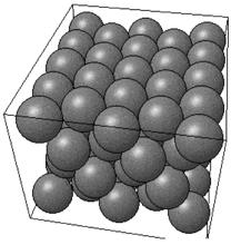
4 Important Basic Crystal Structures The three most common basic crystal structures are fcc, hcp, and bcc. first layer: hexagonally close packed fcc: face centred cubic, coordination number CN = 12 = second layer: sits in hollow sites occupied volume = 74% hcp: hexagonal close packed, CN = 12 bcc: body centred cubic, CN = 8 third layer: two possible locations hcp..abab.. "on top" fcc..abca.. "on hole" occupied volume = 74% occupied volume = 68% see Roger Nix, "An Introduction to Surface Chemistry":

 2) 3) note: hexagonal and trigonal lattices use 4 Miller indices by convention")
 = (1 0 0) Procedure: 1) Identify intercepts of plane on the x, y, and z axes.")

5 Crystal Planes Miller Indices The planes of ideal crystals (a cut through the lattice) are closely related to ideal crystal surfaces. To specifiy a particular plane most commonly Miller indices are used. 1) 2) 3) note: hexagonal and trigonal lattices use 4 Miller indices by convention (redundant)! 1 / (1,, ) = (1 0 0) Procedure: 1) Identify intercepts of plane on the x, y, and z axes. 1 x a, x b, x c (example: cubic lattice a=b=c, = = =90 ) 2) Specify intercepts in fractional coordinates of unit cell parameters a, b, c. (1 x a) / a, ( x b) / b, ( x c) / c 1,, 3) Take reciprocal of fractional intercepts, clear fractions. 1 / (1,, ) = (1 0 0) bar for negative values h k l for cubic lattice: (100), (010), (001) are identical R = (120)

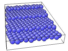
6 Simple 2D Lattices translation vectors, unit cell vectors: a, b example: Au (100) surface conventional bulk unit cell primitive surface unit cell primitive cell obeys translation symmetry see also "Wallpaper Groups: lattices":


 (100)")


7 low index surfaces: fcc (100) Ideal Crystal Surfaces bcc high index surfaces: (755) (100) (111) Pt(755) or Pt S [7(111)x(100)] (110) stepped surface (100) step 1 atom high (111) terrace 7 atoms wide (111) (10 8 7) (310) (111) compound surface: NaCl(100) Pt(10 8 7) or Pt S [7(111)x(310)] (steps with kinks)


 (2x1)")
8 Real Crystal Surfaces Reconstruction and Superlattices Relaxation: Reconstruction: Superlattices: non relaxed distance change < 10% Substantial rearrangement unit surface cell different from the bulk projected substrate relaxed driving force: unbalanced forces compared to bulk satisfying dangling bond Si(100) (2x1) bulk atom Si(111) (7x7) surface atom ( 2x 2),R45

9 Surface Defects and Structures monoatomic step terrace adatom (mobile) step adatom step vacancy (mobile) kink surface defects are important for crystal growth: traps for newly adsorbed atoms / molecules restructuring of surfaces happens at defects first kink, step, and terrace atoms have large equilibrium concentrations on real surfaces (hard to get perfect surface...) isolated adatoms and vacancies are important for atomistic transport (restructuring), but equilibrium concentration is low (< 1% of monolayer even at T melt )
 composition: adsorbing impurity atom")
 and influence crystallization speed")
10 Persistent Defects: Dislocations "dislocations": stacking faults that disrupt regularity of crystal kinetically: adsorbing species does not have enough time to find thermodynamic equilibrium (correct position) composition: adsorbing impurity atom disrupts packing point defect, missing atom, impurity: screw dislocation: propagates through crystal step dislocation, line defect: dislocations contribute to mechanical properties (ductility, brittleness) and influence crystallization speed (trapping sites)
11 Other Defect Structures mosaic: composition of "real" (imperfect) crystal of many small "ideal" (perfect) crystallites (diameter about 10 7 m) with slight misalignment of crystal axes (like rectangular bricks in an irregular wall) domain borders relate to step dislocations Frenkel Schottky defect: in ionic crystals, explains high electric conductivity in such materials Frenkel: dislocation of a single ion to an interlattice site Schottky: dislocation of single ion to crystal surface or stacking defect color center: alkali halogenide crystals > excess of metal atoms with free electrons located in the lattice > optical absorption (specific for lattice, not for metal type: K or Na)


R45 short bridge four fold hollow")
 (2x2) 2 fold hollow")
 fcc hollow (ABC.")
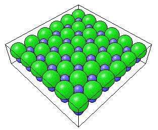
12 Surface Sites and Adsorbate Surface Structures Adsorption Sites: bridge four fold hollow Adsorbate Surface Structures: three fold hollow on top fcc (100) c(2x2) or fcc(100) ( 2x 2)R45 short bridge four fold hollow on top bridge fcc (100) p(2x2) or fcc(100) (2x2) 2 fold hollow fcc(111) ( 3x 3)R30 long bridge hcp hollow (ABA...) fcc hollow (ABC...) fcc (100) (2x1)
13 Wood s Notation and Matrix Notation Description of the ordered adlayer (adsorbed atoms and molecules) in terms of the relationship to the underlying ideal crystal plane. examples: fcc(100) alternatively: for p( 2x 2)R45
14 bulk surface Electronic and Vibronic Features of Surfaces potential energy atom spring model atom molecule 1D solid 1D solid with surface vibronic band structure electronic band structure probability density phonon wave vector: k vib = 2 vib with vib : phonon wave length, a : lattice constant electron wave vector: k = 2 with : electron wave length, a : lattice constant E pot : potential energy, E vib : vibonic energy, E el : electronic energy, E ss : energy of the surface state

 SPR (surface")

 sensor: horizontally propagating")
15 Electronic and Vibronic Features of Surfaces 2 STM image of Fe atoms on Cu(111): electronic surface states (particel in a box) SPR (surface plasmon resonance) setup: optical coupling in electronic surface states (fluorescence) SAW (surface acoustic wave) sensor: horizontally propagating acoustic surface waves
Surface Structure and Morphology 2D Crystallography
 Surface Structure and Morphology 2D Crystallography Selvage (or selvedge (it. cimosa)): Region in the solid in the vicinity of the mathematical surface Surface = Substrate (3D periodicity) + Selvage (few
Phys 412 Solid State Physics. Lecturer: Réka Albert
 Phys 412 Solid State Physics Lecturer: Réka Albert What is a solid? A material that keeps its shape Can be deformed by stress Returns to original shape if it is not strained too much Solid structure
Surface physics, Bravais lattice
 Surface physics, Bravais lattice 1. Structure of the solid surface characterized by the (Bravais) lattice + space + point group lattice describes also the symmetry of the solid material vector directions
2. Surface geometric and electronic structure: a primer
 2. Surface geometric and electronic structure: a primer 2.1 Surface crystallography 2.1.1. Crystal structures - A crystal structure is made up of two basic elements: lattice + basis Basis: Lattice: simplest
The Hamiltonian. 2.1 The Schrödinger Equation
 2 The Hamiltonian Any theoretical description has to start with the definition of the system under consideration and a determination of the fundamental interactions present in the system. This information
Crystal Structure. Dr Bindu Krishnan
 Solid State Physics-1 Crystal Structure Dr Bindu Krishnan CRYSTAL LATTICE What is crystal (space) lattice? In crystallography, only the geometrical properties of the crystal are of interest, therefore
The Solid State. Phase diagrams Crystals and symmetry Unit cells and packing Types of solid
 The Solid State Phase diagrams Crystals and symmetry Unit cells and packing Types of solid Learning objectives Apply phase diagrams to prediction of phase behaviour Describe distinguishing features of
Properties of Individual Nanoparticles
 TIGP Introduction technology (I) October 15, 2007 Properties of Individual Nanoparticles Clusters 1. Very small -- difficult to image individual nanoparticles. 2. New physical and/or chemical properties
S.No. Crystalline Solids Amorphous solids 1 Regular internal arrangement of irregular internal arrangement of particles
 Classification of solids: Crystalline and Amorphous solids: S.No. Crystalline Solids Amorphous solids 1 Regular internal arrangement of irregular internal arrangement of particles particles 2 Sharp melting
Problem with Kohn-Sham equations
 Problem with Kohn-Sham equations (So much time consuming) H s Ψ = E el Ψ ( T + V [ n] + V [ n] + V [ n]) ϕ = Eϕ i = 1, 2,.., N s e e ext XC i i N nr ( ) = ϕi i= 1 2 The one-particle Kohn-Sham equations
Chem 728 Introduction to Solid Surfaces
 Chem 728 Introduction to Solid Surfaces Solids: hard; fracture; not compressible; molecules close to each other Liquids: molecules mobile, but quite close to each other Gases: molecules very mobile; compressible
4. Interpenetrating simple cubic
 2 1. The correct structure t of CsClCl crystal is 1. Simple cubic 2. Body centered cubic 3. Face centered cubic 4. Interpenetrating simple cubic If corner as well as the particle at the center are same
Unit wise Marks Distribution of 10+2 Syllabus
 Unit wise Marks Distribution of 10+2 Syllabus S.No Unit Name Marks 1 I Solid State 4 2 II Solutions 5 3 III Electro Chemistry 5 4 IV Chemical Kinetics 5 5 V Surface Chemistry 4 6 VI General Principles
Structure and Dynamics : An Atomic View of Materials
 Structure and Dynamics : An Atomic View of Materials MARTIN T. DOVE Department ofearth Sciences University of Cambridge OXFORD UNIVERSITY PRESS Contents 1 Introduction 1 1.1 Observations 1 1.1.1 Microscopic
Chemical Bonding Ionic Bonding. Unit 1 Chapter 2
 Chemical Bonding Ionic Bonding Unit 1 Chapter 2 Valence Electrons The electrons responsible for the chemical properties of atoms are those in the outer energy level. Valence electrons - The s and p electrons
Introduction to Solid State Physics or the study of physical properties of matter in a solid phase
 Introduction to Solid State Physics or the study of physical properties of matter in a solid phase Prof. Germar Hoffmann 1. Crystal Structures 2. Reciprocal Lattice 3. Crystal Binding and Elastic Constants
Phys 460 Describing and Classifying Crystal Lattices
 Phys 460 Describing and Classifying Crystal Lattices What is a material? ^ crystalline Regular lattice of atoms Each atom has a positively charged nucleus surrounded by negative electrons Electrons are
For this activity, all of the file labels will begin with a Roman numeral IV.
 I V. S O L I D S Name Section For this activity, all of the file labels will begin with a Roman numeral IV. A. In Jmol, open the SCS file in IV.A.1. Click the Bounding Box and Axes function keys. Use the
Surface and Interface Science Physics 627; Chemistry 542. Lectures 3 Feb 1, Surface Structure
 Surface and Interface Science Physics 67; Chemistry 54 Lectures 3 Fe, 03 Surface Structure References: ) Zangwill, Pp. 8-3 ) Woodruff & Delchar, Chapter 3) Masel, Chapter 4) Ertl & Kuppers, 0-07 5) Luth,
2. Diffraction as a means to determine crystal structure
 2. Diffraction as a means to determine crystal structure Recall de Broglie matter waves: He atoms: [E (ev)] 1/2 = 0.14 / (Å) E 1Å = 0.0196 ev Neutrons: [E (ev)] 1/2 = 0.28 / (Å) E 1Å = 0.0784 ev Electrons:
The structure of liquids and glasses. The lattice and unit cell in 1D. The structure of crystalline materials. Describing condensed phase structures
 Describing condensed phase structures Describing the structure of an isolated small molecule is easy to do Just specify the bond distances and angles How do we describe the structure of a condensed phase?
Electronic Structure Theory for Periodic Systems: The Concepts. Christian Ratsch
 Electronic Structure Theory for Periodic Systems: The Concepts Christian Ratsch Institute for Pure and Applied Mathematics and Department of Mathematics, UCLA Motivation There are 10 20 atoms in 1 mm 3
UNIT I SOLID STATE PHYSICS
 UNIT I SOLID STATE PHYSICS CHAPTER 1 CRYSTAL STRUCTURE 1.1 INTRODUCTION When two atoms are brought together, two kinds of forces: attraction and repulsion come into play. The force of attraction increases
Metallic and Ionic Structures and Bonding
 Metallic and Ionic Structures and Bonding Ionic compounds are formed between elements having an electronegativity difference of about 2.0 or greater. Simple ionic compounds are characterized by high melting
2. Diffraction as a means to determine crystal structure
 Page 1 of 22 2. Diffraction as a means to determine crystal structure Recall de Broglie matter waves: 2 p h E = where p = 2m λ h 1 E = ( ) 2m λ hc E = hυ = ( photons) λ ( matter wave) He atoms: [E (ev)]
We need to be able to describe planes and directions.
 We need to be able to describe planes and directions. Miller Indices & XRD 1 2 Determining crystal structure and identifying materials (B) Plastic deformation Plastic deformation and mechanical properties
Crystallographic structure Physical vs Chemical bonding in solids
 Crystallographic structure Physical vs Chemical bonding in solids Inert gas and molecular crystals: Van der Waals forces (physics) Water and organic chemistry H bonds (physics) Quartz crystal SiO 2 : covalent
Materials for Civil and Construction Engineers CHAPTER 2. Nature of Materials
 Materials for Civil and Construction Engineers CHAPTER 2 Nature of Materials Bonds 1. Primary Bond: forms when atoms interchange or share electrons in order to fill the outer (valence) shells like noble
* motif: a single or repeated design or color
 Chapter 2. Structure A. Electronic structure vs. Geometric structure B. Clean surface vs. Adsorbate covered surface (substrate + overlayer) C. Adsorbate structure - how are the adsorbed molecules bound
PY2N20 Material Properties and Phase Diagrams
 PY2N20 Material Properties and Phase Diagrams Lecture 10 P. Stamenov, PhD School of Physics, TCD PY2N20-10 Modern CMOS pair structure Photolithographic Process CMOS Processing Steps Cu Damascene Process
Introductory Nanotechnology ~ Basic Condensed Matter Physics ~
 Introductory Nanotechnology ~ Basic Condensed Matter Physics ~ Atsufumi Hirohata Department of Electronics Go into Nano-Scale Lateral Size [m] 10-3 10-6 Micron-scale Sub-Micron-scale Nano-scale Human hair
disordered, ordered and coherent with the substrate, and ordered but incoherent with the substrate.
 5. Nomenclature of overlayer structures Thus far, we have been discussing an ideal surface, which is in effect the structure of the topmost substrate layer. The surface (selvedge) layers of the solid however
Defects in Crystals. Image borrowed from who got it from Davis & Reynolds 1996.
 Defects in Crystals Image borrowed from http://comp.uark.edu/~pjansma/geol3513_25_defmechs1_04.ppt who got it from Davis & Reynolds 1996. It's easy to think of real crystals as having these ideal structures.
CHEMISTRY. The correlation between structure and properties helps in discovering new solid materials with desired properties
 CHEMISTRY 1 The correlation between structure and properties helps in discovering new solid materials with desired properties like high temperature superconductors, magnetic materials, biodegradable polymers
1 8 =1 8 8 =1 6 =3. Unit cell Atoms at corner Atoms at faces Atoms at centre. Total no. of atoms per unit cell. bcc. fcc
 Q. No. Amorphous substances show () Short and long range order (2) Short range order (3) Long range order (4) Have no sharp M.P. Option and 3 are correct Option 2 2 and 3 are correct Option 3 3 and 4 are
THE CHEMICAL PHYSICS OF SOLID SURFACES
 THE CHEMICAL PHYSICS OF SOLID SURFACES EDITED BY D.A.KING B.Sc, Ph.D. (Rand), Sc.D. (East Anglia), F.R.S. 1920 Professor of Physical Chemistry, University of Cambridge AND D.P.WOODRUFF B.Sc. (Bristol),
Crystals Statics. Structural Properties. Geometry of lattices. Aug 23, 2018
 Crystals Statics. Structural Properties. Geometry of lattices Aug 23, 2018 Crystals Why (among all condensed phases - liquids, gases) look at crystals? We can take advantage of the translational symmetry,
Saveetha Engineering College, Thandalam, Chennai. Department of Physics. First Semester. Ph6151 Engineering Physics I (NOV/DEC 2014)
") Saveetha Engineering College, Thandalam, Chennai. Department of Physics First Semester Ph6151 Engineering Physics I (NOV/DEC 2014) Part A (Questions and Answers) 1. Distinguish between Crystalline and
Saveetha Engineering College, Thandalam, Chennai. Department of Physics First Semester Ph6151 Engineering Physics I (NOV/DEC 2014) Part A (Questions and Answers) 1. Distinguish between Crystalline and
There are 230 spacespace-groups!
 Xefg Symmetry for characteristic directions (dependent on crystal system) Non-symmorfe space groups (157 groups) Symmetry operations with translation: Screw-axis nm, 21,63, etc. Glideplane a,b,c,n,d Symmorfe
Survey of structural and electronic properties of C60 on close-packed metal surfaces
 Hong Kong Baptist University From the SelectedWorks of Professor Michel Andre Van Hove 2012 Survey of structural and electronic properties of C60 on close-packed metal surfaces Xing-Qiang Shi, Department
Chapter 1. Crystal structure. 1.1 Crystal lattices
 Chapter 1 Crystal structure 1.1 Crystal lattices We will concentrate as stated in the introduction, on perfect crystals, i.e. on arrays of atoms, where a given arrangement is repeated forming a periodic
Semiconductor physics I. The Crystal Structure of Solids
 Lecture 3 Semiconductor physics I The Crystal Structure of Solids 1 Semiconductor materials Types of solids Space lattices Atomic Bonding Imperfection and doping in SOLIDS 2 Semiconductor Semiconductors
Chapter 2. Atomic Packing
 Chapter 2. Atomic Packing Contents 2-1. Packing of directional bonding atoms 2-2. Packing of indirectional bonding in same size atoms 2-3. Packing of indirectional bonding in different size atoms 2-4.
Supplementary Figures
 Supplementary Figures Supplementary Figure 1: Region mapping. a Pristine and b Mn-doped Bi 2 Te 3. Arrows point at characteristic defects present on the pristine surface which have been used as markers
Atomic Arrangement. Primer Materials For Science Teaching Spring
 Atomic Arrangement Primer Materials For Science Teaching Spring 2016 31.3.2015 Levels of atomic arrangements No order In gases, for example the atoms have no order, they are randomly distributed filling
Atomic Arrangement. Primer in Materials Spring
 Atomic Arrangement Primer in Materials Spring 2017 30.4.2017 1 Levels of atomic arrangements No order In gases, for example the atoms have no order, they are randomly distributed filling the volume to
Introduction to Crystal Structure and Bonding. Prof.P. Ravindran, Department of Physics, Central University of Tamil Nadu, India
 Introduction to Crystal Structure and Bonding 1 Prof.P. Ravindran, Department of Physics, Central University of Tamil Nadu, India http://folk.uio.no/ravi/semi2013 Fundamental Properties of matter 2 Matter:
PH575 Spring Lecture #19 Semiconductors: electrical & optical properties: Kittel Ch. 8 pp ; Ch. 20
 PH575 Spring 2014 Lecture #19 Semiconductors: electrical & optical properties: Kittel Ch. 8 pp. 205-214; Ch. 20 Simplified diagram of the filling of electronic band structure in various types of material,
Properties of Liquids and Solids. Vaporization of Liquids. Vaporization of Liquids. Aims:
 Properties of Liquids and Solids Petrucci, Harwood and Herring: Chapter 13 Aims: To use the ideas of intermolecular forces to: Explain the properties of liquids using intermolecular forces Understand the
Properties of Liquids and Solids. Vaporization of Liquids
 Properties of Liquids and Solids Petrucci, Harwood and Herring: Chapter 13 Aims: To use the ideas of intermolecular forces to: Explain the properties of liquids using intermolecular forces Understand the
Crystallographic Symmetry. Jeremy Karl Cockcroft
 Crystallographic Symmetry Jeremy Karl Cockcroft Why bother? To describe crystal structures Simplifies the description, e.g. NaCl structure Requires coordinates for just 2 atoms + space group symmetry!
FIRST MIDTERM EXAM Chemistry March 2011 Professor Buhro
 FIRST MIDTERM EXAM Chemistry 465 1 March 2011 Professor Buhro Signature Print Name Clearly ID Number: Information. This is a closed-book exam; no books, notes, other students, other student exams, or any
2) Atom manipulation. Xe / Ni(110) Model: Experiment:
 Atom manipulation. Xe / Ni(110) Model: Experiment:") 2) Atom manipulation D. Eigler & E. Schweizer, Nature 344, 524 (1990) Xe / Ni(110) Model: Experiment: G.Meyer, et al. Applied Physics A 68, 125 (1999) First the tip is approached close to the adsorbate
2) Atom manipulation D. Eigler & E. Schweizer, Nature 344, 524 (1990) Xe / Ni(110) Model: Experiment: G.Meyer, et al. Applied Physics A 68, 125 (1999) First the tip is approached close to the adsorbate
Lecture Note on Crystal structures Masatsugu Sei Suzuki and Itsuko S. Suzuki Department of Physics, SUNY at Binghamton (Date: February 03, 2012)
") Lecture Note on Crystal structures Masatsugu Sei Suzuki and Itsuko S. Suzuki Department of Physics, SUNY at Binghamton (Date: February 03, 2012) This is a part of lecture note on solid state physics (Phys.472/572)
Lecture Note on Crystal structures Masatsugu Sei Suzuki and Itsuko S. Suzuki Department of Physics, SUNY at Binghamton (Date: February 03, 2012) This is a part of lecture note on solid state physics (Phys.472/572)
CRYSTAL STRUCTURES WITH CUBIC UNIT CELLS
 CRYSTAL STRUCTURES WITH CUBIC UNIT CELLS Crystalline solids are a three dimensional collection of individual atoms, ions, or whole molecules organized in repeating patterns. These atoms, ions, or molecules
Introduction to Solid State
 http://en.wikipedia.org/wiki/bravais_lattice Introduction to Solid State Crystalline vs. non-crystalline solids: Lattice Unit cell No. of spheres in a unit cell : Bravais lattices In geometry and crystallography,
MP464: Solid State Physics Problem Sheet
 MP464: Solid State Physics Problem Sheet 1) Write down primitive lattice vectors for the -dimensional rectangular lattice, with sides a and b in the x and y-directions respectively, and a face-centred
INTRODUCTION TO THE DEFECT STATE IN MATERIALS
 INTRODUCTION TO THE DEFECT STATE IN MATERIALS DEFECTS, DEFECTS, DEFECTS CAN T LIVE WITH THEM!!! CAN T LIVE WITHOUT THEM!!! INTRODUCTION TO DEFECT STATE IN MATERIALS DEFECTS, DEFECTS, DEFECTS Perfect crystals
Ionic Bonding. Chem
 Whereas the term covalent implies sharing of electrons between atoms, the term ionic indicates that electrons are taken from one atom by another. The nature of ionic bonding is very different than that
SOLID STATE MODULE - 3. Objectives. Solid State. States of matter. Notes
 Solid State MODULE - 3 8 SOLID STATE Y ou are aware that the matter exists in three different states viz., solid, liquid and gas. In these, the constituent particles (atoms, molecules or ions) are held
Class XII Chapter 1 The Solid State Chemistry. Define the term amorphous give a few examples of amorphous solids.
 Book Name: NCERT Solution Question 1: Define the term amorphous give a few examples of amorphous solids. Solution 1: Amorphous solids are the solids whose constituent particles are of irregular shapes
Ram Seshadri MRL 2031, x6129, These notes complement chapter 6 of Anderson, Leaver, Leevers and Rawlings
 Crystals, packings etc. Ram Seshadri MRL 2031, x6129, seshadri@mrl.ucsb.edu These notes complement chapter 6 of Anderson, Leaver, Leevers and Rawlings The unit cell and its propagation Materials usually
5. Defects Thermal defects Planar defects Linear defects Point defects stochiometric compounds Schottky defects Anti-Schottky defects
 5. Defects According to the third law of thermodynamics, only in 0[K] crystal's entropy can reach its minimum. As a consequence, if the temperature is higher than 0[K] there must be imperfections in the
Nearly Free Electron Gas model - I
 Nearly Free Electron Gas model - I Contents 1 Free electron gas model summary 1 2 Electron effective mass 3 2.1 FEG model for sodium...................... 4 3 Nearly free electron model 5 3.1 Primitive
1.4 Crystal structure
 1.4 Crystal structure (a) crystalline vs. (b) amorphous configurations short and long range order only short range order Abbildungen: S. Hunklinger, Festkörperphysik, Oldenbourg Verlag represenatives of
Defects. Defects. Kap. 3 States of aggregation. Perfect Crystal
 Kap. 3 States of aggregation Defects Perfect Crystal A A perfect crystal with every atom in the correct position does not exist. Only a hypothetical situation at 0 K Crystals are like people: it is the
Lecture 6 - Bonding in Crystals
 Lecture 6 onding in Crystals inding in Crystals (Kittel Ch. 3) inding of atoms to form crystals A crystal is a repeated array of atoms Why do they form? What are characteristic bonding mechanisms? How
Lecture 2: Bonding in solids
 Lecture 2: Bonding in solids Electronegativity Van Arkel-Ketalaar Triangles Atomic and ionic radii Band theory of solids Molecules vs. solids Band structures Analysis of chemical bonds in Reciprocal space
VERY SHORT ANSWER TYPE QUESTIONS (1 Mark)
") UNIT I 10 Chemistry-XII THE SOLID STATE VERY SHORT ANSWER TYPE QUESTIONS (1 Mark) Q. 1. What do you mean by paramagnetic substance? Ans. Weakly attracted by magnetic eld and these substances are made of
UNIT I 10 Chemistry-XII THE SOLID STATE VERY SHORT ANSWER TYPE QUESTIONS (1 Mark) Q. 1. What do you mean by paramagnetic substance? Ans. Weakly attracted by magnetic eld and these substances are made of
X-ray, Neutron and e-beam scattering
 X-ray, Neutron and e-beam scattering Introduction Why scattering? Diffraction basics Neutrons and x-rays Techniques Direct and reciprocal space Single crystals Powders CaFe 2 As 2 an example What is the
ME 254 MATERIALS ENGINEERING 1 st Semester 1430/ st Med-Term Exam (1.5 hrs)
") ME 254 MATERIALS ENGINEERING 1 st Semester 1430/1431 1 st Med-Term Exam (1.5 hrs) قسم الهندسة الميكانيكية Question 1 a) Classify the materials based on their properties and performance, give some examples.
ME 254 MATERIALS ENGINEERING 1 st Semester 1430/1431 1 st Med-Term Exam (1.5 hrs) قسم الهندسة الميكانيكية Question 1 a) Classify the materials based on their properties and performance, give some examples.
Solids. properties & structure
 Solids properties & structure Determining Crystal Structure crystalline solids have a very regular geometric arrangement of their particles the arrangement of the particles and distances between them is
Diamond. There are four types of solid: -Hard Structure - Tetrahedral atomic arrangement. What hybrid state do you think the carbon has?
 Bonding in Solids Bonding in Solids There are four types of solid: 1. Molecular (formed from molecules) - usually soft with low melting points and poor conductivity. 2. Covalent network - very hard with
Physical Chemistry I. Crystal Structure
 Physical Chemistry I Crystal Structure Crystal Structure Introduction Crystal Lattice Bravis Lattices Crytal Planes, Miller indices Distances between planes Diffraction patters Bragg s law X-ray radiation
MODERN PUBLISHERS (Producers of Quality Text & Competition Books)
") MODERN PUBLISHERS (Producers of Quality Text & Competition Books) UR ADDRESSES IN INDIA MBD PRINTOGRAPHICS (P) LTD. Ram Nagar, Industrial Area, Gagret, Distt. Una (H.P.) and...write to save nature we
MODERN PUBLISHERS (Producers of Quality Text & Competition Books) UR ADDRESSES IN INDIA MBD PRINTOGRAPHICS (P) LTD. Ram Nagar, Industrial Area, Gagret, Distt. Una (H.P.) and...write to save nature we
Inorganic Chemistry I (CH331) Solid-state Chemistry I (Crystal structure) Nattapol Laorodphan (Chulabhorn Building, 4 th Floor)
 Solid-state Chemistry I (Crystal structure) Nattapol Laorodphan (Chulabhorn Building, 4 th Floor)") Inorganic Chemistry I (CH331) Solid-state Chemistry I (Crystal structure) Nattapol Laorodphan (Chulabhorn Building, 4 th Floor) 7/2013 N.Laorodphan 1 Text books : 1. D.F. Sheiver, P.W. Atkins & C.H. Langford
Inorganic Chemistry I (CH331) Solid-state Chemistry I (Crystal structure) Nattapol Laorodphan (Chulabhorn Building, 4 th Floor) 7/2013 N.Laorodphan 1 Text books : 1. D.F. Sheiver, P.W. Atkins & C.H. Langford
Structures of Solids. Unit Cells - Not(?) Chapter 4 Ionic and Other Inorganic Solids. CHEM 462 Wednesday, September 22 T.
 Chapter 4 Ionic and Other Inorganic Solids. CHEM 462 Wednesday, September 22 T.") Chapter 4 Ionic and Other Inorganic Solids CHEM 462 Wednesday, September 22 T. Hughbanks Structures of Solids Many dense solids are described in terms of packing of atoms or ions. Although these geometric
Chapter 4 Ionic and Other Inorganic Solids CHEM 462 Wednesday, September 22 T. Hughbanks Structures of Solids Many dense solids are described in terms of packing of atoms or ions. Although these geometric
There are four types of solid:
 Bonding in Solids There are four types of solid: 1. Molecular (formed from molecules) - usually soft with low melting points and poor conductivity. 2. Covalent network - very hard with very high melting
PART 1 Introduction to Theory of Solids
 Elsevier UK Job code: MIOC Ch01-I044647 9-3-2007 3:03p.m. Page:1 Trim:165 240MM TS: Integra, India PART 1 Introduction to Theory of Solids Elsevier UK Job code: MIOC Ch01-I044647 9-3-2007 3:03p.m. Page:2
Earth Materials Lab 2 - Lattices and the Unit Cell
 Earth Materials Lab 2 - Lattices and the Unit Cell Unit Cell Minerals are crystallographic solids and therefore are made of atoms arranged into lattices. The average size hand specimen is made of more
Solid State. Subtopics
 01 Solid State Chapter 01: Solid State Subtopics 1.0 Introduction 1.1 Classification of solids 1.2 Classification of crystalline solids 1.3 Unit cell, two and three dimensional lattices and number of atoms
ECE 474: Principles of Electronic Devices. Prof. Virginia Ayres Electrical & Computer Engineering Michigan State University
 ECE 474: Principles of Electronic Devices Prof. Virginia Ayres Electrical & Computer Engineering Michigan State University ayresv@msu.edu Lecture 06: Completed: Chapter 01: quantify physical structures
Self-Assembled Monolayers
 Self-Assembled Monolayers Literature and Further Information Surface Chemistry: www.chem.qmul.ac.uk/surfaces/scc/ www.nottingham.ac.uk/~ppzpjm/amshome.htm venables.asu.edu/grad/lectures.html SAM s: www.ifm.liu.se/applphys/ftir/sams.html
Structure of Surfaces
 Structure of Surfaces C Stepped surface Interference of two waves Bragg s law Path difference = AB+BC =2dsin ( =glancing angle) If, n =2dsin, constructive interference Ex) in a cubic lattice of unit cell
1/2, 1/2,1/2, is the center of a cube. Induces of lattice directions and crystal planes (a) Directions in a crystal Directions in a crystal are
 Directions in a crystal Directions in a crystal are") Crystallography Many materials in nature occur as crystals. Examples include the metallic elements gold, copper and silver, ionic compounds such as salt (e.s. NaCl); ceramics, rutile TiO2; and nonmetallic
Crystallography Many materials in nature occur as crystals. Examples include the metallic elements gold, copper and silver, ionic compounds such as salt (e.s. NaCl); ceramics, rutile TiO2; and nonmetallic
Bravais Lattice + Basis = Crystal Structure
 Bravais Lattice + Basis = Crystal Structure A crystal structure is obtained when identical copies of a basis are located at all of the points of a Bravais lattice. Consider the structure of Cr, a I-cubic
DIFFRACTION PHYSICS THIRD REVISED EDITION JOHN M. COWLEY. Regents' Professor enzeritus Arizona State University
 DIFFRACTION PHYSICS THIRD REVISED EDITION JOHN M. COWLEY Regents' Professor enzeritus Arizona State University 1995 ELSEVIER Amsterdam Lausanne New York Oxford Shannon Tokyo CONTENTS Preface to the first
1 Crystal Structures. of three-dimensional crystals. Here we use two-dimensional examples to illustrate the concepts.
 3 1 Crystal Structures A crystal is a periodic array of atoms. Many elements and quite a few compounds are crystalline at low enough temperatures, and many of the solid materials in our everyday life (like
Crystallography Reading: Warren, Chapters 2.1, 2.2, 2.6, 8 Surface symmetry: Can be a clue to underlying structure. Examples:
 Crystallography Reading: Warren, Chapters 2.1, 2.2, 2.6, 8 Surface symmetry: Can be a clue to underlying structure. Examples: Snow (SnowCrystals.com) Bismuth (Bao, Kavanagh, APL 98 66103 (2005) Hexagonal,
Concepts in Surface Physics
 M.-C. Desjonqueres D. Spanjaard Concepts in Surface Physics Second Edition With 257 Figures Springer 1. Introduction................................. 1 2. Thermodynamical and Statistical Properties of
Class XII Chapter 1 The Solid State Chemistry
 Question 1.1: Define the term 'amorphous'. Give a few examples of amorphous solids. Amorphous solids are the solids whose constituent particles are of irregular shapes and have short range order. These
Inorganic Exam 1 Chm October 2010
 Inorganic Exam 1 Chm 451 28 October 2010 Name: Instructions. Always show your work where required for full credit. 1. In the molecule CO 2, the first step in the construction of the MO diagram was to consider
Classification of Solids, Fermi Level and Conductivity in Metals Dr. Anurag Srivastava
 Classification of Solids, Fermi Level and Conductivity in Metals Dr. Anurag Srivastava Web address: http://tiiciiitm.com/profanurag Email: profanurag@gmail.com Visit me: Room-110, Block-E, IIITM Campus
Scanning Tunneling Microscopy. how does STM work? the quantum mechanical picture example of images how can we understand what we see?
 Scanning Tunneling Microscopy how does STM work? the quantum mechanical picture example of images how can we understand what we see? Observation of adatom diffusion with a field ion microscope Scanning
PRINCIPLES OF ADSORPTION AND REACTION ON SOLID SURFACES
 PRINCIPLES OF ADSORPTION AND REACTION ON SOLID SURFACES Richard I. Masel Department of Chemical Engineering University of Illinois at Urbana-Champaign Urbana, Illinois A WILEY-INTERSCIENCE PUBLICATION
3-D Crystal Lattice Images
 3-D Crystal Lattice Images All of the following images are crossed-stereo pairs. To view them, cross your eyes and focus. Author's note this material has been expanded and updated, and can be found at
Physics 211B : Problem Set #0
 Physics 211B : Problem Set #0 These problems provide a cross section of the sort of exercises I would have assigned had I taught 211A. Please take a look at all the problems, and turn in problems 1, 4,
Crystal Models. Figure 1.1 Section of a three-dimensional lattice.
 Crystal Models The Solid-State Structure of Metals and Ionic Compounds Objectives Understand the concept of the unit cell in crystalline solids. Construct models of unit cells for several metallic and
HW# 5 CHEM 281 Louisiana Tech University, POGIL(Process Oriented Guided Inquiry Learning) Exercise on Chapter 3. Structures of Ionic Solids. Why?
 Exercise on Chapter 3. Structures of Ionic Solids. Why?") HW# 5 CHEM 281 Louisiana Tech University, POGIL(Process Oriented Guided Inquiry Learning) Exercise on Chapter 3. Structures of Ionic Solids. Why? Many ionic structures may be described as close-packed
HW# 5 CHEM 281 Louisiana Tech University, POGIL(Process Oriented Guided Inquiry Learning) Exercise on Chapter 3. Structures of Ionic Solids. Why? Many ionic structures may be described as close-packed
STM spectroscopy (STS)
") STM spectroscopy (STS) di dv 4 e ( E ev, r) ( E ) M S F T F Basic concepts of STS. With the feedback circuit open the variation of the tunneling current due to the application of a small oscillating voltage
STM spectroscopy (STS) di dv 4 e ( E ev, r) ( E ) M S F T F Basic concepts of STS. With the feedback circuit open the variation of the tunneling current due to the application of a small oscillating voltage