The importance of the momentum flux on the mechanical properties of sputter deposited TiN thin films.
|
|
|
- Hubert Edwards
- 5 years ago
- Views:
Transcription
1 The importance of the momentum flux on the mechanical properties of sputter deposited TiN thin films. S. Mahieu and D. Depla Ghent University Partially Funded by the FWO-Flanders
2 P.H. Mayrhofer et al. TSF () 89 H. Wang et al. TSF 51 (8) 519 J. Musil et al. Surf. Coat. Techn () 89 Ion energy E i Ion-to-atom ratio i/a Ion energy flux E i x i/a Mechanical properties related to energy and flux of ions.
3 Increasing the ion energy or ion flux also influences momentum flux. Ar Ti e - Ar +- Ti target N d T-S E sp Ar E refl + Ar E ion How to quantify the momentum flux? Substrate
4 Ti target Ar Ti e - N Ar +- d T-S E sp Ar E refl + Ar E ion Substrate A: Quantify separate contribution 1 of - ions - sputtered particles - reflected neutrals B: Develop a tool to measure total momentum flux 1: S. Mahieu, D. Depla: J.Appl. Phys. 1 (8) 111 : UK patent application number GB9917. monitoring tool for deposition processes S. Mahieu, D. Depla
5 : ions Energy distribution and flux of ions: RFEA Mass distribution: energy resolved mass spectrometry 5 M ion = i m a m i i a i E ion : average mass of ions : ion-to-atom ratio (i from RFEA, a from SiMTRA 1 ) E ion : average energy of ions 1: K. Van Aeken, S. Mahieu, D. Depla: J. Phys. D: Appl. Phys 1 (8) 57 Free download:
6 : sputtered particles Energy distribution and flux: SiMTRA 1 Mass distribution: energy resolved mass spectrometry sp fraction of Ti/TiN adatoms ( f M f M ) M = + Ti Ti TiN 1: K. Van Aeken, S. Mahieu, D. Depla: J. Phys. D: Appl. Phys 1 (8) 57 Free download: TiN M = me sp average energy sputtered particles
7 : reflected neutrals Flux, energy and mass distribution: SiMTRA + SRIM 1 7 M refl Ar refl, Ar N refl, N = f, + refl, N Ar mar E refl Ar f N mn E YAr Fsp, Ar YN Fsp, N B F Backscatter yield Gas composition Average energy Sputter yield 1: Stopping Range of in Matter B F Transportation coefficients
8 : flux monitor Rotatable wire holder Torsion wire Front plate Front view Opening area A d Back view b 8 Fd = kθ period T and = π F I = pφa k => with Mb I = 1 momentum π Mb θ flux : P = pφ = dt A UK patent application number GB9917. monitoring tool for deposition processes S. Mahieu, D. Depla


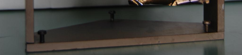
9 : flux monitor Torsion wire Opening area A Torsion plate reflector Front view 9 Back view UK patent application number GB9917. monitoring tool for deposition processes S. Mahieu, D. Depla
10 Ti target Ar Ti e - N Ar +- d T-S E sp Ar E refl + Ar E ion Substrate 1 A: Quantify separate contribution 1 of - ions - sputtered particles - reflected neutrals B: Develop a tool to measure total momentum flux 1: S. Mahieu, D. Depla: J.Appl. Phys. 1 (8) 111 : UK patent application number GB9917. monitoring tool for deposition processes S. Mahieu, D. Depla
11 8x1-1 x1 - factor 5 calculated M tot measured calculated 1 Measured M tot 9 1 N flow (sccm) Momentum/metallic flux increases with - increasing N flow
12 1x1-1 1 calculated M tot 1 8 calculated measured 5x1-1 Measured M tot factor target-substrate distance (cm) 1 Momentum/metallic flux increases with - increasing N flow - decreasing T-S distance 8x1-1 calculated M tot 9 measured 1 N flow (sccm) calculated 1 18 x1 - Measured M tot
13 1 x1-1 calculated M tot. calculated.5 measured pressure (Pa) Momentum/metallic flux increases with - increasing N flow - decreasing T-S distance - decreasing pressure.7 Factor 5 due to callibration RFEA.9 5x1-1 Measured M tot 1x1-1 calculated M tot (kgm /s) 1 1 8x1-1 calculated M tot 8 7 factor 5 measured calculated target-substrate distance (cm) measured calculated 9 1 N flow (sccm) x1 - M easured M tot x1 - Measured M tot
14 Hardness (GPa) Mechanical properties versus measured momentum flux x1-1 1 Measured M tot Measured M tot 1 x1-1 Elastic Modulus (GPa) 1 If Kendall tau rank correlation coefficient >.58 significant correlation 1 : Z =. Z =. Statistical relation between mechanical properties and momentum flux 1: H. Abdi, in Encyclopedia of Measurement and Statistics, edited by N.J. Salkind (SAGE, New Delhi, 7), p.58
15 Mechanical properties versus ion energy Hardness (GPa) ion energy E i (ev) ion energy E i (ev) Elastic modulus (GPa) Z = 1.9 Z = 1.7 <.58 No statistical relation between mechanical properties and ion energy
16 Hardness (GPa) Mechanical properties versus ion-to-atom ratio ion-to-atom ratio I ion-to-atom ratio I Elastic modulus (GPa) 1 Z = 1.7 Z =. <.58 No statistical relation between mechanical properties and ion-to-atom ratio
 calculated M tot 1 1 8 7 1 9 measured calculated 9 11 1")
 Measured and calculated values correspond Mechanical properties related")
17 M = M + M + tot ion sp M refl can be calculated Torsion wire can be measured reflector Torsion plate 1x1-1 5x1-17 Hardness (GPa) calculated M tot measured calculated target-substrate distance (cm) 1 Measured M tot 1 x1-1 Measured M tot (kgm /s) 1 Measured M tot 1 x1-1 Elastic Modulus (GPa) Measured and calculated values correspond Mechanical properties related to momentum flux
18 THANK YOU 18 Thanks to: -IWT Flanders and FWO Flanders for financial support Download SiMTRA from
Some more equations describing reactive magnetron sputtering.
 Some more equations describing reactive magnetron sputtering D. Depla, S. Mahieu, W. Leroy, K. Van Aeken, J. Haemers, R. De Gryse www.draft.ugent.be discharge voltage (V) 44 4 36 32 28..5 1. 1.5 S (Pumping
Simulation of Metal TRAnport. SIMTRA : a tool to predict and understand deposition. K. Van Aeken, S. Mahieu, D. Depla.
 Simulation of Metal TRAnport SIMTRA : a tool to predict and understand deposition K. Van Aeken, S. Mahieu, D. Depla www.draft.ugent.be 1) : Why do we calculate? ) Scientific background : How do we calculate?
In search for the limits of
 In search for the limits of rotating cylindrical magnetron sputtering W. P. Leroy, S. Mahieu, R. De Gryse, D. Depla DRAFT Dept. Solid State Sciences Ghent University Belgium www.draft.ugent.be Planar Magnetron
Towards quantitative modelling of magnetron sputter deposition
 Towards quantitative modelling of magnetron sputter deposition D. Depla Dedicated Research on Advanced Films and Targets Ghent University Magnetron sputtering: components A magnetron discharge is a magnetically
Reactive magnetron sputter deposition: a journey from target to substrate
 Reactive magnetron sputter deposition: a journey from target to substrate D. Depla Dedicated Research on Advanced Films and Targets Ghent University Setting the scene Who? Some keywords Main features of
Energy fluxes in plasmas for fabrication of nanostructured materials
 Energy fluxes in plasmas for fabrication of nanostructured materials IEAP, Universität Kiel 2nd Graduate Summer Institute "Complex Plasmas" August 5-13, 2010 in Greifswald (Germany) AG 1 Outline Motivation
Modelling of the Target Voltage Behaviour in Reactive Sputtering R. De Gryse*, D. Depla University Ghent, Krijgslaan 281/S1, B-9000 GENT, Belgium
 Modelling of the Target Voltage Behaviour in Reactive Sputtering R. De Gryse*, D. Depla University Ghent, Krijgslaan 28/S, B-9 GENT, Belgium Abstract It has been shown that at least two mechanisms are
This is an author produced version of a paper presented at 2nd PATCMC, June 6th-8th 2011 Plzeň, Czech Republic.
 http://uu.diva-portal.org This is an author produced version of a paper presented at 2nd PATCMC, June 6th-8th 2011 Plzeň, Czech Republic. Kubart, T. 2011. Process modelling for reactive magnetron sputtering
Impact of Chamber Pressure on Sputtered Particle Energy
 Wilmert De Bosscher Chief Technology Officer +32 9381 6177 wilmert.debosscher@soleras.com Impact of Chamber Pressure on Sputtered Particle Energy Tampa, October 18 th, 2017 Background Why Sputtering at
Effects of Energy-Assistance on Coating Microstructure
 4 th Vacuum Symposium 16 th October 2013 Effects of Energy-Assistance on Coating Microstructure JOHN S COLLIGON Dalton Research Institute Manchester Metropolitan University Manchester M15GD, UK email:
Hysteresis-free reactive high power impulse magnetron sputtering
 Linköping University Postprint Hysteresis-free reactive high power impulse magnetron sputtering E. Wallin and U. Helmersson N.B.: When citing this work, cite the original article. Original publication:
ECE Semiconductor Device and Material Characterization
 ECE 4813 Semiconductor Device and Material Characterization Dr. Alan Doolittle School of Electrical and Computer Engineering Georgia Institute of Technology As with all of these lecture slides, I am indebted
Contents. Bibliografische Informationen digitalisiert durch
 1 Simulation of the Sputtering Process T. Ono, T. Kenmotsu, and T. Muramoto 1 1.1 Introduction 1 1.2 Computer Simulation Codes 2 1.3 Total Sputtering Yield 5 1.3.1 Incident-Energy Dependence of Sputtering
Sputter rate distribution and compositional variations in films sputtered from elemental and multi-element targets at different pressures
 International Journal of Materials Science and Applications 014; 3(): 9-36 Published online February 8, 014 (http://www.sciencepublishinggroup.com/j/ijmsa) doi: 10.11648/j.ijmsa.014030.14 Sputter rate
Section 5: Thin Film Deposition part 1 : sputtering and evaporation. Jaeger Chapter 6. EE143 Ali Javey
 Section 5: Thin Film Deposition part 1 : sputtering and evaporation Jaeger Chapter 6 Vacuum Basics 1. Units 1 atmosphere = 760 torr = 1.013x10 5 Pa 1 bar = 10 5 Pa = 750 torr 1 torr = 1 mm Hg 1 mtorr =
Application of Rarefied Flow & Plasma Simulation Software
 2016/5/18 Application of Rarefied Flow & Plasma Simulation Software Yokohama City in Japan Profile of Wave Front Co., Ltd. Name : Wave Front Co., Ltd. Incorporation : March 1990 Head Office : Yokohama
Quasi-periodic nanostructures grown by oblique angle deposition
 JOURNAL OF APPLIED PHYSICS VOLUME 94, NUMBER 12 15 DECEMBER 2003 Quasi-periodic nanostructures grown by oblique angle deposition T. Karabacak, a) G.-C. Wang, and T.-M. Lu Department of Physics, Applied
June 5, 2012: Did you miss it? No Problem. Next chance in Venus in Front of the Sun and there is more: plasma imaging!
 July 18 20, 2012 5th Int. Workshop on "Thin Films Applied To Superconducting RF And New Ideas For Pushing The Limits Of RF Superconductivity" Jefferson Lab, VA Strong localization of ionization in high
Increased ionization during magnetron sputtering and its influence on the energy balance at the substrate
 Institute of Experimental and Applied Physics XXII. Erfahrungsaustausch Oberflächentechnologie mit Plasma- und Ionenstrahlprozessen Mühlleithen, 10.-12. März, 2015 Increased ionization during magnetron
The Effect of Deposition Parameter on Electrical Resistivity of TiAlN Thin Film
 HWAHAK KONGHAK Vol. 40, No. 4, August, 00, pp. 59-533 TiAlN Electrical Resistivity * * (00 4 3, 00 7 31 ) The Effect of Deposition Parameter on Electrical Resistivity of TiAlN Thin Film Young Soo Song,
 http://www.diva-portal.org This is the published version of a paper presented at Invited talk: 12th International Symposium on Sputtering and Plasma Processes, Kyoto, July 10-12, 2013. Citation for the
CLUSTER SIZE DEPENDENCE OF SPUTTERING YIELD BY CLUSTER ION BEAM IRRADIATION
 CLUSTER SIZE DEPENDENCE OF SPUTTERING YIELD BY CLUSTER ION BEAM IRRADIATION T. Seki 1,2), T. Murase 1), J. Matsuo 1) 1) Quantum Science and Engineering Center, Kyoto University 2) Collaborative Research
Analyses of LiNbO 3 wafer surface etched by ECR plasma of CHF 3 & CF 4
 1998 DRY PROCESS SYMPOSIUM VI - 3 Analyses of LiNbO 3 wafer surface etched by ECR plasma of CHF 3 & CF 4 Naoki Mitsugi, Kaori Shima, Masumi Ishizuka and Hirotoshi Nagata New Technology Research Laboratories,
ECE 695 Numerical Simulations Lecture 35: Solar Hybrid Energy Conversion Systems. Prof. Peter Bermel April 12, 2017
 ECE 695 Numerical Simulations Lecture 35: Solar Hybrid Energy Conversion Systems Prof. Peter Bermel April 12, 2017 Ideal Selective Solar Absorber Efficiency Limits Ideal cut-off wavelength for a selective
Lecture 22 Ion Beam Techniques
 Lecture 22 Ion Beam Techniques Schroder: Chapter 11.3 1/44 Announcements Homework 6/6: Will be online on later today. Due Wednesday June 6th at 10:00am. I will return it at the final exam (14 th June).
Desorption and Sputtering on Solid Surfaces by Low-energy Multicharged Ions
 Desorption and Sputtering on Solid Surfaces by Low-energy Multicharged Ions K. Motohashi Department of Biomedical Engineering, Toyo University motohashi@toyonet.toyo.ac.jp 1. Background Sputtering and
Reactive magnetron sputtering deposition and columnar growth of nc-tic/a-c Galvan, D.; Pei, Yutao T.; De Hosson, J.T.M.
 University of Groningen Reactive magnetron sputtering deposition and columnar growth of nc-tic/a-c Galvan, D.; Pei, Yutao T.; De Hosson, J.T.M. Published in: Journal of Vacuum Science & Technology A DOI:
Plasma diagnostics of pulsed sputtering discharge
 Plasma diagnostics of pulsed sputtering discharge Vitezslav Stranak Zdenek Hubicka, Martin Cada and Rainer Hippler University of Greifswald, Institute of Physics, Felix-Hausdorff-Str. 6, 174 89 Greifswald,
Multilayer coating facility for the HEFT hard X-ray telescope
 Multilayer coating facility for the HEFT hard X-ray telescope Carsten P. Jensen a, Finn E. Christensen a, Hubert Chen b, Erik B. W.Smitt a, Eric Ziegler c a Danish Space Research Institute (Denmark); b
DEPOSITION OF THIN TiO 2 FILMS BY DC MAGNETRON SPUTTERING METHOD
 Chapter 4 DEPOSITION OF THIN TiO 2 FILMS BY DC MAGNETRON SPUTTERING METHOD 4.1 INTRODUCTION Sputter deposition process is another old technique being used in modern semiconductor industries. Sputtering
Transparent Electrode Applications
 Transparent Electrode Applications LCD Solar Cells Touch Screen Indium Tin Oxide (ITO) Zinc Oxide (ZnO) - High conductivity - High transparency - Resistant to environmental effects - Rare material (Indium)
Surface analysis techniques
 Experimental methods in physics Surface analysis techniques 3. Ion probes Elemental and molecular analysis Jean-Marc Bonard Academic year 10-11 3. Elemental and molecular analysis 3.1.!Secondary ion mass
Global modeling of HiPIMS systems: transition from homogeneous to self organized discharges
 RUHR-UNIVERSITÄT BOCHUM Global modeling of HiPIMS systems: transition from homogeneous to self organized discharges S. Gallian 1, J. Trieschmann 1, T. Mussenbrock 1, W. N. G. Hitchon 2 and R. P. Brinkmann
6.5 Optical-Coating-Deposition Technologies
 92 Chapter 6 6.5 Optical-Coating-Deposition Technologies The coating process takes place in an evaporation chamber with a fully controlled system for the specified requirements. Typical systems are depicted
Measurement of Absolute Argon Excited State Populations and Electron Energy Distribution Functions in an Ar-a-Si Plasma
 University of Arkansas, Fayetteville ScholarWorks@UARK Electrical Engineering Undergraduate Honors Theses Electrical Engineering 5-2008 Measurement of Absolute Argon Excited State Populations and Electron
Combinatorial RF Magnetron Sputtering for Rapid Materials Discovery: Methodology and Applications
 Combinatorial RF Magnetron Sputtering for Rapid Materials Discovery: Methodology and Applications Philip D. Rack,, Jason D. Fowlkes,, and Yuepeng Deng Department of Materials Science and Engineering University
Investigation of tungsten incorporated amorphous carbon lm
 Thin Solid Films 355±356 (1999) 174±178 www.elsevier.com/locate/tsf Investigation of tungsten incorporated amorphous carbon lm Rusli a, *, S.F. Yoon a, H. Yang a, J. Ahn a, Q.F. Huang a, Q. Zhang a, Y.P.
The Benefit of Wide Energy Range Spectrum Acquisition During Sputter Depth Profile Measurements
 The Benefit of Wide Energy Range Spectrum Acquisition During Sputter Depth Profile Measurements Uwe Scheithauer, 82008 Unterhaching, Germany E-Mail: scht.uhg@googlemail.com Internet: orcid.org/0000-0002-4776-0678;
SUPPLEMENTARY INFORMATION
 Engineered doping of organic semiconductors for enhanced thermoelectric efficiency G.-H. Kim, 1 L. Shao, 1 K. Zhang, 1 and K. P. Pipe 1,2,* 1 Department of Mechanical Engineering, University of Michigan,
High Resolution Photoemission Study of the Spin-Dependent Band Structure of Permalloy and Ni
 High Resolution Photoemission Study of the Spin-Dependent Band Structure of Permalloy and Ni K. N. Altmann, D. Y. Petrovykh, and F. J. Himpsel Department of Physics, University of Wisconsin, Madison, 1150
RGA modelling and simulation to include pressure dependence in the ion source
 RGA modelling and simulation to include pressure dependence in the ion source Jeyan Sreekumar, Boris Brkic, Tom Hogan and Steve Taylor Mass Spectrometry Group Department of Electrical Engineering and Electronics
SIMULATION OF THE THERMAL NEUTRON SEMICONDUCTOR DETECTOR RESPONSE USING MCNPX CODE
 SIMULATION OF THE THERMAL NEUTRON SEMICONDUCTOR DETECTOR RESPONSE USING MCNPX CODE Katarína Sedlačková 1, Bohumír Zaťko 2, Andrea Šagátová 1,3, Vladimír Nečas 1 1 Faculty of Electrical Engineering and
On the film density using high power impulse magnetron sputtering
 On the film density using high power impulse magnetron sputtering Mattias Samuelsson, Daniel Lundin, Jens Jensen, Michael A Raadu, Jon Tomas Gudmundsson and Ulf Helmersson Linköping University Post Print
EE143 Fall 2016 Microfabrication Technologies. Lecture 6: Thin Film Deposition Reading: Jaeger Chapter 6
 EE143 Fall 2016 Microfabrication Technologies Lecture 6: Thin Film Deposition Reading: Jaeger Chapter 6 Prof. Ming C. Wu wu@eecs.berkeley.edu 511 Sutardja Dai Hall (SDH) 1 Vacuum Basics Units 1 atmosphere
Hotwire-assisted Atomic Layer Deposition of Pure Metals and Metal Nitrides
 Hotwire-assisted Atomic Layer Deposition of Pure Metals and Metal Nitrides Alexey Kovalgin MESA+ Institute for Nanotechnology Semiconductor Components group a.y.kovalgin@utwente.nl 1 Motivation 1. Materials
SCALING OF HOLLOW CATHODE MAGNETRONS FOR METAL DEPOSITION a)
") SCALING OF HOLLOW CATHODE MAGNETRONS FOR METAL DEPOSITION a) Gabriel Font b) Novellus Systems, Inc. San Jose, CA, 95134 USA and Mark J. Kushner Dept. of Electrical and Computer Engineering Urbana, IL,
SCALING OF HOLLOW CATHODE MAGNETRONS FOR METAL DEPOSITION a) Gabriel Font b) Novellus Systems, Inc. San Jose, CA, 95134 USA and Mark J. Kushner Dept. of Electrical and Computer Engineering Urbana, IL,
Materials Science. Hand axes like this one found in the United Arab Emirates indicate humans left Africa 125,000 years ago.
 Summary Materials Science Ion Beam Analysis (IBA) @ 3 MV Tandetron TM Accelerator Rutherford Backscattering Spectrometry (RBS) Elastic Recoil Detection (ERD) Nuclear Reaction Analysis (NRA) Ion implant/channeling
Diagnostics of low and atmospheric pressure plasmas by means of mass spectrometry
 Diagnostics of low and atmospheric pressure plasmas by means of mass spectrometry J. Benedikt, D. Ellerweg, A. von Keudell Research Department Plasmas with Complex Interactions Ruhr-University Bochum,
(Received 29 March 2004; accepted 14 July 2004) Some specific experimental methods to simultaneously determine the thermal expansion coefficients
 Some specific experimental methods to simultaneously determine the thermal expansion coefficients") JOURNAL OF APPLIED PHYSICS VOLUME 96, NUMBER 7 1 OCTOBER 2004 Effect of temperature gradient on simultaneously experimental determination of thermal expansion coefficients and elastic modulus of thin film
JOURNAL OF APPLIED PHYSICS VOLUME 96, NUMBER 7 1 OCTOBER 2004 Effect of temperature gradient on simultaneously experimental determination of thermal expansion coefficients and elastic modulus of thin film
Ion sputtering yield coefficients from In thin films bombarded by different energy Ar + ions
 Ion sputtering yield coefficients from thin films bombarded by different energy Ar + ions MJ Madito, H Swart and JJ Terblans 1 Department of Physics, University of the Free State, P.. Box 339, Bloemfontein,
Contribution of backscattered electrons to the total electron yield produced in collisions of 8 28 kev electrons with tungsten
 PRAMANA c Indian Academy of Sciences Vol. 68, No. 3 journal of March 2007 physics pp. 507 515 Contribution of backscattered electrons to the total electron yield produced in collisions of 8 28 kev electrons
SUPPLEMENTARY NOTES Supplementary Note 1: Fabrication of Scanning Thermal Microscopy Probes
 SUPPLEMENTARY NOTES Supplementary Note 1: Fabrication of Scanning Thermal Microscopy Probes Fabrication of the scanning thermal microscopy (SThM) probes is summarized in Supplementary Fig. 1 and proceeds
Molecular dynamics study of the interactions of incident N or Ti atoms with the TiN(001) surface
 surface") Molecular dynamics study of the interactions of incident N or Ti atoms with the TiN(001) surface Zhenhai Xu 1,2,3, Quanren Zeng 3, Lin Yuan 1, Yi Qin 3, Mingjun Chen 2, Debin Shan 1* 1 National Key Laboratory
Molecular dynamics study of the interactions of incident N or Ti atoms with the TiN(001) surface Zhenhai Xu 1,2,3, Quanren Zeng 3, Lin Yuan 1, Yi Qin 3, Mingjun Chen 2, Debin Shan 1* 1 National Key Laboratory
Chapter III: III: Sputtering and secondary electron emission
 References [1] Handbook of putter deposition technology, Kiyotaka Wasa, Noyes publications, NJ 1992. IN: 0-8155-1280-5 [2] old Plasma in Materials Fabrications,. Grill, IEEE Press, NY(1993). IN: 0-7803-1055-1.
Song Fengqi, Zhang Lu, Zhu Lianzhong, Ge Jun, Wang Guanghou *
 Low energy cluster beam deposited BN films as the cascade for Field Emission 一 Song Fengqi, Zhang Lu, Zhu Lianzhong, Ge Jun, Wang Guanghou * National laboratory of Solid State Microstructures, Department
Surface Free Energy Effects in Sputter-Deposited WN x Films
 Materials Transactions, Vol. 48, No. 9 (2007) pp. 2449 to 2453 #2007 The Japan Institute of Metals Surface Free Energy Effects in Sputter-Deposited WN x Films Chun-Wei Fan* and Shih-Chin Lee Department
Plasma processes under low and atmospheric pressure.
 Plasma processes under low and atmospheric pressure. O.Kylián, J. Hanuš, A. Choukourov, J. Kousal, A. Kuzminova, P. Solar, A. Shelemin, H. Biederman Charles University in Prague Faculty of Mathematics
X-Ray Photoelectron Spectroscopy (XPS) Prof. Paul K. Chu
 Prof. Paul K. Chu") X-Ray Photoelectron Spectroscopy (XPS) Prof. Paul K. Chu X-ray Photoelectron Spectroscopy Introduction Qualitative analysis Quantitative analysis Charging compensation Small area analysis and XPS imaging
X-Ray Photoelectron Spectroscopy (XPS) Prof. Paul K. Chu X-ray Photoelectron Spectroscopy Introduction Qualitative analysis Quantitative analysis Charging compensation Small area analysis and XPS imaging
Characterization of Secondary Emission Materials for Micro-Channel Plates. S. Jokela, I. Veryovkin, A. Zinovev
 Characterization of Secondary Emission Materials for Micro-Channel Plates S. Jokela, I. Veryovkin, A. Zinovev Secondary Electron Yield Testing Technique We have incorporated XPS, UPS, Ar-ion sputtering,
Ion, electron and photon interactions with solids: Energy deposition, sputtering and desorption
 Ion, electron and photon interactions with solids: Energy deposition, sputtering and desorption Jørgen Schou Department of Optics and Plasma Research, Risø National Laboratory, DK-4000 Roskilde, Denmark.
STRUCTURAL AND MECHANICAL PROPERTIES OF AMORPHOUS SILICON: AB-INITIO AND CLASSICAL MOLECULAR DYNAMICS STUDY
 STRUCTURAL AND MECHANICAL PROPERTIES OF AMORPHOUS SILICON: AB-INITIO AND CLASSICAL MOLECULAR DYNAMICS STUDY S. Hara, T. Kumagai, S. Izumi and S. Sakai Department of mechanical engineering, University of
Carbon Nanotubes in Interconnect Applications
 Carbon Nanotubes in Interconnect Applications Page 1 What are Carbon Nanotubes? What are they good for? Why are we interested in them? - Interconnects of the future? Comparison of electrical properties
Modélisation particulaire du plasma magnétron impulsionnel haute puissance
 Modélisation particulaire du plasma magnétron impulsionnel haute puissance Tiberiu MINEA Laboratoire de Physique des Gaz et Plasmas LPGP UMR 8578 CNRS, Université Paris-Sud, 91405 Orsay Cedex, France tiberiu.minea@u-psud.fr
Modeling of the plasma chemistry and plasma surface interactions in reactive plasmas*
 Pure Appl. Chem., Vol. 82, No. 6, pp. 1283 1299, 2010. doi:10.1351/pac-con-09-09-20 2010 IUPAC, Publication date (Web): 20 April 2010 Modeling of the plasma chemistry and plasma surface interactions in
Modelling and Optimization of Technological Process for Magnetron Synthesis of Altin Nanocomposite Films on Cutting Tools
 IOP Conference Series: Materials Science and Engineering PAPER OPEN ACCESS Modelling and Optimization of Technological Process for Magnetron Synthesis of Altin Nanocomposite Films on Cutting Tools To cite
Reduced preferential sputtering of TiO 2 (and Ta 2 O 5 ) thin films through argon cluster ion bombardment.
 thin films through argon cluster ion bombardment.") NATIOMEM Reduced preferential sputtering of TiO 2 (and Ta 2 O 5 ) thin films through argon cluster ion bombardment. R. Grilli *, P. Mack, M.A. Baker * * University of Surrey, UK ThermoFisher Scientific
NATIOMEM Reduced preferential sputtering of TiO 2 (and Ta 2 O 5 ) thin films through argon cluster ion bombardment. R. Grilli *, P. Mack, M.A. Baker * * University of Surrey, UK ThermoFisher Scientific
KINETICS AND THERMODYNAMICS OF THE FORMATION OF THIN FILM TITANIIUM DISILICIDE. Si 67
 KINETICS AND THERMODYNAMICS OF THE FORMATION OF THIN FILM TITANIIUM DISILICIDE R.J. Kasica, E.J. Cotts and R.G. Ahrens Department of Physics, State University of New York at Binghamton, Binghamton, NY
Auger Electron Spectroscopy
 Auger Electron Spectroscopy Auger Electron Spectroscopy is an analytical technique that provides compositional information on the top few monolayers of material. Detect all elements above He Detection
Chemical Sputtering of Carbon Materials due to Combined Bombardment by Ions and Atomic Hydrogen
 Chemical Sputtering of Carbon Materials due to Combined Bombardment by Ions and Atomic Hydrogen W. Jacob, C. Hopf, and M. Schlüter Max-Planck-Institut für Plasmaphysik, EURATOM Association, Boltzmannstr.
Progress of the interaction between e - and molecule in Fudan University
 Progress of the interaction between e - and molecule in Fudan University B. Wei, Z. Chen, X. Wang, R. Hutton, Y. Zou Fudan University, Shanghai The 2nd Research Coordination Meeting (RCM) of the CRP, 23-25
Strong High-Temperature Superconductor Trapped Field Magnets
 Strong High-Temperature Superconductor Trapped Field Magnets M. Muralidhar Superconducting Materials Laboratory Graduate School of Science and Engineering, Shibaura Institute of Technology (SIT) 3-7-5
TMT4320 Nanomaterials November 10 th, Thin films by physical/chemical methods (From chapter 24 and 25)
") 1 TMT4320 Nanomaterials November 10 th, 2015 Thin films by physical/chemical methods (From chapter 24 and 25) 2 Thin films by physical/chemical methods Vapor-phase growth (compared to liquid-phase growth)
1 TMT4320 Nanomaterials November 10 th, 2015 Thin films by physical/chemical methods (From chapter 24 and 25) 2 Thin films by physical/chemical methods Vapor-phase growth (compared to liquid-phase growth)
Silver Thin Film Characterization
 Silver Thin Film Characterization.1 Introduction Thin films of Ag layered structures, typically less than a micron in thickness, are tailored to achieve desired functional properties. Typical characterization
Effect of Gas Flow Rate and Gas Composition in Ar/CH 4 Inductively Coupled Plasmas
 COMSOL CONFERENCE BOSTON 2011 Effect of Gas Flow Rate and Gas Composition in Ar/CH 4 Inductively Coupled Plasmas Keisoku Engineering System Co., Ltd., JAPAN Dr. Lizhu Tong October 14, 2011 1 Contents 1.
Imaging Methods: Scanning Force Microscopy (SFM / AFM)
") Imaging Methods: Scanning Force Microscopy (SFM / AFM) The atomic force microscope (AFM) probes the surface of a sample with a sharp tip, a couple of microns long and often less than 100 Å in diameter.
Imaging Methods: Scanning Force Microscopy (SFM / AFM) The atomic force microscope (AFM) probes the surface of a sample with a sharp tip, a couple of microns long and often less than 100 Å in diameter.
Fundamentals of Nanoscale Film Analysis
 Fundamentals of Nanoscale Film Analysis Terry L. Alford Arizona State University Tempe, AZ, USA Leonard C. Feldman Vanderbilt University Nashville, TN, USA James W. Mayer Arizona State University Tempe,
Chapter 103 Spin-Polarized Scanning Tunneling Microscopy
 Chapter 103 Spin-Polarized Scanning Tunneling Microscopy Toyo Kazu Yamada Keywords Spin-polarized tunneling current Spin polarization Magnetism 103.1 Principle Spin-polarized scanning tunneling microscopy
Solutions for Assignment-6
 Solutions for Assignment-6 Q1. What is the aim of thin film deposition? [1] (a) To maintain surface uniformity (b) To reduce the amount (or mass) of light absorbing materials (c) To decrease the weight
EE C247B / ME C218 INTRODUCTION TO MEMS DESIGN SPRING 2014 C. Nguyen PROBLEM SET #4
 Issued: Wednesday, Mar. 5, 2014 PROBLEM SET #4 Due (at 9 a.m.): Tuesday Mar. 18, 2014, in the EE C247B HW box near 125 Cory. 1. Suppose you would like to fabricate the suspended cross beam structure below
MODELING OF AN ECR SOURCE FOR MATERIALS PROCESSING USING A TWO DIMENSIONAL HYBRID PLASMA EQUIPMENT MODEL. Ron L. Kinder and Mark J.
 TECHCON 98 Las Vegas, Nevada September 9-11, 1998 MODELING OF AN ECR SOURCE FOR MATERIALS PROCESSING USING A TWO DIMENSIONAL HYBRID PLASMA EQUIPMENT MODEL Ron L. Kinder and Mark J. Kushner Department of
A novel sputtering technique: Inductively Coupled Impulse Sputtering (ICIS)
") IOP Conference Series: Materials Science and Engineering A novel sputtering technique: Inductively Coupled Impulse Sputtering (ICIS) To cite this article: D A L Loch and A P Ehiasarian 2012 IOP Conf. Ser.:
IOP Conference Series: Materials Science and Engineering A novel sputtering technique: Inductively Coupled Impulse Sputtering (ICIS) To cite this article: D A L Loch and A P Ehiasarian 2012 IOP Conf. Ser.:
Improvement of a 1-D Fluid Probe Model for Mach Probe Measurements
 Improvement of a -D Fluid Probe Model for Mach Probe Measurements P. Peleman, S. Jachmich, M. Van Schoor, G. Van Oost Ghent University Department of Applied Physics, B-9000 Ghent, Belgium Laboratory for
Composition and dynamics of high power impulse magnetron discharge at W-Mo-C target in argon atmosphere
 Composition and dynamics of high power impulse magnetron discharge at W-Mo-C target in argon atmosphere GAJEWSKI, W., EHIASARIAN, A.P. , ŻELECHOWSKI, M. and HOVSEPIAN,
Spin-resolved photoelectron spectroscopy
 Spin-resolved photoelectron spectroscopy Application Notes Spin-resolved photoelectron spectroscopy experiments were performed in an experimental station consisting of an analysis and a preparation chamber.
High-Resolution Gamma-Ray and Neutron Detectors For Nuclear Spectroscopy
 High-Resolution Gamma-Ray and Neutron Detectors For Nuclear Spectroscopy Thomas Niedermayr, I. D. Hau, S. Terracol, T. Miyazaki, S. E. Labov and S. Friedrich Former colleagues: M. F. Cunningham, J. N.
The Computational Simulation of the Positive Ion Propagation to Uneven Substrates
 WDS' Proceedings of Contributed Papers, Part II, 5 9,. ISBN 978-8-778-85-9 MATFYZPRESS The Computational Simulation of the Positive Ion Propagation to Uneven Substrates V. Hrubý and R. Hrach Charles University,
Sputtering, Cluster Primary Ions and Static SIMS
 Invited Paper Sputtering, Cluster Primary Ions and Static SIMS Martin P Seah * Quality of Life Division, National Physical Laboratory, Teddington, Middlesex TW 0LW, UK *martin.seah@npl.co.uk (Received:
Hiden EQP Applications
 Hiden EQP Applications Mass/Energy Analyser for Plasma Diagnostics and Characterisation EQP Overview The Hiden EQP System is an advanced plasma diagnostic tool with combined high transmission ion energy
Generalized theory of the photoacoustic effect in a multilayer material
 JOURAL OF APPLIED PHYSICS VOLUME 86, UMBER 7 1 OCTOBER 1999 Generalized theory of the photoacoustic effect in a multilayer material Hanping Hu, a) Xinwei Wang, and Xianfan Xu b) School of Mechanical Engineering,
FIB - SIMS. Focussed Ion Beam Secondary Ion Mass Spectrometry.
 FIB - SIMS Focussed Ion Beam Secondary Ion Mass Spectrometry Outline Introduction to Hiden Analytical Introduction to SIMS FIB-SIMS - Introduction and key features FIB-SIMS - Applications data Hiden SIMS
Plasma Etching: Atomic Scale Surface Fidelity and 2D Materials
 1 Plasma Etching: Atomic Scale Surface Fidelity and 2D Materials Thorsten Lill, Keren J. Kanarik, Samantha Tan, Meihua Shen, Alex Yoon, Eric Hudson, Yang Pan, Jeffrey Marks, Vahid Vahedi, Richard A. Gottscho
Effect of Spiral Microwave Antenna Configuration on the Production of Nano-crystalline Film by Chemical Sputtering in ECR Plasma
 THE HARRIS SCIENCE REVIEW OF DOSHISHA UNIVERSITY, VOL. 56, No. 1 April 2015 Effect of Spiral Microwave Antenna Configuration on the Production of Nano-crystalline Film by Chemical Sputtering in ECR Plasma
Study of DC Cylindrical Magnetron by Langmuir Probe
 WDS'2 Proceedings of Contributed Papers, Part II, 76 8, 22. ISBN 978-737825 MATFYZPRESS Study of DC Cylindrical Magnetron by Langmuir Probe A. Kolpaková, P. Kudrna, and M. Tichý Charles University Prague,
Structural and Optical Properties of ZnSe under Pressure
 www.stmjournals.com Structural and Optical Properties of ZnSe under Pressure A. Asad, A. Afaq* Center of Excellence in Solid State Physics, University of the Punjab Lahore-54590, Pakistan Abstract The
Effect of sputter heating in ionized metal physical vapor deposition reactors
 JOURNAL OF APPLIED PHYSICS VOLUME 87, NUMBER 10 15 MAY 2000 Effect of sputter heating in ionized metal physical vapor deposition reactors Junqing Lu a) Department of Mechanical and Industrial Engineering,
SIMULATIONS OF ECR PROCESSING SYSTEMS SUSTAINED BY AZIMUTHAL MICROWAVE TE(0,n) MODES*
 MODES*") 25th IEEE International Conference on Plasma Science Raleigh, North Carolina June 1-4, 1998 SIMULATIONS OF ECR PROCESSING SYSTEMS SUSTAINED BY AZIMUTHAL MICROWAVE TE(,n) MODES* Ron L. Kinder and Mark J.
25th IEEE International Conference on Plasma Science Raleigh, North Carolina June 1-4, 1998 SIMULATIONS OF ECR PROCESSING SYSTEMS SUSTAINED BY AZIMUTHAL MICROWAVE TE(,n) MODES* Ron L. Kinder and Mark J.
Chemical Erosion and Critical Issues for ITER
 Chemical Erosion and Critical Issues for ITER J. Roth Max-Planck-Institut für Plasmaphysik, Garching Chemical Erosion Studies Erosion yields: Dependence on temperature, energy and flux Emitted hydrocarbons
Hydrogen Storage in Metalfunctionalized
 Hydrogen Storage in Metalfunctionalized Graphene Stefan Heun NEST, Istituto Nanoscienze-CNR and Scuola Normale Superiore Pisa, Italy Outline Introduction to Hydrogen Storage Epitaxial Graphene Hydrogen
SPUTTER-WIND HEATING IN IONIZED METAL PVD+
 SPUTTER-WIND HEATING IN IONIZED METAL PVD+ Junqing Lu* and Mark Kushner** *Department of Mechanical and Industrial Engineering **Department of Electrical and Computer Engineering University of Illinois
Metallic/semiconducting ratio of carbon nanotubes in a bundle prepared using CVD technique
 PRAMANA c Indian Academy of Sciences Vol. 67, No. 2 journal of August 2006 physics pp. 395 400 Metallic/semiconducting ratio of carbon nanotubes in a bundle prepared using CVD technique KHURSHED AHMAD