Barium Strontium Titanate films for tunable microwave and acoustic wave applications
|
|
|
- Kellie Goodwin
- 6 years ago
- Views:
Transcription


1 University of South Florida Scholar Commons Graduate Theses and Dissertations Graduate School 2007 Barium Strontium Titanate films for tunable microwave and acoustic wave applications Venkataramanan Gurumurthy University of South Florida Follow this and additional works at: Part of the American Studies Commons Scholar Commons Citation Gurumurthy, Venkataramanan, "Barium Strontium Titanate films for tunable microwave and acoustic wave applications" (2007). Graduate Theses and Dissertations. This Thesis is brought to you for free and open access by the Graduate School at Scholar Commons. It has been accepted for inclusion in Graduate Theses and Dissertations by an authorized administrator of Scholar Commons. For more information, please contact
2 Barium Strontium Titanate Films for Tunable Microwave and Acoustic Wave Applications by Venkataramanan Gurumurthy A thesis submitted in partial fulfillment of the requirements for the degree of Master of Science in Electrical Engineering Department of Electrical Engineering College of Engineering University of South Florida Co-Major Professor: Ashok Kumar, Ph.D. Co-Major Professor: Thomas Weller, Ph.D. Jing Wang, Ph.D. Priscila Delega Spagnol, Ph.D. Date of Approval: June 21, 2007 Keywords: bst, sputtering, nanocrystalline diamond, interdiffusion, dielectric permittivity, surface acoustic wave Copyright 2007, Venkataramanan Gurumurthy
3 ACKNOWLEDGEMENTS I would like to foremost thank my co-major professor, Dr. Ashok Kumar, for his support, guidance and for providing me the opportunity to do research in a fascinating field. I would also like to express my sincere thanks to Dr. John Bumgarner and Mr. Larry Langebrake for their continued support during my research work at the Centre for Ocean Technology, College of Marine Science. I thank Dr. Thomas Weller, my co-major professor for his support and valuable suggestions. I would also like to thank my committee members, Dr. Jing Wang and Dr. Priscila Delega Spagnol for their time, guidance and valuable advice. I wish to acknowledge all research scientists and staff members at the Centre for Ocean Technology, including Dr. Weidong Wang, Dr. Thomas Ketterl, Dr. David Edwards and Mr. Rajasekar Popuri for their help and support. My heartfelt thanks goes to Mr. Harish Jeedigunta, Mr. Praveen Kumar Shekhar and Mr. Sam Baylis who played a huge part in the success of this research work. A special thanks to Mr. Makoto Hirai for his help and suggestions. I enjoyed my two year stay at the Advanced Materials Research Laboratory where everybody shared a great camaraderie. On the personal front I would like to thanks Mr. Sriram Chellappan, Mr. Bharath Natarajan and Mr. Balaji Rajan for being my friends, philosophers and guides. I dedicate this thesis to my parents, my teachers and God. This work was supported by NSF ECS grant # and NSF NIRT grant # ECS
4 TABLE OF CONTENTS LIST OF TABLES LIST OF FIGURES ABSTRACT iii iv viii 1. CHAPTER 1: INTRODUCTION Overview Thesis Outline 4 2. CHAPTER 2: THEORETICAL BACKGROUND Piezoelectricity, Pyroelectricity and Ferroelectricity General Properties of Ferroelectrics Crystal Structure Phase Transitions in Ferroelectric Materials Polarization and Dielectric Permittivity Mechanisms of Polarization Polarization and Frequency Effect of Electric Fields on the Behavior of Ferroelectric Materials Material Properties of Barium Strontium Titanate (BST) Crystal structure Phase transitions Polarization Microstructure and Point Defect Chemistry BST Device Technology for Tunable Microwave Applications Deposition Technologies for Barium Strontium Titanate Thin Films Material Characterization in the High Frequency Regime CHAPTER 3: VARACTOR PROCESSING BST Based Metal Insulator Metal (MIM) Structure RF Magnetron Sputtering Deposition of BST Thin Films by RF Magnetron Sputtering Deposition of Nanocrystalline Diamond (NCD) Films Fabrication of BST Metal Insulator Metal Structures 59 i
5 5. CHAPTER 4: INTERDIFFUSION Interdiffusion in Thin Films Interdiffusion Effects in Pt/Ti/SiO 2 /Si Structure NCD/Pt/BST Structure 68 CHAPTER 5: VARACTOR MEASUREMENTS Measurement Setup and Equivalent Circuit Model Variation of Capacitance with Electric Field Variation of Capacitance with Frequency Varactor Breakdown and Tunability Temperature Versus Capacitance Measurements 88 CHAPTER 6: SURFACE ACOUSTIC WAVE DEVICES Surface Acoustic Wave (SAW) Devices Types of SAW Devices Basic SAW Device Performance Parameters Challenges in Development of Layered SAW Devices Design of SAW Bandpass Filters and Resonators Deposition of BST on Chemical Vapor Deposited Diamond Fabrication of Interdigital Structures Curie Temperature Measurements on Ba 0.8 Sr 0.2 TiO CHAPTER 7: CONCLUSIONS AND FUTURE WORK BST Deposition and Structural Characterization Interdiffusion BST Varactor Fabrication and Measurements Diamond Based Layered SAW Devices 109 REFERENCES 110 ii
6 LIST OF TABLES Table 2.1: Types of perovskite oxides [24]. 9 Table 2.2: Different deposition methods and their advantages and disadvantages [53]. 41 Table 3.1: The deposition conditions used for sputtering BST thin films in [91]. 51 Table 3.2: The optimized deposition conditions used for sputtering BST thin films. 52 Table 3.3: Deposition parameters for NCD films. 56 Table 5.1: Performance summary of varactors fabricated on SiO Table 6.1: Comparison of acoustic velocities of prospective materials [28, 106, 107]. 93 Table 6.2: Variations of various parameters in SAW device geometry. 96 Table 6.3: Variation in thickness of BST layer with different deposition times. 103 iii
7 LIST OF FIGURES Figure 1.1: Interdiffusion issues in Pt/Ti/SiO 2 /Si wafer at high temperatures in the presence of oxygen. 3 Figure 2.1: Perovskite ABO 3 structure with the A and B cations on the corner and body center positions, respectively [21]. 9 Figure 2.2: Phase transitions and corresponding changes in crystal structure of perovskite ferroelectric materials [32, 38]. 10 Figure 2.3: PFM images of epitaxial PZT film [40]. 12 Figure 2.4: The typical hysterisis loop for a ferroelectric material [32]. 13 Figure 2.5: Dipole behavior during the poling process [19]. 13 Figure 2.6: Polarization mechanisms [47]. 20 Figure 2.7: Variation of total polarizability of a dielectric material with frequency [41]. 22 Figure 2.8: Frequency dependence of real part of relative dielectric permittivity [40]. 22 Figure 2.9: Variation of permittivity with applied bias for a ferroelectric material in (a) Ferroelectric phase (b) Paraelectric phase [40]. 24 Figure 2.10: Variation of capacitance of Ba 0.5 Sr 0.5 TiO 3 thin films with frequency for 1V increments in bias [56]. 26 Figure 2.11: Bias-induced resonant dips observed in BST based MIM capacitor from 0-20V in 5V increments [56]. 27 Figure 2.12: Prospective areas of application of barium strontium titanate. 28 Figure 2.13: The perovskite crystal structure of BST in cubic phase with no externally applied electric field [53]. 29 Figure 2.14: Variation of Curie temperature and lattice parameters of BST with Barium percentage composition [64]. 30 iv
8 Figure 2.15: Variation of dielectric constant of BST for different concentrations of barium and strontium [66]. 31 Figure 2.16: Phase transition behavior of Ba 0.7 Sr 0.3 TiO 3 [68]. 33 Figure 2.17: P-E hysterisis loops for Ba x Sr 1x TiO 3 thin films at room temperature[71]. 34 Figure 2.18: Thickness dependence of relaxation currents observed in metal organic chemical vapor deposited BST thin films [59]. 36 Figure 2.19: X-ray diffraction spectrum of sintered BST target. 37 Figure 2.20: Reduction in device packages using BST capacitors [15]. 39 Figure 2.21: Two different configurations of BST varactors [91]. 40 Figure 2.22: Coplanar waveguide configuration [92]. 43 Figure 3.1: Material issues to be considered in BST based MIM structure [15]. 44 Figure 3.2: Schematic of stacked BST Metal Insulator Metal structures. 45 Figure 3.3: Process initiated by bombardment of ions onto the sputtering target [94]. 47 Figure 3.4: Description of the sputtering process. 48 Figure 3.5: The CMS-18 sputtering system at the AMRL. 49 Figure 3.6: Characteristic X-ray diffraction pattern of BST thin films deposited on platinum thin film. 53 Figure 3.7: Charactersitic microstructure of BST films deposited on platinum thin film. 54 Figure 3.8: Dielectric strength versus dielectric constant for dielectrics [56]. 54 Figure 3.9: The Cyrannus 1 I plas system used for deposition of NCD films. 55 Figure 3.10: Comparison of X-ray diffraction paterns and surface roughness for BST films deposited on (a) platinized silicon and (b) platinized NCD. 57 Figure 3.11: Comparison of microstructure and surface roughness for BST films deposited on (a) platinized silicon and (b) platinized NCD. 58 Figure 3.12: Mask pattern and active device areas used for fabrication of BST MIM structures. 61 v
9 Figure 3.13: (a) Fabrication process flow of BST MIM structure. (b) Schematic of the top view of the device and photograph of a fabricated device. 61 Figure 3.14: Cross-sectional vie of the SiO 2 and NCD based MIM structures in CPW configuration (not to scale). 62 Figure 4.1: Model showing electromigration related mass-transport arising due to non-uniform grain structure and temperature gradients [27]. 64 Figure 4.2: Silicon dioxide, tianium and platinum layers on Si(100) wafer. 65 Figure 4.3: Interdiffusion between the platinum and titanium layers after BST deposition. 67 Figure 4.4: Nanocrystalline diamond, platinum and BST layers on Si(100) wafer. 69 Figure 4.5: Area of the sample used for X-ray mapping. 69 Figure 4.6: Silicon X-ray map. 70 Figure 4.7: NCD X-ray map. 70 Figure 4.8: Platinum X-ray map. 71 Figure 4.9: Titanium X-ray map. 71 Figure 4.10: Variation of resistance with frequency for platinum film on NCD and SiO 2 diffusion barrier layers. 72 Figure 5.1: Equivalent circuit model used to characterize varactor performance [23]. 73 Figure 5.2: Capacitance-voltage behavior of varactor fabricated on SiO Figure 5.3: Dielectric relaxation behavior of BST films. 76 Figure 5.4: Variation of permittivity with applied bias for varactors fabricated on SiO 2 and NCD films. 77 Figure 5.5: Response of NCD varactor (a) before and (b) after drive-in voltage. 78 Figure 5.6: Variation of quality factors with applied bias for varactors fabricated on SiO 2 and NCD films. 78 Figure 5.7: Variation of R s with applied bias for varactors fabricated on SiO 2 and NCD films. 79 Figure 5.8: Variation of capacitance with frequency for (a) SiO 2 varactor and (b) NCD varactor at different bias voltages. 80 vi
10 Figure 5.9: Variation of quality factor, loss tangent and R s with fequency. 82 Figure 5.10: The increase in the depth of resonant curves with applied bias for SiO 2 and NCD varactors. 83 Figure 5.11: The variation of depths of resonant curves with device active area for SiO 2 and NCD varactors. 84 Figure 5.12: Photograph of Device#4 after breakdown. 86 Figure 5.13: Forward bias CV curve of varactor fabricated on SiO 2 with a BST thickness of 150 nm. 86 Figure 5.14: Variation of capacitance with temperature for measured varactor at 100 MHz. 89 Figure 6.1: Schematic of (a) surface acoustic wave propagation on a piezoelectric surface, (b) a basic SAW device [105]. 90 Figure 6.2: Typical SAW bandpass filter response [105]. 92 Figure 6.3: General schematic of SAW bandpass filter and resonator [108]. 92 Figure 6.4: Relation between SAW wavelength and period of interdigital transducer. 95 Figure 6.5: Layout of different device structures. 97 Figure 6.6: Cross-sectional image of BST on CVD diamond. 98 Figure 6.7: Photograph of fabricated IDT's with 2 µm and 3 µm finger widths. 99 Figure 6.8: Fabrication process flow of Interdigital structures. 100 Figure 6.9: Schematic of Interdigital capacitor structure used for Curie temperature measurements. 102 Figure 6.10: Schematic of appearance of the 4-inch sample after deposition of BST for 12 hours with different colors representing different thicknesses. 102 Figure 6.11: Equivalent circuit diagram used for characterizing IDC performance. 103 Figure 6.12: Temperature versus capacitance measurements obtained from the measured Interdigital capacitor. 104 Figure 7.1: FIB milled BST series gap capacitor configuration. 108 vii
11 BARIUM STRONTIUM TITANATE FILMS FOR TUNABLE MICROWAVE AND ACOUSTIC WAVE APPLICATIONS Venkataramanan Gurumurthy ABSTRACT The composition-dependent Curie temperature and bias-dependant dielectric permittivity of Barium Strontium Titanate (BST) makes it very attractive for tunable application in the RF/Microwave regime. In this research work, the performance of BST varactors fabricated on the conventional Pt/Ti/SiO 2 /Si bottom electrode stack were compared with those fabricated using chemical vapor deposited Nanocrystalline Diamond (NCD) as the diffusion barrier layer instead of SiO 2. The varactors fabricated on NCD films displayed much better symmetry in capacitance-voltage behavior and better overall quality factors than varactors fabricated on SiO 2. The improvement in performance can be attributed to existence of stable interfaces in the devices fabricated on NCD which reduced the bottom electrode losses at high frequencies. The SiO 2 based BST varactors on the other hand displayed better reliability and breakdown fields. The main purpose of this research work is to develop a robust Metal Insulator Metal (MIM) structure to achieve better all round performance of BST varactors. In the second part of this research work, the prospect of developing diamond based layered Surface Acoustic Wave (SAW) devices using Ba 0.8 Sr 0.2 TiO 3 as the piezoelectric layer is investigated. viii
12 Structural characterization of BST thin films deposited on Si/NCD/Pt and Si/SiO 2 /Ti/Pt stack were performed using X-Ray Diffraction (XRD) and Atomic Force Microscopy (AFM). Cross-sectional studies on the two stacks were performed using Scanning Electron Microscopy (SEM). X-Ray Mapping (XRM) was then done to ascertain the quality of the interfaces and to check for interdiffusion between layers. MIM structures in the Coplanar Waveguide (CPW) configuration were fabricated using conventional lithography and etching techniques for high frequency measurements. The performance of the fabricated varactors was characterized from 100 MHz to 1 GHz. For the SAW application, structural characterization of Ba 0.8 Sr 0.2 TiO 3 on Chemical Vapor Deposited (CVD) diamond was done and the deposition procedure was optimized to obtain thick BST films. SAW bandpass filters and resonators were designed wherein the device geometry was varied over a wide range in order to characterize the variation in device performance with geometry. Finally interdigital capacitor structures were fabricated and used for conducting Curie temperature measurements on the deposited BST films in order to determine the operation range of the deposited BST films. ix
13 CHAPTER 1: INTRODUCTION 1.1 Overview Modern communication systems require tunable circuits like filters, matching networks and phase shifters in analog RF front ends for gaining adaptability to changes in operating conditions like frequency, impedance and RF drive level. Tunable circuits also offer a tool to counter the stringent frequency and power requirements of the wireless communication industry. In order to realize the tuning circuits for the current and next generation communication systems, components which offer high performance and generate low losses are required; this underlines the necessity for exploring new materials, designs and technologies for meeting these requirements. A special class of high-permittivity ferroelectric materials, whose permittivity is field-dependent, offers a great promise for applications in the tunable RF/Microwave regime. The main driving force for an increased interest in these materials is the potential for substantial miniaturization and the possibility of integration with conventional microelectronic circuits [1-4]. The properties of ferroelectric materials are thickness-dependant and generally ferroelectric thin films are used for microwave applications because they display negligible temperature dependence or phase transition effects. Additionally, thin films display better tunability as higher fields can be better sustained in comparison to bulk films [5-7]. 1
14 Barium Strontium Titanate (BST) is one of the most researched ferroelectric materials for tunable applications at high frequencies as it demonstrates a superior tradeoff between loss and tunability. BST based varactors have also been shown to display high powerhandling capability and very high breakdown fields (>2 MV/cm) [8-14]. BST thin films generally attain crystalline phase when deposited at temperatures around 450ºC-700 ºC in an oxygen environment. Therefore, for Metal-Insulator-Metal (MIM) capacitor applications, the bottom electrode layer should have good thermal stability and oxidation resistance [15]. Platinum (Pt) is primarily chosen as the standard electrode material mainly because of its chemical inertness in a high temperature oxidizing ambient. It has been reported that better quality of platinum bottom electrode translates into better overall device performance. Typically, a silicon dioxide (SiO 2 ) diffusion barrier layer is grown on silicon substrate before depositing Pt to prevent diffusion of platinum through the substrate[15, 16]. The SiO 2 layer gets decomposed due to diffusion of Pt into the Si/SiO 2 interface which leads to the formation of volatile SiO [17]. Titanium (Ti) layer is sputtered to act as an adhesion layer between platinum and SiO 2 and to prevent the decomposition of the SiO 2 layer. However when depositions are done in an oxygen ambient at high temperatures it was observed that there was inter-diffusion between the elemental titanium and platinum. This inter-diffusion phenomenon leads to defect formation in the platinum layer which results in degradation of device performance, depending upon the thickness of the adhesion layer [18-22]. Ali Tombak et al. have reported that above 300 MHz electrode losses play a principal role in degrading the quality factor of BST thin film capacitors [23]. 2

15 Pt Ti SiO 2 Figure 1.1: Interdiffusion issues in Pt/Ti/SiO 2 /Si wafer at high temperatures in the presence of oxygen. Therefore it is very important to obtain a stable defect free bottom electrode stack to achieve superior device performance. Figure 1.1 is an Scanning Electron Microscope (SEM) image depicting the interdiffusion between the Ti and Pt layers and the hillocking in the Pt layer after the Pt/Ti/SiO 2 /Si wafer was heated at 600ºC in the presence of oxygen for four hours (BST s deposition condition). Nanocrystalline Diamond (NCD) deposited by Microwave Plasma Enhanced Chemical Vapor Deposition (MPECVD) method would make an excellent material for high frequency applications [24]. Prior research work has shown that diamond films deposited on highresistive silicon substrate displayed very low RF losses comparable with the performance of thermally grown SiO 2 on high-resistive silicon substrate from DC-65GHz [25].Very stable electrodes can be obtained by depositing metals on diamond films as they are chemically inert and highly corrosion resistant [26]. Diamond also has the highest thermal conductivity among all materials which means that it can act as an effective heat sink that can reduce the 3
16 detrimental effects that the electromigration phenomenon has on the metal layers [27]. Thus CVD diamond exhibits excellent properties for application as a stable diffusion barrier layer for ferroelectric thin film-based MIM devices for high frequency applications. In this research work we have shown that varactors with better performance can be obtained by using nanocrystalline diamond films as the diffusion barrier layer. The processing steps are kept the same as those for devices on silicon and the improved performance of the varactors rely solely on the NCD films. Thus the process steps remain standardized and reliable. Application of diamond to surface acoustic wave (SAW) devices is attractive because it has the highest acoustic velocity among all materials, and thus, when combined with a piezoelectric layer, it will be ideal for high frequency SAW devices providing great advantages in device fabrication. For instance, a 2.5 GHz SAW filter can be fabricated with 1 µm line-and-space electrodes with the piezoelectric material on diamond structure, whereas sub half micron electrodes are necessary for conventional SAW materials [28]. The second part of the research work involves investigating the performance of layered Surface Acoustic Wave (SAW) structures based on CVD diamond. In this research work Ba 0.8 Sr 0.2 TiO 3 is investigated as the piezoelectric layer for the proposed layered SAW devices. 1.2 Thesis Outline In chapter 2 the general properties of ferroelectric ceramics like crystal structure, phase transitions and polarization mechanisms are discussed. Then the material properties of BST and the factors that affect the properties of BST thin films are discussed. Finally the common device technologies adopted for BST varactors are discussed. 4
17 Chapter 3 summarizes the previous work done in structural and dielectric characterization of BST thin films using RF magnetron sputtering. Further deposition optimization details are given along with the structural characterization information. The structural properties and the surface morphology of BST thin films deposited on Pt/Ti/SiO 2 /Si and Pt/NCD/Si are compared next. Finally the processing details are provided for the fabrication of varactors in Coplanar Waveguide (CPW) configuration. In chapter 4 a basic introduction to the various mass transport and interdiffusion mechanisms operating in thin films are given. Cross-sectional SEM analysis of the Pt/Ti/SiO 2 /Si and Pt/NCD/Si stacks is done to study the quality of the interfaces after BST deposition. Additionally X-Ray Mapping (XRM) is performed to check for interdiffusion between different layers in the BST/Pt/NCD/Si stack. In chapter 5 the electrical performance of the varactors fabricated on NCD and SiO 2 is compared. S-parameter measurements are conducted and equivalent circuit modeling of varactor behavior is done using ADS2004A. Based on the analysis the quality factor, tanδ, tunability and breakdown strengths of the varactors are compared and a final analysis of how a stable bottom electrode and well-defined interfaces affect the performance range of the varactor is discussed. Variation of capacitance with temperature for the deposited BST films is also plotted to check for ferroelectric domains in the film. In Chapter 6 a brief discussion on Surface Acoustic Wave (SAW) propagation, properties and performance parameters is provided. Then development details of a mask for layered SAW devices based on diamond are provided. Later the deposition of Ba 0.8 Sr 0.2 TiO 3 on CVD diamond is by RF magnetron sputtering is discussed. Details about Curie temperature measurements done on deposited BST films are then provided. 5
18 CHAPTER 2: THEORETICAL BACKGROUND 2.1 Piezoelectricity, Pyroelectricity and Ferroelectricity In certain crystalline minerals, the crystals become electrically polarized when subjected to mechanical forces. Tension and compression generate voltages of opposite polarity, which is proportional to the applied force. Conversely, if the crystals were exposed to an electric field, it lengthens and shortens according to the polarity of the field, and is proportional to the strength of the field. These behaviors are labeled the piezoelectric and inverse piezoelectric effect respectively. For the piezoelectric effect to occur, the absence of centre of symmetry or inversion point is necessary. All crystalline materials are conventionally classified into 32 crystal classes of which 21 lack centre of symmetry of which 20 can show piezoelectricity. This group of twenty comprises of a subgroup of 10 crystal classes which contain a unique polar axis. As a result, the crystals of this subgroup when uniformly heated generate an additional electric charge, due to spontaneous polarization parallel to the polar axis-in addition to piezoelectric effect related charge creation. This effect is known as pyroelectricity. In some pyroelectric crystals, an additional property is observed wherein, an external electric field can reverse the spontaneous polarization of the crystals over some temperature range. The response of polarization to an external electric field manifests itself as a hysterisis loop. The materials which exhibit this property are called ferroelectrics. All ferroelectrics are pyrolectric and piezoelectric [29-31]. 6
19 2.2 General Properties of Ferroelectrics Ferroelectricity is a phenomenon which was discovered in Rochelle salt was the first material found to show ferroelectric properties. A huge leap in the research on ferroelectric materials came in the 1950's, with the introduction of metal oxide-based piezoelectric ceramics and other man-made materials. These materials generally are physically strong and chemically inert. The composition, shape and dimensions of a ceramic material can be tailored to meet the requirements of a specific application [32]. The widespread use of ferroelectric ceramics started with the use of barium titanate (BaTiO 3 ) based ceramics in capacitor applications and piezoelectric transducer devices. Since then, many other ferroelectric ceramics including lead titanate (PbTiO 3 ), lead zirconate titanate (PZT), lead lanthanum zirconium titanate (PLZT), and relaxor ferroelectrics like lead magnesium niobate (PMN) have been developed and utilized for a variety of applications. In the past 20 years, due to the development of ceramic processing and thin film technology, many new applications have emerged. The biggest use of ferroelectric ceramics have been in the areas such as dielectric ceramics for capacitor applications, ferroelectric thin films for non volatile memories, piezoelectric materials for medical ultrasound imaging and actuators, and electro-optic materials for data storage and displays [33]. In this section, the crystal structure, phase transition behavior and polarization phenomenon of ferroelectric ceramics will be discussed as they play a very important part in determining the properties of ferroelectric ceramics irrespective of area of application, chemical composition or thickness of films used. 7
20 2.2.1 Crystal Structure A ferroelectric ceramic is an arrangement of perovskite (oxide having the same crystalline structure as the mineral, CaTiO 3 ) crystals, each consisting of tetravalent metal ions (usually titanium or zirconium), in a lattice of large divalent metal ions (usually lead or barium), and usually O 2- ions. The resulting crystal structure is in general called the perovskite ABO 3 structure is shown in Figure 2.1, where A represents the large cations located at the corners of the unit cell, B represents the smaller cations located at the body center and O is usually the oxygen atoms positioned at the face centers though halides like fluorine and chlorine can also take its place. An ideal cubic perovskite structure is not very common and symmetry is reduced in most perovskite materials due to distortions. A deformed perovskite structure where the positively charged metal ions are displaced with respect to the negatively charged oxygen (or halide) ions leads to the formation of a polar axis in the direction of the deformation. The formation of this polar axis gives rise to spontaneous polarization- one of the defining aspects of a ferroelectric material. The perovskite structures are chemically very flexible i.e. many different cations can be substituted with transition metal ions on both the A and B sites without drastically changing the overall structure. Complete solid solutions are easily formed between many cations, often across the entire range of composition. Even though two cations are compatible in solution, their behavior can be radically different when apart from each other. The interactions of the transition metal ions with the oxygen or halide ions are complex. Therefore, the properties of the final structures are completely different from one another depending upon the metal ion that has been used for substitution. 8

21 Thus the composition, shape and dimensions of perovskite structures and hence their electronic properties can be tailored over a wide range. This is a major reason of application of perovskite ferroelectric ceramics over a broad spectrum of applications [32]. Table 2.1 summarizes the different types of perovskite oxide structures [34]. Figure 2.1: Perovskite ABO3 structure with the A and B cations on the corner and body center positions, respectively. Three oxygen anions per unit cell occupy the faces and form octahedra surrounding the B-site [21]. Table 2.1: Types of perovskite oxides [24]. 9


![(LGD) theory [35-37].](/docs-images/80/81912779/images/22-2.jpg "The schematic of ferroelectric phase transition and the change in crystal structure below and above Curie")
22 2.2.2 Phase Transitions in Ferroelectric Materials In general, ferroelectric materials undergo a transformation from a paraelectric phase to a ferroelectric phase when cooled down to a certain temperature known as the Curie temperature (Tc). The phase transition behavior of ferroelectrics is theoretically modeled using the Landau-Ginzburg-Devonshire (LGD) theory [35-37]. The schematic of ferroelectric phase transition and the change in crystal structure below and above Curie temperature is represented in Figure 2.2[32, 38]. Figure 2.2: Phase transitions and corresponding changes in crystal structure of perovskite ferroelectric materials [32, 38]. 10
23 As depicted in Figure 2.2, in the ferroelectric phase, the dielectric constant increases as the temperature increases. While in the paraelectric phase, the dielectric constant decreases with increase in temperature obeying the Curie-Weiss law [39]. The Curie-Weiss law is given as follows: ε r = C ( T To) (2.1), where ε r is the dielectric permittivity, T o is the Curie-Weiss temperature (To Tc), T is temperature at which ε r is being measured and C is the Curie constant. Phase transitions in perovskite ferroelectric crystals is associated with a change in crystal structure from a centro-symmetric non-polar lattice (paraelectric phase) to non centrosymmetric polar lattice (ferroelectric phase). Below the Curie temperature, the position of smaller tetravalent metal ion and the octahedral structure changes from cubic to tetragonal symmetry, with the smaller tetravalent metal ion in an off-center position corresponding to a permanent dipole. In the ferroelectric phase, adjoining dipoles align themselves in a particular direction forming regions of local alignment called domains. The alignment gives a net dipole moment to the domain and thus a net polarization called as spontaneous polarization (P s ). Domains are formed due to stray electric fields which are created by noncompensated polarization charges. However the direction of polarization in the neighboring domains is not the same; hence the ferroelectric material displays no overall polarization unless an electric field is applied to it. The domains are separated by domain walls and a particular domain pattern is a result of stresses created at the Curie point, uncompensated surface charges and physical imperfections (vacancies, dislocations and dopants). 3-D Piezoresponse Force Microscope (PFM) is used to visualize domains in thin films. 11
![Piezoresponse images of epitaxial Lead Zirconium Titanate (PZT) film is shown in Figure: 2.3 [40]. Figure 2.3: PFM images of epitaxial PZT film.](/docs-images/80/81912779/images/24-0.jpg "(a) Shows domains with vertical (out-ofplane) polarization, (b) shows domains with horizontal (in-plane) polarization and (c) is a schematic showing the different directions of orientation of dipoles")
24 Piezoresponse images of epitaxial Lead Zirconium Titanate (PZT) film is shown in Figure: 2.3 [40]. Figure 2.3: PFM images of epitaxial PZT film. (a) Shows domains with vertical (out-ofplane) polarization, (b) shows domains with horizontal (in-plane) polarization and (c) is a schematic showing the different directions of orientation of dipoles in different domains [40]. Ferroelectric materials display hysterisis below Curie temperature with an applied field. The process of applying an electric field to a ferroelectric material in order to polarize it is called poling. When the electric field is increased from zero, the polarization also increases due to alignment of more and more dipoles in the same direction. When all the dipoles are aligned in the same direction, maximum polarization value is reached and the material attains saturated state. If the applied electric field is decreased from saturation point, the 12


25 polarization also decreases but it does become zero when electric field is zero due to remnant polarization (P r ). When the electric field is reversed, the polarization value becomes zero when the field reaches a certain value called the coercive field. When the field is decreased further, the material reaches a reverse saturation point and from there onwards the sequence repeats itself. The typical hysterisis loop for a ferroelectric material is shown in Figure 2.4 [32]. A theoretical representation of polarization mechanism of the dipoles in a ferroelectric material is depicted in Figure 2.5 [32]. Figure 2.4: The typical hysterisis loop for a ferroelectric material [32]. Figure 2.5: Dipole behavior during the poling process [19]. The hysterisis behavior of ferroelectrics is believed to originate from irreversible polarization processes occurring in a ferroelectric lattice. The exact relationship between 13
26 these processes and the domain walls and defects is not known. Hence it has not been possible to explain the overall appearance of the hysterisis curves for different ferroelectric materials [40]. The transition from ferroelectric phase to paraelectric phase is classified into first- order phase transition and second-order phase transition where the order parameter is polarization. In a first-order phase transition the polarization is discontinuous with temperature. Firstorder phase transition occurs in Barium Titanate (BaTiO 3 ). In second-order phase transition the polarization is continuous with temperature (e.g. Lithium Tantalate)[41]. It is also important to note that in most ABO 3 perovskites have different stable phases at different temperatures. Barium titanate has 4 stable phases which in the order of transformation are tetragonal, orthorhombic, rhombhoehedral and cubic phases respectively. On the other hand, lead titanate has only two phases-tetragonal and cubic[42, 43]. Above the Curie temperature, thermal energy or an electric field is sufficient to induce movement of the metal atoms randomly from one position to another and so there is no fixed asymmetry. The open octahedral site allows the tetravalent metal atom to develop a large induced dipole moment when an electric field is applied; which is the main reason why perovskite ferroelectric materials have high permittivity in the paraelectric phase. In the ferroelectric phase, the strong hysterisis behavior observed makes the ferroelectric material suitable for non-volatile memory applications and piezoelectric applications. Above the Curie temperature (in the paraelectric phase); the material no longer has spontaneous polarization. However the dielectric permittivity still remains high and hence the ferroelectric material is highly suitable for DRAM and tunable microwave applications. 14
27 2.2.3 Polarization and Dielectric Permittivity Polarization is the central quantity that is used to explain the physics and behavior of dielectric material (a ferroelectric material both in the paraelectric and ferroelectric phase in considered to be a dielectric). The following discussion adapted from [40, 41] provides both the macroscopic and microscopic view of the origin of polarization. A dipole is a system consisting of a positive and negative charge separated by a distance a. If r i is the position vector of charge q i then the dipole moment p is The dipole moment for a system of charges is given by Polarization P is defined as dipole moment per unit volume. p = q a (2.2) p = q i r i (2.3) i The polarization of a dielectric is due to the redistribution of charges inside the dielectric when an electric field is applied to it. From a macroscopic point of view the dielectric has no net charges if no electric field is applied to it. This is because the dielectric has as such equal number of positive and negative charges in a macroscopic volume and hence the net charge is zero. If one considers a boundary perpendicular to the direction of polarization, there is a net positive or negative charge on the surface which is not compensated by the charges inherent to the dielectric. Therefore the polarization appears on the surface of the dielectric. Thus polarization of a dielectric produces a macroscopic electric field which is determined by these surface charges. 15
28 If E is the total electric field across the dielectric and E 0 is the applied field and E 1 is the field due to polarization of the solid, then E = E 0 + E 1 (2.4) The field E 1 opposes the applied field E 0 and it is called the depolarizing field. The depolarizing field tries to break down the ferroelectric particles into domains. Electric fields whose values range from 200V/mm -500V/mm or greater have a significant depolarizing effect but the degree of depolarization also depends on the grade of the material, the exposure time, temperature etc. [32, 44]. The relationship between polarization and the total electric field on the dielectric can be expressed in terms of dielectric susceptibility (χ) which is a tensor and depends on the electric field. P = χ E (2.5) Assuming that the volume that is being considered is a thin slab, it can be shown that uniform polarization produces uniform depolarization field inside the dielectric. The depolarization factor N is determined by the axes of the thin slab of dielectric. The field due to polarization can be expressed as, E1 = N P (2.6) Combining equations (2.5) and (2.6), polarization can be expressed in terms of N as, χ P = E 1+ Nχ 0 (2.7) Looking at polarization from a microscopic point of view, E loc is the local electric field acting on a particular atom and therefore can be affected by the nearest surrounding atoms. Therefore E loc would provide an insight into the microscopic properties of the material. 16
29 Since the polarization of the medium is produced by the field, the polarizability α of the atom can be defined in terms of the local electric field at the atom. p = α (2.8) E loc In condensed matter, the density and interaction between the dipoles will be quite high. Hence E loc at the position of a particular dipole is given by the superposition of the applied macroscopic field E and sum of all other dipole fields. For cubic structures (perovskite crystal structure in paraelectric phase), a relation is obtained between α and the macroscopic permittivity ε (=ε 0. ε r ), ε 0 + 2q ε = ε q 0 i i α α j j (2.9) Equation (2.9) is called the Clausius-Mosotti equation [45]. The equation can be applied only for crystal structures. The total dielectric displacement D on application of an electric field E is the sum of the displacement due to the electric field in vacuum and due to the net polarization P experienced in the material. D ε E + P (2.10) = 0 The net polarization can be written in terms of susceptibility χ as, P = ε 0 χ E (2.11) Combining equations (2.10) and (2.11) and using the relation ε r = 1+χ which is a direct relation between relative permittivity ε r and D is obtained. D = ε ε 0 E (2.12) r 17
30 Thus, relative permittivity (ε r ) is a direct measure of the polarizability of the material and governs both phase variations and attenuation of the imposed field in the material [46] Mechanisms of Polarization Molecules, the basic building blocks of matter are composed of both positive (nuclei) and negative (electrons) charges. When an external electric field is applied the positive and negative charges are pulled apart i.e. the molecule gets polarized. Thus polarizability as a physical process can be attributed to the general structure of a molecule. There are different types of polarization contributing to dielectric response depending upon the structure of molecules constituting a particular material [40, 41, 46, 47] Electronic Polarization It exists in all dielectrics and is caused by the displacement of the negatively charged electrons from the positively charged nucleus due to externally applied electric field. Ionic Polarization It is due to the stretching of ionic bonds in molecules of ionic crystals caused by the displacement of ions. The change in the length of the ionic bonds induces a dipole moment. Dipolar or Molecular Polarization Dipolar materials have a permanent moment i.e. moment even in the absence of an external electric field. However the net polarization of a dipolar material in the absence of an electric field is zero because the molecular moments are randomly oriented, resulting in a complete cancellation of the polarization. Piezoelectric materials exhibit dipolar polarization. 18
31 Space Charge or Interfacial or Maxwell-Wagner Polarization Exists in heterogeneous dielectric materials like BST where the charge carriers are accelerated by an applied field until they are impeded by and pile up at physical barriers. This build up of charge dictates the polarization of the material. Electrically conducting grains, insulating grain boundaries and interfaces are common barriers. Orientation Polarization It describes the alignment of permanent dipoles in a material. At ambient temperatures, usually all dipole moments have statistical distribution of their directions. An electric field generates a preferred direction for the dipoles, while the thermal movement of the atoms perturbs the alignment [30]. Domain Wall Polarization It plays a decisive role in contributing to the dielectric response of ferroelectric materials. This type of polarization occurs due to motion of domain walls that separates regions of differently oriented dipoles. The polarization takes place by the growth of domains which have favorably oriented dipoles with respect to the applied field. Some of the polarization mechanisms that were discussed above are schematically shown in Figure 2.6 [47] with and without external electric fields. For a given dielectric material the total polarization P is the sum of all the individual polarization mechanisms. Electronic, ionic and dipolar polarization are called extrinsic polarization mechanisms as they are all non-lattice mechanisms. Space charge, orientation and domain wall polarization are called intrinsic polarization mechanisms as they originate from the crystal lattice of a given material [40, 41]. 19
32 Figure 2.6: Polarization mechanisms. (a) electronic polarization (b) ionic polarization (c) dipolar polarization (d) space charge polarization [47]. Since polarization and dielectric permittivity (and hence relative permittivity ε r ) are directly related, the dispersion of dielectric response due to contributions from each polarization mechanism can be expressed by a complex relative permittivity ε r * [40, 46, 48]. ε r * =ε' jε'' (2.13) The real part of the permittivity, ε', is termed the dielectric constant and depends on the magnitude of polarization. It determines the amount of electrostatic energy stored per unit volume in a material for a given applied field, i.e. the amount of charge stored in a capacitor. The imaginary component of the permittivity, ε'', is called the loss factor and it is the mathematical representation of all the losses due to lag in polarization upon application of the field, energy dissipation associated with charge polarization and energy loss in a material due to heat. 20
33 Dielectric losses are usually described by the loss tangent tanδ. Where, ε r * =ε'(1 j tanδ) (2.14) Polarization and Frequency tanδ = '' ε ' ε (2.15) When an alternating field is introduced, the polarizability of the dielectric material is selectively excited by different polarization mechanisms at different frequencies. The contribution of different polarization mechanisms emerges when the dielectric response of a material is studied across a wide frequency range. As was described in the previous section, these contributions stem from minute movements of particles that respond to an electric field. The contribution of a particular polarization mechanism(s) at a particular frequency range depends upon the mass of the particle that initiates it. For example at radio frequencies a point is reached where the molecules of the material (molecular polarization) can no longer rotate fast enough to contribute to the net polarization. As a result the polarizability of the material reduces in magnitude as frequency increases. At a frequency range above the infrared region, only the electronic polarization remains effective because it is due to electrons which are still able to follow the field at high frequencies. At still higher frequencies, even the electronic contribution to polarizability vanishes. The variation of polarizability due to extrinsic contributions with frequency is shown in Figure 2.7 [41] where α e, α i, α d stand for electronic, ionic and dipolar polarizations which occur up till frequencies ω e, ω i, ω d respectively. The frequencies ω i and ω d depend on the material under study but their orders of magnitude remain in the regions indicated in the figure [41]. 21
34 In Figure 2.7, relaxation behavior is observed in a frequency range extending from ω=0 to ω= ω d which is due to dipolar (molecular) polarization and internal mechanisms namely orientation, domain wall and space charge polarization. A resonance behavior is observed from the end of the microwave band which is due to ionic and electronic polarization. The resonance behavior leads to an increase in both the real part of permittivity and the loss tangent [46]. Again, since relative permittivity is directly related to polarizability, the variation of dielectric constant (ε') with frequency follows a similar pattern as shown in Figure 2.8 [40]. Figure 2.7: Variation of total polarizability of a dielectric material with frequency [41]. Figure 2.8: Frequency dependence of real part of relative dielectric permittivity [40]. 22
35 2.3 Effect of Electric Field on the Behavior of Ferroelectric Materials Large amplitudes of externally applied field lead to strong non-linearity in ferroelectric materials. These significant non-linearity s and electric field tunable permittivity s open up a broad field of applications for ferroelectric materials especially for developing passive tunable components (like capacitors) for phase shifters, filters and matching networks. Therefore it is important to understand the effects of large amplitudes of externally applied fields on ferroelectric films. When Capacitance-Voltage (CV) measurements are done on ferroelectric films at frequencies of interest a small A.C. ripple propagates through the film along with the applied D.C. bias. The small increase in permittivity when bias is initially applied is due to the movement of domain walls whose motion was inhibited by defects in the ferroelectric film (a phenomenon called domain wall pinning). But with further application of bias the domain walls become immobile and extrinsic contributions to particle movements are nullified due to elastic constraints [49-53]. Therefore at high applied fields the A.C signal is mainly probing the intrinsic contributions to dielectric response. As the D.C bias is decreased the extrinsic contributions again start influencing the dielectric behavior again and the contributions reach a maximum point at zero bias. These particle movements result in dielectric losses as described in previous sections, therefore maximum permittivity accompanied by maximum losses are observed at zero bias. Conversely, minimum permittivity and losses are observed at maximum bias value. Thus the variation of capacitance (or dielectric permittivity) of a ferroelectric film with positive and negative bias voltages assumes a characteristic bell-shaped curve [50]. 23
36 A clear distinction is observed in the CV characteristics of ferroelectric films in the ferroelectric phase and paraelectric phase. In the ferroelectric phase, a butterfly loop is obtained theoretically with two distinct peaks in capacitance values. These peaks correspond to different domain orientations formed on a film in the ferroelectric phase [50, 51]. In the paraelectric phase no butterfly loop is observed due to absence of hysterisis behavior. The CV characteristics of a ferroelectric film in ferroelectric and paraelectric phases respectively are depicted in Figure 2.9 [40]. Figure 2.9: Variation of permittivity with applied bias for a ferroelectric material in (a) Ferroelectric phase (b) Paraelectric phase [40]. For high frequency applications the variation of dielectric permittivity of a ferroelectric material with applied bias is an important property. This characteristic is commonly called tunability (n) which is expressed in terms of relative dielectric permittivity (ε r ) as n = ε ε r(max) r(min) (2.16) 24
37 In (2.16) tunability is expressed as a ratio of maximum and minimum relative permittivities, ε r. Tunability can also be expressed as a percentage as shown below ( ε r ε r n (%) = 100 * ε (max) (min) ) r(min) (2.17) Usually there is a trade-off between tunability and loss tangent and a microwave has engineer has to judiciously choose a material wherein there is optimal trade-off between these two parameters for a better device performance. A ferroelectric material for microwave applications is usually operated in the paraelectric stage, close to Curie temperature to ensure high tunability and low loss tangent [53]. It is inevitable that a large electric field has to be applied to obtain large tunability in ferroelectric thin films. For example a Metal- Insulator- Metal (MIM) type capacitor with a ferroelectric material as a dielectric requires electric fields in the range of 1000KV/cm to obtain a high tunability [54, 55]. The quality factor (Qfactor) is used to characterize the losses in lumped circuit elements. Quality factor can be defined as the ratio of stored energy to the average energy dissipated in the system per cycle. At low frequencies, the capacitances of a ferroelectric material like BST in the paraelectric phase decreases monotonically with applied bias. The reason for decrease in permittivity s with increase in frequency has been explained in the Section The increase in magnitude of externally applied bias further restricts the extrinsic polarization mechanisms in the material, hence the steadily decreasing permittivities (or capacitances) with increasing frequencies and electric fields. Typical capacitance-frequency curves for 1V increments in applied bias voltages for Ba 0.5 Sr 0.5 TiO 3 thin films is shown in Figure 2.10 [56]. 25

38 At high frequencies a resonant dips appear in the reflection coefficient data under bias which is not observed at low frequencies. The depth of these resonant dips varies with bias and the frequencies at which these dips occur depend on the device layer structure. This is now understood to be a consequence of the electrostrictive property also called the fieldinduced piezoelectricity of the material [56]. Figure 2.10: Variation of capacitance of Ba 0.5 Sr 0.5 TiO 3 thin films with frequency for 1V increments in bias [56]. Electrostriction is a non-linear electromechanical coupling mechanism in centrosymmetric crystals as opposed to piezoelectricity which occurs in non-centrosymmetric crystals. Electrostriction is defined as the coupling that exists between the strain developed in a material and the electric field applied. Electrostriction is tunable, reproducible and nonhysteretic. This phenomenon exists in all insulating materials. Though electrostrictive effects are feeble compared to piezoelectric effect in most crystalline materials, they may be quite large in ferroelectric materials [57, 58]. 26

39 This bias-induced resonance at high frequencies observed in Barium Strontium Titanate and Strontium Titanate has an adverse residual effect on the loss properties of the device. It is extremely important to understand and characterize these resonances in order to obtain reliable capacitors for tunable microwave applications [54, 56]. Figure 2.11 shows the biasinduced resonant dips observed in BST-based MIM capacitor with increasing bias values [56]. Figure 2.11: Bias-induced resonant dips observed in BST-based MIM capacitor from 0-20V in 5V increments [56]. A time-dependent decrease in resistance under applied DC bias is observed in both bulk and thin film titanate dielectrics [59-61]. Waser at al [62] have suggested that resistance degradation occurs due to migration of charged oxygen vacancies. Resistance degradation is quantified by measurement of the characteristic time required for the leakage current density to increase by an order of magnitude from its steady state value. Resistance degradation is reported to a big factor in BST thin films[60, 61, 63]. 27
. The Curie temperature of BST decreases linearly with increasing Sr concentration at a rate of 3.4º C per mole % Sr.")
40 2.4 Material Properties of Barium Strontium Titanate (BST) Ba1-xSrxTiO3 is a continuous solid solution between two traditional ferroelectrics- Barium Titanate (BaTiO 3 ) and Strontium Titanate (SrTiO 3 ). The Curie temperature of BST decreases linearly with increasing Sr concentration at a rate of 3.4º C per mole % Sr. Therefore BST s Curie temperature and hence its properties can be tailored over a wide range to meet the requirements of different applications [15]. This kind of flexibility in properties and hence the prospective application range is absent in conventional ferroelectric ceramics. The various applications for which BST is being currently researched for are shown in Figure Figure 2.12: Prospective areas of application of barium strontium titanate. In this section the crystal structure, phase transition behavior, polarization behavior and microstructure of Barium Strontium Titanate and the influence these properties have on its electric performance are discussed. 28

41 2.4.1 Crystal Structure BST crystals exist in both cubic and tetragonal symmetry depending upon the (Ba/Sr) ratio and the corresponding Curie temperature of the chemical composition. BST belongs to the family of ABO 3 perovskites. In BST, Ba 2+ and Sr 2+ occupy the corners of the cube and they are shared between 8 adjacent cells. This gives a total of 0.5 Barium atoms and 0.5 Strontium atoms per cell. Six oxygen atoms occupy the face-centered position on the six sides and since each is shared between two adjacent cells, which makes it three oxygen atoms per cell. Ti 4+, which is the smallest of the atoms in the crystal, is located in the center of the cubic cell. It is relatively free to move and the spontaneous polarization of BST is mainly attributed to the movement of the Ti atom [53, 58]. The crystal structure of BST in its cubic phase is shown in Figure Figure 2.13: The perovskite crystal structure of BST in cubic phase with no externally applied electric field [53]. 29
42 2.4.2 Phase Transitions Due to the different behavior of its parent ferroelectric materials BaTiO 3 and SrTiO 3 the phase transition behavior of BST evolves with composition. The variation of Curie temperature and lattice parameters (defined as the spacing between unit cells) of BST with Barium composition is shown in Figure 2.14 [64]. Figure 2.14: Variation of Curie temperature and lattice parameters of BST with change in Barium percentage composition [64]. BaTiO 3 (T c =393K) is a prototype ferroelectric which undergoes a sequence of crystal structure transitions as it switches from ferroelectric to paraelectric phase [41]. SrTiO 3 is an incipient ferroelectric i.e. it exhibits quantum ferroelectricity which means that though it undergoes phase transition at very low temperatures (T c =105K), the quantum effect prevents complete transition to paraelectric phase. Therefore SrTiO 3 exhibits ferroelectric behavior well above its Curie temperature or paraelectric effect well below Curie temperature [54, 65]. BST undergoes structural changes as it undergoes phase transitions like BaTiO 3 for Ba concentrations varying from 20 to 100%. As the composition of BST comes close to pure 30

43 SrTiO 3, its behavior is complicated by the competition between prototype ferroelectric transitions and quantum ferroelectric transition related instabilities. The variation of dielectric constant of BST with temperature for different concentrations of barium and strontium are given in Figure 2.15 [66]. It suggests that BST with x=0.5 is ideal for room temperature tunable microwave applications. This is because for this composition the relative dielectric permittivity is high and phase transitions occur at temperatures well below room temperature. Hence a good trade-off is obtained between dielectric permittivity and losses [16]. Figure 2.15: Variation of dielectric constant of BST for different concentrations of barium and strontium [66]. The phase transition behavior of BST also varies with thickness. The important occurrences that have been observed in the phase transition properties of BST with variation in thicknesses are- The variation of dielectric constant with temperature becomes less and less pronounced with decrease in thickness. At thicknesses in the range of 100 nm, the dielectric constant shows almost no variation with temperature. Thus it would advantageous to use thin BST 31
44 films for applications that require stability in device performance with variations in temperature [15, 67]. The comparison of variation of dielectric constant with temperature for ceramic and thin film Ba 0.7 Sr 0.3 TiO 3 is shown in Figure 2.16(a) [15]. The sharp peak in permittivity that is observed in the phase transition region for thick films is suppressed more and more as the film thickness becomes lesser and lesser. The phase transition region gets spread over a wider range of temperature (diffuse phase transitions). Hence characterization of BST thin films becomes more complicated as ferroelectric behavior might be observed in paraelectric region and vice versa [68]. The origin of this variation in properties of ferroelectrics with decrease in thickness has still not been well understood. In one of the theories it has been suggested that though the apparent Curie temperature obtained from Curie-Weiss plots from as-measured data suggests a diffuseness in phase transitions accompanied by shift in Curie temperatures, the inherent Curie temperature does not change with thickness [69]. The variation of permittivity with temperature for six different film thicknesses of Ba 0.7 Sr 0.3 TiO 3 is shown in Figure 2.16(b). It has also been reported that the Curie temperature of BST thin films fabricated on various substrates increases due to the internal stress of the films arising from the difference in Thermal Coefficient of Expansion (TEC) and/or difference in the lattice parameter between the film and the substrate [54, 70]. 32
45 Figure 2.16: Phase transition behavior of Ba 0.7 Sr 0.3 TiO 3. (a) Comparison of variation of dielectric constant with temperature between ceramic and thin film Ba 0.7 Sr 0.3 TiO 3 [15], (b) Difference in phase transition behavior with decrease in film thickness (K m is the maximum permittivity value) [68]. Ba 1-x Sr x TiO 3 films with x<0.7 show little hysterisis behavior at room temperature and above. A very weak hysterisis behavior is observed for films with x value ranging from 0.7 and 0.9 as seen from Figure 2.17 [71] which shows the results of Polarization-Electric field (P-E) measurements done on Ba 1-x Sr x TiO 3 thin films at room temperature. 33
46 Figure 2.17: P E hysterisis loops for Ba x Sr 1-x TiO 3 thin films at room temperature [71]. 34
47 2.4.3 Polarization The general prediction of mean-field models is that near the surface of a ferroelectric thin film, the polarization normal to the surface should continuously decrease from the bulk value [72]. It has been theoretically concluded that there exists a surface modified layer in a thin film when the ferroelectric material in paraelectric phase. The polarizability of material near the surface is reduced relative to a bulk ferroelectric. The effect of the reduced polarizability is the reduced overall capacitance of the film. The films behavior suggests a total suppression of the ionic contributions to the polarization due to this dead layer in the surface[73]. The domain structure of thin films is also affected by growth stresses, lattice mismatches and thermal expansion mismatch stresses imposed by the substrate[59]. In the case of perovskite materials like BST, tensile stress at the transformation temperature pulls the polarization into the plane of the film, while compressive stress leads to polarization being directed normal to the surface. Tensile stress leads to high dielectric constants and low remnant polarizations and compressive stresses lead to the opposite [74-76]. Tensile stresses are advantageous for acoustic applications as the hysterisis losses decrease. Since varactors are operated in the paraelectric phase and thin films are generally used, the polarization and hence the effects of stresses are negligible. Many ferroelectric films undergo a slow polarization when a voltage is applied to the capacitor and the current resulting from the polarization follows an inverse power law over many decades in time [77-79]. This is known as Curie von Schweidler law and it has an exponent of close to unity. Discharging also follows the same pattern but with a current of opposite polarity. The polarization on charging and discharging is directly related to 35
48 capacitance and dielectric losses. In BST thin films dielectric relaxation is a dominant cause of dielectric loss. The origin of the relaxation currents is poorly understood and several mechanisms to explain these currents have been put forward in literature [59, 80-83]. Figure 2.18 [59] shows the thickness dependence of relaxation currents observed in BST thin films for thicknesses varying from 8 nm to 100 nm keeping the electric field constant at 167 KV/cm. Figure 2.18: Thickness dependence of relaxation currents observed in metal organic chemical vapor deposited BST thin films [59]. 36
49 2.4.4 Microstructure and Point Defect Chemistry The microstructure of the thin film influences many properties of thin films. It is extremely important to keep the microstructure of the film constant while studying the properties of a thin film. For ferroelectric thin films it becomes even more important because of the size effects (huge variation in properties from bulk to thin films) whose origins and effects are yet not completely understood [59, 69]. The crystallinity of BST thin films affects its dielectric properties. The XRD spectrum of a sintered BST target is shown in Figure 2.19 [84]. York et al. [85] have reported (100) orientation is more preferable and leads to smoother films. The substrate and the deposition parameters play a major role in deciding the crystallinity of thin films. Usually polycrystalline films are obtained on silicon. Magnesium Oxide (MgO) and Lanthanum Aluminate (LaAlO 3 ) are preferred substrates for obtaining single crystalline and epitaxial BST films [86]. Figure 2.19: X-ray diffraction spectrum of sintered BST target [84]. A film with good texture reduces the variability in the performance of devices fabricated in the same wafer. Finally it is important to note that crystallinity does not contribute to the 37
50 size effects in ferroelectric thin films and that films with low crystallinity display subdued dielectric properties irrespective of the deposition method used [59]. The grain size of thin films strongly depends on the deposition method and in general ferroelectric thin films with grain sizes below 1 μm show a steady decrease in dielectric permittivity due to existence of a low permittivity layer in the grain boundaries. The grain size decreases with increase in strontium content and the dielectric permittivity decreases with decrease in grain size [59, 71]. The existence of a low permittivity layer at the grain boundaries is the main reason for the decrease in dielectric permittivity[59]. In polycrystalline BST thin films, the grain boundaries play a major role in decreasing dielectric permittivity. The [(Ba+Sr)/Ti] ratio has a strong effect on the dielectric behavior of BST thin films. Maximum value of dielectric constant is found when [(Ba+Sr)/Ti] ratio is equal to unity. When the amount of excess Ti in the film increases the relative permittivity monotonically decreases [87]. In films with a columnar structure, grain boundaries have a negligible effect on the overall permittivity as they lie perpendicular to the electrode. In fine grain films they have a marked effect (depending on the grain size) as they lie parallel to the electrode layer [59]. The behavior of BST based capacitors under high electric fields depends on the migration of ionic defects. Hence a greater knowledge of the concentration and behavior of mobile point defects is necessary for accurate modeling. The point defect chemistry of thin films is strongly influenced by the presence of nearby interfaces and interdiffusion of ions across the interfaces [59]. Analysis of nature, volume and behavior of various ionic defects is complicated and many direct and indirect methods have been put forward [88, 89]. 38

51 2.5 BST Device Technology for Tunable Microwave Applications BST thin films offer a low cost scalable varactor technology and it is the most widely researched material for the current generation of tunable RF and Microwave components and systems. As illustrated in Figure 2.20, the high dielectric constant of BST makes it suitable for small area capacitors which in turn make smaller device packages possible [15]. Figure 2.20: Reduction in device packages using BST capacitors [15]. BST and Micro-Electro-Mechanical-Systems (MEMS) technologies are the current competing technologies for low-cost tunable circuits. The cost reduction is achieved by using inexpensive substrates and employing high-volume deposition technologies. While the BST varactors are cheaper to fabricate and to process, the MEMS counterparts offer excellent power-handling capabilities. The applications that favor thin-film BST technologies are- Phase-shifters or delay lines which require rapid and continuous tuning at low voltages. Frequency-agile components like tunable matching networks, splitters, mixers, multipliers etc. that exploit the non-linear dielectric properties [90]. 39
![The two most widely reported device geometries for BST varactors are the Interdigital (IDT) structure and the Metal-Insulator-Metal (MIM) structure which are shown in Figure 2.21(a) and 2.21(b) [91].](/docs-images/80/81912779/images/52-0.jpg "Figure 2.21: Two different configurations of BST varactors. (a) Parallel Plate Capacitor (b) Interdigital Capacitor [91].")
52 The two most widely reported device geometries for BST varactors are the Interdigital (IDT) structure and the Metal-Insulator-Metal (MIM) structure which are shown in Figure 2.21(a) and 2.21(b) [91]. Figure 2.21: Two different configurations of BST varactors. (a) Parallel Plate Capacitor (b) Interdigital Capacitor [91]. The IDT structures are easier to fabricate as they require only a single step metallization while the fabrication of MIM structures require at least a three step process. The IDT structures can be processed at high temperatures as they are fabricated directly on the substrate while in MIM structures the chemical stability of the bottom electrode decides the processing temperature. IDT structures suffer from reduced tunability due to large fringing electric field in the air while MIM structures offer higher tunabilities as the fields are better confined between the top and bottom electrodes. Typical operating voltages of MIM structures are <30V while IDT structure operating voltages are in the range of 100V s. The MIM structures are ideal for evaluating the dielectric properties of BST thin films due to the direct relation between the measured capacitance and the relative dielectric permittivity. Hence this research is mainly focused on evaluating the dielectric properties of BST thin films at high frequencies using MIM structures. The various material issues in MIM structures are further discussed in Chapter 3. 40
53 2.6 Deposition Technologies for BST Thin Films The deposition process used to prepare the film is one of the major parameters that decide the material properties of BST thin films. A careful study of the influence of growth parameters on material properties and correlation with electrical properties is imperative. There are four main deposition methods that are used for obtaining BST thin films for device applications. They are- Chemical Solution Deposition or Sol-gel Deposition (CSD) Pulsed Laser Deposition (PLD) RF Magnetron Sputtering Metal Organic Chemical Vapor Deposition (MOCVD) The advantages and disadvantages of the deposition methods are listed in Table 2.2 [53]. Table 2.2: Different deposition methods and their advantages and disadvantages[53]. Method Advantages Disadvantages Chemical Solution Deposition Pulsed Laser Deposition Simple and rapid Low capital investment Film stoichiometry Good film quality Film stoichiometry Repeatability Scalability Morphology Formation of particulates Scalability Low volume deposition RF Magnetron Sputtering Uniformity Scalability High volume deposition Film stoichiometry Defect concentration Residual stresses Metal Organic Chemical Vapor Deposition Flexibility Scalability High volume deposition Lack of suitable precursors Control Complexity 41
54 Sputtering is compatible with high production requirements and promising for development of low-cost microwave circuits. Sputtering is the most widely used deposition technique for a variety of metals and dielectrics. In this research work RF Magnetron sputtering has been employed to obtain good quality BST thin films. The basic principles of sputtering and a description of the deposition parameters and their effect on the material properties of the BST thin films are provided in Chapter Material Characterization in the High Frequency Regime Important applications of microwaves result from their interaction with various types of materials. Microwaves penetrate partially in a metal and flow in a narrow band near the outside surface. The current density falls off exponentially from the surface of the conductor to the center. At a certain depth called the Skin depth (δ) the signal amplitude is 36.8% of its surface amplitude where, 2 δ = (2.18) ωσμ σ is the electrical conductivity and μ is the permeability of the metal. Thus 95% of the current flows through a depth of 3δ. Therefore only thin metal plating is required for microwave components. However microwaves freely flow through dielectric materials inducing a net polarization. The combination of these two interactions of microwaves enables the development of a reflection method which permits the measurement of a materials dielectric properties in the high frequency regime [46]. Planar transmission lines are ideal for material characterization related microwave measurements as they can be easily fabricated using conventional lithography techniques and 42
55 are easily integrated. Planar transmission lines are available in various geometries. Three geometries are widely used in material characterization: stripline, microstrip and coplanar waveguide. In this research work the capacitors are fabricated in Coplanar Waveguide (CPW) transmission line configuration as they offer simple bias schemes by obviating the necessity for via holes. The classic CPW configuration is shown in Figure 2.22 [92]. (a) (b) Figure 2.22: Coplanar waveguide configuration. (a) structural dimensions (b) field distributions with solid lines describing electrical fields and dashed lines representing magnetic fields [92]. Microwaves travel in different modes in different transmission lines. In the CPW line they travel in the quasi-transverse Electromagnetic mode or quasi-tem mode. The RF electric field between the center conducting strip and the ground electrodes tangential to the air-dielectric boundary produces a discontinuity in displacement current density at the interface, giving rise to an axial, as well as transverse, component of RF magnetic field [92, 93]. In this research work high frequency measurements are done on varactors fabricated in CPW configuration. 43

56 CHAPTER 3: VARACTOR PROCESSING 3.1 BST Based Metal Insulator Metal Structure Commercial electronic circuits are stringent with respect to voltage requirements and BST based parallel plate structures require low bias voltages to provide the desired tunability which makes them more flexible and compatible for many circuit applications. The important material issues to be considered in BST based MIM structures are summarized in Figure 3.1 [15]. Figure 3.1: Material issues to be considered in BST based MIM structure [15]. High-resistivity silicon (3-4 KΩ-cm) has been used as the substrate for this research work due to its low loss tangent and low cost compared to other substrates like sapphire. Since BST deposition is done at relatively high temperatures ranging from 450ºC to 700ºC in the presence of oxygen gas it become important to use a very stable and oxidation-resistant metal as the bottom electrode. Hence noble earth metals like Platinum (Pt), Ruthenium (Ru) 44

57 and Iridium (Ir) or their conducting oxides are preferred for use as bottom electrodes. In this research work Pt has been used as the bottom electrode due to its oxidation resistance and high conductivity compared to metal oxides. Typically, a Silicon dioxide (SiO 2 ) diffusion barrier layer is grown on silicon substrate before depositing Pt to prevent diffusion of platinum through the substrate during BST deposition. Additionally an adhesion layer is required for platinum and development of a stable adhesion layer is a major challenge as interdiffusion between layers is a major issue with BST based MIM structures as BST deposition happens at high temperatures in oxidizing conditions. A very thin Titanium (Ti) or Titanium dioxide (TiO 2 ) adhesion layer is usually deposited before depositing platinum. The interface issues as a result using elemental Ti as the adhesion layer and SiO 2 is further discussed in Chapter 4. Figure 3.2: Schematic of stacked BST Metal Insulator Metal structures. As mentioned earlier, in this research work MIM structures using Nanocrystalline Diamond (NCD) films as the diffusion barrier layer are also investigated. The NCD films were deposited using Microwave Plasma Enhanced Chemical Vapor Deposition (MPECVD) technique. The cross-section of the two bottom electrode stacks used for BST varactor fabrication along with the thickness of each layer is shown in Figure
58 Further discussions on the interface quality and electrical performance obtained with the SiO 2 based and NCD based MIM structures are in Chapters 4 and 5. Gold (Au) is used as the top electrode in both MIM structures (Figure 3.2). 3.2 RF Magnetron Sputtering Sputtering is a physical process whereby atoms and ions in a solid target material are ejected into the gas phase due to bombardment of the material by energetic ions. The sputter gas is inert, and in most sputtering systems argon is used as the sputtering gas. Sputtering is done at pressures in the order of 10-6 Torr or more inside specially designed chambers. Inside the chamber, the target material to be sputtered is bonded on to a one circular electrode which acts as cathode and is placed in front of the substrate to be coated. Gas is introduced and maintained at a suitable pressure in the chamber which is ionized by a suitable voltage applied between the two electrodes. As the target is subjected to a negative electrical potential compared to the plasma body, the positively charged ions in the plasma will be accelerated towards the object. At the target surface a number of processes and combinations of them can occur. As shown in Figure 3.3 [94], in (a) the arriving ion is adsorbed onto the surface, and a chemical or physical bonding is created. The incoming species may also transfer some of its momentum to one of the surface atoms (b), and cause it to move around on the surface (displacement). If the energy of the incoming ion is sufficiently high it may start to remove some of the surface atoms (sputtering, shown in (c)), and if the energy is increased even further, the incoming ion can be implanted (d). In addition, there can also be a number of combinations of these processes. Sputtering is initiated when the energy of the incoming atom or ion is of the order of 100 ev, while implantation occurs at ~ 1 kev. Naturally, there are no distinct borderlines between the 46

59 different processes, but in reality they overlap each other. Also, these processes are strongly dependent on the chemical and physical properties of the involved atoms and ions. These processes are important in many plasma assisted thin film growth techniques and found the basis for most plasma-based applications in the field of thin film growth. The schematic of these processes is shown in Figure 3.3 [94]. Figure 3.3: Processes initiated by bombardment of ions onto the sputtering target. (a) Adsorption, (b) displacement (momentum transfer), (c) removal of surface atom (sputtering or etching), (d) ion implantation [94]. The sputtered atoms then become part of the plasma, as neutral atoms or ions (if they are ionized). The sputtered atoms are then available for deposition. Sputtering is typically a high voltage, low current discharge (hundreds of volts and tens of macm -2 ). The basic schematic of the sputtering process is shown in Figure 3.4. Magnetron sputtering is done by introduction of static magnetic field. Among the various configurations available, the most commonly used is magnetron sputtering with circular target. Magnetron sputtering works on the principle of magnetic confinement of charged particles thereby increasing ionization within regions close to the target. In such a situation, the electrons are trapped within the magnetic field flux lines and ions are accelerated towards 47

60 the target. The application of high voltage initiates plasma between the cathode and the anode at pressures in the mtorr range. The ion bombardment of the cathode causes secondary electrons to be emitted and sustains the plasma. The magnetic field is positioned parallel to the cathode surface and with proper orientation of the magnetic field polarity; the secondary electrons are confined within the drift loop. The increased confinement forms a region of high plasma density near the cathode which in turn causes a high current low voltage discharge. The high plasma density permits use of low pressures for material deposition and results in less gas scattering. The reduced gas scattering increases the kinetic energy of the sputtered atom increasing the atom transport from the cathode to the substrate. The cathode can be sputtered at a high rate owing to the high discharge current and thus high deposition rates can be achieved. Figure 3.4: Description of the sputtering process. Dielectric or insulating materials like BST are sputtered by using RF power instead of DC biasing to prevent charge accumulation at the surface of the target and results in electrical discharging or arcing wherein macro-molecules of target species are transported to the substrate and form poor quality films. Ionization of the gas in RF sputtering is caused by the electrons which are more mobile than ions and hence respond and oscillate with the 48
 at the University of South Florida (USF) is equipped with the CMS-18 sputtering system which is used for depositing a variety of oxides and metals.")
61 applied frequency. The deposition rate however, is reduced in RF sputtering due to reduced work done per cycle. Figure 3.5: The CMS-18 sputtering system at the AMRL. The Advanced Material Research Laboratory (AMRL) at the University of South Florida (USF) is equipped with the CMS-18 sputtering system which is used for depositing a variety of oxides and metals. The CMS 18 sputtering system at the lab in USF is shown in Figure 3.5. BST depositions are generally done at temperatures in the range of 450ºC-700ºC to obtain crystalline films. To account for the loss of oxygen atoms at high temperatures oxygen gas is introduced in the chamber along with argon. The argon-oxygen ratio is one of the important deposition parameters that decide the quality of the deposited films. The other important parameters are RF power, substrate temperature, deposition pressure and distance between target and substrate. 49
62 In this research work Ba 0.5 Sr 0.5 TiO 3 thin films were deposited using RF magnetron sputtering and the deposition conditions were optimized to obtain BST thin films that display a good overall electrical performance. 3.3 Deposition of BST Thin Films by RF Magnetron Sputtering Prior to this research work, the structural and electrical properties of Ba 0.5 Sr 0.5 TiO 3 deposited using Pulsed Laser Deposition (PLD) and RF magnetron sputtering were investigated [91, 95]. The sputtered BST films were found to be highly uniform over surface area and smooth compared to pulsed laser deposited films. The sputtered BST thin films displayed an average surface roughness of 3-5 nm while the pulsed laser deposited BST films showed high surface roughness values >15 nm due to particulate formation. No particulate formation was observed in the sputtered BST films. The electrical properties of the deposited BST films were investigated by fabricating MIM structures using BST as the dielectric. The top and bottom electrodes used were gold and platinum respectively. A loss tangent of 0.01 was obtained for the sputtered BST films which were much better than the pulsed laser deposited BST films and hence displayed much better quality factors. Breakdown voltage of sputtered BST thin films was 2 MV/cm, whereas PLD BST thin films was 1.02 MV/cm and this indicates that the sputtered BST thin films had good dielectric strength. The effect of Ar/O 2 (argon-oxygen) ratio on tunability was studied on sputtered BST films and an Ar/O 2 ratio of 90/10 produced the highest tunability. The deposition conditions were tailored to achieve a tunability and loss tangent of 2.8:1 and of 0.01 respectively in a frequency range of MHz. The deposition conditions are summarized in Table 3.1 [95]. Owing to these conclusions, RF magnetron sputtering was the deposition method of choice in this research work. It was recommended that further 50
63 optimization of the deposition process was required to improve the dielectric strength and reliability of the BST thin films and to prevent the problem of shorting of majority of the varactors tested. Additionally interface issues in the fabricated MIM structures affected the performance of the devices measured. These interface issues will be further discussed in Chapter 4. Table 3.1: The deposition conditions used for sputtering BST thin films in [91]. Deposition Parameters Values Substrate Temperature 650 C RF power Total pressure Ar/O 2 ratio BST thickness Deposition time Growth rate 150 W 25 mtorr 90/10 sccm 75 nm 4 hours nm/hour The deposition conditions were optimized to prevent the shorting problem of the varactors. The aim was to increase the thickness of the BST layer without affecting the quality of the films that were deposited earlier. The increase in thickness would prevent the shorting of the devices due to the hillocking problem associated with Pt electrodes. Further discussion on the hillocking is provided in Chapter 4. 51
64 Since high temperature depositions in oxidizing conditions adversely affect the stability of the interfaces between the substrate, bottom electrode and BST it is important to keep the temperature as low as possible. Therefore the substrate temperature was reduced from 650ºC to 600ºC below which crystalline BST films could not be obtained [91]. The thickness of the deposited BST thin films were increased from 75 nm to around 100 nm by increasing the RF power from 150 W to 200 W and reducing the deposition pressure from 25 mtorr to 20 mtorr. The reason for increasing the growth rate by increasing the RF power and decreasing the deposition pressure is that growth rate affects the quality factor of the films deposited. It has been found that the losses in the deposited film reduce with increased growth rates [15]. But too much increase in RF power could lead to formation of defective crystals in the film during growth due to heavy bombardment [59]. The new deposition conditions are tabulated in Table 3.2. Table 3.2: The optimized deposition conditions used for sputtering BST thin films. Deposition Parameters Values Substrate Temperature 600 C RF power Total pressure Ar/O 2 ratio Deposition time Growth rate 200 W 20 mtorr 90/10 sccm 4 hours nm/hour 52
65 BST thin films deposited on a platinum thin film are polycrystalline in nature [87]. The characteristic X-Ray diffraction pattern obtained for BST thin films deposited on platinum in this research work is shown in Figure 3.6. Typically BST thin films deposited on platinum display highest intensity in the (110) direction [84]. The BST (100) peak is preferable as that would mean an epitaxial BST thin film growth. The change in deposition conditions did not cause any discernable change in the structural properties of the deposited BST thin films. Figure 3.6: Characteristic X-ray diffraction pattern of BST thin films deposited on platinum thin film. The deposited BST films displayed a dense microstructure with a large distribution of small grains as shown in Atomic Force Microscope (AFM) image shown in Figure 3.7. The grain sizes of the deposited BST films varied from nm (calculated using Scherer s formula). The presence of small grains can lower the dielectric permittivity of the film because it means there is a huge distribution of grain boundaries. The high density of grains has its advantages too in that it ensures better cell-to-cell reproducibility. Large distribution of small grains is attractive in other ways too: fine-grained ceramic perovskite oxides have lower electrical conductivities than do single crystals of the same substances, due to the inter-grain depletion regions. Low electrical conductivities mean low leakage currents and high breakdown voltages [69, 96]. The inverse relation that exists between dielectric 53
![constant and dielectric strength of many dielectrics including BST is shown in Figure 3.8 [56]. The electrical characterization of BST thin films is discussed in Chapter 5.](/docs-images/80/81912779/images/66-1.jpg "Figure 3.7: Characteristic microstructure of BST films deposited on platinum thin film. Figure 3.8: Dielectric strength versus dielectric constant for dielectrics [56]. 54")
66 constant and dielectric strength of many dielectrics including BST is shown in Figure 3.8 [56]. The electrical characterization of BST thin films is discussed in Chapter 5. Figure 3.7: Characteristic microstructure of BST films deposited on platinum thin film. Figure 3.8: Dielectric strength versus dielectric constant for dielectrics [56]. 54
 reactor using methane, hydrogen and argon as precursor gases.")
67 3.4 Deposition of Nanocrystalline Diamond (NCD) Films The Nanocrystalline Diamond (NCD) films were grown on high-resistive silicon (100) wafers in the Cyrannus I Iplas Microwave Plasma Enhanced Chemical Vapor Deposition (MPECVD) reactor using methane, hydrogen and argon as precursor gases. Prior to the growth, the substrates were ultrasonically seeded in a nano-diamond suspension followed by ultrasonic rinse and clean process. The surface roughness of the deposited diamond films was nm and the grain size was found to be in the range nm. The deposited diamond films provided a relatively smooth defect- free surface for the fabrication of devices whose active areas were much larger than the roughness and grain size values indicated above. The Cyrannus I Iplas reactor is shown in Figure 3.9. Figure 3.9: The Cyrannus I Iplas system used for deposition of NCD films. 55
68 The deposition conditions and the percentage of precursor gases used for the CVD process are summarized in Table 3.3. Prior to the deposition, the substrates were ultrasonically seeded in a nano-diamond suspension followed by ultrasonic rinse and clean process. The nanocrystlline nature of the deposited diamond films was conformed by employing Micro-Raman spectroscopy. Table 3.3: Deposition parameters for NCD films. Deposition Parameters Values CH 4 (% volume) 0.5 H 2( %volume) 1 Ar ( %volume) 98.5 Microwave Power(kW) 1.8 Pressure(Torr) 135 Substrate Temperature( C) 725 BST films were then deposited on platinized silicon (Pt/Ti/SiO 2 /Si) and platinized NCD (Pt/NCD/Si) wafers at the same time to compare the structural and electrical properties of the MIM structures fabricated on SiO 2 and NCD films. The XRD and AFM results are shown in Figures 3.10 and The XRD plots are shown from 10º to 37º and from 43º to 60º to avoid the Pt (111) peak. 56
69 Figure 3.10: Comparison of X-ray diffraction patterns for BST films deposited on (a) platinized silicon and, (b) platinized NCD. 57

70 Figure 3.11: Comparison of microstructure and surface roughness for BST films deposited on (a) platinized silicon and, (b) platinized NCD. 58
71 The BST (100) peak that appeared for the film deposited on platinized silicon did not appear for the film deposited on platinized diamond. Otherwise the films on both the wafers were of polycrystalline nature. There was a large difference in the surface roughness of the deposited films due to the relatively high surface roughness of the NCD layer. The microstructure of the BST film deposited on platinized diamond was not as consistent as the BST film on platinized silicon. Huge defects were seen on some areas of the sample as seen in Figure 3.11 (b). 3.5 Fabrication of BST Metal Insulator Metal Structures MIM structures are used in this research work to evaluate the dielectric properties of BST at frequencies ranging from 40 MHz to 1.5GHz. The tuning capacity of the structure is directly proportional to the tuning capacity of the BST thin film as the electric fields are effectively confined between the top and bottom electrode. The direct relation between relative dielectric permittivity and the measured capacitance from MIM structures makes analysis simpler. The active device areas of the devices used vary from 2500 μm 2 to μm 2 and hence large capacitance values obtained from these devices (>45pF). Fabrication of the MIM structure is a two step process with the use of a blanket bottom electrode layer. The first step involves etching the BST layer and the second step is the top metal deposition and lift-off. The measurements obtained from these devices enabled an accurate analysis of the dependence of electrical properties of BST on the deposition parameters and device interfaces. Modeling and analysis of the performance of these devices also provided important information about the important issues to be kept in mind while developing advanced BST based device architectures. The quality factors of the devices measured decrease sharply with increase in frequency due to resistive losses. For obtaining good 59
72 quality factors at higher frequencies an optimal device architecture design and fabrication process is necessary. Prior to deposition of platinum bottom electrode, a SiO 2 layer was thermally grown on the silicon substrate followed by deposition of the Ti adhesion layer by sputtering at room temperature. For the NCD based MIM structure, a diamond film with thickness identical to the SiO 2 layer is deposited on silicon using the MPECVD method. 150 nm of platinum is then sputtered on both wafers at room temperature. BST was then deposited on the wafers at the same time using the deposition conditions described previously. The BST layer was then etched using Buffered Oxide Etchant (BOE) 10:1 after patterning the BST layer using conventional optical lithography techniques. The etching process must be carefully timed to ensure the platinum layer does not get affected by the etchant. Over-etching creates spots on the platinum layer. The etch rate of BST on BOE is 16 nm/min. After etching the BST layer, the wafer is patterned for top metal lift-off. The top metal (gold) is then deposited using thermal evaporation after depositing a thin layer of chromium adhesion layer. Acetone is used to lift-off the top metal to get the final device structures in CPW configuration for high frequency measurements. The schematic of the mask used in the second step of the fabrication is shown in Figure 3.12 with device numbers and the corresponding active areas. The device fabrication process flow after BST deposition is summarized in Figure 3.13 (a). A schematic of the top view of the final device structure along with a fabricated device is shown in Figure 3.13 (b). The cross-sectional view of the final devices in CPW configuration is shown in Figure
 Fabrication process flow of BST MIM structure.")
73 Figure 3.12: Mask pattern and active device areas used for used for fabrication of BST MIM structures. Figure 3.13: (a) Fabrication process flow of BST MIM structure. (b) Schematic of the top view of the device and photograph of a fabricated device. 61

74 Figure 3.14: Cross-sectional view of the SiO 2 and NCD based MIM structures in CPW configuration (not to scale). 62
75 CHAPTER 4: INTERDIFFUSION 4.1 Interdiffusion in Thin Films Mass-transport phenomena have a distinct influence on thin film formation, properties and performance. It leads to instabilities in the functioning of components and devices due to effects like decrease in conductivity, short or open circuiting of conductors, lack of adhesion and generation of stress. Such problems frequently surface when two adjacent layers of materials are chemically reactive. The mass-transport phenomena are aided largely by lattice sites that are unoccupied, interstitial or on the surfaces which result from marginal properties of materials. In polycrystalline thin films, a large proportion of atomic-defect combinations are associated with non-lattice sites like grain boundaries, dislocations, surfaces and interfaces relative to lattice sites. This is because the loosely bound atoms at these non-lattice sites attract different point-defect populations and are more mobile than lattice atoms. A more important reason for high diffusivity through non-lattice sites is their low activation energies. Therefore they act as diffusion paths that short circuit the lattice. Grain boundary diffusion is believed to account for major amount of mass transportation. In thin films with small grains the high density of boundaries allows rapid and widespread diffusion leading to serious reliability problems. Another important mass-transport phenomenon to be considered is electromigration which is the migration of metal atoms along metals carrying large current densities. In thin films the heat generated due to high current densities are conducted away to an extent by the 63

76 substrate which acts as a massive heat sink. In thin films electromigration manifests itself by void and hillock formation, cracked dielectric film overlayers and grain boundary grooving. This leads to film damage either due to accumulation or depletion of atoms. Film damage is caused by either accumulation or depletion of atoms which depends on whether the major mass transport is structurally induced or induced by a temperature gradient. If more atoms enter a region such a junction of grains than leave it, a mass pileup or formation of hillocks is expected. Voids are formed when mass depletion occurs. To prevent these defects a uniform grain distribution is desired. In device structures electromigration frequently occurs in the presence of a temperature gradient that develops at locations of poor film adhesion, in regions of different thermal conductivity such as metal-dielectric contacts. Figure 4.1 shows how hillocks and voids occur in thin films due to mass transport that in turn arises due to the grain structure and temperature variations[27]. Figure 4.1: Model showing electromigration related mass-transport arising due to nonuniform grain structure and temperature gradients [27]. 64

77 4.2 Interdiffusion Effects in Pt/Ti/SiO 2 /Si Structure Since BST depositions are usually done at high temperatures in the presence of oxygen both the structural defects in the different layers and the temperature gradients that exist at different locations contribute to interdiffusions between different layers which lead to formation of defects in the Pt/Ti/SiO 2 layers which are extremely detrimental to the performance of the devices. The Si/SiO 2 layer undergoes decomposition at high temperatures in the presence of oxygen due to contamination from metals like Ti and Pt. The surface defects in the Si/SiO 2 act as nucleation sites for void formation when the deposited metals getter at these defects leading to decomposition of the oxide layer. Metals can form precipitates, generate dislocations, or enhance the roughness of the Si/SiO 2 interface [17, 97]. The Ti layer is deposited to act as an adhesion layer and also to prevent the formation of platinum silicide at high temperatures[98]. A cross-sectional image of SiO 2, Ti and Pt layers on a Si wafer used in this research work is shown in Figure 4.2. The layer marked 1 is the Figure 4.2: Silicon dioxide, titanium and platinum layers on Si (100) wafer. 65
78 Ti layer and the layer marked 2 is the Pt layer. Both the layers were sputtered at room temperature and hence show no defects due to interdiffusion. At high temperatures in oxygen ambient, Ti diffuses and oxidizes in the Pt layer which leads to hillock formation in the platinum layer which degrades the performance of ferroelectric devices and increases the probability of device shorting. The formation of hillocks in Pt-Ti electrodes has been widely reported[18-22]. Hillocks are believed to result from the volume expansion in the Pt layer due to the formation of TiO 2 in the Pt layer. This volume expansion gives rise to the compressive stress of the Pt layer, which is believed to be the cause for the formation of the hillocks. It is also important to note that the shorting of capacitors is more due to the size of the hillocks than the distribution of hillocks. The size and distribution of the hillocks depend on the thicknesses of Ti and Pt layers and the amount of oxygen used during the deposition of BST [20]. The use of TiO 2 as the adhesion layer instead of Ti also poses adhesion issues which leads to process-induced delamination of the Pt layer [18, 99]. In this research work, 150 nm of Pt and 40 nm of Ti are used and 100 nm of BST is deposited with a very low oxygen flow of 2.5 sccm to make sure the hillocks formed do not result in shorting of the capacitors. The electrical shorting probability of the resulting MIM structures decreased dramatically. The decrease in shorting probability can be attributed to the thicknesses of the Ti, Pt and BST layers used in these devices and the low oxygen flow during deposition which considerably reduced the effect of hillocks in the device performance. A cross-sectional SEM image of the SiO 2 /Ti/Pt/BST layers is shown in Figure 4.3. The interdiffusion of Ti into Pt layer and the resulting volume expansion related defects can be seen. The voids that are observed could trap the charged carriers that flow from the 66
 behavior of the varactors.")
79 platinum electrode when bias is applied across the dielectric. These trapped charges could increase the relaxation time of BST when the bias is reduced abruptly which could distort the Capacitance-Voltage (CV) behavior of the varactors. The CV behavior of varactors fabricated on Pt/Ti/SiO 2 /Si wafers is discussed in Chapter 5. Pt-Ti interdiffusion BST SiO 2 Figure 4.3: Interdiffusion between the platinum and titanium layers after BST deposition. Thus SiO 2 /Ti/Pt/BST and SiO 2 /TiO 2 /Pt/BST based MIM structures suffer from severe interdiffusion and delamination problems which affects the reliability and yield of the resulting devices. Ali Tombak et al. [23] have reported that above 300MHz electrode losses play a principal role in degrading the quality factor of BST thin film capacitors. Therefore it is very important to obtain a stable defect free platinum bottom electrode layer to achieve superior device performance. Platinum deposited on Sapphire substrate at high temperatures has been employed for BST based varactor fabrication [15]. In this research work the performance of MIM structures using Nanocrystalline Diamond (NCD) films deposited on silicon as the diffusion barrier layer were investigated. In these structures no adhesion layers were used between the NCD layer and the platinum layer. 67
80 4.3 NCD/Pt/BST Structure Chemical Vapor Deposited (CVD) diamond would make an excellent material for high frequency applications and prior research work has shown that diamond films deposited on high-resistive silicon substrate displayed very low RF losses comparable with the performance of thermally grown SiO 2 on high-resistive silicon substrate from DC-65GHz [24]. Very stable electrodes can be obtained by depositing metals on diamond films as they are chemically inert and highly corrosion resistant [26]. Diamond also has the highest thermal conductivity among all materials which means that it can act as an effective heat sink that can reduce the detrimental effects that the electromigration phenomenon has on the metal layers [25]. Thus it exhibits excellent properties for application as a stable diffusion barrier layer for ferroelectric thin film-based MIM devices. A cross-sectional SEM image of the NCD/Pt/BST layers deposited on Si (100) is shown in Figure 4.4. As seen from the image clear and stable interfaces exist between all the layers. The one disadvantage with using diamond films is that the surface roughness of the diamond films is relatively higher than SiO 2. But for initial performance analysis, devices with large active areas were used to circumvent the roughness effects. To further ascertain the quality of the interfaces in the NCD/Pt/BST X-Ray Mapping (XRM) was done. X-ray mapping of elemental distributions, first demonstrated by Cosslett and Duncumb in 1956, has become one of the most popular modes of operation for exploring chemically heterogeneous microstructures with electron beam microanalysis. XRM is a slow technique taking many hours of SEM time [100]. Therefore the sample was analyzed overnight to obtain high resolution x-ray maps with good statistics at low levels of concentration. 68
 wafer.")
 and Si layers")
81 Figure 4.4: Nanocrystalline diamond, platinum and BST layers on Si (100) wafer. Area of the sample used for analysis is shown in Figure 4.5. The X-Ray maps obtained for NCD, Pt, Ti (in the BST layer) and Si layers are shown in Figures Figure 4.5: Area of the sample used for X-ray mapping. 69


82 Figure 4.6: Silicon X-Ray Map. Figure 4.7: NCD X-Ray Map. 70

83 Figure 4.8: Platinum X-Ray Map. Figure 4.9: Titanium X-Ray Map. 71
84 From the X-Ray Maps obtained it can be seen that there is no interdiffusion between any of the layers. There are no signs of the platinum layer diffusing into either the NCD, silicon or BST layers. There are also no signs of out-diffusion of titanium in the BST layer into the platinum layer. Therefore it can be concluded that using NCD as the diffusion barrier layer provides stable interfaces for BST based MIM structures. The CV behavior of the varactors fabricated on NCD is discussed in Chapter 5. S-parameter measurements were done to measure the variation of resistance of the platinum film on NCD and SiO 2 layers from 40 MHz to 1.2 GHz. It was found that the platinum film on NCD displayed less resistive losses than the one on SiO 2 which indicates lesser mass transport along the platinum layer and a reduced contribution to device losses [27]. Figure 4.10 shows the variation of real part of impedance (resistance) with frequency for the Pt film on NCD and SiO 2 diffusion barrier layers respectively. Figure 4.10: Variation of resistance with frequency for platinum film on NCD and SiO 2 diffusion barrier layers. 72
 and")
85 CHAPTER 5 VARACTOR MEASUREMENTS 5.1 Measurement Setup and Equivalent Circuit Model One port S-parameter measurements were conducted on the fabricated BST varactors using the Anritsu 39397C Lightning Vector Network Analyzer (VNA) and the DC biasing was done using Agilent E3620A DC bias supply. Short-Open-Load calibration was done using the CS-5 calibration substrate. The measured device data was extracted and modeled using Agilent Advanced Design System 2004A (ADS). Varactor performance analysis was done using the model prescribed for BST based shunt varactors [23].The equivalent circuit used to model the device performance is shown in Figure 5.1. Figure 5.1: Equivalent circuit model used to characterize varactor performance [23]. 73
86 In the device model used the series resistance R s represents the electrode losses, R p accounts for the dielectric losses and C p is the shunt capacitance measured from the devices. The variation of capacitance with temperature for the BST varactors were measured using the semi-automatic Cascade probe station equipped with a cryogenic temperature controlled chuck. The equivalent circuit models elemental values were optimized such that the measured and modeled S11 values fit over a frequencies ranging from 100 MHz to 1 GHz. The relative permittivity (ε r ), the loss tangent of BST (tanδ) and the quality factors of the device were extracted from the model using the relations given below- ε r = C p d.. ε 0 A (5.1) 1 tan δ = (5.2) ωr p C p Q BST = 1 ω R p C p = tanδ (5.3) Q electrode = 1 ωr s C p (5.4) Q total = (5.5) Q BST Q electrode, where d is the thickness of the deposited BST and A is the active area of the fabricated devices. Q BST, Q electrode and Q total are the quality factors of BST, the electrodes and the total quality factor of the measured varactor respectively. 74
87 5.2 Variation of Capacitance with Electric Field The variation of capacitance with external bias was studied for varactors fabricated on SiO 2 and NCD. The bias voltage was increased to 5V (0.5MV/cm) and the capacitance value was calculated at 100MHz for every 0.5V interval. Then the voltage was brought down to zero abruptly and subsequently increased in the reverse bias region in 0.5V increments up to -5V. Figure 5.2 shows the CV curve obtained for Device#6 (Active area μm 2 ) fabricated on SiO 2 (For device number and device list refer to Figure 3.12 in page 61). Capacitance (pf) Bias Voltage (volts) Figure 5.2: Capacitance-voltage behavior of varactor fabricated on SiO 2. From the calculated capacitance values it was found that there was a striking variation in the zero-bias capacitance values before and after the application of forward bias. A distinct asymmetry was observed in the CV curve obtained. The distorted CV behavior indicates a high density of charge build-up in the BST-platinum interface and in the grain boundaries of BST. The grain boundaries of BST usually have charged oxygen vacancies and excess titanium which results in a characteristic dielectric relaxation behavior depending on the density of these charges but the distinct asymmetry observed here suggests the presence of 75
88 ionic species injected from the bottom electrode layer which get trapped in the BST-Pt interface during the forward bias operation and affect the dielectric performance in the reverse bias causing an asymmetry in varactor operation [59, 87, 101]. This was confirmed by conducting CV measurements on Device#6 again by steadily decreasing the bias voltage to 0V from 5V and -5V in 0.5V intervals instead of following the normal measurement mode of abruptly bringing down the voltage to zero. The measurements were first conducted from 5V to -5V and then from -5V to 5V. The resulting CV curves are shown in Figure 5.3. Capacitance (pf) V to -5V 180-5V to 5V Bias Voltage (volts) Figure 5.3: Dielectric relaxation behavior of BST films. It can be seen that with steady decrease in bias voltage to zero reduced the variations in the zero bias capacitance values to negligible levels probably because the relaxation times of the ionic species have been accounted for due to the slow variation in bias voltage but the curves were still asymmetrical due to the detrimental effects of mass transport from the bottom electrode trapped in the voids present in the dielectric-electrode interface. The reduced tunability of capacitance in the reverse bias region compared to the forward bias 76
89 region suggests that more ionic species are getting transported and trapped in the BST-Pt interface than in the BST-Cr/Au interface. Next, the CV behavior of varactors fabricated on NCD and SiO 2 were compared at 100 MHz. Device#3 (Active area -7500μm 2 ) was used for these measurements. The normal measurement mode of increasing the bias voltages in the forward region and then abruptly decreasing the voltage to zero and increasing it again in the reverse region was followed for these devices. The resulting CV curves are shown in Figure Capacitance (pf) SiO 2 Capacitance (pf) NCD Bias Voltage (volts) Bias Voltage (volts) Figure 5.4: Variation of permittivity with applied bias for varactors fabricated on SiO 2 and NCD films. It can be seen that the CV curves obtained from varactors fabricated on NCD are very symmetric. Only negligible variations in zero bias capacitance values were observed before and after bias application which are probably due to the charges present in the BST grain boundaries. This suggests that the interfaces in the NCD based MIM structures are very stable and defect free due to reduced interdiffusion between the different layers. The reduced capacitance of the NCD varactors is due to the increased roughness of the BST surface on NCD which marginally reduces the cross-sectional area of the device. The tunability of the NCD varactor (60.4%) in the forward bias region was also marginally lower than the tunability of the SiO 2 varactor (61.9%) for the measured bias voltages. The NCD 77
90 varactors also needed an initial drive-in voltage of around 0.5V to 2V probably to evaporate the resist residues on the rough BST surface. Figure 5.5 shows the NCD varactor response before and after drive-in voltage. (a) (b) Figure 5.5: Response of NCD varactor (a) before and (b) after drive-in voltage. Quality factor(no unit) Bias voltage(volts) SiO2 NCD Figure 5.6: Variation of quality factors with applied bias for varactors fabricated on SiO 2 and NCD films. 78
91 Rs(ohms) 0.5 Rs-NCD 0.45 Rs-SiO Bias voltage (volts) Figure 5.7: Variation of R s with applied bias for varactors fabricated on SiO 2 and NCD films. Next the quality factors of the NCD and SiO 2 varactors were compared. At 100MHz the quality factor of the varactors are entirely dominated by the bottom electrode losses as a dielectric relaxation behavior is observed and the dielectric losses are static at Since the NCD varactors exhibit lower bottom electrode losses than SiO 2 varactors, the quality factors are correspondingly higher. The inverse relation that exists between the quality factor and the electrode losses (Rs) is shown in Figures 5.6 and 5.7. The performance of all the NCD and SiO 2 varactors displayed similar performance trends when measured and characterized 79
92 5.3 Variation of Capacitance with Frequency The variation of capacitance with at frequencies ranging from 100 MHz to 1GHz for varactors fabricated on SiO 2 and NCD were calculated at different forward bias voltages (Figure 5.8). Device#3 was used for this analysis. (a) Capacitance(pF) V 3V 5V Frequency (MHz) (b) Capacitance(pF) V 3V 5V Frequency (MHz) Figure 5.8: Variation of capacitance with frequency for (a) SiO 2 varactor and (b) NCD varactor at different bias voltages. 80
93 As frequency increases, the contributions from the different polarization mechanisms operating in the dielectric gets reduced and a relaxation behavior is observed in the dielectric[41]. In BST the dielectric relaxation behavior is defined by the Curie-von Schweidler power law dependence of t -n (where n<1)[99]. The capacitance values therefore stay constant right through the measured frequency range and there is a monotonic decrease in capacitance with increase in forward bias voltage. The quality factor and the loss tangent decrease linearly with increase in frequency. The frequency dependant loss tangent is indistinguishable from the series resistance due to the metal electrodes[56]. Therefore the electrode losses play a dominant role in determining the quality factor of the devices in the high frequency range. Again since the NCD varactors have lower electrode losses, their quality factors are better than those of SiO 2 varactors. The R s values stay relatively constant over the entire measurement frequency range. The variation of quality factor, loss tangent and R s with frequency is shown in Figure 5.9. Similar measurements were conducted on four other devices with different active areas and on different samples and in each case the varactors fabricated on diamond showed better performances with about 20% percent better tunability than the SiO 2 based varactors. When the varactors were under bias, it was observed that resonant curves appear at high frequencies. This resonance behavior was observed in all the varactors measured. The depth of these resonance curves increased with applied bias. These resonance curves occur due to the electrostrictive property of BST and are detrimental to varactor operation at high frequencies [56]. 81
94 Device#3 (Active area μm 2 ) and Device#4 (Active area -2500μm 2 ) were used for comparing the resonance behavior in NCD and SiO 2 varactors up to 5GHz. It was found that the resonance behavior started occurring at 3V applied bias. These curves occurred at around 1.5 GHz and 3.3 GHz for the NCD varactors irrespective of active area of the device measured. For the SiO 2 varactors the resonance behavior occurred at 2 GHz and 4GHz. This observed variation in frequencies could be due to the slight variation in cross-sectional area of the SiO 2 and NCD varactors measured due to the increased roughness in the BST layer on the NCD varactors or it could be due to the presence of the NCD layer. Quality Factor (no unit) Q-factor-NCD Q-factor-SiO2 Loss tangent (no unit) NCD SiO Frequency (MHz) Frequency (MHz) Rs (Ohms) 0.5 NCD 0.45 SiO Frequency (MHz) Figure 5.9: Variation of quality factor, loss tangent and R s with frequency. The depth of the curves decreased in Device#3 in both SiO 2 and NCD varactors when compared with the depth in Device#4 which means that the depth of the curves have a strong 82
95 dependence on the active area of the varactors. Further study is required to understand and characterize this resonance behavior. The increase in the depth of these curves with applied bias for both SiO 2 and NCD varactors is shown in Figure The variation of the depths of these curves with device active area for both SiO 2 and NCD varactors is shown in Figure V 4V 7V NCD-Device#4 SiO 2 - Device#4 0V 10V 20V 30V Figure 5.10: The increase in the depth of resonant curves with applied bias for SiO 2 and NCD varactors. 83
96 This electrostriction property observed in BST can potentially be used for development high-q resonators. The resonance behavior in BST varactors has been modeled to resemble a thickness mode Bulk Acoustic Wave (BAW) device [56]. Figure 5.11: The variation of the depths of resonant curves with device active area for SiO 2 and NCD varactors. 84
97 5.4 Varactor Breakdown and Tunability Dielectric breakdown occurs due to either one of four mechanisms namely thermal (due to ionic conduction with increase in temperature), avalanche (at high electric fields accelerated free electrons strike atoms of the material and free more electrons who in turn create more free electrons and the process continues till the material breaks down), discharge (large electric field arc across pores of the material leading to erosion and more arcing until the material breaks down) and electrolytic (conduction paths created over time due to ionic and/or environmental conditions). The breakdown mechanism in ferroelectrics is avalanche breakdown [102]. The breakdown strength of a dielectric is not related to its dielectric properties [103]. The breakdown fields are the same above and below the Curie temperature, in the ferroelectric and paraelectric phases, and have nothing to do with domains. The breakdown field depends mainly upon thickness of the dielectric layer, type of electrodes used and temperature [96]. The devices on SiO 2 broke down catastrophically as shown in Figure For the BST varactors fabricated on SiO 2, thicker films give higher tunabilities (at the expense of increased bias voltages) and display higher breakdown fields as indicated by Baki Acikel[15]. The performance of varactors in Sample-1 and Sample-2 was considered. The BST thickness on Sample-1 was 100 nm and the BST thickness in Sample-2 was 150 nm. A forward bias CV curve for Device#14 in Sample-2 which had a breakdown voltage >55V (>3.6MV/cm) is shown in Figure

98 Figure 5.12: Photograph of Device#4 after breakdown. Capacitance (pf) Bias Voltage (volts) Device#14 60 Figure 5.13: Forward bias CV curve of varactor fabricated on SiO 2 with a BST thickness of 150 nm. As can be seen in Figure 5.13 the maximum variation in capacitance with bias is between the (0-20)V region after which there are very negligible changes in the capacitance values with applied bias. The overall tunability of this varactor was 4.5:1. It has been suggested that both tunability and breakdown fields of BST varactors are thickness dependant and that geometry effects can be ignored for large-area MIM varactors as tunability of the varactor is directly proportional to BST s tunability[56]. 86
99 Hence when the performance of varactors measured was analyzed depending on the thickness of the BST layer a clear relation between BST thickness, tunability, breakdown fields and effect of interdiffusion-induced shorting emerges which is summarized in Table 5.1. Here comparison is made between varactors measured at different thicknesses. The performance analysis of the varactor with 75 nm BST thickness was done by Sriraj Manavalan [91]. Device#4 s performance in Sample-1 and Device#14 s performance in Sample-2 was considered for this summary. Table 5.1: Performance summary of varactors fabricated on SiO 2. BST thicknes s (nm) Tunability in (0-6)V range (no unit) Breakdown voltage (volts) Breakdown field (MV/cm) Overall tunability (no unit) Device shorting issues? 75* 2.8: :1 Yes :1 >30V >3 3.9:1 No :1 >55V > :1 No *Measurement done by Sriraj Manavalan [91]. The conclusion drawn from this performance analysis is that the harmful effects of interdiffusion and delaminations prevent the tailoring of BST thickness over a wide range to suit various applications. Conversely, existence of stable interfaces would enhance the performance of the varactors and also allows the variation of BST thickness over a wide range depending upon varactor performance requirements. The breakdown voltages for the varactors fabricated on NCD were 7-8 volts maximum irrespective of the thickness of the BST layer. The NCD varactors did not break down catastrophically and their breakdown was characterized by a sudden increase in current across the electrodes. This suggests that the breakdown in NCD varactors is induced by the 87
100 high surface roughness values of the BST layer in the NCD varactor which resulted in the creation of a breakdown path across the varactor at low bias voltages. Most of the NCD varactors also got shorted due to the inconsistency of the BST layer. The surface roughness values varied widely across the sample. However improvements were seen in the output (more devices worked) with smoother BST layers. Therefore it is extremely important to further optimize the NCD deposition process to get smoother films which consequently convert to smooth platinum and BST films. 5.5 Temperature Versus Capacitance Measurements One of the major disadvantages of the RF magnetron sputtering process is that the deposited films are not stoichiometric. Since BST films phase transition behavior depends on its chemical composition it is important to check whether the deposited films are in paraelectric phase by conducting temperature versus capacitance measurements. This is done by measuring the variation of capacitance (or relative dielectric permittivity) of the BST based varactors with temperature. If the films are in paraelectric phase the variations in capacitance with temperature would be negligible. Large variations in capacitance values with temperature would be a cause for concern as it would affect the overall performance of the varactors with temperature variations. For this measurement SiO 2 varactor was used. The temperature was varied from room temperature (25ºC) to 120ºC (Curie temperature of barium titanate) and capacitance values were extracted by using the equivalent circuit model at 100MHz. The variation of capacitance with temperature for the measured varactor is shown in Figure As seen from the figure, the capacitance steadily decreases with increase in temperature and the percentage variation in capacitance from room temperature to 120ºC is around 88
101 9%-10%. This indicates that the deposited BST film underwent diffuse phase transition i.e. the phase transitions occurs over a wide range of temperature[68]. This is one of the thickness effects observed in ferroelectric thin films. Therefore there is a possibility of the film exhibiting ferroelectric behavior at room temperature. It is also possible that the strontium present induces some quantum ferroelectric behavior in the film [65]. The XRD pattern of the deposited BST films (discussed in Chapter Three) showed BST peaks occurring at positions slightly shifted away from their ideal positions. These shifts in peak positions indicate a possible increase in Barium content in the deposited film which could be responsible for the increased variations in temperature due to increase in the Curie temperature of the deposited film. Since ferroelectric behavior is undesirable for the intended application area of these varactors further study must be conducted to understand the phase transition behavior of the deposited BST thin films. Figure 5.14: Variation of capacitance with temperature for the measured varactor at 100MHz. 89
 Devices Surface acoustic waves (SAW) is the general name for the elastic waves that propagate at the surface of solids, whose displacement amplitudes undergo exponential")
102 CHAPTER 6: SURFACE ACOUSTIC WAVE DEVICES 6.1 Surface Acoustic Wave (SAW) Devices Surface acoustic waves (SAW) is the general name for the elastic waves that propagate at the surface of solids, whose displacement amplitudes undergo exponential decay beneath this surface, similar to the ones that propagate on the water surface. Typically almost all of the energy is localized within a depth of two wavelengths. There are many different types of SAW waves. The SAW industry uses mainly Rayleigh waves, which are named after Lord Rayleigh. The most common processing techniques involve either the time delay of the signal, which depends on the geometry of the device and the acoustic velocity, or the amplitude of the signal which can be varied or "weighted" by controlling the efficiency of the piezoelectric transduction [104, 105]. Figure 6.1: Schematic of (a) surface acoustic wave propagation on a piezoelectric surface, (b) a basic SAW device [105]. 90
103 6.2 Types of SAW Devices The device in Fig 6.1(a) is a schematic representation of the propagation of a SAW wave on a piezoelectric surface and 6.1 (b) is a schematic of a basic SAW delay line. As the wave takes some time to travel between the Interdigital Transducers (IDT s) - typically 1 μs for 3 mm of path length. This is very compact compared with EM waves which, in free space, need 300 m of path for 1 μs delay. The device can also be used as a bandpass filter, because the transducers operate most effectively when the SAW wavelength equals the transducer pitch - at other frequencies the waves generated by individual gaps are not in phase, so the wave amplitude falls off as the frequency is changed. Another basic device is the SAW resonator. This uses arrays of metal strips, with pitch λ/2, as reflectors of the waves. These arrays can give strong SAW reflections, and two arrays can be used to form a SAW resonator with high Q, up to Such resonators are often used for high-stability oscillators. The above mentioned devices are just some basic types. Many unique variations are possible for SAW devices, and their applications range from piezoelectric strain gauges to pulse compression radar, to cellular handsets. The most common group is bandpass filters, which are in very widespread use in radio systems (including mobile phone handsets and base stations) and in domestic TV. There are many types with differing advantages, such as low shape factor, low insertion loss, small size, or high-frequency operation. The wide variety of types is possible because almost arbitrary shapes can be defined on the surface with very high precision, using lithography techniques similar to those for semiconductor processing. A typical SAW Bandpass characteristic is shown if Fig 6.2 [104, 105]. 91
![Figure 6.2: Typical SAW bandpass filter response [105].](/docs-images/80/81912779/images/104-1.jpg "As mentioned earlier, application of CVD diamond to layered surface acoustic wave (SAW) device is attractive because it has the highest acoustic velocity among all materials, and thus, when combined")

104 Figure 6.2: Typical SAW bandpass filter response [105]. As mentioned earlier, application of CVD diamond to layered surface acoustic wave (SAW) device is attractive because it has the highest acoustic velocity among all materials, and thus, when combined with a piezoelectric layer, it will be of good use to high frequency SAW devices providing great advantages in the manufacturing of the devices. In this research work a layered SAW device with Ba 0.8 Sr 0.2 TiO 3 as the piezoelectric layer is investigated. SAW bandpass filters and resonators are going to be the devices used for characterizing the SAW properties of this layered SAW device. Figure 6.3 shows the general schematic of a SAW bandpass filter and resonator. Table 6.1 [28, 106, 107] shows the acoustic velocities of materials used for SAW applications. From the table it can be seen that a layered SAW device using CVD diamond would provide much better performance than a SAW device based on conventional piezoelectric substrates like quartz and lithium niobate. Figure 6.3: General schematic of a SAW bandpass filter and resonator [108]. 92
105 Table 6.1: Comparison of acoustic velocities of prospective materials [28, 106, 107]. Material YZ Lithium Niobate ST-X Quartz Single Crystal Silicon CVD Diamond Acoustic Velocity (m/s) Basic SAW Device Performance Parameters Phase velocity (v ø ) It is governed by the wavelength of the SAW device (periodicity of IDT S) and the centre frequency of the SAW filter [104]. Vø = f 0 * λ Electromechanical Coupling Coefficient (K 2 ) It determines the strength of coupling between electrical and mechanical fields. It is the efficiency with which EM waves are converted to acoustic waves by the IDT s and vice versa [109]. K 2 = (π/4n). (R 0 /X 0 ) where, R 0 is the radiation resistance of the transducer X 0 is the static reactance of the transducer N is the number of interdigital finger pairs 93
106 6.4 Challenges in Development of Layered SAW Devices BST has a very high coupling coefficient value (0.70) and thus it improves the efficiency with which conversion is done by the IDC s. The high relative permittivity of BST ensures good impedance matching to external components. Since the permittivity of BST can be tuned with applied bias, it offers an extra tool of being able to tune the sensitivity of the SAW device for sensor applications [110]. One big disadvantage of using BST is the low Curie temperature which restricts its use to underwater applications. The other disadvantage is the thickness effects in BST which results in its properties changing with thickness. This makes device characterization and performance optimization complex and difficult. A completely defect free surface is required for efficient SAW propagation. To actually obtain a defect free BST layer on CVD diamond is a big challenge due to the defects and structural non-uniformities in the CVD diamond layer. Finally, a layered SAW device performance is thickness-dependent. The analysis of thicknesses of the CVD diamond layer and the piezoelectric layer is required to restrict the propagating SAW waves to the diamond layer and to obviate the necessity to incorporate IDT with finger widths in the sub-micron range. H. Nakahati et al have provided a detailed theoretical analysis of characteristics of layered diamond based SAW structures [28, 111]. In general, CVD diamond thicknesses in the range of 20 μm and piezoelectric layer thicknesses in the range of 1.2 μm is required for layered SAW devices with IDT finger widths > 4 μm [109]. Getting such thick layers and maintaining a homogeneous surface presents challenges in optimization of the deposition process and structural characterization of the CVD diamond and BST layers. 94

107 6.5 Design of SAW Bandpass Filters and Resonators The IDT usually comprises two sets of interpenetrating metallic electrodes fabricated photolithographically on the surface of a piezoelectric layer. A typical SAW device contains two such IDTS, one as input transducer, the other as output transducer to convert the SAW back to the electrical domain. During this process some useful signal processing function is performed, e.g. delay or filtering. In the simplest case each period of the IDT comprises two fingers and two gaps each of width p/4 where p is the period of the IDT. Considering the input IDT, the wavelets generated by the individual periods add constructively when the SAW wavelength equals the period p (Refer to Figure 6.4). The electric fields between adjacent IDT electrodes of opposite polarity penetrate the substrate to a depth of order p/4, and so have a strong overlap with the strain field of the surface acoustic wave i.e. the IDT provides efficient piezoelectric coupling to SAW. Similarly, the output IDT is coupled to the incoming SAW, as can be shown by dual reciprocity [108]. Figure 6.4: Relation between SAW wavelength and period of interdigital transducer. There are infinite possibilities for variation of IDT device geometry [112]. The device geometry has a strong influence on the type of wave that is getting propagated. In this research work the basic aim of the designing process is to characterize the performance of CVD diamond based SAW devices with a ferroelectric layer on top. Therefore wide 95
108 variations have been done on the device geometry to make a comprehensive study of device properties versus SAW performance. The variations in device geometry that have been incorporated in the mask are summarized in Table 6.2. The mask design has been done using CoventorWare and variations in device geometry have been summarized below. The device layouts are shown in Figure 6.5. Table 6.2: Variation of various parameters in SAW device geometry. Parameter varied Thickness of piezoelectric layer Thickness of NCD Variation 600 nm-1200 nm 8 μm-20 μm Number of IDT finger pairs Periodicity Distance between IDT s 8 μm-24 μm 20 λ-200 λ The IDC geometries can be varied in the future based on the conclusions drawn from the devices in this mask for optimal device performance. The Interdigital Capacitors (IDC s) were used for Curie temperature measurements. 96


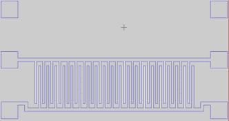
109 SAW Bandpass Filter Interdigital Capacitors and SAW Resonators Figure 6.5: Layouts of different device structures. 97

110 6.6 Deposition of BST on Chemical Vapor Deposited Diamond BST films were deposited on CVD diamond using the RF magnetron sputtering method. The deposition parameters were varied in order to get the highest possible thickness of the BST layer. It was found that at 200 W RF power there was a good growth rate (23-25 nm/hour) beyond which the RF power started affecting the target. Therefore depositions were done with the standard deposition conditions described in Table3.2 (page number 51) and the time of deposition was increased up to 12 hours to get the desired BST thickness. Since there were two deposited layers on Si substrate (CVD diamond and sputtered BST), θ- 2θ XRD studies were inconclusive due to their relatively low thickness compared to the Si substrate. As mentioned before, the surface roughness of the BST layer was dependent on the diamond layer. Cross-sectional SEM studies showed that there were no adhesion issues with BST on CVD diamond (Figure 6.6). Figure 6.6: Cross-sectional SEM image of BST on CVD diamond. 98


111 6.7 Fabrication of Interdigital Structures The traditional metal lift-off method did not work for the fabrication of the IDT s as particles of the top electrode layer was getting stuck in between the finger gaps in the 2 micron and 3 micron interdigital structures. Therefore a modified fabrication process was followed in which the metal layer was deposited and patterned first and then the gold metal was etched off instead of being lifted-off. Figure 6.7: Photographs of fabricated IDT s with 2 μm and 3 μm finger widths. 99
 and Gold (Au) (where Ti")


112 Figure 6.8: Fabrication process flow of Interdigital structures. The fabrication process was started by first sputtering Titanium (Ti) and Gold (Au) (where Ti is the adhesion layer) on the deposited BST layer. The thicknesses of Ti and Au were 40Å and 3000Å respectively. The wafer was then patterned using conventional lithography techniques using a positive resist in order to pattern the interdigital structures. Finally the Au and the Ti layers were etched off using the respective wet etchants. The etch times for Au and Ti were 3min30sec and 10 seconds respectively. 100
113 The resulting 2 micron and 3 micron interdigital structures were very well-defined. Photographs of fabricated devices are also provided in Figure 6.7. The process flow of the IDT fabrication is summarized in Figure 6.8. Further study needs to be done by conducting the SEM analysis of the fabricated interdigital structures to conform the absence of top electrode particles in between the electrode fingers. 6.8 Curie Temperature Measurements on Ba 0.8 Sr 0.2 TiO 3 Curie temperature measurements were done in order to determine the temperature range up to which the deposited BST films exhibit ferroelectricity. The measurements were done on Interdigital Capacitor (IDC) structures. 25 IDC structures with geometry variations identical to the SAW bandpass structures were designed specifically for these measurements. The schematic of the IDC structures are shown in Figure 6.9. BST films were deposited on 4-inch high resistivity silicon samples using the RF magnetron sputtering process using standardized deposition conditions except for the deposition time which was increased from the usual 4 hours to 8hrs, 10hrs and 12 hrs respectively. It was observed that with increase in the deposition time, the uniformity of the BST film got affected. For a 4hour deposition the variation in thickness from centers to edge of the sample was around 30nm. For an 8 hour deposition the variation in thickness from centre to edge was around 135nm. The variation in thicknesses from the edges to the centre of the sample is provided in Table 6.3. In general, an area of about one inch in the sample showed uniform thickness with increase in deposition time and the devices of interest were fabricated in this area. A schematic of the appearance of the 4-inch sample after a 12 hour BST deposition is shown in Figure


114 Figure 6.9: Schematic of Interdigital capacitor structure used for Curie temperature measurements. Figure 6.10: Schematic of appearance of the 4-inch sample after deposition of BST for 12 hours with different colors representing different thicknesses. 102

115 Table 6.3: Variation in thickness of BST layer with different deposition times. Cascade Microtech system with Cryogenic temperature control was used for the measurements. The capacitance was calculated with change in temperature to determine the Curie temperature [113]. Two-port S-parameter measurements were performed on the fabricated IDC structures. The calibration was done from 1GHz to 7 GHz using the TRL calibration technique. The temperature was varied from -15ºC to 120ºC (Curie temperature of Barium Titanate). The capacitance was calculated at different temperatures was used to plot the capacitance vs. temperature graph for determining the transition region. The equivalent circuit diagram used for extracting the capacitance values is shown in Figure Figure 6.11: Equivalent circuit diagram used for characterizing IDC performance. 103
116 The temperature vs. capacitance measurements obtained for the interdigital capacitor is shown in Figure The measured IDC had 30 finger pairs with a finger width of 5 μm. The aperture of the IDC was microns and IDT length was 125 microns. The device was fabricated on the area of the wafer where the deposited BST thickness was 400 nm (deposition time-10 hours). The measurements (refer to Figure 6.12) indicated that the Curie temperature of the deposited BST films occurred around the 20 degrees Celsius mark which is well below the theoretical Curie temperature of Ba 0.8 Sr 0.2 TiO 3 (77ºC) [64]. This could be due to the shift in apparent Curie temperature due to thickness effects. Further research work is necessary to determine the various factors that affect the Curie temperature of BST in order to obtain films that are ferroelectric (and hence piezoelectric) for underwater SAW applications Capacitance (pf) Temperature (degrees celsius) Figure 6.12: Temperature versus capacitance measurements obtained from the measured Interdigital capacitor. 104
117 CHAPTER 7: CONCLUSIONS AND FUTURE WORK 7.1 BST Deposition and Structural Characterization RF magnetron sputtering method was employed to deposit Ba 0.5 Sr 0.5 TiO 3 thin films on Pt/Ti/SiO 2 /Si bottom electrode stack and the deposition conditions were optimized to obviate the shorting problems in BST varactors and improve the dielectric strength of the deposited BST films. XRD and AFM were used for structural characterization of the deposited BST films. The change in deposition conditions did not cause any discernible change in the structural properties of the deposited films. BST films were then deposited on Pt/NCD/Si electrode stack and the structural characteristics of the deposited films were then compared with those deposited on Pt/Ti/SiO 2 /Si wafer. NCD was deposited on Si wafer by the MPECVD technique. The BST films deposited on Pt/NCD/Si displayed more defects and much higher surface roughness due to the comparatively high roughness of the diamond layer. The stoichiometry of the deposited BST thin films need to studied by using Rutherford Back Scattering (RBS) technique to further optimize the deposition process by compensating for the stoichiometric mismatch between the BST target used for deposition and the sputtered BST film. 105
118 The deposition process can be modified by reducing the RF power in order to get larger grains and reduce the density of grain boundaries especially for nanoscale devices to reduce the statistical variations in properties of devices fabricated on the BST layer. Substrates like MgO and LaAlO 3 can be used to obtain mono-crystalline, epitaxial and textured BST thin films which will translate into better performance of fabricated devices. Bismuth Zinc Niobate (BZN) is currently being researched as an alternative material for varactor applications at high frequencies [38]. Future research work can be conducted on this material and comparisons can be done between BZN varactors and BST varactors. 7.2 Interdiffusion Cross-sectional SEM analysis was done on Pt/Ti/SiO 2 /Si and Pt/NCD/Si electrode stacks after BST deposition. It was observed that the Pt/Ti/SiO 2 /Si displayed heavy interdiffusion between the Ti and Pt layers. The Pt/NCD/Si stack, in comparison displayed stable interfaces between the different layers. This was further conformed by conducting X-ray mapping of the stack. The XRM results also indicated the existence of stable interfaces. The interface analysis of the bottom electrode stack can be further done by using RBS and Transmission Electron Microscopy. 7.3 BST Varactor Fabrication and Measurements BST MIM structures were fabricated using conventional optical lithography and etching techniques. The devices fabricated had large active areas varying from 2500 μm 2 to μm 2. Hence the devices had high capacitance values and lower quality factor values at higher frequencies. 106
119 The performance of the fabricated varactors was characterized from 100 MHz to 1 GHz and measurements revealed that the BST varactors fabricated on Pt/NCD/Si displayed better quality factors and good symmetry in CV characteristics due to the existence of stable interfaces. The varactors fabricated on Pt/Ti/SiO 2 /Si were demonstrated much better reliability and higher breakdown fields. The high surface roughness and inconsistency of BST films on Pt/NCD/Si contributed to the relatively poor reliability and breakdown fields. Based on the results obtained a relation was derived linking the interface quality to the tunability and breakdown voltage in varactors. It was found that thetunability and breakdown of varactors have a direct relation with the BST film thickness. The lower the BST film thickness, the faster the tunability. However bad interfaces restrict the thickness of BST that can be deposited and thereby affect the tuning speed of the varactor. It was concluded that with a good interface and a stable bottom electrode it is possible to tailor the performance of the varactors to suit various applications. Thus with the realization of a robust NCD based MIM structure, a good all-round varactor performance can be obtained. Further work needs to be done to improve the structural properties of the BST films deposited on MPECVD diamond based electrode stack. BST nano-scale varactors that operate efficiently at frequencies >1 GHz have been fabricated by employing the Focused Ion Beam (FIB) milling technique [114]. A schematic of the fabricated series-gap capacitor structure is shown in Figure
 for pulse shaping and pulse modulation, frequency multipliers and non-linear antennas. Figure 7.1: FIB milled BST series gap capacitor configuration.")
120 Future work in this area will be on investigating the non-linear properties of nano-scale active regions of BST thin films for developing Non-Linear Transmission Lines (NLTL s) for pulse shaping and pulse modulation, frequency multipliers and non-linear antennas. Figure 7.1: FIB milled BST series gap capacitor configuration. 108
Ferroelectric materials contain one or more polar axes along which a spontaneous
 Chapter 3 Ferroelectrics 3.1 Definition and properties Ferroelectric materials contain one or more polar axes along which a spontaneous polarization can be developed below the material s Curie temperature.
Thin Film Bi-based Perovskites for High Energy Density Capacitor Applications
 ..SKELETON.. Thin Film Bi-based Perovskites for High Energy Density Capacitor Applications Colin Shear Advisor: Dr. Brady Gibbons 2010 Table of Contents Chapter 1 Introduction... 1 1.1 Motivation and Objective...
Addition 1. Shear Stack Piezoelectric Elements and Shear Effect Basics
 120 Addition 1 Shear Stack Piezoelectric Elements and Shear Effect Basics Introduction The STM scanner built up in this work is a Besocke type scanner (see room temperature STM instrumental chapter). The
Classification of Dielectrics & Applications
 Classification of Dielectrics & Applications DIELECTRICS Non-Centro- Symmetric Piezoelectric Centro- Symmetric Pyroelectric Non- Pyroelectric Ferroelectrics Non-Ferroelectric Piezoelectric Effect When
Introduction to solid state physics
 PHYS 342/555 Introduction to solid state physics Instructor: Dr. Pengcheng Dai Professor of Physics The University of Tennessee (Room 407A, Nielsen, 974-1509) Chapter 13: Dielectrics and ferroelectrics
CHAPTER 6 DIELECTRIC AND CONDUCTIVITY STUDIES OF ZIRCONIUM TIN TITANATE (ZST)
") 123 CHAPTER 6 DIELECTRIC AND CONDUCTIVITY STUDIES OF ZIRCONIUM TIN TITANATE (ZST) 6.1 INTRODUCTION We know that zirconium tin titanate ceramics are mostly used in microwave frequency applications. Previous
123 CHAPTER 6 DIELECTRIC AND CONDUCTIVITY STUDIES OF ZIRCONIUM TIN TITANATE (ZST) 6.1 INTRODUCTION We know that zirconium tin titanate ceramics are mostly used in microwave frequency applications. Previous
ESO 205 Nature and Properties of Materials
 Dielectric Materials Topics to discuss Principles of dielectrics Dielectrics Loss and Breakdown Polarizations Frequency dependence Ferro-, Piezo- and Pyro- electrics ESO 205 Nature and Properties of Materials
5. Building Blocks I: Ferroelectric inorganic micro- and nano(shell) tubes
 tubes") 5. Building Blocks I: Ferroelectric inorganic micro- and nano(shell) tubes 5.1 New candidates for nanoelectronics: ferroelectric nanotubes In this chapter, one of the core elements for a complex building
5. Building Blocks I: Ferroelectric inorganic micro- and nano(shell) tubes 5.1 New candidates for nanoelectronics: ferroelectric nanotubes In this chapter, one of the core elements for a complex building
User s Manual. STUDY OF DIELECTRIC CONSTANT Model: DEC-01
 User s Manual STUDY OF DIELECTRIC CONSTANT Model: DEC-01 Manufactured by.. Scientific Equipment & Services 358/1, New Adarsh Nagar, Roorkee - 247 667, UA, INDIA Ph.: +91-1332-272852, 277118 Fax: +91-1332-274831
MME 467: Ceramics for Advanced Applications
 MME 467: Ceramics for Advanced Applications Lecture 26 Dielectric Properties of Ceramic Materials 2 1. Barsoum, Fundamental Ceramics, McGraw-Hill, 2000, pp.513 543 2. Richerson, Modern Ceramic Engineering,
CHAPTER-4 Dielectric Study
 CHAPTER-4 Dielectric Study Dielectric Study 4.1 Introduction The characterization of dielectric ceramics has received considerable scientific interest because of their enormous applications in electronic
Chapter 3 Chapter 4 Chapter 5
 Preamble In recent years bismuth-based, layer-structured perovskites such as SrBi 2 Nb 2 O 9 (SBN) and SrBi 2 Ta 2 O 9 (SBT) have been investigated extensively, because of their potential use in ferroelectric
Chap. 7. Dielectric Materials and Insulation
 Chap. 7. Dielectric Materials and Insulation - The parallel plate capacitor with free space as an insulator: - The electric dipole moment for a pair of opposite changes +Q and -Q separated by a finite
Ferroelectric Materials
 Ferroelectric Materials The permanent electric dipole moment possessed by all pyroelectric [polar] materials may, in certain cases, be reoriented by the application of an electric field. Such crystals
Dielectric Materials: Properties and Applications
 Dielectric Materials: Properties and Applications Content 1. Dielectrics : Properties 2. Fundamental definitions and Properties of electric dipole 3. Various polarization mechanisms involved in dielectric
SURFACE ACOUSTIC WAVE FERROELECTRIC PHONONIC CRYSTAL TUNABLE BY ELECTRIC FIELD
 NANOSYSTEMS: PHYSICS, CHEMISTRY, MATHEMATICS, 2013, 4 (5), P. 630 634 SURFACE ACOUSTIC WAVE FERROELECTRIC PHONONIC CRYSTAL TUNABLE BY ELECTRIC FIELD V. P. Pashchenko 1,2 1 Saint Petersburg State Polytechnical
Piezo materials. Actuators Sensors Generators Transducers. Piezoelectric materials may be used to produce e.g.: Piezo materials Ver1404
 Noliac Group develops and manufactures piezoelectric materials based on modified lead zirconate titanate (PZT) of high quality and tailored for custom specifications. Piezoelectric materials may be used
Dielectric Properties of Solids
 Dielectric Properties of Solids Electric polarization In an insulator the electrons are so tightly bound that at ordinary temperatures they cannot be dislodged either by thermal vibrations or with ordinary
PIEZOELECTRIC TECHNOLOGY PRIMER
 PIEZOELECTRIC TECHNOLOGY PRIMER James R. Phillips Sr. Member of Technical Staff CTS Wireless Components 4800 Alameda Blvd. N.E. Albuquerque, New Mexico 87113 Piezoelectricity The piezoelectric effect is
COURSE OUTLINE. Introduction Signals and Noise Filtering Sensors: Piezoelectric Force Sensors. Sensors, Signals and Noise 1
 Sensors, Signals and Noise 1 COURSE OUTLINE Introduction Signals and Noise Filtering Sensors: Piezoelectric Force Sensors Piezoelectric Force Sensors 2 Piezoelectric Effect and Materials Piezoelectric
DEPOSITION OF THIN TiO 2 FILMS BY DC MAGNETRON SPUTTERING METHOD
 Chapter 4 DEPOSITION OF THIN TiO 2 FILMS BY DC MAGNETRON SPUTTERING METHOD 4.1 INTRODUCTION Sputter deposition process is another old technique being used in modern semiconductor industries. Sputtering
DIELECTRIC AND TUNABLE BEHAVIOR OF LEAD STRONTIUM TITANATE CERAMICS AND COMPOSITES
 The Pennsylvania State University The Graduate School Intercollege Graduate Program in Materials DIELECTRIC AND TUNABLE BEHAVIOR OF LEAD STRONTIUM TITANATE CERAMICS AND COMPOSITES A Thesis in Materials
Transformation dependence of lead zirconate titanate (PZT) as shown by PiezoAFM surface mapping of Sol-gel produced PZT on various substrates.
 as shown by PiezoAFM surface mapping of Sol-gel produced PZT on various substrates.") Transformation dependence of lead zirconate titanate (PZT) as shown by PiezoAFM surface mapping of Sol-gel produced PZT on various substrates. Abstract S. Dunn and R. W. Whatmore Building 70, Nanotechnology,
Transformation dependence of lead zirconate titanate (PZT) as shown by PiezoAFM surface mapping of Sol-gel produced PZT on various substrates. Abstract S. Dunn and R. W. Whatmore Building 70, Nanotechnology,
Relaxor characteristics of ferroelectric BaZr 0.2 Ti 0.8 O 3 ceramics
 Materials Science-Poland, Vol. 27, No. 3, 2009 Relaxor characteristics of ferroelectric BaZr 0.2 Ti 0.8 O 3 ceramics C. FU 1, 2*, F. PAN 1, W. CAI 1, 2, X. DENG 2, X. LIU 2 1 School of Materials Science
Electrical Properties
 Electrical Properties Electrical Conduction R Ohm s law V = IR I l Area, A V where I is current (Ampere), V is voltage (Volts) and R is the resistance (Ohms or ) of the conductor Resistivity Resistivity,
Room-temperature tunable microwave properties of strained SrTiO 3 films
 JOURNAL OF APPLIED PHYSICS VOLUME 96, NUMBER 11 1 DECEMBER 2004 Room-temperature tunable microwave properties of ed SrTiO 3 films Wontae Chang, a) Steven W. Kirchoefer, Jeffrey M. Pond, Jeffrey A. Bellotti,
Dielectric, Piezoelectric and Nonlinear Optical Properties of Lead Titanate based Ferroelectric Thin films
 Dielectric, Piezoelectric and Nonlinear Optical Properties of Lead Titanate based Ferroelectric Thin films Ferroelectric oxides with perovskite structure has gained lot of interest from research as well
Polarization. D =e i E=k i e o E =e o E+ P
 Dielectrics Polarization a perfect insulator or a dielectric is the material with no free charge carriers. if an electric field, E, is applied to the insulator no charge flow. However in the presence of
Roger Johnson Structure and Dynamics: Displacive phase transition Lecture 9
 9.1. Summary In this Lecture we will consider structural phase transitions characterised by atomic displacements, which result in a low temperature structure that is distorted compared to a higher temperature,
Chapter 6 ELECTRICAL CONDUCTIVITY ANALYSIS
 Chapter 6 ELECTRICAL CONDUCTIVITY ANALYSIS CHAPTER-6 6.1 Introduction The suitability and potentiality of a material for device applications can be determined from the frequency and temperature response
Objective: Competitive Low-Cost Thin-Film Varactor Technology. Integrated Monolithic Capacitors using Sputtered/MOCVD material on low-cost substrates
 Overview of Program Objective: Competitive Low-Cost Thin-Film Varactor Technology coplanar waveguide (CPW) capacitor ground signal ground Si substrate etched troughs Focus of Our Program! Reproducibility!
The Science & Engineering of Materials Semiconductors. 주요반도체재료에서전자와홀의 mobility 대표적인값은? 어떤 carrier 가빠른지?
 18.6 Semiconductors 주요반도체재료에서전자와홀의 mobility 대표적인값은? 어떤 carrier 가빠른지? 18.6 Semiconductors [Fig. 18-16] - + When a voltage is applied to a semiconductor, the electrons move through the conduction band, while
Phase Transitions in Relaxor Ferroelectrics
 Phase Transitions in Relaxor Ferroelectrics Matthew Delgado December 13, 2005 Abstract This paper covers the properties of relaxor ferroelectrics and considers the transition from the paraelectric state
Transduction Based on Changes in the Energy Stored in an Electrical Field
 Lecture 7-1 Transduction Based on Changes in the Energy Stored in an Electrical Field - Electrostriction The electrostrictive effect is a quadratic dependence of strain or stress on the polarization P
Ferroelectrics in agile microwave components
 rmenian Journal of Physics, 2009, vol. 2, issue 1, p. 64-70 Ferroelectrics in agile microwave components Spartak Gevorgian Department of Microtechnology and Nanoscience, Chalmers University of Technology,
Ferroelectricity. Phase transition. Material properties. 4/12/2011 Physics 403 Spring
 Ferroelectricity. Phase transition. Material properties 4/12/211 Physics 43 Spring 211 1 Ferroelectricity. outline Ferroelectricity. Definition Discovery Main properties Phenomenological theory Some materials
Self-study problems and questions Processing and Device Technology, FFF110/FYSD13
 Self-study problems and questions Processing and Device Technology, FFF110/FYSD13 Version 2016_01 In addition to the problems discussed at the seminars and at the lectures, you can use this set of problems
Creation of DIPOLE (two poles) (distortion of crystal structure by the small displacement of the ion in direction of electric field)
 (distortion of crystal structure by the small displacement of the ion in direction of electric field)") Dielectricity Dielectric materials: Materials which is generally insulators. Under applied electric field, there is a tiny movement of charge inside the material. Electric field Creation of DIPOLE (two
Dielectricity Dielectric materials: Materials which is generally insulators. Under applied electric field, there is a tiny movement of charge inside the material. Electric field Creation of DIPOLE (two
Modeling Polarization and Capacitance Hysteresis of Ferroelectric Capacitors
 University of Texas at Tyler Scholar Works at UT Tyler Electrical Engineering Theses Electrical Engineering Spring 4-30-2012 Modeling Polarization and Capacitance Hysteresis of Ferroelectric Capacitors
High tunable dielectric response of Pb 0.87 Ba 0.1 La 0.02 (Zr 0.6 Sn 0.33 Ti 0.07 ) O 3 thin film
 O 3 thin film") Journal of Applied Physics, 2010, Volume 108, Issue 4, paper number 044107 High tunable dielectric response of Pb 0.87 Ba 0.1 La 0.02 (Zr 0.6 Sn 0.33 Ti 0.07 ) O 3 thin film T. M. Correia and Q. Zhang*
Journal of Applied Physics, 2010, Volume 108, Issue 4, paper number 044107 High tunable dielectric response of Pb 0.87 Ba 0.1 La 0.02 (Zr 0.6 Sn 0.33 Ti 0.07 ) O 3 thin film T. M. Correia and Q. Zhang*
Monte Carlo Simulation of Ferroelectric Domain Structure: Electrostatic and Elastic Strain Energy Contributions
 Monte Carlo Simulation of Ferroelectric Domain Structure: Electrostatic and Elastic Strain Energy Contributions B.G. Potter, Jr., B.A. Tuttle, and V. Tikare Sandia National Laboratories Albuquerque, NM
UNIVERSITY OF CALIFORNIA College of Engineering Department of Electrical Engineering and Computer Sciences. Fall Exam 1
 UNIVERSITY OF CALIFORNIA College of Engineering Department of Electrical Engineering and Computer Sciences EECS 143 Fall 2008 Exam 1 Professor Ali Javey Answer Key Name: SID: 1337 Closed book. One sheet
Supplementary Information
 Supplementary Information Large Electrocaloric Effect in Relaxor Ferroelectric and Antiferroelectric Lanthanum Doped Lead Zirconate Titanate Ceramics Biao Lu, Peilian Li, Zhenghua Tang, Yingbang Yao, Xingsen
Institute for Electron Microscopy and Nanoanalysis Graz Centre for Electron Microscopy
 Institute for Electron Microscopy and Nanoanalysis Graz Centre for Electron Microscopy Micromechanics Ass.Prof. Priv.-Doz. DI Dr. Harald Plank a,b a Institute of Electron Microscopy and Nanoanalysis, Graz
CHAPTER-1 INTRODUCTION
 CHAPTER-1 INTRODUCTION 1.1 OVERVIEW In today s microelectronics computer industry, various types of memories are used for the data storage. Generally, memories are categorized into volatile and non-volatile.
A Novel Tunable Dual-Band Bandstop Filter (DBBSF) Using BST Capacitors and Tuning Diode
 Using BST Capacitors and Tuning Diode") Progress In Electromagnetics Research C, Vol. 67, 59 69, 2016 A Novel Tunable Dual-Band Bandstop Filter (DBBSF) Using BST Capacitors and Tuning Diode Hassan Aldeeb and Thottam S. Kalkur * Abstract A novel
Progress In Electromagnetics Research C, Vol. 67, 59 69, 2016 A Novel Tunable Dual-Band Bandstop Filter (DBBSF) Using BST Capacitors and Tuning Diode Hassan Aldeeb and Thottam S. Kalkur * Abstract A novel
I. INTRODUCTION II. SAMPLE PREPARATION JOURNAL OF APPLIED PHYSICS VOLUME 92, NUMBER 5 1 SEPTEMBER
 JOURNAL OF APPLIED PHYSICS VOLUME 92, NUMBER 5 1 SEPTEMBER 2002 Longitudinal and transverse piezoelectric coefficients of lead zirconate titanateõvinylidene fluoride-trifluoroethylene composites with different
Materials 218/UCSB: Phase transitions and polar materials
 Materials 218/UCSB: Phase transitions and polar materials Ram Seshadri (seshadri@mrl.ucsb.edu) Background: Intrinsic stability of thermodynamic systems (after H. B. Callen, Thermodynamics and an introduction
Ferroelectrics investigation
 Ferroelectrics investigation. Introduction A dielectric is understood as a material where the electric field induces an electric momentum. Let s consider a vacuum capacitor made of two planar metallic
G. Ravichandran Aeronautics & Mechanical Engineering Graduate Aeronautical Laboratories California Institute of Technology
 Multi-Disciplinary University Initiative Army Research Office Engineering Microstructural Complexity in Ferroelectric Devices Mechanical Characterization G. Ravichandran Aeronautics & Mechanical Engineering
Epitaxial piezoelectric heterostructures for ultrasound micro-transducers
 15 th Korea-U.S. Forum on Nanotechnology Epitaxial piezoelectric heterostructures for ultrasound micro-transducers Seung-Hyub Baek Center for Electronic Materials Korea Institute of Science and Technology
Supplementary Methods A. Sample fabrication
 Supplementary Methods A. Sample fabrication Supplementary Figure 1(a) shows the SEM photograph of a typical sample, with three suspended graphene resonators in an array. The cross-section schematic is
Materials and Devices in Electrical Engineering
 Examination WS 02/03 Materials and Devices in Electrical Engineering Monday 17 th of March, 9:00 11:00, International Department, SR. 203 Notice 1. It is allowed to use any kind of aids (books, scripts,
Supplementary Figures:
 Supplementary Figures: Supplementary Figure 1 Cross-sectional morphology and Chemical composition. (a) A low-magnification dark-field TEM image shows the cross-sectional morphology of the BWO thin film
MICROWAVE FREQUENCY THIN BST FILM BASED TUNABLE SHUNT AND SERIES INTERDIGITAL CAPACITOR DEVICE DESIGN
 MICROWAVE FREQUENCY THIN BST FILM BASED TUNABLE SHUNT AND SERIES INTERDIGITAL CAPACITOR DEVICE DESIGN Thesis Submitted to The School of Engineering of the UNIVERSITY OF DAYTON In Partial Fulfillment of
Lecture 05 Structure of Ceramics 2 Ref: Barsoum, Fundamentals of Ceramics, Ch03, McGraw-Hill, 2000.
 MME 467 Ceramics for Advanced Applications Lecture 05 Structure of Ceramics 2 Ref: Barsoum, Fundamentals of Ceramics, Ch03, McGraw-Hill, 2000. Prof. A. K. M. Bazlur Rashid Department of MME, BUET, Dhaka
Ferroelectrics. Spartak Gevorgian. Department of Microtechnology and Nanoscience Chalmers University of Technology Gothenburg, Sweden
 Ferroelectrics Material Properties, Processing, and Microwave Applications Spartak Gevorgian Department of Microtechnology and Nanoscience Chalmers University of Technology Gothenburg, Sweden Norwegian
Micro-Brilouin scattering study of field cooling effects on ferroelectric relaxor PZN-9%PT single crystals
 Micro-Brilouin scattering study of field cooling effects on ferroelectric relaxor PZN-9%PT single crystals Jae-Hyeon Ko 1 *, Do Han Kim 2, Seiji Kojima 2, D. C. Feng 3 1 Department of Physics, Hallym University,
Properties of Materials
 Tao Deng, dengtao@sjtu.edu.cn 1 1896 1920 1987 2006 Properties of Materials Chapter 3 Electrical Properties of Materials Tao Deng 3.1.4.4 The superconducting tunneling effect (Josephson effect) Tao Deng,
Recent Developments in Magnetoelectrics Vaijayanti Palkar
 Recent Developments in Magnetoelectrics Vaijayanti Palkar Department of Condensed Matter Physics & Materials Science Tata Institute of Fundamental Research Mumbai 400 005, India. Tata Institute of Fundamental
Structural Analysis and Dielectric Properties of Cobalt Incorporated Barium Titanate
 AMANTULLA MANSURI, ASHUTOSH MISHRA School of Physics, Devi Ahilya University, Khandwa road campus, Indore, 452001, India Corresponding author: a.mansuri14@gmail.com Abstract The polycrystalline samples
Principles of Active Vibration Control: Piezoelectric materials
 Principles of Active Vibration Control: Piezoelectric materials Introduction: Piezoelectric materials are materials that produce a voltage when stress is applied. Since, this effect also applies in the
Phase Transitions in Strontium Titanate
 Phase Transitions in Strontium Titanate Xinyue Fang Department of Physics, University of Illinois at Urbana-Champaign Abstract Strontium Titanate SrTiO 3 (STO) is known to undergo an antiferrodistortive
Pulsed laser deposition of PZT and PLZT
 Chapter 3 Pulsed laser deposition of PZT and PLZT A lower growth temperature of PZT films is favored for integration of these films for MEMS application. This chapter gives a detailed account of the work
Dielectric, Ferroelectric, and Optical Properties
 NE3rd.book Seite 33 Dienstag, 4. Februar 0 7:4 9 Dielectric, Ferroelectric, and Optical Properties Susanne Hoffmann-Eifert, Peter Grünberg Institute & JARA-FIT, Forschungszentrum Jülich, Germany Dieter
MODELING OF CV CHARACTERISTICS OF HIGH-k MIM CAPACITORS
 Chapter 6 MODELING OF CV CHARACTERISTICS OF HIGH-k MIM CAPACITORS 6.1 Introduction and Motivation Capacitance-Voltage characteristics and voltage linearity of MIM capacitor are important performance parameters
ME 515 Mechatronics. Overview of Computer based Control System
 ME 515 Mechatronics Introduction to Sensors I Asanga Ratnaweera Department of Faculty of Engineering University of Peradeniya Tel: 081239 (3627) Email: asangar@pdn.ac.lk Overview of Computer based Control
Advanced Vitreous State The Physical Properties of Glass
 Advanced Vitreous State The Physical Properties of Glass Dielectric Properties of Glass Lecture 1: Dielectric in Static Field Himanshu Jain Department of Materials Science & Engineering Lehigh University,
Synthesis and Ferroelectric Properties of KNO 3 films
 Synthesis and Ferroelectric Properties of KNO 3 films Shahid Ramay and Muhammad Sabieh Anwar LUMS School of Science and Engineering Friday, August, 20, 2010 Potassium nitrate (KNO 3 ) shows ferroelectric
Solid State Science and Technology, Vol. 13, No 1 & 2 (2005) ISSN
 ISSN") FABRICATION OF Bi-Ti-O THIN FILM PRESSURE SENSOR PREPARED BY ELECTRON BEAM EVAPORATION METHOD Chong Cheong Wei, Muhammad Yahaya and Muhamad Mat Salleh Institue of Microengineering and Nanoelectronics,
FABRICATION OF Bi-Ti-O THIN FILM PRESSURE SENSOR PREPARED BY ELECTRON BEAM EVAPORATION METHOD Chong Cheong Wei, Muhammad Yahaya and Muhamad Mat Salleh Institue of Microengineering and Nanoelectronics,
Piezo Theory: Chapter 1 - Physics & Design
 Piezoelectric effect inverse piezoelectric effect The result of external forces to a piezoelectric material is positive and negative electrical charges at the surface of the material. If electrodes are
Ferroelectricity. Phase transition. Material properties
 Ferroelectricity. Phase transition. Material properties BaTiO 3 DKDP KDP PZN-PT(9%) PMN-PT(30%) PMN-PT(40%) 4/1/2016 Physics 403 Spring 2016 1 Ferroelectricity. outline Ferroelectricity. Definition Discovery
Depolarization of a piezoelectric film under an alternating current field
 JOURNAL OF APPLIED PHYSICS 101, 054108 2007 Depolarization of a piezoelectric film under an alternating current field K. W. Kwok, a M. K. Cheung, H. L. W. Chan, and C. L. Choy Department of Applied Physics
The Pennsylvania State University. The Graduate School. College of Engineering ON THE IMPACT OF ELECTRODE GEOMETRY ON THE PIEZOELECTRIC
 The Pennsylvania State University The Graduate School College of Engineering ON THE IMPACT OF ELECTRODE GEOMETRY ON THE PIEZOELECTRIC PROPERTIES OF PZT 5A FIBERS A Thesis in Mechanical Engineering by Travis
Materials and Devices in Electrical Engineering
 Examination WS 01/02 Materials and Devices in Electrical Engineering Monday 11 th of March, 9:00 to 11:00, SR 203, International Department building It is allowed to use any kind of media (books, scripts,
1. Chapter 1: Introduction
 1. Chapter 1: Introduction Non-volatile memories with ferroelectric capacitor materials are also known as ferroelectric random access memories (FRAMs). Present research focuses on integration of ferroelectric
Investigation of Loss Mechanisms in Thin Film Barium Strontium Titanate Capacitors
 UNIVERSITY OF CALIFORNIA Santa Barbara Investigation of Loss Mechanisms in Thin Film Barium Strontium Titanate Capacitors A Dissertation submitted in partial satisfaction of the requirements for the degree
The electric field induced strain behavior of single. PZT piezoelectric ceramic fiber
 The electric field induced strain behavior of single PZT piezoelectric ceramic fiber Xiong Yang a, Jing Zhou a,*, Sen Zhang a, Jie Shen b, Jing Tian a, Wen Chen a, Qi Zhang ac a State Key Laboratory of
Paper V. Acoustic Radiation Losses in Busbars. J. Meltaus, S. S. Hong, and V. P. Plessky J. Meltaus, S. S. Hong, V. P. Plessky.
 Paper V Acoustic Radiation Losses in Busbars J. Meltaus, S. S. Hong, and V. P. Plessky 2006 J. Meltaus, S. S. Hong, V. P. Plessky. V Report TKK-F-A848 Submitted to IEEE Transactions on Ultrasonics, Ferroelectrics,
Solid State Physics (condensed matter): FERROELECTRICS
: FERROELECTRICS") Solid State Physics (condensed matter): FERROELECTRICS Prof. Igor Ostrovskii The University of Mississippi Department of Physics and Astronomy Oxford, UM: May, 2012 1 People: Solid State Physics Condensed
Solid State Physics (condensed matter): FERROELECTRICS Prof. Igor Ostrovskii The University of Mississippi Department of Physics and Astronomy Oxford, UM: May, 2012 1 People: Solid State Physics Condensed
ELECTRONICS DEVICES AND MATERIALS
 2-2-2 ELECTRONICS DEVICES AND MATERIALS Atsunori KAMEGAWA SYLLABUS! Introduction to materials structure and dielectric physics (04/27)! Ferroelectricity involved in structural phase transitions (05/25)
Condensed Matter A Week 2: Crystal structure (II)
") QUEEN MARY, UNIVERSITY OF LONDON SCHOOL OF PHYSICS AND ASTRONOMY Condensed Matter A Week : Crystal structure (II) References for crystal structure: Dove chapters 3; Sidebottom chapter. Last week we learnt
QUEEN MARY, UNIVERSITY OF LONDON SCHOOL OF PHYSICS AND ASTRONOMY Condensed Matter A Week : Crystal structure (II) References for crystal structure: Dove chapters 3; Sidebottom chapter. Last week we learnt
Chapter 2. Dielectric Theories
 Chapter Dielectric Theories . Dielectric Theories 1.1. Introduction Measurements of dielectric properties of materials is very important because it provide vital information regarding the material characteristics,
RECONFIGURABLE PASSIVE RF/MICROWAVE COMPONENTS. Dissertation. Submitted to. The School of Engineering of the UNIVERSITY OF DAYTON
 RECONFIGURABLE PASSIVE RF/MICROWAVE COMPONENTS Dissertation Submitted to The School of Engineering of the UNIVERSITY OF DAYTON In Partial Fulfillment of the Requirements for The Degree of Doctor of Philosophy
Micromechanical modeling and simulation of piezoceramic materials
 Micromechanical modeling and simulation of piezoceramic materials B. Delibas 1, A. Arockia Rajan 1 & W. Seemann 2 1 Workgroup for Machine Dynamics, Technical University of Kaiserslautern, Germany 2 Institut
Effect of grain size on the electrical properties of Ba,Ca Zr,Ti O 3 relaxor ferroelectric ceramics
 JOURNAL OF APPLIED PHYSICS 97, 034109 (2005) Effect of grain size on the electrical properties of Ba,Ca Zr,Ti O 3 relaxor ferroelectric ceramics Xin-Gui Tang a) Faculty of Applied Physics, Guangdong University
Table of Contents. Chapter 1. Dielectricity, Piezoelectricity, Pyroelectricity and Ferroelectricity... 1
 Preface... General Introduction... xiii xvii Chapter 1. Dielectricity, Piezoelectricity, Pyroelectricity and Ferroelectricity.... 1 1.1. Crystal structure... 1 1.1.1. Crystal = lattice + pattern... 1 1.1.2.
Structural and electrical characterization of epitaxial, large area ferroelectric films of Ba 2 Bi 4 Ti 5 O 18 grown by pulsed excimer laser ablation
 JOURNAL OF APPLIED PHYSICS VOLUME 87, NUMBER 6 15 MARCH 2000 Structural and electrical characterization of epitaxial, large area ferroelectric films of Ba 2 Bi 4 Ti 5 O 18 grown by pulsed excimer laser
The Power of Feedback: From Dielectric to Ferroelectric Systems
 140 International Journal of Plasma Environmental Science & Technology, Vol.10, No.2, DECEMBER 2016 The Power of Feedback: From Dielectric to Ferroelectric Systems H. Kliem and A. Leschhorn Institute of
Multilayer Ceramic Capacitors: Mitigating Rising Failure Rates
 Multilayer Ceramic Capacitors: Mitigating Rising Failure Rates Dock Brown DfR Solutions Seattle, WA Abstract The multilayer ceramic capacitor (MLCC) has become a widely used electronics component both
Effects of plasma treatment on the precipitation of fluorine-doped silicon oxide
 ARTICLE IN PRESS Journal of Physics and Chemistry of Solids 69 (2008) 555 560 www.elsevier.com/locate/jpcs Effects of plasma treatment on the precipitation of fluorine-doped silicon oxide Jun Wu a,, Ying-Lang
Domain switching and electromechanical properties of pulse poled Pb Zn 1Õ3 Nb 2Õ3 O 3 PbTiO 3 crystals
 JOURNAL OF APPLIED PHYSICS VOLUME 89, NUMBER 1 1 JANUARY 2001 Domain switching and electromechanical properties of pulse poled Pb Zn 1Õ3 Nb 2Õ3 O 3 PbTiO 3 crystals Hanxing Yu, Venkat Gopalan, Jürgen Sindel,
Processing and characterization of ferroelectric thin films obtained by pulsed laser deposition
 ELECTROCERAMICS IX, Cherbourg, 2004. Symp. D: Pyro, Piezo, Ferroelectrics: B1-P-578 Processing and characterization of ferroelectric thin films obtained by pulsed laser deposition F. Craciun a,*, M. Dinescu
Physical and Dielectric Properties of Silver Lithium Niobate Mixed Ceramic System
 American Journal of Materials Science and Engineering, 213, Vol. 1, No. 3, 54-59 Available online at http://pubs.sciepub.com/ajmse/1/3/5 Science and Education Publishing DOI:1.12691/ajmse-1-3-5 Physical
Electric displacement as the fundamental variable in electronic-structure calculations
 Electric displacement as the fundamental variable in electronic-structure calculations CECAM - Centre Européen de Calcul Atomique et Moléculaire EPF Lausanne, Switzerland Conference UC Davis, 6/23/2009
CVD: General considerations.
 CVD: General considerations. PVD: Move material from bulk to thin film form. Limited primarily to metals or simple materials. Limited by thermal stability/vapor pressure considerations. Typically requires
Bridging to the Continuum Scale for Ferroelectric Applications
 Bridging to the Continuum Scale for Ferroelectric Applications Shanfu Zheng and Alberto Cuitiño Mechanical and Aerospace Engineering, Rutgers University Alejandro Strachan Materials Engineering, Purdue
SENSORS and TRANSDUCERS
 SENSORS and TRANSDUCERS Tadeusz Stepinski, Signaler och system The Mechanical Energy Domain Physics Surface acoustic waves Silicon microresonators Variable resistance sensors Piezoelectric sensors Capacitive
Electrical material properties
 Electrical material properties U = I R Ohm s law R = ρ (l/a) ρ resistivity l length σ = 1/ρ σ conductivity A area σ = n q μ n conc. of charge carriers q their charge μ their mobility μ depends on T, defects,
ABSTRACT. AYGÜN, SEYMEN MURAT. Processing Science of Barium Titanate. (Under the direction of Jon-Paul Maria.)
") ABSTRACT AYGÜN, SEYMEN MURAT. Processing Science of Barium Titanate. (Under the direction of Jon-Paul Maria.) Barium titanate and barium strontium titanate thin films were deposited on base metal foils
ABSTRACT AYGÜN, SEYMEN MURAT. Processing Science of Barium Titanate. (Under the direction of Jon-Paul Maria.) Barium titanate and barium strontium titanate thin films were deposited on base metal foils