Invited Paper LA C 5' t k( L ( ( ' SEMICONDUCTOR LASERS. Kerry J. Vahala, John A. Lebens, Charles S. Tsai, Thomas F. Kuech t
|
|
|
- Frederick Chapman
- 5 years ago
- Views:
Transcription
1 A. -. j ) yq/7 Invited Paper LA C 5' t k( L ( ( ' I 7)( QUANTUM WIRE AND QUANTUM DOT SEMICONDUCTOR LASERS L I 1 1f Kerry J. Vahala, John A. Lebens, Charles S. Tsai, Thomas F. Kuech t Peter C. Sercel, Michael E. Hoenk, and Hal Zarem Department of Applied Physics Mail Stop California Institute of Technology Pasadena, California ABSTRACT There is currently great interest in fabrication of structures that are two and three dimensional analogs of the conventional quantum well. We review here the physics behind the use of arrays of such lower dimensional structures in semiconductor laser active layers. Methods which are currently under investigation for producing such structures will be discussed. Quantum wires and quantum dots are two and three dimensional analogs of the conventional quantum well (see Figure 1). A quantum dot, for example, would confine an electron in three dimensions to a size comparable to the de Broglie wavelength of the electron in the crystal. To be useful in a device, arrays of quantum wires and quantum dots must be considered as illustrated in Fig. 1. In such arrays quantum dots and wires composed of a low bandgap material would be imbedded in a higher bandgap host (e.g., GaAs dots in an AlGaAs host). A potentially important application of these structures is to laser diodes.' In such devices, the conventional bulk active layer is replaced with an array of quantum dots or quantum wires. As discussed below, these devices would have many advantages over conventional devices. The most important property of quantum wires and quantum dots as concerns their application to laser diode active layers is their density of states functions. Idealized versions of these functions are presented in Fig. 2 for bulk, conventional quantum well, quantum wire, and quantum dot active layers. In reducing dimension it is apparent that these functions take on more singular behavior. For the quantum dot, the behavior is analogous to the density of states of an atomic system. This narrowing of the density of states function carries over directly into the optical gain spectrum, which, for k-conserving transitions, is proportional to the effective density of states of the electronic system and the Fermi t IBM Thomas J. Watson Research Ctr., Yorktown Heights, N.Y. 120 / SPIE Vol Nonlinear Opt/ca/Materials and Devices for Photon/c Switching (1990)
2 L4:.. 'uantum Wire, Quantum Dot id-ow 2D-QW 3D-OW (a) Potential Barrier (b) (C) Fig. 1. Schematic drawing of quantum wells, wires and dots showing the successive dimensions of confinement. The lower part of the figure shows arrays of these structures suitable for incorporation into the active layer of a semiconductor laser. The structures are formed from low bandgap material imbedded in a higher bandgap host. Density of States Functions BULK 0-WELL D3(E) D2(E) rni Egap E 0-BOX D1(E) Egap D0(E) -/ - E E gap E Fig. 2. Density of states functions for zero-, one-, two-, and three-dimensional systems. The dashed curve indicates approximately the optical gain which results when the medium is inverted. SPIE Vol Nonlinear Optical Materials and Devices for Photonic Switching (1990) / 121

3 occupancy factor giving the strength of the inversion. The dashed curves appearing in Fig. 2 show typical gain spectra for each case. Gain spectrum narrowing is maximum for the quantum dot. In fact, here the gain spectrum width is zero according to this highly sim plified model.(in a more realistic model phonon scattering broadens the transition leaving a Lorentzian lineshape as has been illustrated in the figure.) A laser based on a narrower gain spectrum has many First, it is clear that lower threshold currents are possible since fewer carriers are wasted in regions of the spectral space that are not contributing to lasing action. It is important to note that there is also a significant reduction in the transparency excitation level of the gain medium simply from the reduction of the active layer volume. The resulting reduction in threshold has been exploited in ultra low threshold conventional quantum well semiconductor lasers and can also be exploited in quantum wire and quantum dot semiconductor lasers. Dynamic and spectral properties are also improved in these devices. Consider, for example, the direct modulation speed of a diode laser as determined by the relaxation oscillation corner frequency. The square of this corner frequency is easily shown to vary linearly with the differential gain (i.e., the derivative of gain with respect to carrier density). Differential gain will, roughly speaking, vary inversely with spectral width. Hence, reduced dimension results in higher modulation speeds.1 Using similar arguments it is possible to show that chirp reduction, phase noise reduction, and intensity noise reduction also can result from the reduction of the active layer electronic system dimension.1 The application of quantum well and quantum wire active layers to phase noise reduction and modulation speed enhancement in laser diodes was first discussed in Reference 1. All of the theoretical predictions concerning conventional quantum well active layers have since that time been verified. The fabrication of quantum wires and quantum dots poses many challenging problems. At the present time there are two general approaches being taken. Historically first are a variety of techniques in which a quantum well which has been grown on a substrate is modified for lateral confinement on a nanometer scale. In all of these techniques a nanometer scale pattern is first generated on the sample using lithographic methods such as electron or ion beam lithography. The techniques then diverge in terms of how this pattern is transferred to the quantum well resulting in a quantum wire or a quantum dot. One simple example of this could be referred to as the "cookie cutter" approach. In it the lateral confinement is produced by actually etching away unmasked regions of the quantum well sample.2'3 Although extremely small structures are possible with this approach, the resulting structures suffer from free surface induced nonradiative recombination. Recent efforts in this direction are addressing the issue of surface passivation either by chemical treatment or by actual regrowth on the etched structures. A more sophisticated pattern transfer technique that does not leave behind free surfaces is based on disordering of the quantum well either by ion implantation4 or by diffusion.5 These techniques have produced convincng results and are illustrated by the example in Fig. 3. Here again a mask is patterned onto the surface of a semiconductor, containing in this case a shallow quantum well. The mask is patterned using electron beam lithography and subsequently arrays of silicon lines are deposited in a liftoff process. The silicon then serves as a mask in a shallow zinc diffusion into the quantum well. The diffusion of zinc is known to abruptly disorder a 122 / SPIE Vol Nonlinear Optical Materials and Devices for Photon/c Switching (1990)

4 A12Ga8As Quantum Well Al3 Ga7 As Fig. 3. A schematic drawing of diffusion induced disordering of a shallow quantum well to produce quantum wires. A narrow stripe of silicon is produced by electron beam lithography and subsequent liftoff on the surface of a sample containing a shallow quantum well. The silicon stripe serves as a mask for a zinc diffusion which selectively disorders the quantum well. 20Mm Fig. 4. Secondary electron and cathodoluminescence images of several arrays of wires and an isolated wire. The left half shows the silicon mask as a conventional SEM micrograph. The width of the silicon stripes in the arrays varies from 3700A (upper left array) to 1600A (lower right array). The right half shows the spectrally resolved cathodoluminescence image of the same region at a wavelength of 780 nm. The sample temperature is 77K. SPIE Vol Nonlinear Optical Materials and Devices for Photon/c Switching (1990) / 123
 micrograph of this same region of the sample.")
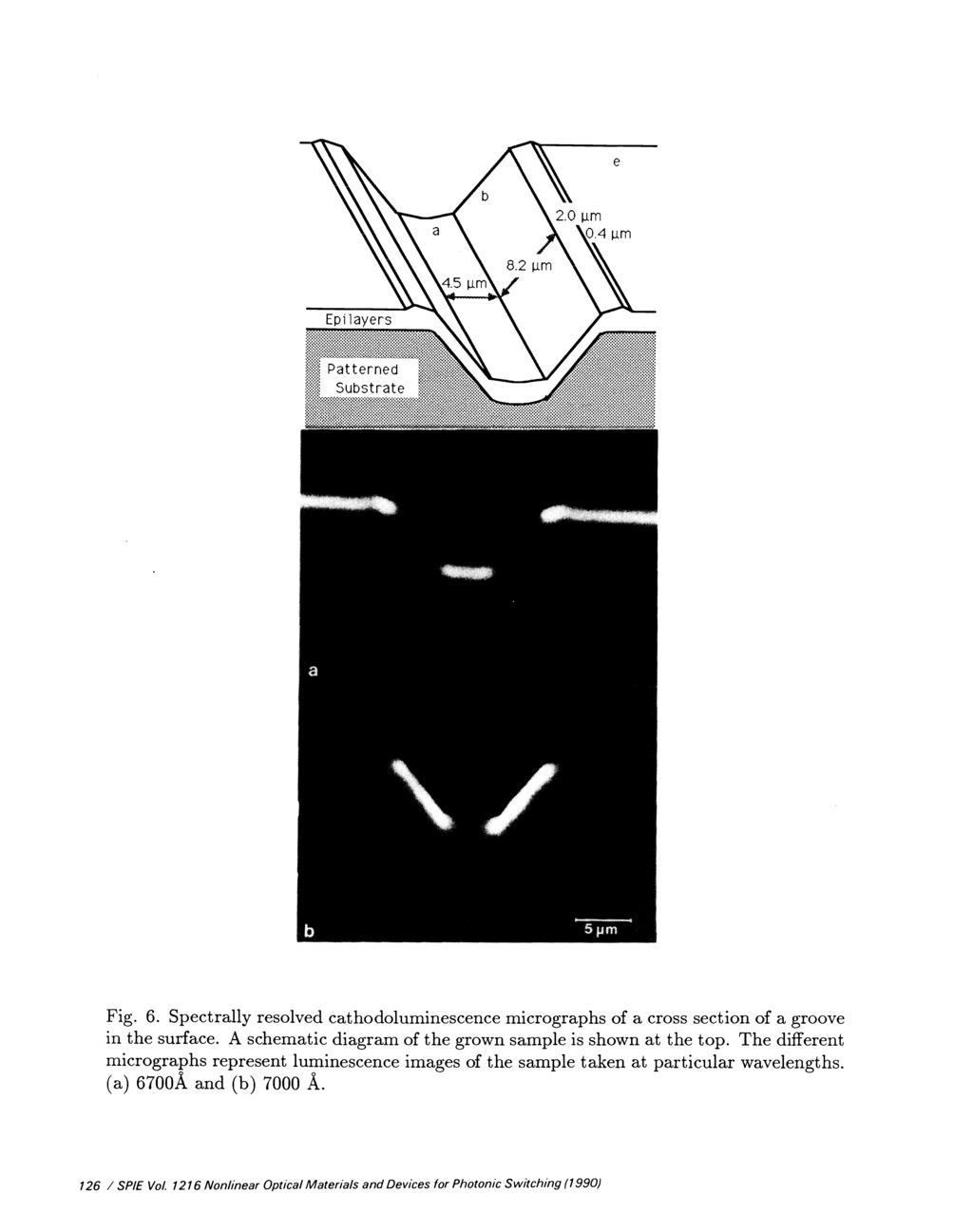
5 quantum well. By timing the diffusion correctly, wire-like regions of low bandgap quantum well material are left behind. Fig. 4 shows a scanning electron micrograph of several silicon arrays with elements of various widths. Also shown in the figure is a cathodoluminescence (CL) micrograph of this same region of the sample. Cathodoluminescence is an alternative means of imaging with a scanning electron microscope. Rather than collecting secondary electrons, CL uses light that is emitted by the recombining electron-hole pairs that have been excited by the electron beam.6 The collected CL emission in this micrograph is spectrally resolved using a grating monochrometer before detection. The wavelength selected is slightly blue shifted from the original quantum well emission peak. The CL image indicates that the quantum well has been successfully disordered in the unmasked regions of the sample. The inability to actually resolve the lines is a consequence of CL's limited spatial resolution which is determined by carrier diffusion. Before discussing the second category of fabrication approaches, it is interesting to consider again the application of these structures to semiconductor laser active layers. In addition to the considerations mentioned earlier, we will now include an additional nonideality that plays a central role in determining the ultimate performance of a quantum wire or quantum dot semiconductor laser. This is fabricational inhomogeneity. Consider, for example, arrays of quantum dots. The confinement energy depends strongly in these structures on the size of the dot. This, in turn, implies that the gain spectrum for an array of quantum dots experiences fabricational induced inhomogeneous broadening. Such broadening tends to counteract the beneficial effects of quantum confinement. The interesting question is therefore: what fabricational tolerance is required if a quantum dot active layer is to outperform a conventional active layer? This question is addressed in Fig. 5 where maximum attainable gain (in both inverse spatial and temporal units) has been plotted for various densities of GaAs quantum dots versus a fabricational RMS variance in dot diameter.7 There are actually two sizes of dots considered in the plot. Large dots having a radius of 100A and small dots having a radius of 50A. Consider the case of small quantum dots with a packing density i = 1.25 x 1017cm3. To attain a maximum optical gain of 120 cm1 (a number typical of bulk GaAs material under high excitation) all dots must be filled with two electrons and two holes (i.e., the equivalent carrier density will be 2.50 x 1017cm3) and a fabrication tolerance of 20A must be maintained. This is well over an order of magnitude better than the bulk material which would only attain these values at carrier densities on the order of 5 x 1018cm3. There are two important points to be made here. First, the above estimate is good news for approaches based on nanolithographic patterning, because although a 20A tolerance on an array of 200A diameter dots exceeds the current state-of-the-art in beam patterning and pattern transfer, it is well within an order of magnitude of what is currently attainable. Second, in considering the figure, it is clear that what is truly needed is a fabrication technology capable of monolayer tolerences, i.e., the equivalent of MBE or MOCVD in the lateral directions. 124 / SPIE Vol Nonlinear Optical Materials and Devices for Photon/c Switching (1990)
6 y- '0 I ci U) 4rrt (_) Q_ % z i:u là 2A 5A ba 20A 50A boa FABRICATION TOLERANCE Fig. 5. Maximum possible optical gain versus fabrication tolerance(given as the rms roughness of dot diameter) for arrays of quantum dots of various dot densities(ijl,iis). Large quantum dots (density ) will have an average diameter of 200A and small quantum dots (density its) have an average diameter of iooa. The cross hatched region is beyond the geometrical packing limit of the quantum boxes. Although such a technology does not yet exist, the second category of techniques are clearly moving in this direction. These are techniques that seek to extend the fabricational control offered by MBE and MOCVD in the z-direction into the x and y-directions. In this way the quantum wires or dots can be formed in the growth process. Examples of these techniques are vicinal growth to produce vertical superlattices8, quantum well thickness control through growth on patterned substrates9, and very recently compositional control through growth on patterned substrates.1 Fig. 6 illustrates the latter of these. The top of Fig. 6 shows a schematic drawing of a substrate patterned by chemically etching a groove. MBE growth of A1GaAs epilayers on such a substrate proceeds along various directions. Surprisingly, under appropriate growth conditions, it has been demonstrated that the (111) growth directions segregate into a quasi periodic structure having a period between 50 70A.1 On the average the composition is uniform, but the microscopic ordering along SPIE Vol Nonlinear Optical Materials and Devices for Photonic Switching (1990) / 125
7 a ca.

8 Fig. 7. SEM micrograph of selectively grown GaAs dots showing faceted nature of growth. SPIE Vol Nonlinear Optical Materials and Devices for Photon/c Switching (1990) / 127

9 the (111) growth directions produces an abrupt lateral change in the effective bandgap energy. This is apparent in Fig. 6 where CL micrographs of groove crossections are shown at two different wavelengths. A new technique which we are currently pursuing is the use of selective epitaxy to grow quantum dot and quantum wire structures.it is related to the above techniques in that the dot structure is formed during growth. It is also related to beam patterning methods descibed earlier since the positions at which the dots or lines are grown is patterned prior to growth. Selective epitaxy refers to a lateral spatially controlled growth of an epitaxial material within openings of a mask material residing on the substrate during growth. The masking material we use is a dielectric layer of Si 3N 4. Recent optimization of growth conditions and selection of growth precursors have produced the high quality growth of GaAs in openings down to the micron scale11. By using electron beam lithography to generate the openings we have successfully grown structures with diameters less than 700A. Fig. 7 shows an SEM micrograph of.25jm GaAs dots grown by this method. These photos illustrate the facetted nature of the growth.by performing a subsequent growth of A1GaAs these GaAs structures can be completely imbedded in a higher bandgap material. We have recently achieved such growth and have seen luminescence from GaAs dots less than ioooa in diameter. In conclusion, the optical properties of arrays of quantum dots and quantum wires have been discussed with emphasis on their application to semiconductor lasers. In addition, a number of approaches to fabrication of these structures have been discussed. Fabrication approaches currently under investigation divide into two broad categories: fabrication based on beam patterning and in-situ fabrication approaches. Extremely good control of fabrication tolerance is essential if quantum wires and quantum dots are to be be useful in semiconductor lasers. With continued refinements in existing fabrication techniques useful quantum wire and quantum dot semiconductor lasers should be possible. To fully tap the performance advantages of these structures, however, will probably require an entirely new fabrication technology. The authors would like to acknowledge the support of the Office of Naval Research and the Strategic Defense Initiative Organization/Innovative Science and Technology. One of us (PS) would like to acknowledge the support of a graduate National Science Foundation fellowship. [1] Y. Arakawa, K. Vahala, A. Yariv, Appl. Phys. Lett., 45, 950 (1984). [2] K. Kash, A. Scherer, J. M. Worlock, H. G. Craighead, M. C. Tamargo, Appl. Phys. Lett., 49, 1043 (1986). [3] II. Temkin, G. J. Dolan, M. B. Panish, S. N. G. Chu, Appi. Phys. Lett., 50, 413 (1987). [4] J. Cibert, P. M. Petroff, G. J. Dolan, S. J. Pearton, A. C. Gossard, J. H. English, Appi. Phys. Lett., 49, 1275 (1986). [5] H. A. Zarem, P. C. Sercel, M. E. Hoenk, J. A. Lebens, K. J. Vahala, Appi. Phys. Lett., 54, 2692 (1989). [6] M. E. Hoenk, K. J. Vahala, Rev. Sci. Instr., 60, 226 (1989). [7] K. J. Vahala, J. Quant. Electron., QE-24, 523 (1988). 128 / SP/E Vol Nonlinear Opt/ca/Materials and Devices for Photon/c Switching (1990)
10 [8] M. Tsuchiya, J. M. Gaines, R. H. Yan, R. J. Simes, P. 0. Holtz, L. A. Coidren, P. M. Petroff, Phys. Rev. Lett., 62, 466 (1989). [9] E. Kapon, S. Simhony, D. M. Hwang, K. Kash, R. Bhat, E. Colas, CLE0 89, Postdeadline Session PD15, Baltimore [10] M. E. Hoenk, C. W. Nieh, H. Chen, K. J. Vahala, Appl. Phys. Lett., 55, 53 (1989) [11] T. F. Kuech, M. A. Tischler, and R. Potemski, Appl. Phys. Lett., 54, 910 (1989). SPIE Vol Nonlinear Optical Materials and Devices for Photonic Switching (1990) / 129
Quantum Dot Lasers. Jose Mayen ECE 355
 Quantum Dot Lasers Jose Mayen ECE 355 Overview of Presentation Quantum Dots Operation Principles Fabrication of Q-dot lasers Advantages over other lasers Characteristics of Q-dot laser Types of Q-dot lasers
Temperature Dependent Optical Band Gap Measurements of III-V films by Low Temperature Photoluminescence Spectroscopy
 Temperature Dependent Optical Band Gap Measurements of III-V films by Low Temperature Photoluminescence Spectroscopy Linda M. Casson, Francis Ndi and Eric Teboul HORIBA Scientific, 3880 Park Avenue, Edison,
Semiconductor Disk Laser on Microchannel Cooler
 Semiconductor Disk Laser on Microchannel Cooler Eckart Gerster An optically pumped semiconductor disk laser with a double-band Bragg reflector mirror is presented. This mirror not only reflects the laser
Photonic Crystal Nanocavities for Efficient Light Confinement and Emission
 Journal of the Korean Physical Society, Vol. 42, No., February 2003, pp. 768 773 Photonic Crystal Nanocavities for Efficient Light Confinement and Emission Axel Scherer, T. Yoshie, M. Lončar, J. Vučković
Segmented 1.55um Laser with 400% Differential Quantum Efficiency J. Getty, E. Skogen, L. Coldren, University of California, Santa Barbara, CA.
 Segmented 1.55um Laser with 400% Differential Quantum Efficiency J. Getty, E. Skogen, L. Coldren, University of California, Santa Barbara, CA. Abstract: By electrically segmenting, and series-connecting
1 Semiconductor Quantum Dots for Ultrafast Optoelectronics
 j1 1 Semiconductor Quantum Dots for Ultrafast Optoelectronics 1.1 The Role of Dimensionality in Semiconductor Materials The history of semiconductor lasers has been punctuated by dramatic revolutions.
Emission Spectra of the typical DH laser
 Emission Spectra of the typical DH laser Emission spectra of a perfect laser above the threshold, the laser may approach near-perfect monochromatic emission with a spectra width in the order of 1 to 10
Signal regeneration - optical amplifiers
 Signal regeneration - optical amplifiers In any atom or solid, the state of the electrons can change by: 1) Stimulated absorption - in the presence of a light wave, a photon is absorbed, the electron is
Ultrafast single photon emitting quantum photonic structures. based on a nano-obelisk
 Ultrafast single photon emitting quantum photonic structures based on a nano-obelisk Je-Hyung Kim, Young-Ho Ko, Su-Hyun Gong, Suk-Min Ko, Yong-Hoon Cho Department of Physics, Graduate School of Nanoscience
Chapter 5. Semiconductor Laser
 Chapter 5 Semiconductor Laser 5.0 Introduction Laser is an acronym for light amplification by stimulated emission of radiation. Albert Einstein in 1917 showed that the process of stimulated emission must
Quantum Dot Lasers Using High-Q Microdisk Cavities
 phys. stat. sol. (b) 224, No. 3, 797 801 (2001) Quantum Dot Lasers Using High-Q Microdisk Cavities P. Michler 1; *Þ (a), A. Kiraz (a), C. Becher (a), Lidong Zhang (a), E. Hu (a), A. Imamoglu (a), W. V.
Photoluminescence characterization of quantum dot laser epitaxy
 Photoluminescence characterization of quantum dot laser epitaxy Y. Li *, Y. C. Xin, H. Su and L. F. Lester Center for High Technology Materials, University of New Mexico 1313 Goddard SE, Albuquerque, NM
Laser Diodes. Revised: 3/14/14 14: , Henry Zmuda Set 6a Laser Diodes 1
 Laser Diodes Revised: 3/14/14 14:03 2014, Henry Zmuda Set 6a Laser Diodes 1 Semiconductor Lasers The simplest laser of all. 2014, Henry Zmuda Set 6a Laser Diodes 2 Semiconductor Lasers 1. Homojunction
M R S Internet Journal of Nitride Semiconductor Research
 M R S Internet Journal of Nitride Semiconductor Research Volume 2, Article 25 Properties of the Biexciton and the Electron-Hole-Plasma in Highly Excited GaN J.-Chr. Holst, L. Eckey, A. Hoffmann, I. Broser
Spectroscopy of. Semiconductors. Luminescence OXFORD IVAN PELANT. Academy ofsciences of the Czech Republic, Prague JAN VALENTA
 Luminescence Spectroscopy of Semiconductors IVAN PELANT Institute ofphysics, v.v.i. Academy ofsciences of the Czech Republic, Prague JAN VALENTA Department of Chemical Physics and Optics Charles University,
Luminescence basics. Slide # 1
 Luminescence basics Types of luminescence Cathodoluminescence: Luminescence due to recombination of EHPs created by energetic electrons. Example: CL mapping system Photoluminescence: Luminescence due to
Self-Assembled InAs Quantum Dots
 Self-Assembled InAs Quantum Dots Steve Lyon Department of Electrical Engineering What are semiconductors What are semiconductor quantum dots How do we make (grow) InAs dots What are some of the properties
SUPPLEMENTARY INFORMATION
 doi:10.1038/nature12036 We provide in the following additional experimental data and details on our demonstration of an electrically pumped exciton-polariton laser by supplementing optical and electrical
Electron Energy, E E = 0. Free electron. 3s Band 2p Band Overlapping energy bands. 3p 3s 2p 2s. 2s Band. Electrons. 1s ATOM SOLID.
 Electron Energy, E Free electron Vacuum level 3p 3s 2p 2s 2s Band 3s Band 2p Band Overlapping energy bands Electrons E = 0 1s ATOM 1s SOLID In a metal the various energy bands overlap to give a single
Linearly polarized and time-resolved cathodoluminescence study of straininduced laterally ordered (InP) 2 /(GaP) 2 quantum wires
 2 /(GaP) 2 quantum wires") Linearly polarized and time-resolved cathodoluminescence study of straininduced laterally ordered (InP) /(GaP) quantum wires D. H. Rich, a) Y. Tang, and H. T. Lin Department of Materials Science and Engineering,
Linearly polarized and time-resolved cathodoluminescence study of straininduced laterally ordered (InP) /(GaP) quantum wires D. H. Rich, a) Y. Tang, and H. T. Lin Department of Materials Science and Engineering,
ISSN Review. Progress to a Gallium-Arsenide Deep-Center Laser
 Materials 2009, 2, 1599-1635; doi:10.3390/ma2041599 OPEN ACCESS materials ISSN 1996-1944 www.mdpi.com/journal/materials Review Progress to a Gallium-Arsenide Deep-Center Laser Janet L. Pan Yale University,
Introduction to Semiconductor Integrated Optics
 Introduction to Semiconductor Integrated Optics Hans P. Zappe Artech House Boston London Contents acknowledgments reface itroduction Chapter 1 Basic Electromagnetics 1 1.1 General Relationships 1 1.1.1
Self-Assembled InAs Quantum Dots on Patterned InP Substrates
 Self-Assembled InAs Quantum Dots on Patterned InP Substrates J. Lefebvre, P.J. Poole, J. Fraser, G.C. Aers, D. Chithrani, and R.L. Williams Institute for Microstructural Sciences, National Research Council
Defense Technical Information Center Compilation Part Notice
 UNCLASSIFIED Defense Technical Information Center Compilation Part Notice ADP012815 TITLE: Resonant Waveguiding and Lasing in Structures with InAs Submonolayers in an AJGaAs Matrix DISTRIBUTION: Approved
Blue-green Emitting Semiconductor Disk Lasers with Intra-Cavity Frequency Doubling
 Blue-green Emitting Semiconductor Disk Lasers with Intra-Cavity Frequency Doubling Eckart Schiehlen and Michael Riedl Diode-pumped semiconductor disk lasers, also referred to as VECSEL (Vertical External
Broadband Quantum-Dot/Dash Lasers
 Broadband Quantum-Dot/Dash Lasers Boon S. Ooi, Electrical & Computer Eng. Lehigh University Tel: 610-758 2606, email:bsooi@lehigh.edu ACKNOWDLEDGEMENT Students and Postdoc: Hery S. Djie, Yang Wang, Clara
Correlated 2D Electron Aspects of the Quantum Hall Effect
 Correlated 2D Electron Aspects of the Quantum Hall Effect Magnetic field spectrum of the correlated 2D electron system: Electron interactions lead to a range of manifestations 10? = 4? = 2 Resistance (arb.
Part I. Nanostructure design and structural properties of epitaxially grown quantum dots and nanowires
 Part I Nanostructure design and structural properties of epitaxially grown quantum dots and nanowires 1 Growth of III V semiconductor quantum dots C. Schneider, S. Höfling and A. Forchel 1.1 Introduction
Abnormal PL spectrum in InGaN MQW surface emitting cavity
 Abnormal PL spectrum in InGaN MQW surface emitting cavity J. T. Chu a, Y.-J. Cheng b, H. C. Kuo a, T. C. Lu a, and S. C. Wang a a Department of Photonics & Institute of Electro-Optical Engineering, National
Study on Quantum Dot Lasers and their advantages
 Study on Quantum Dot Lasers and their advantages Tae Woo Kim Electrical and Computer Engineering University of Illinois, Urbana Champaign Abstract Basic ideas for understanding a Quantum Dot Laser were
Lecture 3: Heterostructures, Quasielectric Fields, and Quantum Structures
 Lecture 3: Heterostructures, Quasielectric Fields, and Quantum Structures MSE 6001, Semiconductor Materials Lectures Fall 2006 3 Semiconductor Heterostructures A semiconductor crystal made out of more
Effects of Current Spreading on the Performance of GaN-Based Light-Emitting Diodes
 IEEE TRANSACTIONS ON ELECTRON DEVICES, VOL. 48, NO. 6, JUNE 2001 1065 Effects of Current Spreading on the Performance of GaN-Based Light-Emitting Diodes Hyunsoo Kim, Seong-Ju Park, and Hyunsang Hwang Abstract
Level Repulsion of Localised Excitons Observed in Near-Field Photoluminescence Spectra
 phys. stat. sol. (a) 190, No. 3, 631 635 (2002) Level Repulsion of Localised Excitons Observed in Near-Field Photoluminescence Spectra A. Crottini (a), R. Idrissi Kaitouni (a), JL. Staehli 1 ) (a), B.
3-1-2 GaSb Quantum Cascade Laser
 3-1-2 GaSb Quantum Cascade Laser A terahertz quantum cascade laser (THz-QCL) using a resonant longitudinal optical (LO) phonon depopulation scheme was successfully demonstrated from a GaSb/AlSb material
Stimulated Emission Devices: LASERS
 Stimulated Emission Devices: LASERS 1. Stimulated Emission and Photon Amplification E 2 E 2 E 2 hυ hυ hυ In hυ Out hυ E 1 E 1 E 1 (a) Absorption (b) Spontaneous emission (c) Stimulated emission The Principle
Electronic and Optoelectronic Properties of Semiconductor Structures
 Electronic and Optoelectronic Properties of Semiconductor Structures Jasprit Singh University of Michigan, Ann Arbor CAMBRIDGE UNIVERSITY PRESS CONTENTS PREFACE INTRODUCTION xiii xiv 1.1 SURVEY OF ADVANCES
Widely Tunable and Intense Mid-Infrared PL Emission from Epitaxial Pb(Sr)Te Quantum Dots in a CdTe Matrix
Te Quantum Dots in a CdTe Matrix") Widely Tunable and Intense Mid-Infrared PL Emission from Epitaxial Pb(Sr)Te Quantum Dots in a Matrix S. Kriechbaumer 1, T. Schwarzl 1, H. Groiss 1, W. Heiss 1, F. Schäffler 1,T. Wojtowicz 2, K. Koike 3,
Widely Tunable and Intense Mid-Infrared PL Emission from Epitaxial Pb(Sr)Te Quantum Dots in a Matrix S. Kriechbaumer 1, T. Schwarzl 1, H. Groiss 1, W. Heiss 1, F. Schäffler 1,T. Wojtowicz 2, K. Koike 3,
Optical imaging spectroscopy of V-groove quantum wires: from localized to delocalized excitons
 Available online at www.sciencedirect.com Physica E 17 (2003) 164 168 www.elsevier.com/locate/physe Optical imaging spectroscopy of V-groove quantum wires: from localized to delocalized excitons T. Guillet
Luminescence Process
 Luminescence Process The absorption and the emission are related to each other and they are described by two terms which are complex conjugate of each other in the interaction Hamiltonian (H er ). In an
Continuous room-temperature operation of optically pumped InGaAs/InGaAsP microdisk lasers
 Continuous room-temperature operation of optically pumped InGaAs/InGaAsP microdisk lasers S. M. K. Thiyagarajan, A. F. J. Levi, C. K. Lin, I. Kim, P. D. Dapkus, and S. J. Pearton + Department of Electrical
One-dimensional excitons in GaAs quantum wires
 J. Phys.: Condens. Matter 10 (1998) 3095 3139. Printed in the UK PII: S0953-8984(98)82817-8 REVIEW ARTICLE One-dimensional excitons in GaAs quantum wires Hidefumi Akiyama Institute for Solid State Physics
Diode Lasers and Photonic Integrated Circuits
 Diode Lasers and Photonic Integrated Circuits L. A. COLDREN S. W. CORZINE University of California Santa Barbara, California A WILEY-INTERSCIENCE PUBLICATION JOHN WILEY & SONS, INC. NEW YORK / CHICHESTER
Chapter 3 Properties of Nanostructures
 Chapter 3 Properties of Nanostructures In Chapter 2, the reduction of the extent of a solid in one or more dimensions was shown to lead to a dramatic alteration of the overall behavior of the solids. Generally,
InAs/GaSb Mid-Wave Cascaded Superlattice Light Emitting Diodes
 InAs/GaSb Mid-Wave Cascaded Superlattice Light Emitting Diodes John Prineas Department of Physics and Astronomy, University of Iowa May 3, 206 Collaborator: Thomas Boggess Grad Students: Yigit Aytak Cassandra
DTIC. IhIEUlflh~ 2-25 AD-A ELECTE. D mc &Dppwved to DR BERNARD L WEISS S F ION BEAM MIXING IN MULTI-QUANTUM WELL STRUCTURES
 AD-A259 772 ION BEAM MIXING IN MULTI-QUANTUM WELL STRUCTURES FINAL TECHNICAL REPORT BY DTIC ELECTE DR BERNARD L WEISS S F 20th SEPTEMBER 1992 D mc &Dppwved to ptl.ac re'ea, ~ UNITED STATES ARMY EUROPEAN
School of Electrical and Computer Engineering, Cornell University. ECE 5330: Semiconductor Optoelectronics. Fall Due on Nov 20, 2014 by 5:00 PM
 School of Electrical and Computer Engineering, Cornell University ECE 533: Semiconductor Optoelectronics Fall 14 Homewor 8 Due on Nov, 14 by 5: PM This is a long -wee homewor (start early). It will count
Electroluminescence from Silicon and Germanium Nanostructures
 Electroluminescence from silicon Silicon Getnet M. and Ghoshal S.K 35 ORIGINAL ARTICLE Electroluminescence from Silicon and Germanium Nanostructures Getnet Melese* and Ghoshal S. K.** Abstract Silicon
OPTI510R: Photonics. Khanh Kieu College of Optical Sciences, University of Arizona Meinel building R.626
 OPTI510R: Photonics Khanh Kieu College of Optical Sciences, University of Arizona kkieu@optics.arizona.edu Meinel building R.626 Announcements Homework #6 is assigned, due May 1 st Final exam May 8, 10:30-12:30pm
Introduction to semiconductor nanostructures. Peter Kratzer Modern Concepts in Theoretical Physics: Part II Lecture Notes
 Introduction to semiconductor nanostructures Peter Kratzer Modern Concepts in Theoretical Physics: Part II Lecture Notes What is a semiconductor? The Fermi level (chemical potential of the electrons) falls
Investigation on Mode Splitting and Degeneracy in the L3 Photonic Crystal Nanocavity via Unsymmetrical Displacement of Air-Holes
 The International Journal Of Engineering And Science (Ijes) Volume 2 Issue 2 Pages 146-150 2013 Issn: 2319 1813 Isbn: 2319 1805 Investigation on Mode Splitting and Degeneracy in the L3 Photonic Crystal
Pressure and Temperature Dependence of Threshold Current in Semiconductor Lasers Based on InGaAs/GaAs Quantum-Well Systems
 Vol. 112 (2007) ACTA PHYSICA POLONICA A No. 2 Proceedings of the XXXVI International School of Semiconducting Compounds, Jaszowiec 2007 Pressure and Temperature Dependence of Threshold Current in Semiconductor
Using Light to Prepare and Probe an Electron Spin in a Quantum Dot
 A.S. Bracker, D. Gammon, E.A. Stinaff, M.E. Ware, J.G. Tischler, D. Park, A. Shabaev, and A.L. Efros Using Light to Prepare and Probe an Electron Spin in a Quantum Dot A.S. Bracker, D. Gammon, E.A. Stinaff,
Physics of Semiconductors
 Physics of Semiconductors 9 th 2016.6.13 Shingo Katsumoto Department of Physics and Institute for Solid State Physics University of Tokyo Site for uploading answer sheet Outline today Answer to the question
THE DEVELOPMENT OF SIMULATION MODEL OF CARRIER INJECTION IN QUANTUM DOT LASER SYSTEM
 THE DEVELOPMENT OF SIMULATION MODEL OF CARRIER INJECTION IN QUANTUM DOT LASER SYSTEM Norbaizura Nordin 1 and Shahidan Radiman 2 1 Centre for Diploma Studies Universiti Tun Hussein Onn Malaysia 1,2 School
Growth optimization of InGaAs quantum wires for infrared photodetector applications
 Growth optimization of InGaAs quantum wires for infrared photodetector applications Chiun-Lung Tsai, Chaofeng Xu, K. C. Hsieh, and K. Y. Cheng a Department of Electrical and Computer Engineering and Micro
ELECTRONS AND PHONONS IN SEMICONDUCTOR MULTILAYERS
 ELECTRONS AND PHONONS IN SEMICONDUCTOR MULTILAYERS В. К. RIDLEY University of Essex CAMBRIDGE UNIVERSITY PRESS Contents Introduction 1 Simple Models of the Electron-Phonon Interaction 1.1 General remarks
Time Resolved Pump-Probe Reflectivity in GaAs and GaN
 Time Resolved Pump-Probe Reflectivity in GaAs and GaN S. S. Prabhu * and A. S. Vengurlekar Department of Condensed Matter Physics and Material Science, Tata Institute of Fundamental Research, Homi Bhabha
Optical Characterization of Self-Assembled Si/SiGe Nano-Structures
 Optical Characterization of Self-Assembled Si/SiGe Nano-Structures T. Fromherz, W. Mac, G. Bauer Institut für Festkörper- u. Halbleiterphysik, Johannes Kepler Universität Linz, Altenbergerstraße 69, A-
OPTI510R: Photonics. Khanh Kieu College of Optical Sciences, University of Arizona Meinel building R.626
 OPTI510R: Photonics Khanh Kieu College of Optical Sciences, University of Arizona kkieu@optics.arizona.edu Meinel building R.626 Announcements HW#3 is assigned due Feb. 20 st Mid-term exam Feb 27, 2PM
Monolayer Semiconductors
 Monolayer Semiconductors Gilbert Arias California State University San Bernardino University of Washington INT REU, 2013 Advisor: Xiaodong Xu (Dated: August 24, 2013) Abstract Silicon may be unable to
Semiconductor Quantum Dot Nanostructures and their Roles in the Future of Photonics
 550 Brazilian Journal of Physics, vol. 34, no. 2B, June, 2004 Semiconductor Quantum Dot Nanostructures and their Roles in the Future of Photonics S. Fafard, K. Hinzer, and C. N. Allen Institute for Microstructural
Contents Part I Concepts 1 The History of Heterostructure Lasers 2 Stress-Engineered Quantum Dots: Nature s Way
 Contents Part I Concepts 1 The History of Heterostructure Lasers Zhores I. Alferov... 3 1.1 Introduction... 3 1.2 The DHS Concept and Its Application for Semiconductor Lasers. 3 1.3 Quantum Dot Heterostructure
Three-Dimensional Silicon-Germanium Nanostructures for Light Emitters and On-Chip Optical. Interconnects
 Three-Dimensional Silicon-Germanium Nanostructures for Light Emitters and On-Chip Optical eptember 2011 Interconnects Leonid Tsybeskov Department of Electrical and Computer Engineering New Jersey Institute
doi: /PhysRevLett
 doi: 10.1103/PhysRevLett.77.494 Luminescence Hole Burning and Quantum Size Effect of Charged Excitons in CuCl Quantum Dots Tadashi Kawazoe and Yasuaki Masumoto Institute of Physics and Center for TARA
Noise in voltage-biased scaled semiconductor laser diodes
 Noise in voltage-biased scaled semiconductor laser diodes S. M. K. Thiyagarajan and A. F. J. Levi Department of Electrical Engineering University of Southern California Los Angeles, California 90089-1111
Effect of non-uniform distribution of electric field on diffusedquantum well lasers
 Title Effect of non-uniform distribution of electric field on diffusedquantum well lasers Author(s) Man, WM; Yu, SF Citation IEEE Hong Kong Electron Devices Meeting Proceedings, Hong Kong, China, 29 August
Room-temperature continuous-wave operation of GaInNAs/GaAs quantum dot laser with GaAsN barrier grown by solid source molecular beam epitaxy
 Room-temperature continuous-wave operation of GaInNAs/GaAs quantum dot laser with GaAsN barrier grown by solid source molecular beam epitaxy Z. Z. Sun 1, S. F. Yoon 1,2, K. C. Yew 1, and B. X. Bo 1 1 School
Semiconductor Lasers II
 Semiconductor Lasers II Materials and Structures Edited by Eli Kapon Institute of Micro and Optoelectronics Department of Physics Swiss Federal Institute oftechnology, Lausanne OPTICS AND PHOTONICS ACADEMIC
Zeeman splitting of single semiconductor impurities in resonant tunneling heterostructures
 Superlattices and Microstructures, Vol. 2, No. 4, 1996 Zeeman splitting of single semiconductor impurities in resonant tunneling heterostructures M. R. Deshpande, J. W. Sleight, M. A. Reed, R. G. Wheeler
Chapter 3. Step Structures and Epitaxy on Semiconductor Surfaces
 and Epitaxy on Semiconductor Surfaces Academic and Research Staff Professor Simon G.J. Mochrie, Dr. Ophelia Tsui Graduate Students Seugheon Song, Mirang Yoon 3.1 Introduction Sponsors Joint Services Electronics
Laser Physics OXFORD UNIVERSITY PRESS SIMON HOOKER COLIN WEBB. and. Department of Physics, University of Oxford
 Laser Physics SIMON HOOKER and COLIN WEBB Department of Physics, University of Oxford OXFORD UNIVERSITY PRESS Contents 1 Introduction 1.1 The laser 1.2 Electromagnetic radiation in a closed cavity 1.2.1
Raman spectroscopy of self-assembled InAs quantum dots in wide-bandgap matrices of AlAs and aluminium oxide
 Mat. Res. Soc. Symp. Proc. Vol. 737 2003 Materials Research Society E13.8.1 Raman spectroscopy of self-assembled InAs quantum dots in wide-bandgap matrices of AlAs and aluminium oxide D. A. Tenne, A. G.
Multi-cycle THz pulse generation in poled lithium niobate crystals
 Laser Focus World April 2005 issue (pp. 67-72). Multi-cycle THz pulse generation in poled lithium niobate crystals Yun-Shik Lee and Theodore B. Norris Yun-Shik Lee is an assistant professor of physics
Saturation and noise properties of quantum-dot optical amplifiers
 Downloaded from orbit.dtu.dk on: Nov 26, 2018 Saturation and noise properties of quantum-dot optical amplifiers Berg, Tommy Winther; Mørk, Jesper Published in: I E E E Journal of Quantum Electronics Link
MODAL GAIN AND CURRENT DENSITY RELATIONSHIP FOR PbSe/PbSrSe QUANTUM WELL NORMAL AND OBLIQUE DEGENERATE VALLEYS
 Far East Journal of Electronics and Communications 17 Pushpa Publishing House, Allahabad, India http://www.pphmj.com http://dx.doi.org/1.17654/ec1761319 Volume 17, Number 6, 17, Pages 1319-136 ISSN: 973-76
Terahertz Lasers Based on Intersubband Transitions
 Terahertz Lasers Based on Intersubband Transitions Personnel B. Williams, H. Callebaut, S. Kumar, and Q. Hu, in collaboration with J. Reno Sponsorship NSF, ARO, AFOSR,and NASA Semiconductor quantum wells
Physics and Material Science of Semiconductor Nanostructures
 Physics and Material Science of Semiconductor Nanostructures PHYS 570P Prof. Oana Malis Email: omalis@purdue.edu Course website: http://www.physics.purdue.edu/academic_programs/courses/phys570p/ Lecture
Defense Technical Information Center Compilation Part Notice
 UNCLASSIFIED Defense Technical Information Center Compilation Part Notice ADP012763 TITLE: Absorption Coefficient of InGaAs V-shaped Quantum Wires Integrated in Optical Waveguides by MBE Growth DISTRIBUTION:
(b) Spontaneous emission. Absorption, spontaneous (random photon) emission and stimulated emission.
 Spontaneous emission. Absorption, spontaneous (random photon) emission and stimulated emission.") Lecture 10 Stimulated Emission Devices Lasers Stimulated emission and light amplification Einstein coefficients Optical fiber amplifiers Gas laser and He-Ne Laser The output spectrum of a gas laser Laser
Lecture 10 Stimulated Emission Devices Lasers Stimulated emission and light amplification Einstein coefficients Optical fiber amplifiers Gas laser and He-Ne Laser The output spectrum of a gas laser Laser
Transient Harman Measurement of the Cross-plane ZT of InGaAs/InGaAlAs Superlattices with Embedded ErAs Nanoparticles
 Transient Harman Measurement of the Cross-plane ZT of InGaAs/InGaAlAs Superlattices with Embedded ErAs Nanoparticles Rajeev Singh, Zhixi Bian, Gehong Zeng, Joshua Zide, James Christofferson, Hsu-Feng Chou,
solidi current topics in solid state physics InAs quantum dots grown by molecular beam epitaxy on GaAs (211)B polar substrates
B polar substrates") solidi status physica pss c current topics in solid state physics InAs quantum dots grown by molecular beam epitaxy on GaAs (211)B polar substrates M. Zervos1, C. Xenogianni1,2, G. Deligeorgis1, M. Androulidaki1,
solidi status physica pss c current topics in solid state physics InAs quantum dots grown by molecular beam epitaxy on GaAs (211)B polar substrates M. Zervos1, C. Xenogianni1,2, G. Deligeorgis1, M. Androulidaki1,
Femtosecond nonlinear coherence spectroscopy of carrier dynamics in porous silicon
 JOURNAL OF APPLIED PHYSICS 98, 083508 2005 Femtosecond nonlinear coherence spectroscopy of carrier dynamics in porous silicon Lap Van Dao a and Peter Hannaford Centre for Atom Optics and Ultrafast Spectroscopy,
Nanostrutture a confinamento quantistico elettronico: i quantum dot
 Nanostrutture a confinamento quantistico elettronico: i quantum dot Massimo De Vittorio National Nanotechnology Laboratories of CNR-INFM ISUFI - Università del Salento massimo.devittorio@unile.it Outline
GeSi Quantum Dot Superlattices
 GeSi Quantum Dot Superlattices ECE440 Nanoelectronics Zheng Yang Department of Electrical & Computer Engineering University of Illinois at Chicago Nanostructures & Dimensionality Bulk Quantum Walls Quantum
Fabrication / Synthesis Techniques
 Quantum Dots Physical properties Fabrication / Synthesis Techniques Applications Handbook of Nanoscience, Engineering, and Technology Ch.13.3 L. Kouwenhoven and C. Marcus, Physics World, June 1998, p.35
ELECTRONS AND PHONONS IN SEMICONDUCTOR MULTILAYERS
 ELECTRONS AND PHONONS IN SEMICONDUCTOR MULTILAYERS Second Edition B.K. RIDLEY University of Essex CAMBRIDGE UNIVERSITY PRESS Contents Preface Introduction 1 Simple Models of the Electron-Phonon Interaction
OPTI510R: Photonics. Khanh Kieu College of Optical Sciences, University of Arizona Meinel building R.626
 OPTI510R: Photonics Khanh Kieu College of Optical Sciences, University of Arizona kkieu@optics.arizona.edu Meinel building R.626 Announcements HW #6 is assigned, due April 23 rd Final exam May 2 Semiconductor
Distributed feedback semiconductor lasers
 Distributed feedback semiconductor lasers John Carroll, James Whiteaway & Dick Plumb The Institution of Electrical Engineers SPIE Optical Engineering Press 1 Preface Acknowledgments Principal abbreviations
Optically-Pumped Ge-on-Si Gain Media: Lasing and Broader Impact
 Optically-Pumped Ge-on-Si Gain Media: Lasing and Broader Impact J. Liu 1, R. Camacho 2, X. Sun 2, J. Bessette 2, Y. Cai 2, X. X. Wang 1, L. C. Kimerling 2 and J. Michel 2 1 Thayer School, Dartmouth College;
Non-equilibrium Green s functions: Rough interfaces in THz quantum cascade lasers
 Non-equilibrium Green s functions: Rough interfaces in THz quantum cascade lasers Tillmann Kubis, Gerhard Klimeck Department of Electrical and Computer Engineering Purdue University, West Lafayette, Indiana
III-V nanostructured materials synthesized by MBE droplet epitaxy
 III-V nanostructured materials synthesized by MBE droplet epitaxy E.A. Anyebe 1, C. C. Yu 1, Q. Zhuang 1,*, B. Robinson 1, O Kolosov 1, V. Fal ko 1, R. Young 1, M Hayne 1, A. Sanchez 2, D. Hynes 2, and
Crosslight Software Overview, New Features & Updates. Dr. Peter Mensz
 1 Crosslight Software Overview, New Features & Updates Dr. Peter Mensz 2 Device Simulators Lastip/Pics3d Laser diode FEM models in 2D/3D Apsys 2D and 3D Any other compound semiconductors device FEM models,
Fabrication of Efficient Blue Light-Emitting Diodes with InGaN/GaN Triangular Multiple Quantum Wells. Abstract
 Fabrication of Efficient Blue Light-Emitting Diodes with InGaN/GaN Triangular Multiple Quantum Wells R. J. Choi, H. W. Shim 2, E. K. Suh 2, H. J. Lee 2, and Y. B. Hahn,2, *. School of Chemical Engineering
NONLINEAR TRANSITIONS IN SINGLE, DOUBLE, AND TRIPLE δ-doped GaAs STRUCTURES
 NONLINEAR TRANSITIONS IN SINGLE, DOUBLE, AND TRIPLE δ-doped GaAs STRUCTURES E. OZTURK Cumhuriyet University, Faculty of Science, Physics Department, 58140 Sivas-Turkey E-mail: eozturk@cumhuriyet.edu.tr
Study on Semiconductor Lasers of Circular Structures Fabricated by EB Lithography
 Study on Semiconductor Lasers of Circular Structures Fabricated by EB Lithography Ashim Kumar Saha (D3) Supervisor: Prof. Toshiaki Suhara Doctoral Thesis Defense Quantum Engineering Design Course Graduate
Title: Ultrafast photocurrent measurement of the escape time of electrons and holes from
 Title: Ultrafast photocurrent measurement of the escape time of electrons and holes from carbon nanotube PN junction photodiodes Authors: Nathaniel. M. Gabor 1,*, Zhaohui Zhong 2, Ken Bosnick 3, Paul L.
Intraband emission of GaN quantum dots at λ =1.5 μm via resonant Raman scattering
 Intraband emission of GaN quantum dots at λ =1.5 μm via resonant Raman scattering L. Nevou, F. H. Julien, M. Tchernycheva, J. Mangeney Institut d Electronique Fondamentale, UMR CNRS 8622, University Paris-Sud
OPTICAL PROPERTIES AND SPECTROSCOPY OF NANOAAATERIALS. Jin Zhong Zhang. World Scientific TECHNISCHE INFORMATIONSBIBLIOTHEK
 OPTICAL PROPERTIES AND SPECTROSCOPY OF NANOAAATERIALS Jin Zhong Zhang University of California, Santa Cruz, USA TECHNISCHE INFORMATIONSBIBLIOTHEK Y World Scientific NEW JERSEY. t'on.don SINGAPORE «'BEIJING
PDF hosted at the Radboud Repository of the Radboud University Nijmegen
 PDF hosted at the Radboud Repository of the Radboud University Nijmegen The following full text is a preprint version which may differ from the publisher's version. For additional information about this