Zero phase delay induced by wavefront modulation in photonic crystals
|
|
|
- Thomasina Montgomery
- 5 years ago
- Views:
Transcription
1 Zero phase delay induced by wavefront modulation in photonic crystals 1 Dong Guoyan, 1 Zhou Ji* and 2 Cai Luzhong 1 State Key Lab of New Ceramics and Fine Processing, Department of Materials Science and Engineering, Tsinghua University, Beijing , P. R. China 2 Department of Optics, Shandong University, Jinan, , P. R. China *zhouji@tsinghua.edu.cn PACS numbers: Qs Jb Dp Ej A new mechanism for generation of efficient zero phase delay of electromagnetic wave propagation based on wavefront modulation is investigated in this paper. Both numerical simulations and experiment have demonstrated the zero phase delay behaviors of wave propagation in a two-dimensional triangular photonic crystal. The zero phase delay propagation, independent of the propagating distance, is attributed to an invariable wavefront modulation of photonic crystal in the direction of wave propagation, where the phase velocity is perpendicular to the group velocity with parallel wavefronts (or phasefronts) extending along the direction of energy flow. This effect can be extended to the three-dimensional cases or other artificially engineered materials, and may open a new route to obtain perfect zero-phase-delay propagation for electromagnetic wave instead of using zero-index or zero-averaged-index materials and have significant potential in many applications. Recently, great efforts have been made to construct materials with zero or near-zero-n with quasi-uniform phase and infinite wavelength [1-16]. Zero-n materials have a series of exciting potential applications, such as wavefront reshaping [10], beam self-collimation [5, 13], extremely convergent lenses [17], etc. One of their most important applications is the optical links in lumped nanophotonic circuits that can guide light over hundreds of wavelengths without introducing phase variations so as to reduce the unwanted effects of frequency dispersion. Several different strategies have been applied to realize the zero-n material (or zero permittivity ε). One of them was to use metallic metamaterial structures with effective permittivity and/or permeability near zero [7, 8]. Usually these materials suffer from strong resonance loss and hence the greatly deteriorated transmission efficiency. Alternative approaches include the microwave waveguides below cutoff [9], the combination of negative- and positive-index materials[13] or the periodic superlattice formed by alternating strips of positive index homogeneous dielectric media and negative index photonic crystals (PhCs) [18] with zero phase accumulation of a wave travelling through the whole superlattice. However, all these configurations require high fabrication precision and complicated architecture. Therefore, it is preferred to find an efficient and simpler way to achieve zero phase delay propagation of electromagnetic wave (EMW). Wavefront modulation supplies a novel method to realize equal phase
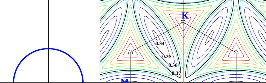
2 transmission of EMW other than conventional approach by using materials with zero-index or zero-average-index. In physics, a wavefront is the locus of points having the same phase and EMW s propagation in media always undergoes phase shift with the wavefront perpendicular to the direction of energy flow. A plane wave traveling in arbitrary direction can be described as E r ) Acos( k r t ), (1) ( 0 with the complex amplitude denoted by ~ E ( r) Aexp[ i( k r 0 )], (2) here A is wave amplitude, k is wave vector pointing to the direction of phase velocity ph with the magnitude of k =2 /, is the wavelength, and r is position vector, 0 is initial phase. In spatial domain, the phase shift between two different positions is determined by the spatial phase factor k r. If the origin of coordinate system is defined on the propagation path, the position vector r points to the direction of energy flow (i.e. the direction of group velocity gr ). When EMW travelling in a conventional material with an ordinary refractive index, i.e. the right-handed (RH) material, the wavefronts travel away from the source with k gr > 0 and gain a positive relative phase. In a left-handed (LH) material, however, the wavefronts travel toward the source with k gr < 0 and accumulate a negative relative phase. Regardless of the propagation mode, the energy flow essentially remains away from the source along the transmission direction. Supposing the condition of k gr =0 is satisfied, the wave vector k pointing to the normal of wavefront is perpendicular to the energy flow with the planar phase fronts extending along the transmission direction, which means that the spatial phase is constant along the energy flow, in other words, zero phase delay of EMW propagation can be realized with the method of wavefront modulation to satisfy the condition of k r =0. On the contrary, in conventional EMW propagation, it is difficult to dramatically modulate wavefronts parallel to the energy flow in homogeneous materials. Photonic crystals [19, 20] are artificial materials with spatially periodical dielectric functions, which can be used to engineer the optical and electromagnetic properties through the geometry of their unit cells. The tailored diffraction gives rise to distinct optical phenomena, such as high-reflecting omni-directional mirrors [21], low-loss-waveguiding [22], super lens [23] and effective negative refraction [24, 25]. In contrast to strong resonance mechanism in metamaterials, the hypernormal optical phenomena of PhC are based on the special dispersion relations of photonic bands with the smaller loss than the former. The method of wavevector diagram is generally used to study the properties of beam propagation in PhCs, in which the k-conservation rule is generalized to satisfy the boundary condition at the interface of PhC with k = /csin inc, and the propagation direction of refracted wave is oriented to the group velocity vector gr = k which is normal to the equal frequency contour (EFC). Due to the large design flexibility of PhC, the EFCs of PhC dominated by the photonic band structure usually present some peculiar shape at certain frequencies to make the propagation direction of refracted wave not parallel to the wave vector, and then
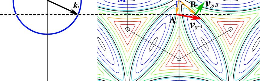
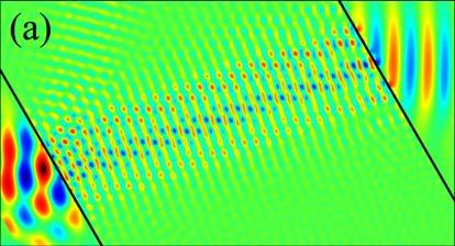
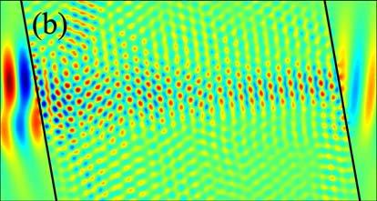
3 induce various transmission phenomena with special optical properties. Hence, PhC can be one optimum candidate for wavefront modulation to achieve zero phase delay of EMW propagation. As an example, a two-dimensional (2D) triangular lattice PhC is proposed in this work to study this novel effect. This PhC slab is composed of low-lossy dielectric rods with r =10 closely packed in air with a center-to-center separation of a (a is the lattice constant), as shown in Fig. 1(a). By utilizing the plane-wave expansion method, we calculate the lowest four bands for TM polarization with electric field E parallel to the dielectric rods as shown in Fig. 1(b) with the normalized frequency of a/λ, where the inset represents the first Brillouin zone of this triangular PhC with three high-symmetry lattice points, and the point Г is the Brillouin zone center. Different from the other bands, the fourth band denoted by the red solid line has the more undulations which imply the more complicated optical properties. In order to clearly analyze the wave optics characteristics of this PhC, the EFC plot of the fourth band is calculated and shown in the right part of Fig. 2 with the highlighted black bold EFCs at the frequency of a/λ, which look like six leaves gathering around the center point. Supposing the source plane wave is incident from air with the incident angle of inc =30 upon the interface between air and the PhC slab with the surfaces along the K direction, the corresponding wave vector diagram is illustrated Fig. 2, where the blue circle represents the air EFC of = a/λ, the black arrow denotes the incident wave vector k i in air, the orange arrows stand for refractive wave vectors k r which are always perpendicular to the phase front, the dashed line means the conservation of the parallel components of wave vectors which validly intersects the EFC of = a/λ twice at different points A and B, and the red and green arrows demonstrate the group velocity directions of two refracted waves A and B, respectively. By the definition of group velocity gr = k, the group velocity vector is oriented perpendicular to the EFC surface in the frequency-increasing direction. By rigorous theoretical analysis, we found that the group velocity of refracted wave A is perpendicular to its wave vector with k gr = 0, which indicates that the condition of zero phase shift can be satisfied in this case. With the frequency increasing, the surrounding EFCs will intersect at the center point. Numerous calculations show that the condition of k gr = 0 can also be satisfied in other cases, such as the incident EMW of a/λ with inc =10. Numerical simulations have been introduced to demonstrate the predicted analytical results. A continuous Gaussian wave source which can be regarded as a plane wave with the spatial width of 6.5a is located in front of the PhC slab with the thickness of 15 layers. As shown in Fig. 3(a), when the source wave with = 0.374a/λ is incident upon the K surface of this PhC slab with inc =30, the wavefront of refracted beam A is modulated by the periodic structure to recombine in the PhC slab with the parallel wavefronts extending along the propagation direction, whose spatial period is approximately 5.2a in the normal direction. Fig. 3(b) shows the simulation of electric field distribution in the PhC slab with the incident EMW of 0.376a/ at inc =10, whose modulated wavefronts in the PhC are also parallel to the transmission direction with a larger spatial period of about 14a. For general optical
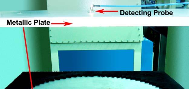
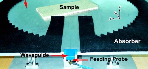
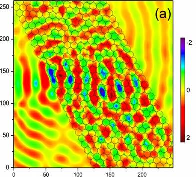
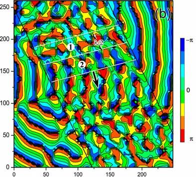
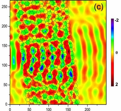
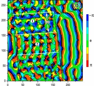
4 systems, phasefront and wavefront are identical as long as the nominal wavefront deviation remains relatively small. To further verify the above mentioned peculiar phenomena experimentally, we design a sample of triangular lattice PhC slab formed by high pure Al 2 O 3 ceramic rods with dielectric constant r =10, relative permeability 1 and loss tangent 0 in this study. The geometric parameters of these Al 2 O 3 ceramic rods are designed as diameter d=10mm, height h=10mm and lattice constant a=10mm, with the same lattice structure as in the simulations above. The sample is placed in a near-field scanning system (microwave planar waveguide) [26], as shown in Fig. 4, where the upper and lower metal plates form the planar waveguide to ensure transverse electromagnetic (TEM) mode invariable between the plates along the z-axis. A rectangular waveguide with the cross-sectional dimensions of 22.86mm 10.16mm is utilized in the lower plate as the X-band waveguide adapter to excite a plane wave with the electric field E perpendicular to the upper and lower conducting plates. In the x-band region (8-12GHz), only the dominant mode of TE 10 can propagate in the waveguide. A detecting probe is mounted in the upper plate to measure the amplitude and phase in the local electric field. The feeding and detecting probes are connected to the output and input ports of the Vector Network Analyzer (VNA) (Agilent ENA5071C). The lower metal plate is carried by the 2D moving stage which can be controlled by a computer to move in x and y directions with a scanning step of 4 mm, so that we can measure EM field distributions within an area. Next, two experiments are conducted to prove the previously mentioned effects of zero phase delay in PhC by modulating the wavefront of transmitted EMW. We show in Fig. 5 the measured electric fields (real part and phase) for each of the cases examined. In the first experiment, the source wave at GHz (i.e. relative frequency of 0.374a/λ) is incident upon the PhC slab with the incident angle of inc =30, both the amplitude and phase internal fields of this PhC sample are measured, allowing us to form an image that can be compared directly with the numerical simulations. In Fig. 5(a), the refracted EMW propagating in the PhC exhibits desired perfect planar wavefronts at the entrance position with the spatial periodic 5.2a, with the further propagation of light in the sample, some wavefront deviations arise from the constructive interference and diffraction of the finite sample area. Since the phase at a given detection location is referenced to the output port of the VNA, it is necessary to scan the phase contrast field in the sample to match up with the analytical simulations. As shown in Fig. 5(b), the negative phase described with the blue area (2) in the PhC slab connects the incident wave and the transmitted wave with the same phase, and the positive phase front is denoted by the red area (1), with the phase contrast mode sliding perpendicular to the energy flow as the black arrow shows. In contrast to the wavefront aberration in Fig. 5(a), the phase fronts in Fig. 5(b) are seen to be considerably more coherent with the simulation results. Due to the nearly invariable phase along the transmission direction, the phase difference between the incident wave and transmitted wave is almost equal to zero just like one continue wave without spatial separation. Further experimental study find that the amplitude and phase distribution of the internal EM field present a dramatic
5 dependence on the frequency and the incident angle. When the source wave of GHz is incident at a small incident angle of 10, the measured electric fields (real part and phase) are demonstrated in Fig. 5(c, d) with a larger spatial period of about 14.1a. The negative and positive phasefronts can be more clearly distinguished by the blue area (1) and red area (2) in phase contrast image of Fig. 5(d). In these cases, the combined effects of wavefront (or phasefront) modulation in the PhC sample agree well with the simulation results, which demonstrate that the method of wavefront modulation is an efficient method to realize zero phase delay of EMW propagation. Compared with the uniform phase distribution in zero-index materials, parallel phasefronts extend along the transmission direction of EMW in the PhC slab, in the spatial domain the phase difference between arbitrary spatial locations in the propagation direction is static and equal to zero, while remaining dynamic in the time domain, thus allowing energy transport. In contrast to the longitudinal direction of the path-averaged zero-index nanofabricated superlattices in Ref.[18], the direction of EMW propagating with zero phase delay in the PhC slab can be easily manipulated by adjusting the incident angle, and the effect of zero phase delay can be realized within a wide scope of incident angle from 28 to 40 in this case. Different from the finite plasma frequency of such materials follow Drude or Drude-Lorenz dispersion models[10, 27, 28], the zero phase delay propagation of EMW based on the wavefront modulation can be realized at different frequencies for a certain PhC as long as the k gr = 0 condition is satisfied. These unique features of this effect may show great impacts on both fundamental physics and optical device applications. In conclusion, we have proposed a new mechanism to realize the zero phase delay for EMW propagation in media based on a novel feature of wavefront modulation of photonic crystals. A triangular lattice PhC can make the wavefront (or phasefront) of EMW parallel to the transmission direction and achieve the zero phase shift between the incident and transmitted EMWs. This effect can also be further extended to the 3D case by modulating the wavefront of EMW to satisfy the condition of k gr = 0. Since the PhC structure can be engineered easily and have large design flexibility, engineered control of phase delay in PhCs may be implemented in chip-scale transmission lines, interferometers with deterministic phase array and dispersion control, and therefore has significant technological potential in phase-insensitive image processing, lumped elements in optoelectronics, information processing. We gratefully acknowledge the financial support from National Natural Science Foundation ( , and ), National High Technology Research and Development Program of China (863 Program) (2012AA030703), China Post-doctoral Research Foundation ( , 2012T50087) and Shandong Natural Science Foundation (ZR2010AM025, ZR2011FQ011).
6 References: [1] S. Yun et al., ACS NANO 6, 4475 (2012). [2] L. Fengming, H. Xueqin, and C. T. Chan, Appl Phys Lett 100, (2012). [3] Y. Xiang et al., Appl Phys B-Lasers O 103, 897 (2011). [4] X. Huang et al., NATURE MATERIALS 10, 582 (2011). [5] R. Polles et al., Opt Express 19, 6149 (2011). [6] F. Bongard, H. Lissek, and J. R. Mosig, Phys Rev B 82, (2010). [7] M. G. Silveirinha, and P. A. Belov, Phys Rev B 77, (2008). [8] F. Zhang et al., J Appl Phys 103, (2008). [9] B. Edwards, A. Alu, M.E. Young, M. Silveirinha, and N. Engheta, Phys Rev Lett 100, (2008). [10] A. Alu, M.G. Silveirinha, A. Salandrino, and N. Engheta, Phys Rev B 75, (2007). [11] I. C. Khoo et al., Opt Lett 31, 2592 (2006). [12] V. C. Nguyen, L. Chen, and K. Halterman, Phys Rev Lett 105, (2010). [13] V. Mocella et al., Phys Rev Lett 102, (2009). [14] H. Zhou et al., J Electromagnet Wave 23, 953 (2009). [15] N. M. Litchinitser et al., Opt Lett 33, 2350 (2008). [16] M. Silveirinha, and N. Engheta, Phys Rev B 75, (2007). [17] M. Silveirinha, and N. Engheta, Phys Rev Lett 97, (2006). [18] S. Kocaman et al., NATURE PHOTONICS 5, 499 (2011). [19] E. Yablonovitch, Phys Rev Lett 58, 2059 (1987). [20] S. John, Phys Rev Lett 58, 2486 (1987). [21] S. D. Hart et al., Science 296, 510 (2002). [22] S. Hughes, L. Ramunno, J.F. Young, and J.E. Sipe, Phys Rev Lett 94, (2005). [23] J. B. Pendry, Phys Rev Lett 85, 3966 (2000). [24] Z. C. Ruan, and S. L. He, Opt Lett 30, 2308 (2005). [25] G. Y. Dong, X. L. Yang, and L. Z. Cai, Opt Express 18, (2010). [26] B. J. Justice et al., Opt Express 14, 8694 (2006). [27] J. M. Hao, W. Yan, and M. Qiu, Appl Phys Lett 96, (2010). [28] J. G. Rivas et al., Opt Express 13, 847 (2005).
7 Figure Caption FIG. 1. (Color online) (a) Schematic of the 2D triangular PhC with Al 2 O 3 ceramic rods closely packed in air; (b) Band diagram of this PhC for TM polarization. FIG. 2. (Color online) EFCs plot of the fourth band with the wave vector diagram at the frequency of 0.374a/λ with inc =30. FIG. 3. (Color online) FDTD simulations of electric field distribution in the PhC slab with the incident beams of (a) =0.374 a/ with inc =30 and (b) =0.376a/ with inc =10. FIG. 4. (Color online) Photograph of the measurement system. FIG. 5. (Color online) The measured spatial mappings of (a) electric field and (b) phase contrast image at GHz with inc =30 ; (c)the electric field and (b) phase contrast image at GHz with inc =10.
 FIG.")
8 (a) Relative Frequency (a ) K (b) FIG. 1
9 FIG. 2
10 FIG. 3
11 FIG. 4
12 FIG. 5
Routing of Deep-Subwavelength Optical Beams and Images without Reflection and Diffraction Using Infinitely Anisotropic Metamaterials
 Peter B. Catrysse * and Shanhui Fan Routing of Deep-Subwavelength Optical Beams and Images without Reflection and Diffraction Using Infinitely Anisotropic Metamaterials Media that are described by extreme
Super-reflection and Cloaking Based on Zero Index Metamaterial
 Super-reflection and Cloaking Based on Zero Index Metamaterial Jiaming Hao, Wei Yan, and Min Qiu Photonics and Microwave ngineering, Royal Institute of Technology (KTH), lectrum 9, 164 4, Kista, Sweden
FDTD Analysis on Optical Confinement Structure with Electromagnetic Metamaterial
 Memoirs of the Faculty of Engineering, Okayama University, Vol. 44, pp. 1-6, January 21 FDTD Analysis on Optical Confinement Structure with Electromagnetic Metamaterial Shinji NAGAI, Ryosuke UMEDA, Kenji
90 degree polarization rotator using a bilayered chiral metamaterial with giant optical activity
 90 degree polarization rotator using a bilayered chiral metamaterial with giant optical activity Yuqian Ye 1 and Sailing He 1,2,* 1 Centre for Optical and Electromagnetic Research, State Key Laboratory
Enhancing and suppressing radiation with some permeability-near-zero structures
 Enhancing and suppressing radiation with some permeability-near-zero structures Yi Jin 1,2 and Sailing He 1,2,3,* 1 Centre for Optical and Electromagnetic Research, State Key Laboratory of Modern Optical
Canalization of Sub-wavelength Images by Electromagnetic Crystals
 Progress In Electromagnetics Research Symposium 2005, Hangzhou, China, August 22-26 37 Canalization of Sub-wavelength Images by Electromagnetic Crystals P. A. Belov 1 and C. R. Simovski 2 1 Queen Mary
3D PRINTING OF ANISOTROPIC METAMATERIALS
 Progress In Electromagnetics Research Letters, Vol. 34, 75 82, 2012 3D PRINTING OF ANISOTROPIC METAMATERIALS C. R. Garcia 1, J. Correa 1, D. Espalin 2, J. H. Barton 1, R. C. Rumpf 1, *, R. Wicker 2, and
A Novel Design of Photonic Crystal Lens Based on Negative Refractive Index
 PIERS ONLINE, VOL. 4, NO. 2, 2008 296 A Novel Design of Photonic Crystal Lens Based on Negative Refractive Index S. Haxha 1 and F. AbdelMalek 2 1 Photonics Group, Department of Electronics, University
Infrared carpet cloak designed with uniform silicon grating structure
 Infrared carpet cloak designed with uniform silicon grating structure Xiaofei Xu, Yijun Feng, Yu Hao, Juming Zhao, Tian Jiang Department of Electronic Science and Engineering, Nanjing Univerisity, Nanjing,
Electromagnetic Absorption by Metamaterial Grating System
 PIERS ONLINE, VOL. 4, NO. 1, 2008 91 Electromagnetic Absorption by Metamaterial Grating System Xiaobing Cai and Gengkai Hu School of Science, Beijing Institute of Technology, Beijing 100081, China Abstract
Nonlinear Metamaterial Composite Structure with Tunable Tunneling Frequency
 Progress In Electromagnetics Research Letters, Vol. 71, 91 96, 2017 Nonlinear Metamaterial Composite Structure with Tunable Tunneling Frequency Tuanhui Feng *,HongpeiHan,LiminWang,andFeiYang Abstract A
Design of a Multi-Mode Interference Crossing Structure for Three Periodic Dielectric Waveguides
 Progress In Electromagnetics Research Letters, Vol. 75, 47 52, 2018 Design of a Multi-Mode Interference Crossing Structure for Three Periodic Dielectric Waveguides Haibin Chen 1, Zhongjiao He 2,andWeiWang
Self-collimating polarization beam splitter based on photonic crystal Mach Zehnder interferometer
 Xu et al. Vol. 27, No. 7/July 2010/J. Opt. Soc. Am. B 1359 Self-collimating polarization beam splitter based on photonic crystal Mach Zehnder interferometer Yi Xu, Shun Wang, Sheng Lan, Xu-Sheng Lin, Qi
Directive Emission Obtained by Mu and Epsilon-Near-Zero Metamaterials
 124 J. YANG, M. HUANG, J. PENG, DIRECTIVE EMISSION OBTAINED BY MU AND EPSILON-NEAR-ZERO METAMATERIALS Directive Emission Obtained by Mu and Epsilon-Near-Zero Metamaterials Jing-jing YANG.1,2, Ming HUANG
Author(s) Tamayama, Y; Nakanishi, T; Sugiyama. Citation PHYSICAL REVIEW B (2006), 73(19)
 Tamayama, Y; Nakanishi, T; Sugiyama. Citation PHYSICAL REVIEW B (2006), 73(19)") Observation of Brewster's effect fo Titleelectromagnetic waves in metamateri theory Author(s) Tamayama, Y; Nakanishi, T; Sugiyama Citation PHYSICAL REVIEW B (2006), 73(19) Issue Date 2006-05 URL http://hdl.handle.net/2433/39884
Observation of Brewster's effect fo Titleelectromagnetic waves in metamateri theory Author(s) Tamayama, Y; Nakanishi, T; Sugiyama Citation PHYSICAL REVIEW B (2006), 73(19) Issue Date 2006-05 URL http://hdl.handle.net/2433/39884
Homogenous Optic-Null Medium Performs as Optical Surface Transformation
 Progress In Electromagnetics Research, Vol. 151, 169 173, 2015 Homogenous Optic-Null Medium Performs as Optical Surface Transformation Fei Sun 1 and Sailing He1, 2, * Abstract An optical surface transformation
Overview. 1. What range of ε eff, µ eff parameter space is accessible to simple metamaterial geometries? ``
 MURI-Transformational Electromagnetics Innovative use of Metamaterials in Confining, Controlling, and Radiating Intense Microwave Pulses University of New Mexico August 21, 2012 Engineering Dispersive
Research on the Wide-angle and Broadband 2D Photonic Crystal Polarization Splitter
 Progress In Electromagnetics Research Symposium 2005, Hangzhou, China, August 22-26 551 Research on the Wide-angle and Broadband 2D Photonic Crystal Polarization Splitter Y. Y. Li, P. F. Gu, M. Y. Li,
Left-handed materials: Transfer matrix method studies
 Left-handed materials: Transfer matrix method studies Peter Markos and C. M. Soukoulis Outline of Talk What are Metamaterials? An Example: Left-handed Materials Results of the transfer matrix method Negative
Modelling and design of complete photonic band gaps in two-dimensional photonic crystals
 PRAMANA c Indian Academy of Sciences Vol. 70, No. 1 journal of January 2008 physics pp. 153 161 Modelling and design of complete photonic band gaps in two-dimensional photonic crystals YOGITA KALRA and
Refraction and rightness in photonic crystals
 Refraction and rightness in photonic crystals R. Gajić 1,2, R. Meisels 2, F. Kuchar 2, K. Hingerl 3 1 Institute of Physics, P.O.Box 68, 11080, Belgrade, Serbia 2 Institute of Physics, University of Leoben,
arxiv: v2 [cond-mat.other] 20 Nov 2008
![arxiv: v2 [cond-mat.other] 20 Nov 2008](/thumbs/76/73207519.jpg "arxiv: v2 [cond-mat.other] 20 Nov 2008") arxiv:8.2666v2 [cond-mat.other] 2 Nov 28 Subwavelength internal imaging by means of the wire medium Yan Zhao, Pavel Belov and Yang Hao School of Electronic Engineering and Computer Science, Queen Mary,
arxiv:8.2666v2 [cond-mat.other] 2 Nov 28 Subwavelength internal imaging by means of the wire medium Yan Zhao, Pavel Belov and Yang Hao School of Electronic Engineering and Computer Science, Queen Mary,
Comparison Study of the Band-gap Structure of a 1D-Photonic Crystal by Using TMM and FDTD Analyses
 Journal of the Korean Physical Society, Vol. 58, No. 4, April 2011, pp. 1014 1020 Comparison Study of the Band-gap Structure of a 1D-Photonic Crystal by Using TMM and FDTD Analyses Jian-Bo Chen, Yan Shen,
A COMPACT POLARIZATION BEAM SPLITTER BASED ON A MULTIMODE PHOTONIC CRYSTAL WAVEGUIDE WITH AN INTERNAL PHOTONIC CRYSTAL SECTION
 Progress In Electromagnetics Research, PIER 103, 393 401, 2010 A COMPACT POLARIZATION BEAM SPLITTER BASED ON A MULTIMODE PHOTONIC CRYSTAL WAVEGUIDE WITH AN INTERNAL PHOTONIC CRYSTAL SECTION Y. C. Shi Centre
Optical anisotropic metamaterials: Negative refraction and focusing
 Optical anisotropic metamaterials: Negative refraction and focusing Anan Fang, 1 Thomas Koschny, 1, and Costas M. Soukoulis 1,, * 1 Department of Physics and Astronomy and Ames Laboratory, Iowa State University,
arxiv: v1 [physics.optics] 10 Apr 2008
![arxiv: v1 [physics.optics] 10 Apr 2008](/thumbs/92/111032309.jpg "arxiv: v1 [physics.optics] 10 Apr 2008") Pendellösung effect in photonic crystals arxiv:0804.1701v1 [physics.optics] 10 Apr 2008 S. Savo 1, E. Di Gennaro 1, C. Miletto 1, A. Andreone 1, P. Dardano 2, L. Moretti 2,3, V. Mocella 2 1 CNISM and Department
Pendellösung effect in photonic crystals arxiv:0804.1701v1 [physics.optics] 10 Apr 2008 S. Savo 1, E. Di Gennaro 1, C. Miletto 1, A. Andreone 1, P. Dardano 2, L. Moretti 2,3, V. Mocella 2 1 CNISM and Department
CHAPTER 9 ELECTROMAGNETIC WAVES
 CHAPTER 9 ELECTROMAGNETIC WAVES Outlines 1. Waves in one dimension 2. Electromagnetic Waves in Vacuum 3. Electromagnetic waves in Matter 4. Absorption and Dispersion 5. Guided Waves 2 Skip 9.1.1 and 9.1.2
Citation for published version (APA): Shen, C. (2006). Wave Propagation through Photonic Crystal Slabs: Imaging and Localization. [S.l.]: s.n.
![Citation for published version (APA): Shen, C. (2006). Wave Propagation through Photonic Crystal Slabs: Imaging and Localization. [S.l.]: s.n.](/thumbs/95/124821981.jpg "Citation for published version (APA): Shen, C. (2006). Wave Propagation through Photonic Crystal Slabs: Imaging and Localization. [S.l.]: s.n.") University of Groningen Wave Propagation through Photonic Crystal Slabs Shen, Chuanjian IMPORTANT NOTE: You are advised to consult the publisher's version (publisher's PDF) if you wish to cite from it.
University of Groningen Wave Propagation through Photonic Crystal Slabs Shen, Chuanjian IMPORTANT NOTE: You are advised to consult the publisher's version (publisher's PDF) if you wish to cite from it.
Demonstration of Near-Infrared Negative-Index Materials
 Demonstration of Near-Infrared Negative-Index Materials Shuang Zhang 1, Wenjun Fan 1, N. C. Panoiu 2, K. J. Malloy 1, R. M. Osgood 2 and S. R. J. Brueck 2 1. Center for High Technology Materials and Department
Electromagnetic Metamaterials
 Electromagnetic Metamaterials Dr. Alkim Akyurtlu Center for Electromagnetic Materials and Optical Systems University of Massachusetts Lowell September 19, 2006 Objective Outline Background on Metamaterials
A Broadband Flexible Metamaterial Absorber Based on Double Resonance
 Progress In Electromagnetics Research Letters, Vol. 46, 73 78, 2014 A Broadband Flexible Metamaterial Absorber Based on Double Resonance ong-min Lee* Abstract We present a broadband microwave metamaterial
Sub-wavelength electromagnetic structures
 Sub-wavelength electromagnetic structures Shanhui Fan, Z. Ruan, L. Verselegers, P. Catrysse, Z. Yu, J. Shin, J. T. Shen, G. Veronis Ginzton Laboratory, Stanford University http://www.stanford.edu/group/fan
Light Manipulation by Metamaterials
 Light Manipulation by Metamaterials W. J. Sun, S. Y. Xiao, Q. He*, L. Zhou Physics Department, Fudan University, Shanghai 200433, China *Speaker: qionghe@fudan.edu.cn 2011/2/19 Outline Background of metamaterials
An efficient way to reduce losses of left-handed metamaterials
 An efficient way to reduce losses of left-handed metamaterials Jiangfeng Zhou 1,2,, Thomas Koschny 1,3 and Costas M. Soukoulis 1,3 1 Ames Laboratory and Department of Physics and Astronomy,Iowa State University,
Tooth-shaped plasmonic waveguide filters with nanometeric. sizes
 Tooth-shaped plasmonic waveguide filters with nanometeric sizes Xian-Shi LIN and Xu-Guang HUANG * Laboratory of Photonic Information Technology, South China Normal University, Guangzhou, 510006, China
THE PROPAGATION AND CUTOFF FREQUENCIES OF THE RECTANGULAR METALLIC WAVEGUIDE PAR- TIALLY FILLED WITH METAMATERIAL MULTILAYER SLABS
 Progress In Electromagnetics Research M, Vol. 9, 35 40, 2009 THE PROPAGATION AND CUTOFF FREQUENCIES OF THE RECTANGULAR METALLIC WAVEGUIDE PAR- TIALLY FILLED WITH METAMATERIAL MULTILAYER SLABS D. Zhang
Workshop on New Materials for Renewable Energy
 2286-6 Workshop on New Materials for Renewable Energy 31 October - 11 November 201 Metamaterials: Past, Present, and Future Nonlinear Physics Centre Research School of Physics and Engineering The Australian
Band structure and transmission of 3D chiral sonic crystals
 Band structure and transmission of 3D chiral sonic crystals R. Pico, V. Romero-Garcia, V. Sanchez-Morcillo, A. Cebrecos and L.M. Garcia-Raffi Universidad Politecnica de Valencia, Paranimf 1, 46730 Gandia,
Directive Emission Obtained by Coordinate Transformation
 Directive Emission Obtained by Coordinate Transformation Jingjing Zhang 1, Yu Luo 1, Hongsheng Chen 1 2*, Lixin Ran 1, Bae-Ian Wu 2, and Jin Au Kong 1 2 1 The Electromagnetics Academy at Zhejiang University,
EPSILON-NEAR-ZERO (ENZ) AND MU-NEAR-ZERO (MNZ) MATERIALS
 AND MU-NEAR-ZERO (MNZ) MATERIALS") EPSILON-NEAR-ZERO (ENZ) AND MU-NEAR-ZERO (MNZ) MATERIALS SARAH NAHAR CHOWDHURY PURDUE UNIVERSITY 1 Basics Design ENZ Materials Lumped circuit elements Basics Decoupling Direction emission Tunneling Basics
EPSILON-NEAR-ZERO (ENZ) AND MU-NEAR-ZERO (MNZ) MATERIALS SARAH NAHAR CHOWDHURY PURDUE UNIVERSITY 1 Basics Design ENZ Materials Lumped circuit elements Basics Decoupling Direction emission Tunneling Basics
Design and Characterization of a Dual-Band Metamaterial Absorber Based on Destructive Interferences
 Progress In Electromagnetics Research C, Vol. 47, 95, 24 Design and Characterization of a Dual-Band Metamaterial Absorber Based on Destructive Interferences Saeid Jamilan, *, Mohammad N. Azarmanesh, and
Plasmonic metamaterial cloaking at optical frequencies
 Plasmonic metamaterial cloaking at optical frequencies F. Bilotti *, S. Tricarico, and L. Vegni Department of Applied Electronics, University Roma Tre Via della Vasca Navale 84, Rome 146, ITALY * Corresponding
Concealing arbitrary objects remotely with multi-folded transformation optics
 Concealing arbitrary objects remotely with multi-folded transformation optics B. Zheng 1, 2, 3, H. A. Madni 1, 2, 3, R. Hao 2, X. Zhang 2, X. Liu 1, E. Li 2* 1, 2, 3* and H. Chen 1 State Key Laboratory
Cloaking The Road to Realization
 Cloaking The Road to Realization by Reuven Shavit Electrical and Computer Engineering Department Ben-Gurion University of the Negev 1 Outline Introduction Transformation Optics Laplace s Equation- Transformation
Two-dimensional Cross Embedded Metamaterials
 PIERS ONLINE, VOL. 3, NO. 3, 7 4 Two-dimensional Cross Embedded Metamaterials J. Zhang,, H. Chen,, L. Ran,, Y. Luo,, and J. A. Kong,3 The Electromagentics Academy at Zhejiang University, Zhejiang University
Supporting Information
 Supporting Information Light emission near a gradient metasurface Leonard C. Kogos and Roberto Paiella Department of Electrical and Computer Engineering and Photonics Center, Boston University, Boston,
SUPPLEMENTARY INFORMATION
 SUPPLEMENTARY INFORMATION Supplementary Information I. Schematic representation of the zero- n superlattices Schematic representation of a superlattice with 3 superperiods is shown in Fig. S1. The superlattice
Theoretical study of subwavelength imaging by. acoustic metamaterial slabs
 Theoretical study of subwavelength imaging by acoustic metamaterial slabs Ke Deng,2, Yiqun Ding, Zhaojian He, Heping Zhao 2, Jing Shi, and Zhengyou Liu,a) Key Lab of Acoustic and Photonic materials and
Chapter 5. Effects of Photonic Crystal Band Gap on Rotation and Deformation of Hollow Te Rods in Triangular Lattice
 Chapter 5 Effects of Photonic Crystal Band Gap on Rotation and Deformation of Hollow Te Rods in Triangular Lattice In chapter 3 and 4, we have demonstrated that the deformed rods, rotational rods and perturbation
Citation for published version (APA): Shen, C. (2006). Wave Propagation through Photonic Crystal Slabs: Imaging and Localization. [S.l.]: s.n.
![Citation for published version (APA): Shen, C. (2006). Wave Propagation through Photonic Crystal Slabs: Imaging and Localization. [S.l.]: s.n.](/thumbs/95/124821987.jpg "Citation for published version (APA): Shen, C. (2006). Wave Propagation through Photonic Crystal Slabs: Imaging and Localization. [S.l.]: s.n.") University of Groningen Wave Propagation through Photonic Crystal Slabs Shen, Chuanjian IMPORTANT NOTE: You are advised to consult the publisher's version (publisher's PDF) if you wish to cite from it.
University of Groningen Wave Propagation through Photonic Crystal Slabs Shen, Chuanjian IMPORTANT NOTE: You are advised to consult the publisher's version (publisher's PDF) if you wish to cite from it.
Flute-Model Acoustic Metamaterials with Simultaneously. Negative Bulk Modulus and Mass Density
 Flute-Model Acoustic Metamaterials with Simultaneously Negative Bulk Modulus and Mass Density H. C. Zeng, C. R. Luo, H. J. Chen, S. L. Zhai and X. P. Zhao * Smart Materials Laboratory, Department of Applied
Study of Propagating Modes and Reflectivity in Bragg Filters with AlxGa1-xN/GaN Material Composition
 Study of Propagating Modes and Reflectivity in Bragg Filters with AlxGa1-xN/GaN Material Composition Sourangsu Banerji Department of Electronics & Communication Engineering, RCC Institute of Information
Transmission Lines. Plane wave propagating in air Y unguided wave propagation. Transmission lines / waveguides Y. guided wave propagation
 Transmission Lines Transmission lines and waveguides may be defined as devices used to guide energy from one point to another (from a source to a load). Transmission lines can consist of a set of conductors,
Negative epsilon medium based optical fiber for transmission around UV and visible region
 I J C T A, 9(8), 2016, pp. 3581-3587 International Science Press Negative epsilon medium based optical fiber for transmission around UV and visible region R. Yamuna Devi*, D. Shanmuga Sundar** and A. Sivanantha
Theoretical studies on the transmission and reflection properties of metallic planar fractals
 INSTITUTE OF PHYSICS PUBLISHING JOURNAL OF PHYSICS D: APPLIED PHYSICS J. Phys. D: Appl. Phys. 37 (2004) 368 373 PII: S0022-3727(04)63919-2 Theoretical studies on the transmission and reflection properties
Acoustic guiding and subwavelength imaging with sharp bending by sonic crystal
 Acoustic guiding and subwavelength imaging with sharp bending by sonic crystal Bo Li, Ke Deng *, and Heping Zhao Department of Physics, Jishou University, Jishou 46, Hunan, hina A sharp bending scheme
PHYSICAL REVIEW B 71,
 Coupling of electromagnetic waves and superlattice vibrations in a piezomagnetic superlattice: Creation of a polariton through the piezomagnetic effect H. Liu, S. N. Zhu, Z. G. Dong, Y. Y. Zhu, Y. F. Chen,
Evanescent modes stored in cavity resonators with backward-wave slabs
 arxiv:cond-mat/0212392v1 17 Dec 2002 Evanescent modes stored in cavity resonators with backward-wave slabs S.A. Tretyakov, S.I. Maslovski, I.S. Nefedov, M.K. Kärkkäinen Radio Laboratory, Helsinki University
Progress In Electromagnetics Research, PIER 97, , 2009
 Progress In Electromagnetics Research, PIER 97, 407 416, 2009 PRACTICAL LIMITATIONS OF AN INVISIBILITY CLOAK B. L. Zhang Research Laboratory of Electronics Massachusetts Institute of Technology MA 02139,
Electromagnetic Theory for Microwaves and Optoelectronics
 Keqian Zhang Dejie Li Electromagnetic Theory for Microwaves and Optoelectronics Second Edition With 280 Figures and 13 Tables 4u Springer Basic Electromagnetic Theory 1 1.1 Maxwell's Equations 1 1.1.1
Spherical cloaking with homogeneous isotropic multilayered structures
 Spherical cloaking with homogeneous isotropic multilayered structures The MIT Faculty has made this article openly available. Please share how this access benefits you. Your story matters. Citation As
File Name: Supplementary Information Description: Supplementary Figures, Supplementary Table, Supplementary Notes and Supplementary References
 Description of Supplementary Files File Name: Supplementary Information Description: Supplementary Figures, Supplementary Table, Supplementary Notes and Supplementary References Supplementary Figure 1.
Electromagnetic Metamaterials
 Photonic Bandgap and Electromagnetic Metamaterials Andrew Kirk andrew.kirk@mcgill.ca ca Department of Electrical and Computer Engineering McGill Institute for Advanced Materials A Kirk 11/24/2008 Photonic
Highly Directive Radiation and Negative Refraction Using Photonic Crystals
 Laser Physics, Vol. 5, No., 5, pp. 7 4. Original Text Copyright 5 by Astro, Ltd. Copyright 5 by MAIK Nauka /Interperiodica (Russia). MODERN TRENDS IN LASER PHYSICS Highly Directive Radiation and Negative
SCATTERING OF ELECTROMAGNETIC WAVES ON METAL NANOPARTICLES. Tomáš Váry, Juraj Chlpík, Peter Markoš
 SCATTERING OF ELECTROMAGNETIC WAVES ON METAL NANOPARTICLES Tomáš Váry, Juraj Chlpík, Peter Markoš ÚJFI, FEI STU, Bratislava E-mail: tomas.vary@stuba.sk Received xx April 2012; accepted xx May 2012. 1.
Effects of Loss Factor on Plane Wave Propagation through a Left-Handed Material Slab
 Vol. 113 (2008) ACTA PHYSICA POLONICA A No. 6 Effects of Loss Factor on Plane Wave Propagation through a Left-Handed Material Slab C. Sabah Electrical and Electronics Engineering Department, University
Left-handed and right-handed metamaterials composed of split ring resonators and strip wires
 Left-handed and right-handed metamaterials composed of split ring resonators and strip wires J. F. Woodley, M. S. Wheeler, and M. Mojahedi Electromagnetics Group, Edward S. Rogers Sr. Department of Electrical
Photonic/Plasmonic Structures from Metallic Nanoparticles in a Glass Matrix
 Excerpt from the Proceedings of the COMSOL Conference 2008 Hannover Photonic/Plasmonic Structures from Metallic Nanoparticles in a Glass Matrix O.Kiriyenko,1, W.Hergert 1, S.Wackerow 1, M.Beleites 1 and
Negative refraction and left-handed behavior in two-dimensional photonic crystals
 Negative refraction and left-handed behavior in two-dimensional photonic crystals S. Foteinopoulou and C. M. Soukoulis Ames Laboratory-USDOE and Department of Physics and Astronomy, Iowa State University,
Polarization control of defect modes in threedimensional woodpile photonic crystals
 Polarization control of defect modes in threedimensional woodpile photonic crystals Michael James Ventura and Min Gu* Centre for Micro-Photonics and Centre for Ultrahigh-bandwidth Devices for Optical Systems,
Inside-out electromagnetic cloaking
 Inside-out electromagnetic cloaking Nina A. Zharova 1,2, Ilya V. Shadrivov 1, and Yuri S. Kivshar 1 1 Nonlinear Physics Center, Research School of Physical Sciences and Engineering, Australian National
Investigation of one-dimensional photonic bandgap structures containing lossy double-negative metamaterials through the Bloch impedance
 Shi et al. Vol. 3, No. 6 / June 23 / J. Opt. Soc. Am. B 473 Investigation of one-dimensional photonic bandgap structures containing lossy double-negative metamaterials through the Bloch impedance Fenghua
Electromagnetic fields and waves
 Electromagnetic fields and waves Maxwell s rainbow Outline Maxwell s equations Plane waves Pulses and group velocity Polarization of light Transmission and reflection at an interface Macroscopic Maxwell
Negative Index of Refraction in Optical Metamaterials
 1 Negative Index of Refraction in Optical Metamaterials V. M. Shalaev, W. Cai, U. Chettiar, H.-K. Yuan, A. K. Sarychev, V. P. Drachev, and A. V. Kildishev School of Electrical and Computer Engineering,
Photon transport enhanced by transverse Anderson localization in disordered superlattices
 Photon transport enhanced by transverse Anderson localization in disordered superlattices P. Hsieh 1,2*, C. Chung 2,3, J. F. McMillan 1, M. Tsai 2,4, M. Lu 5, N. C. Panoiu 6,7, and C. W. Wong 1, 8* 1 Optical
GHz magnetic response of split ring resonators
 Photonics and Nanostructures Fundamentals and Applications 2 (2004) 155 159 www.elsevier.com/locate/photonics GHz magnetic response of split ring resonators Lei Zhang a, G. Tuttle a, C.M. Soukoulis b,
Negative Refraction and Subwavelength Lensing in a Polaritonic Crystal
 Negative Refraction and Subwavelength Lensing in a Polaritonic Crystal X. Wang and K. Kempa Department of Physics, Boston College Chestnut Hill, MA 02467 We show that a two-dimensional polaritonic crystal,
Gradient-index metamaterials and spoof surface plasmonic waveguide
 Gradient-index metamaterials and spoof surface plasmonic waveguide Hui Feng Ma State Key Laboratory of Millimeter Waves Southeast University, Nanjing 210096, China City University of Hong Kong, 11 October
WAVEGUIDES FILLED WITH BILAYERS OF DOUBLE- NEGATIVE (DNG) AND DOUBLE-POSITIVE (DPS) METAMATERIALS
 AND DOUBLE-POSITIVE (DPS) METAMATERIALS") Progress In Electromagnetics Research B, Vol., 75 9, WAVEGUIDES FILLED WITH BILAYERS OF DOUBLE- NEGATIVE (DNG) AND DOUBLE-POSITIVE (DPS) METAMATERIALS E. Cojocaru * Department of Theoretical Physics, Horia
Progress In Electromagnetics Research B, Vol., 75 9, WAVEGUIDES FILLED WITH BILAYERS OF DOUBLE- NEGATIVE (DNG) AND DOUBLE-POSITIVE (DPS) METAMATERIALS E. Cojocaru * Department of Theoretical Physics, Horia
 Johnson, N.P. and Khokhar, A.Z. and Chong, H.M.H. and De La Rue, R.M. and McMeekin, S. (2006) Characterisation at infrared wavelengths of metamaterials formed by thin-film metallic split-ring resonator
arxiv: v1 [physics.optics] 31 Jul 2008
![arxiv: v1 [physics.optics] 31 Jul 2008](/thumbs/92/110605174.jpg "arxiv: v1 [physics.optics] 31 Jul 2008") Superscatterer: Enhancement of scattering with complementary media Tao Yang, Huanyang Chen, Xudong Luo, and Hongru Ma Institute of Theoretical Physics, Shanghai Jiao Tong University, arxiv:0807.5038v1
Superscatterer: Enhancement of scattering with complementary media Tao Yang, Huanyang Chen, Xudong Luo, and Hongru Ma Institute of Theoretical Physics, Shanghai Jiao Tong University, arxiv:0807.5038v1
Spontaneous emission rate of an electric dipole in a general microcavity
 PHYSICAL REVIEW B VOLUME 60, NUMBER 7 15 AUGUST 1999-I Spontaneous emission rate of an electric dipole in a general microcavity Jeong-Ki Hwang, Han-Youl Ryu, and Yong-Hee Lee Department of Physics, Korea
Measurement of the photon dispersion relation in two-dimensional ordered dielectric arrays
 322 J. Opt. Soc. Am. B/Vol. 1, No. 2/February 1993 Robertson et al. Measurement of the photon dispersion relation in two-dimensional ordered dielectric arrays W M. Robertson Institute for Information Technology,
1 The formation and analysis of optical waveguides
 1 The formation and analysis of optical waveguides 1.1 Introduction to optical waveguides Optical waveguides are made from material structures that have a core region which has a higher index of refraction
Negative refractive index in a four-level atomic system
 Negative refractive index in a four-level atomic system Zhang Zhen-Qing( ) a)c)d), Liu Zheng-Dong( ) a)b)c), Zhao Shun-Cai( ) b)c), Zheng Jun( ) c)d), Ji Yan-Fang( ) e), and Liu Nian( ) a)c)d) a) Institute
arxiv: v1 [physics.optics] 19 Jun 2008
![arxiv: v1 [physics.optics] 19 Jun 2008](/thumbs/92/110994891.jpg "arxiv: v1 [physics.optics] 19 Jun 2008") arxiv:0806.3231v1 [physics.optics] 19 Jun 2008 Necessary and sufficient conditions for reflectionless transformation media in an isotropic and homogenous background Wei Yan, Min Yan, Min Qiu Laboratory
arxiv:0806.3231v1 [physics.optics] 19 Jun 2008 Necessary and sufficient conditions for reflectionless transformation media in an isotropic and homogenous background Wei Yan, Min Yan, Min Qiu Laboratory
limitations J. Zhou, E. N. Economou and C. M. Soukoulis
 Mesoscopic Physics in Complex Media, 01011 (010) DOI:10.1051/iesc/010mpcm01011 Owned by the authors, published by EDP Sciences, 010 Optical metamaterials: Possibilities and limitations M. Kafesaki, R.
Wave scattering and splitting by magnetic metamaterials
 Wave scattering and splitting by magnetic metamaterials Alexander B. Kozyrev 1, Chao Qin 1, Ilya V. Shadrivov 2, Yuri S. Kivshar 2, Isaac L. Chuang 3, and Daniel W. van der Weide 1 1 Department of Electrical
PRINCIPLES OF PHYSICAL OPTICS
 PRINCIPLES OF PHYSICAL OPTICS C. A. Bennett University of North Carolina At Asheville WILEY- INTERSCIENCE A JOHN WILEY & SONS, INC., PUBLICATION CONTENTS Preface 1 The Physics of Waves 1 1.1 Introduction
Absorption suppression in photonic crystals
 PHYSICAL REVIEW B 77, 442 28 Absorption suppression in photonic crystals A. Figotin and I. Vitebskiy Department of Mathematics, University of California at Irvine, Irvine, California 92697, USA Received
Angular and polarization properties of a photonic crystal slab mirror
 Angular and polarization properties of a photonic crystal slab mirror Virginie Lousse 1,2, Wonjoo Suh 1, Onur Kilic 1, Sora Kim 1, Olav Solgaard 1, and Shanhui Fan 1 1 Department of Electrical Engineering,
Polarization control and sensing with two-dimensional coupled photonic crystal microcavity arrays. Hatice Altug * and Jelena Vučković
 Polarization control and sensing with two-dimensional coupled photonic crystal microcavity arrays Hatice Altug * and Jelena Vučković Edward L. Ginzton Laboratory, Stanford University, Stanford, CA 94305-4088
A photonic crystal superlattice based on triangular lattice
 A photonic crystal superlattice based on triangular lattice Curtis W. Neff and Christopher J. Summers School of Materials Science and Engineering Georgia Institute of Technology, Atlanta, Georgia 30332-0245
Photonic band gap engineering in 2D photonic crystals
 PRAMANA c Indian Academy of Sciences Vol. 67, No. 6 journal of December 2006 physics pp. 1155 1164 Photonic band gap engineering in 2D photonic crystals YOGITA KALRA and R K SINHA TIFAC-Center of Relevance
Plasmonics. The long wavelength of light ( μm) creates a problem for extending optoelectronics into the nanometer regime.
 creates a problem for extending optoelectronics into the nanometer regime.") Plasmonics The long wavelength of light ( μm) creates a problem for extending optoelectronics into the nanometer regime. A possible way out is the conversion of light into plasmons. They have much shorter
Plasmonics The long wavelength of light ( μm) creates a problem for extending optoelectronics into the nanometer regime. A possible way out is the conversion of light into plasmons. They have much shorter
Translation and Rotation of Transformation Media under Electromagnetic Pulse
 Translation and Rotation of Transformation Media under Electromagnetic Pulse Fei Gao 1, Xihang Shi 1, Xiao Lin 1,3, Hongyi Xu 1, Baile Zhang 1,2, * 1. Division of Physics and Applied Physics, School of
arxiv: v1 [physics.class-ph] 10 Feb 2009
![arxiv: v1 [physics.class-ph] 10 Feb 2009](/thumbs/74/70654766.jpg "arxiv: v1 [physics.class-ph] 10 Feb 2009") Ground-Plane Quasi-Cloaking for Free Space Efthymios Kallos, Christos Argyropoulos, and Yang Hao School of Electronic Engineering and Computer Science, Queen Mary University of London, Mile End Road, London,
Ground-Plane Quasi-Cloaking for Free Space Efthymios Kallos, Christos Argyropoulos, and Yang Hao School of Electronic Engineering and Computer Science, Queen Mary University of London, Mile End Road, London,
arxiv: v1 [physics.optics] 1 May 2011
![arxiv: v1 [physics.optics] 1 May 2011](/thumbs/74/70729533.jpg "arxiv: v1 [physics.optics] 1 May 2011") Robust method to determine the resolution of a superlens by analyzing the near-field image of a two-slit object B. D. F. Casse, W. T. Lu, Y. J. Huang, and S. Sridhar Electronic Materials Research Institute
Robust method to determine the resolution of a superlens by analyzing the near-field image of a two-slit object B. D. F. Casse, W. T. Lu, Y. J. Huang, and S. Sridhar Electronic Materials Research Institute
Route to low-scattering cylindrical cloaks with finite permittivity and permeability
 Route to low-scattering cylindrical cloaks with finite permittivity and permeability The MIT Faculty has made this article openly available. Please share how this access benefits you. Your story matters.
ARTICLE IN PRESS. Available online at Metamaterials xxx (2008) xxx xxx
 xxx xxx") Available online at www.sciencedirect.com Metamaterials xxx (2008) xxx xxx Modal interactions in resonant metamaterial slabs with losses G. Lovat a,, P. Burghignoli b,1, A.B. Yakovlev c,2, G.W. Hanson
Available online at www.sciencedirect.com Metamaterials xxx (2008) xxx xxx Modal interactions in resonant metamaterial slabs with losses G. Lovat a,, P. Burghignoli b,1, A.B. Yakovlev c,2, G.W. Hanson