Field Emission Properties of Single-Walled Carbon Nanotubes with a
|
|
|
- June Holland
- 5 years ago
- Views:
Transcription
1 Field Emission Properties of Single-Walled Carbon Nanotubes with a Variety of Emitter-Morphologies Yosuke SHIRATORI, Koji FURUICHI 1, Suguru NODA, Hisashi SUGIME, Yoshiko TSUJI, Zhengyi ZHANG 2, Shigeo MARUYAMA 2, and Yukio YAMAGUCHI Department of Chemical System Engineering, School of Engineering, The University of Tokyo, Hongo, Bunkyo-ku, Tokyo , Japan 1 DAINIPPON SCREEN MFG. CO., LTD., Tenjinkita 1-1, Teranouchi-agaru 4, Horikawa-dori, Kamigyo-ku, Kyoto , Japan 2 Department of Mechanical Engineering, School of Engineering, The University of Tokyo, Hongo, Bunkyo-ku, Tokyo , Japan * address: y-shiratori@chemsys.t.u-tokyo.ac.jp address: noda@chemsys.t.u-tokyo.ac.jp Field emission properties of single-walled carbon nanotubes (SWNTs), which have been prepared through alcohol catalytic chemical vapor deposition for s, were characterized in a diode configuration. Protrusive bundles at the top surface of samples act selectively as emission sites. The number of emission sites was controlled by emitter morphologies combined with texturing of Si substrates. SWNTs grown on a textured Si 1
2 substrate exhibited a turn-on field as low as 2.4 V/μm at a field emission current density of 1 μa/cm 2. Uniform spatial luminescence (0.5 cm 2 ) from the rear surface of the anode was revealed for SWNTs prepared on the textured Si substrate. Deterioration of field emission properties through repetitive measurements was reduced for the textured samples in comparison with vertically aligned SWNTs and a random network of SWNTs prepared on flat Si substrates. Emitter morphology resulting in improved field emission properties is a crucial factor for the fabrication of SWNT-electron sources. Morphologically controlled SWNTs with promising emitter performances are expected to be practical electron sources. KEYWORDS: single-walled carbon nanotube, field emission, alcohol catalytic chemical vapor deposition, ethanol, textured Si, Raman spectroscopy 2
3 1. Introduction Since the potential of carbon nanotubes (CNTs) as electron sources was demonstrated by Rinzler et al., 1) much effort has been devoted to trial applications of CNTs for field emission displays (FEDs). Several different types of CNTs have been implemented into triode-type FEDs. The Samsung and the Motorola groups reported potential of color-swnt- and -MWNT-FEDs, 2,3) respectively. However the practical performance requirements for CNT-FEDs, e.g. uniformity of emission sites and high extractive ratio (anode current/cathode current) in a triode-configuration, have not achieved levels comparable to the Spindt-type FED. 4) Due to their large tip-curvature and metallic conductivity, excellent field emission properties of CNTs have been demonstrated by numerous groups, however their practical use has not yet been realized. One of the major obstacles to developing CNT-FEDs is the severe conditions, such as high-temperatures required for growth especially for SWNTs. For the cases of low-temperature plasma-enhanced chemical vapor deposition (CVD), ambitious infrastructure is necessary. For the CNT-FED equipped with screen-printed SWNT-emitters, 2) which were fabricated under mild conditions, large cathode-holes result in a reduced hole density compared with the Spindt-type FED, causing an 3
4 inhomogeneous current distribution. The choice of CNTs, suitable as electron emitters, is important. SWNTs typically have diameters ranging from 1 to 2 nm, which enhance an applied electric field. On the other hand they consist of only one rolled graphene sheet and they are therefore more flexible than multi-walled nanotubes (MWNTs). We failed to find any literature reporting the accurate sustainable current per SWNT, however their current-durability is believed to be poorer than those for double-walled carbon nanotubes (DWNTs) and MWNTs. This indicates that the ideal concepts of sustainable emission by thick tubes and low extraction voltage by sharp tip are not mutually achievable. A number of issues are important for future CNT-FED development. (I) A low-temperature and/or short-time growth directly on cathodes through simple and safe processes, (II) a giant tip-enhancement of an applied field and (III) a uniform spacial current distribution, that is, a large number density of emission sites resulting in a mild current per emitter. We focus here on SWNT-emitters prepared using alcohol catalytic CVD (ACCVD). ACCVD, which facilitates a low-temperature synthesis (down to 550 C) of high quality SWNTs through a safe process, was developed by Maruyama et al. 5) Ethanol was thermally decomposed over the Fe/Co catalytic mixture embedded in zeolite 5) and 4
5 the Co-Mo bimetallic catalytic layer dip-coated from a metal acetate solution. 6) Field electron emission (FE) from the SWNTs synthesized by ACCVD was first observed for samples prepared on mesoporous-sio 2 (200 nm)/co-nanoparticles/au-ti(300 nm)/si substrates. 7) The properties obtained for the SWNTs (the turn-on field of 4.2 V/μm at the current density of 10 μa/cm 2 and the current density of 0.5 ma/cm 2 at 5.8 V/μm) are believed to be further improved by controlling the emitter morphology and by optimization of growth conditions. On the other hand, randomly oriented SWNTs, which were synthesized using the CO disproportionation reaction catalyzed by silica-supported Co-Mo bimetal, showed good FE properties due to significant prevention of field-shielding especially for samples with a smaller CNT-bundle size. For this structure the turn-on field was 0.6 V/μm and the current density was 1 ma/cm 2 at 1.8 V/μm. 8) This suggests that the control of emitter morphology through optimization of catalytic layers and of growth conditions is crucial for further studies. ACCVD is suitable for SWNT growth directly and selectively on desired positions. SWNTs synthesized from ethanol, which is catalyzed by self-organized metal nanoparticles prepared by RF-magnetron sputtering of metals of the order of 0.1 nm-average thickness and subsequent reduction, has been actively and systematically studied. 9,10) Prior to application of ACCVD for device fabrication, suitable catalyst 5
6 compositions to promote a rapid growth of high quality SWNTs, and the FE properties of the obtained SWNTs must be systematically studied. In this paper we report field emission properties of SWNT-emitters with different morphologies prepared through ACCVD, which is catalyzed by representative catalytic/supporting layers (Co/Al 2 O 3 (Al)) and discuss their potential for FED-applications. 2. Experimental Methods Conventional silicon wafers were used as substrates. After removal of the oxidized layer by hydrofluoric acid, a catalyst supporting layer (Al 2 O 3 or Al) and a Co catalytic layer were deposited on the substrates by using a conventional RF-sputtering system. In addition to the substrates with a flat Si(100) surface, special substrates with textured surfaces were also prepared by a wet chemical etching in hydrazine hydrate at 80 C. Because the Si(111) surface is more resistant to etching by a strong base, Si pyramids with the (111) side faces are formed on the (100) surface. Sample preparation conditions are specified for all samples in Table 1. After taking the substrates out of the sputtering chamber, reduction of the oxidized top-surface and subsequent ACCVD were carried out in the hot-wall ACCVD chamber consisting of a quartz glass tube entirely heated by a furnace. After the reduction process, ACCVD was performed at 785 C by introducing 6
7 ethanol at 4 kpa for s. Obtained sample-surfaces were observed by a Hitachi S-4700 field emission scanning electron microscope (SEM). Raman spectroscopy was used to evaluate the quality of CNTs at the molecular level. Raman spectroscopy is very powerful since graphite related materials scatter intense peaks at around 1590 cm -1 originating from the in-plane lattice vibrations (G-band) and another peak at around 1350 cm -1 attributed to lattice defects in graphene sheets (D-band). 11) The intensity ratio between both bands (G/D-ratio) is an indicator of the quality of obtained CNTs. Raman spectra were recorded by a CHROMEX 501is spectrometer equipped with an ANDOR Technology DV401-FI CCD system under a backscattering configuration. The samples were excited with an Ar + -laser radiation (488.0 nm), which was focused on sample surfaces through a SEKI TECHNOTRON optical unit and objectives with a magnification of 50 and a numerical aperture of FE currents from the obtained CNT-films were measured 8 times at about Pa under a diode configuration. The bottom surface of samples was grounded. An indium-tin-oxide (ITO) glass and 150 μm-thick glass-slides located above a CNT film were used as an anode and spacers, respectively. Measurement areas were approximately 0.9 cm 2. Voltage was swept by a KEITHLEY 2410 high-voltage source 7
8 meter, which is simultaneously an ammeter. Measurements were remote-controlled by the LabTracer2 software and optional interfaces. I-V data were recorded every 30 ms in a voltage ramp of 200 V/s and automatically loaded into an equipped PC. To evaluate the luminescence uniformity, pulsed voltages (5 ms, 1/2-duty) were applied. Phosphor layers on ITO/glass substrates were prepared by screen-printing of ZnO:Zn powders. 3. Results and Discussion 3.1 Combinations of catalyst / supporting material / substrate CNT growth rate and quality are tunable by varying combinations of catalytic materials supporting materials substrates. If an Al 2 O 3 layer is used as a catalyst supporting layer, a higher growth rate is expected due to efficient incorporation of carbon into catalyst particles via Al 2 O 3 surfaces. 12) However an increased Co-thickness (around 1 nm) in comparison with the case of the Co/SiO 2 /Si system 9) is necessary. In fact, a Co layer with a thickness of ca. 0.1 nm on a SiO 2 /Si substrate transforms into Co nano-particles during annealing and such self-organized particles induce growth of high quality SWNTs. Detail roles of the Al 2 O 3 supporting layer on CNT-growth will be discussed elsewhere. In the present case, the average Co- and Al 2 O 3 -thicknesses are fixed into 1.2 and 10 nm, respectively, which promote growth of relatively high quality 8
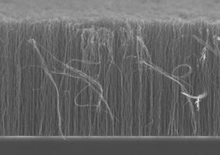
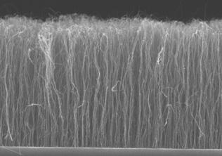
9 CNTs. Here the following points should be noted: (1) discrepancy of growth rates obtained under the same conditions (Table I) may attribute to gaseous hydrodynamics and incubation and so on during ACCVD, which are not severely controlled in this work and (2) the Al 2 O 3 layer as thin as 10 nm, which has a moderate resistance for microcathode applications, acts not only as a catalyst support but also as a resistive layer for stable FE operations in practical triode devices. In order to evaluate the influence of an Al 2 O 3 layer on FE behavior, a representative sample with an Al layer in place of an Al 2 O 3 layer was also characterized. The main roles of an Al layer are also inhibition of Co-diffusion into Si and decomposition of carbon source gas at the oxidized thin layer, but the layer is conductive. 3.2 VA-CNTs and CNT-grass Characterization of CNTs Vertically aligned (VA)-CNTs were prepared on the Co/Al 2 O 3 /Si (Sample A) and Co/Al/Si (Sample B) substrates. A random network of CNTs (CNT-grass) 13) was formed on the Co/Al 2 O 3 /Si substrate (Sample C). Growth conditions including thicknesses of catalytic/supporting layers are summarized in Table I with those for the other CNTs introduced in 3.3. SEM micrographs obtained for VA-CNTs and a CNT-grass 9
10 synthesized by ACCVD are shown in Fig. 1. Surface morphology of the VA-CNTs (Fig. 1(a), right) is grass-like consisted of entangled bundles. On the other hand, in Sample C (Fig. 1(c)), free-standing bundles with heights in μm order are found. Protrusion of specific bundles in as-prepared Sample C is much more pronounced in comparison to the VA-SWNTs (Samples A and B) since the protrusive bundles are not buried in the surrounding SWNT-grass (Fig. 1(c)). In the case of the VA-SWNTs, protrusion of bundles is not so pronounced because they are buried in the thick CNT forest (Fig. 1(a), right). Figure 2 shows representative Raman spectra recorded for Samples A-C. All spectra clearly show radial breathing modes (RBMs) at the low-wavenumber region, indicating the presence of SWNTs. The major peaks marked by triangles correspond to the RBMs of SWNTs with diameters ranging from 0.8 to 1.4 nm, which are estimated from the relationship, d = 248/ω (d:diameter, ω: wavenumber). 5) The peak at around 180 cm -1 ( ), which is a polarized band enhanced for VA-SWNTs, 14) is clearly intensified for Samples A and B. A sharp peak at around 520 cm -1 apparent in Sample C originates from the Si-Si lattice vibration of the Si substrate. The obtained CNTs reveal sharp and split profiles of the G-band and G/D ratios ranging from 6 to 14, which are reasonable profiles for SWNTs. 10
11 3.2.2 Field emission properties of VA-SWNTs and SWNT-grass The current density (J) electric field (E) curves and the Fowler-Nordheim (F-N) plots obtained from the first (red) and third (blue) runs for Samples A-C are shown in Fig. 3. Here J is the current divided by the electrode area. According to the F N theory for electron emission from a metal surface at an applied field E local, the obtained current density J FN (Acm -2 ) is given by eq. (1) 8), J FN = φ ( E ) local φ exp Elocal 1.5, (1) where E local is a local field at an emission site given in Vcm -1 and φ is the work function of an emitter material in ev. Here we assume φ of the present SWNTs is 5 ev, 11) which is a typical value for graphite. The field enhancement factor β (in cm -1 ) is defined in terms of E local = β V, where V is an applied voltage. Equation (1) is transformed as φ Sβ ( ) ( ) V = 1 V + ln β φ ln I, (2) where S is an effective emission area in cm 2. Because the coefficient of 1/V and the last term in eq. (2) are uniquely determined for each emitter structure, the relationship between 1/V and ln(i/v 2 ) should be linear if an anode current originates from field electron emission. β values are estimated from slopes of the relationship. The FE 11
12 parameters obtained for Samples A-C are listed in Table II with those for other samples introduced in 3.3. The values for the first run and the average values for the subsequent runs are shown separately. The data for the second runs are excluded since they show the mixed properties of the first run and the subsequent runs. For the first runs (Fig. 3(a), red), the turn-on fields (E to ), which extract the current density of 1 μa/cm 2, and the current densities at 4 V/μm (J 4.0 ) are smaller and larger than those from the subsequent runs (Fig. 3(a), bule), respectively. Large field enhancement occurs during the first run. The β values calculated from the slopes (s 1 and s 2 in Fig. 3(b)) are listed in Table II; lines 1, 3 and 5. Subsequent runs reveal almost linear F-N plots (shown in blue) and deterioration of FE characteristics (Table II; lines 2, 4 and 6). Samples A (open circle) and B (closed circle) showed similar FE characteristics (Fig. 3, Table II), indicating that we can exclude difference of supporting layers (Al 2 O 3 or Al) from the major factors determining FE properties. The first run F-N characteristic is especially non-linear and comprises two types of relationships (Fig. 3(b)). Possible factors contributing to the non-linearity are (1) adsorbate-enhanced field emission, 15-17) (2) current-induced evaporation (Joule heating), 17-20) (3) stretching of entangled CNTs 18,21) or Y shape splitting of a bundle during voltage sweep, 18) (4) a local density of states (LDOS) at the tips of CNTs, 22-24) (5) effect of space charge caused 12
13 by ionization of residual gases, 21,23-26) and (6) a large resistance between CNTs and a cathode electrode. 17) In the present case, the resistance between SWNTs and the backside of a Si substrate is several to several tens of kω. Since the effect of resistance (Factor (6)) is negligible below several tens of kω, we exclude this effect as the major mechanism of nonlinearity. Exceptionally protrusive bundles in the as-prepared cathodes can enhance the electric field. At 2 3 V/μm in the first run, a higher field enhancement switches on (Fig. 3(b), red). It is difficult to identify the mechanism from the present study, however the effective field at very local protrusions in the first run is variable by field-induced motions of bundles (Factor (3)). Possibly local protrusive emitters in the as-prepared samples rise up by the applied electric field. This finding coincides with the results that the difference in β values below and above 3.0 V/μm for Samples A and B, for which their stems are buried in the forest, is larger than that below and above 2.4 V/μm for Sample C. Protrusive SWNTs causing giant field enhancement are sublimated, subsequently emission sites will be renewed. It is believed that the total achieved current of ca. 0.5 ma in the first run is divided into a small number of emission sites induces evaporation of a SWNT (Factor (2)). Finally the sites, which are subjected to comparable enhanced fields, increase. Here Factor (1), adsorbate-enhanced FE, should 13
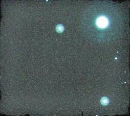
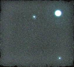
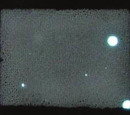
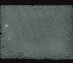
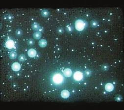
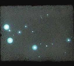
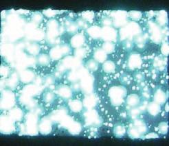
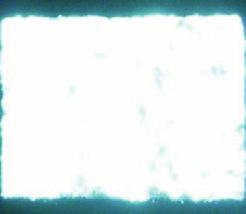
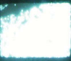
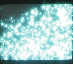
14 also be noted however FE evaluation after atmospheric exposure and subsequent evacuation indicated the effect of initial protrusion in as-prepared samples is more significant for the first measuring runs than the effect of atmospheric adsorbates. In the subsequent measuring runs for Sample C, the E to, J 4.0 and β values (Table II; line 6) are slightly worse than those for Samples A and B (Table II; lines 2 and 4). Figure 4 shows the photographic images of luminescence from the rear surface of the anode at 3.3, 4.1 and 4.8 V/μm (pulse mode) obtained for Samples A, B and C. Highly localized luminescence observed for Samples A and B (Figs. 4(a) and 4(b)) is caused by the limited number of the emission sites; field enhancement occurs only at the tips of local protrusive bundles but not at the top-surface of VA-SWNTs due to field screening effect. 26) Luminescent spots are more widely spread for Sample C than the others. The larger number of luminescent spots for Sample C than Samples A and B corresponds to the larger number of protrusions. However in order to describe screening effect multilevel consideration is necessary. Highly localized emission sites in Samples A and B, which have higher β than that of Sample C, are more screening-free than the sites in Sample C. The fact that screening effect is still observed in Sample C agrees with the emitter morphology observed by SEM (Fig. 1(c)), which induces the screening effect (inter-bundle distance < 2 bundle height). 26) 14
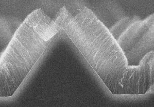
15 Strictly speaking the F-N relationships are not perfectly linear in the subsequent runs for Samples A and B (Fig. 3(b), blue). Inflection points at around 3 V/μm are shown by an arrow in Fig. 3(b). Field emission characteristics transform into the large field enhancement state with a smaller slope at around 3 V/μm. In the present case, it is believed that a local FE and a local large current induce non-linear F-N relationships. In order to reveal the mechanisms, detail studies for Factors (1) (5) causing non-linear F-N relationships are necessary. Field emission properties are determined from (I) primary structure (SWNT, DWNT,, MWNT), (II) secondary structure (bundle shape; height, diameter) and (III) tertiary structure (emitter spacing). The major morphological difference between the top surfaces of VA-SWNTs and CNT-grass is therefore tertiary structure. 3.3 Effect of substrate texturing Characterization of CNTs We controlled the secondary (bundle shape) and tertiary (emitter spacing) structures through texturing of substrates as described in 2. Figure 5 shows SEM micrographs of VA-CNTs and CNT-grass prepared on the textured Co/Al 2 O 3 /Si substrates (Samples D and E). These CNTs have unique structures. Emission sites may 15
16 be CNTs at the apexes of tilted VA-CNT films in Sample D (Fig. 5(a)) and entangled or free-standing bundles at the tips of Si pyramids in Sample E (Fig. 5(b)). In Samples D and E, the number density of the pyramids is approximately /cm 2. Figure 6 shows representative Raman spectra recorded for Samples D and E. The presence of SWNTs in Sample D is supported by the appearance of RBMs in the low-wavenumber region (Fig. 6(a)). Sample E shows an intense peak at around 520 cm -1 originating from the Si-Si lattice vibration of the Si substrate (Fig. 6(b)). A peak at around 300 cm -1 and another intense peak at around 980 cm -1 detected for Sample E are assigned to background scattering from the Si substrate. Major RBMs detected for Samples A-C (Fig. 2) and a specific band featuring VA-SWNTs at around 180 cm -1 ( ) are also found for Sample D (Fig. 6(a)). The presence of RBMs is not obvious for Sample E due to the intense background signal at the low wavenumber region (Fig. 6(b)). However, a large G/D-ratio (= 21) and a sharp band shape of the G-band support the existence of SWNTs Field emission properties of SWNTs prepared on textured substrates In this section, we discuss effects of secondary and tertiary structures on FE properties. Figure 7 shows the J-E curves and the F-N plots obtained from the first (red) 16
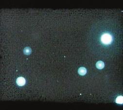
17 and third (blue) runs for Samples D and E. Figure 8 shows the photographic images of luminescence from the rear surface of the anode at 3.3, 4.1 and 4.8 V/μm (pulse mode) for these samples. The FE properties are listed in Table II. Initial protrusions of bundles in the as-grown samples cause giant field enhancement during the first run. Such exceptional protrusions may stretch with increasing applied field and finally evaporate. Compared to for Samples A-C (without texturing), significantly improved FE properties are revealed for Samples D and E in the subsequent runs (Figs. 7, 8 and Table II). For the textured Sample, we exclude the possibility of a lowering of φ originating from amorphous carbon (φ = 1.5 ev) 27), which can be formed on the tips of pyramids by current-induced evaporation. To test this assumption, field emission properties of the textured Si itself (φ = 4.15 ev) 28) and an amorphous carbon film (5 nm) deposited on a textured Si substrate were evaluated and no emission current was detected from either samples up to 5.3 V/μm. In Sample D, protrusive emission sites are located at the edges of VA-SWNTs on the pyramids (as indicated by arrows in Fig. 5(a), right) since a VA-SWNT film only has small number of protrusions at the top surface ( 3.2.2). A number of straggly SWNTs at the edges of the film enhance the applied electric field during the subsequent runs. Moreover in the case that a certain emitter breaks the next emitter becomes active due to 17
18 the high stacking density of aligned SWNTs. As shown in Fig. 8(a), luminescence is observed over the whole area. Lowering of field-screening and an extremely high number of protrusions induce a stable and large area field emission. The inter-pyramid spacing is μm, therefore the screening effect is reduced. Pyramid tips with protrusive bundles selectively become active as emission sites. Single-bundle emitters with diameters of ca. 10 nm (Fig. 5(b)) and inter-bundle spacing of μm in Sample E show the lowest E to, largest J 4.0 (Table II) and the largest number of luminescent spots (Fig. 8(b)). However the β value for the subsequent repetitive runs is still comparable with that for Sample D. Single-bundle emitters entangle or free-stand at the tips of Si pyramids (Fig. 5(b)). These bundles are shorter than straggled bundles at the edges of the VA-SWNT film in Sample D (Fig. 5(a)). Screening-free but short bundles in Sample E settles the β as large as that for Sample D. On the other hand, luminescence image at 3.3 V/μm in Fig. 8(b) shows how the emission sites disperse in comparison with other samples. Assuming that the number density of the pyramids in Sample E is approximately /cm 2 (based on SEM observation) and field enhancement selectively occurs at the tips of pyramids at 4 V/μm, the current density of ca. 1 ma/cm 2 corresponds to 2.5 na per pyramid. This gives us a rough estimate for a tolerable driving current per micro-cathode. Several na per 18
19 micro-cathode is a possible design for SWNT-FEDs. Figure 9 shows linear regressions for the F-N plots obtained from the repetitive measurements (3rd 8th runs) for Samples A and E. It is clear that the field enhancement behavior obtained for Sample E is much more stable in comparison with Sample A. These results indicate that a well separated tertiary structure and a large tip curvature of single-bundle protrusions, which fulfill (1) low driving voltage, (2) large area FE and therefore (3) long life-time, can be prepared though ACCVD by controlling surface morphologies. In addition, up to now it is revealed that a reaction time of 10 s is sufficient to prepare SWNT-emitters under ACCVD conditions used in this work. Consequently morphologically controlled SWNTs prepared through CVD methods have potential performances for FED applications. 4. Conclusions SWNT-emitters were prepared on Co/Al 2 O 3 (Al)/Si substrates through ACCVD, which realizes a reaction time of 10 s to grow a 4 μm-thick SWNT film. Field emission properties of the obtained SWNTs were evaluated under the diode-type configuration. For a textured Si cathode with SWNT-emitters on Si pyramids, the turn-on electric field to extract a current density of 1 μa/cm 2 was 2.4 V/μm, and a current density of
20 ma/cm 2 was recorded at 4 V/μm. Large area luminescence uniformity (0.5 cm 2 ) was also obtained. The study based on the Fowler-Nordheim model showed that field emission properties of SWNTs are tunable by the morphological control of the top-surface. Protrusion of emitters is crucial and the optimization of number density, protrusion length and inter-protrusion distance is necessary for uniform field emission and increased operating life. Texturing of substrates effects a large and selective field enhancement at specific protrusive emitters. Currently, SWNTs prepared from ethanol via a fast and safe process showed field mission characteristics suitable for electron sources. Controllability of SWNT-growth and morphology is advantageous for further study on field emission properties. Acknowledgement We gratefully thank Mr. Kageyasu Kuroki and Mr. Toshio Ohsawa for technical supports and Mr. Takao Kishino for phosphor-printing process. The authors sincerely acknowledge the Ministry of Education, Culture, Sports, Science and Technology (MEXT), Japan for granting a partial financial support: a Grant-in-Aid for Young Scientists (A), ,
21 References 1) A. G. Rinzler, J. H. Hafner, P. Nikolaev, L. Lou, S. G. Kim, D. Tománek, P. Nordlander, D. T. Colbert, and R. E. Smalley: Science 269 (1995) ) J. E. Jung, Y. W. Jin, J. H. Choi, Y. J. Park, T. Y. Ko, D. S. Chung, J. W. Kim, J. E. Jang, S. N. Cha, W. K. Yi, S. H. Cho, M. J. Yoon, C. G. Lee, J. H. You, N. S. Lee, J. B. Yoo, and J. M. Kim: Physica B 323 (2002) 71. 3) B. F. Coll, K. A. Dean, E. Howard, S. V. Johnson, M. R. Johnson, H. Li, D. C. Jordan, L. H. Tisinger, M. Hupp, S. M. Smith, S. R. Young, J. Backer, D. Weston, W. J. Dauksher, Y. Wei, and J. E. Jaskie: EURODISPLAY 05, 2005, p ) S. Itoh, M. Tanaka, and T. Tonegawa: J. Vac. Sci. Technol. B 22 (2004) ) S. Maruyama, R. Kojima, Y. Miyauchi, S. Chiashi, and M. Kohno: Chem. Phys. Lett. 360 (2002) ) Y. Murakami, S. Chiashi, Y. Miyauchi, M. Hu, M. Ogura, T. Okubo, and S. Maruyama: Chem. Phys. Lett. 385 (2004) ) M. Tamura, Y. Kemmochi, Y. Murakami, N. Chino, M. Ogura, S. P. Naik, M. Takai, Y. Tsuji, S. Maruyama, and T. Okubo: Appl. Phys. A 84 (2006) ) L. Zhang, L. Balzano, and D. E. Resasco: J. Phys. Chem. B 109 (2005) ) S. Noda, Y. Tsuji, Y. Murakami, and S. Maruyama: Appl. Phys. Lett. 86 (2005) 21
22 ) S. Noda, H. Sugime, T. Ohsawa, Y. Tsuji, S. Chiashi, Y. Murakami, and S. Maruyama: Carbon 44 (2006) ) M. Sveningsson, R.-E. Morjan, O.A. Nerushev, Y. Sato, J. Bäckström, E.E.B. Campbell, and F. Rohmund: Appl. Phys. A 73 (2001) ) S. Noda, K. Hasegawa, H. Sugime, K. Kakehi, Z. Zhang, S. Maruyama, and Y. Yamaguchi: Jpn. J. Appl. Phys. 46 (2007) L ) L. Zhang, Y. Tan, and D. E. Resasco: Chem. Phys. Lett. 422 (2006) ) Y. Murakami, S. Chiashi, E. Einarsson, and S. Maruyama: Phys. Rev. B 71 (2005) ) K. A. Dean and B. R. Chalamala: Appl. Phys. Lett. 76 (2000) ) Y. C. Choi, Y. M. Shin, D. J. Bae, S. C. Lim, Y. H. Lee, and B. S. Lee: Diamond Relat. Mater. 10 (2001) ) J.-M. Bonard, C. Klinke, K. A. Dean, and B. F. Coll: Phys. Rev. B 67 (2003) ) Y. Saito, K. Seko, and J. Kinoshita: Diamond Relat. Mater. 14 (2005) ) Y. Wei, C. Xie, K. A. Dean, and B. F. Coll: Appl. Phys. Lett. 79 (2001) ) C. Jin, J. Wang, M. Wang, J. Su, L.-M. Peng: Carbon 43 (2005)
23 21) H. Sato, K. Hata, H. Miyake, K. Hiramatsu, and Y. Saito: J. Vac. Sci. Technol. B 23 (2005) ) D. L. Carroll, P. Redlich, P. M. Ajayan, J. C. Charlier, X. Blase, A. De Vita, and R. Car: Phys. Rev. Lett. 78 (1997) ) J.-M. Bonard, J.-P. Salvetat, T. Stöckli, W. A. de Heer, L. Forró, and A. Châtelain: Appl. Phys. Lett. 73 (1998) ) W. B. Choi, Y. H. Lee, N. S. Lee, J. H. Kang, S. H. Park, H. Y. Kim, D. S. Chung, S. M. Lee, S. M. Lee, S. Y. Chung, and J. M. Kim: Jpn. J. Appl. Phys. 39 (2000) ) N. S. Xu, Y. Chen, S. Z. Deng, J. Chen, X. C. Ma, and E. G. Wang: J. Phys. D: Appl. Phys. 34 (2001) ) N. S. Xu and S. E. Huq: Mater. Sci. Eng. R 48 (2005) ) V. M. Anishchik, V. V. Uglov, A. K. Kuleshov, A. R. Filipp, D. P. Rusalsky, M. V. Astashynskaya, M. P. Samtsov, T. A. Kuznetsova, F. Thiery, and Y. Pauleau: Thin Solid Films 482 (2005) ) C. Li, G. Fang, S. Sheng, Z. Chen, J. Wang, S. Ma, and X. Zhao: Physica E 30 (2005)
24 Captions for figures Fig. 1. SEM micrographs of (a, b) VA-CNTs on the Co/Al 2 O 3 /Si (Sample A) and Co/Al/Si (Sample B) substrates and (c) CNT-grass on the Co/Al/Si substrate (Sample C). Enlarged image of the top surface of Sample A is shown in (a)-right. Protrusive bundles in Sample C are indicated by arrows (c). Fig. 2. Raman spectra of (a, b) VA-CNTs on the Co/Al 2 O 3 /Si (Sample A) and Co/Al/Si (Sample B) substrates and (c) CNT-grass on the Co/Al/Si substrate (Sample C). Enlarged spectra of the low wavenumber region are indicated in the insets. Major RBMs are marked by triangles and auxiliary lines: ( ) vertically aligned SWNTs and ( ) others. Fig. 3. (a) J-E curves and (b) F-N plots obtained from the first (red) and the third (blue) measuring runs under the dc-voltage sweep mode for Samples A ( ), B ( ) and C ( ). F-N plots for the first runs are composed of two linear relationships with the slopes s 1 (< 3 μm) and s 2 (> 3 μm). Changes of the slopes observed for Samples A and B at around 3 V/μm during the third run are indicated by an arrow. 24
25 Fig. 4. Pictures of luminescence from the rear surface of the anode at 3.3, 4.1 and 4.8 V/μm under the pulse driving mode (5 ms, 1/2-duty) and cross-sectional SEM micrographs; (a) Sample A, (b) Sample B and (c) Sample C. Fig. 5. SEM micrographs of (a) VA-CNTs on Sample D (left: top view, right: cross sectional view) and (b) CNT-grass on Sample E (left: entangled bundle, right: vertically standing bundle) prepared on the textured Co/Al 2 O 3 /Si substrates. Protrusions are indicated by arrows. Inset in (b) is an enlarged image of the bundle. Fig. 6. Raman spectra of (a) VA-CNTs (Sample D) and (b) CNT-grass (Sample E) prepared on the textured Co/Al 2 O 3 /Si substrates. Enlarged spectra in the low wavenumber region are indicated in the insets. Major RBMs are marked by triangles and auxiliary lines: ( ) vertically aligned SWNTs and ( ) others. Fig. 7. (a) J-E curves and (b) F-N plots obtained from the first (red) and the third (blue) measuring runs under the dc-voltage sweep mode for Samples D ( ) and E ( ). F-N plots for the first runs are composed of two linear relationships with the slopes s 1 (< 2 μm) and s 2 (> 2 μm). 25
26 Fig. 8. Pictures of luminescence from the rear surface of the anode at 3.3, 4.1 and 4.8 V/μm under the pulse driving mode (5 ms, 1/2-duty) and cross-sectional SEM micrographs; (a) Sample D and (b) Sample E. The dark part at the upper left of the phosphor screen (b) corresponds to a technically generated texture-free area. Fig. 9. F-N plots obtained from the third to the eighth measuring runs (red: 3rd, green: 4th, blue: 5th, brown: 6th, pink: 7th, light blue: 8th) under the dc-voltage sweep mode for (a) Sample A and (b) Sample E. 26
27 Tables Table I. Conditions of ACCVD on Si substrates at the substrate temperature of 785 C and ethanol gas pressure of 4 kpa. Sample Morphology Layer thickness (nm) *1 Time CNT film G/Dof CNTs Co *2 Al *3 *3 Al 2 O 3 (sec) thickness (μm) ratio *5 A VA * B VA C Grass D VA on Tex. * E Grass on Tex *1 Average thickness on a flat surface. *2 Catalytic layer. *3 Supporting layer. *4 Data obtained from Raman spectroscopy presented below. *5 VA: vertically aligned. *6 Tex.: textured Si substrate. 27
28 Table II. Turn-on electric fields (E to ), current densities at 4 V/μm (J 4.0 ) and field enhancement factors (β) obtained for Samples A-E. Sample Run E to (Vμm -1 ) J 4.0 (macm -2 ) β 10-5 (cm -1 ) < 3.0 V/μm > 3.0 V/μm 1st A rd < 3.0 V/μm > 3.0 V/μm 1st B rd < 2.5 V/μm > 2.5 V/μm 1st C rd < 1.9 V/μm > 1.9 V/μm 1st D rd < 1.8 V/μm > 1.8 V/μm 1st E rd
 C 2 μm 500 nm Fig.")
29 (a) A 500 nm 1 μm (b) B (c) C 2 μm 500 nm Fig. 1 29
30 (a) A I G /I D 10 (b) B (c) C Raman shift / cm -1 Fig. 2 30
31 (b) -18 ln(j/v 2 ) S 2 (a) S /V J / A cm E / V μm -1 Fig. 3 (We prefer color print) 31

32 3.3 V/μm 4.1 V/μm 4.8 V/μm Morphology (a) A 1 μm (b) B 7 mm 8 mm 2 μm (c) C 500 nm Fig. 4 (We prefer color print) 32


 E")

33 (a) D 5 μm Top view 50 μm Cross section 5 μm (b) E 200 nm 50 nm 500 nm Fig. 5 33
34 (a) D I G /I D (b) Si E 21 Si Si Raman shift / cm -1 Fig. 6 34
35 (b) -18 ln(j/v 2 ) S 2-26 S 1 (a) J / A cm /V E / V μm -1 Fig. 7 (We prefer color print) 35

36 3.3 V/μm 4.1 V/μm 4.8 V/μm Morphology (a) D 5 μm (b) E 500 nm Fig. 8 (We prefer color print) 36
37 (a) -20 A (b) -20 E ln(j/v 2 ) Large β 3rd Small β 8th /V ln(j/v 2 ) /V Fig. 9 (We prefer color print) 37
Millimeter-Thick Single-Walled Carbon Nanotube Forests: Hidden Role of Catalyst Support
 Millimeter-Thick Single-Walled Carbon Nanotube Forests: Hidden Role of Catalyst Support Suguru Noda 1*, Kei Hasegawa 1, Hisashi Sugime 1, Kazunori Kakehi 1, Zhengyi Zhang 2, Shigeo Maruyama 2 and Yukio
Growth window and possible mechanism of millimeter-thick single-walled carbon nanotube forests
 Growth window and possible mechanism of millimeter-thick single-walled carbon nanotube forests Kei Hasegawa 1, Suguru Noda 1,*, Hisashi Sugime 1, Kazunori Kakehi 1, Shigeo Maruyama 2 and Yukio Yamaguchi
Supported Ni catalysts from nominal monolayer grow single-walled carbon nanotubes.
 Supported Ni catalysts from nominal monolayer grow single-walled carbon nanotubes. Kazunori Kakehi a, Suguru Noda a, *, Shohei Chiashi b, Shigeo Maruyama b a Department of Chemical System Engineering,
Hisayoshi Oshima *, Yoshinobu Suzuki, Tomohiro Shimazu, and Shigeo Maruyama 1
 Novel and Simple Synthesis Method for Submillimeter Long Vertically Aligned Single-Walled Carbon Nanotubes by No-Flow Alcohol Catalytic Chemical Vapor Deposition Hisayoshi Oshima *, Yoshinobu Suzuki, Tomohiro
Detachment of vertically aligned single-walled carbon nanotube films from substrates and their re-attachment to arbitrary surfaces
 Chem. Phys. Lett. (2006) in press. Detachment of vertically aligned single-walled carbon nanotube films from substrates and their re-attachment to arbitrary surfaces Yoichi Murakami, Shigeo Maruyama* Department
Purification and characterization of zeolite-supported single-walled carbon nanotubes catalytically synthesized from ethanol
 Purification and characterization of zeolite-supported single-walled carbon nanotubes catalytically synthesized from ethanol Hideyuki Igarashi, a Hiroto Murakami, a Yoichi Murakami, b Shigeo Maruyama,
Spray coating as a simple method to prepare catalyst for growth. of diameter-tunable single-walled carbon nanotubes
 Spray coating as a simple method to prepare catalyst for growth of diameter-tunable single-walled carbon nanotubes Rong Xiang, 1 * Haiqiang Zeng, 1 Yuquan Su, 1 Xuchun Gui, 1 Tianzhun Wu, 1 Erik Einarsson,
EFFECT OF CARBON ISOTOPE ABUNDANCE ON THERMAL CONDUCTIVITY AND RAMAN SCATTERING OF SINGLE-WALLED CARBON NANOTUBES
 The International Symposium on Micro-Mechanical Engineering December 1-3, 2003 ISMME2003-109 EFFECT OF CARBON ISOTOPE ABUNDANCE ON THERMAL CONDUCTIVITY AND RAMAN SCATTERING OF SINGLE-WALLED CARBON NANOTUBES
Saturable absorbers incorporating carbon nanotubes directly synthesized onto substrates/fibers and their application to mode-locked fiber lasers
 Saturable absorbers incorporating carbon nanotubes directly synthesized onto substrates/fibers and their application to mode-locked fiber lasers S. Yamashita (1), S. Maruyama (2), Y. Murakami (2), Y. Inoue
ACCVD Growth, Raman and Photoluminescence Spectroscopy of Isotopically Modified Single-Walled Carbon Nanotubes
 ACCVD Growth, Raman and Photoluminescence Spectroscopy of Isotopically Modified Single-Walled Carbon Nanotubes Shigeo Maruyama and Yuhei Miyauchi Department of Mechanical Engineering, The University of
Growth of vertically aligned single-walled carbon nanotube films on quartz substrates and their optical anisotropy
 Chemical Physics Letters 385 (2004) 298 303 www.elsevier.com/locate/cplett Growth of vertically aligned single-walled carbon nanotube films on quartz substrates and their optical anisotropy Yoichi Murakami
Field emission vacuum power switch using vertically aligned carbon nanotubes
 Field emission vacuum power switch using vertically aligned carbon nanotubes N. L. Rupesinghe, a) M. Chhowalla, K. B. K. Teo, and G. A. J. Amaratunga Department of Engineering, University of Cambridge,
Supporting information:
 Epitaxially Integrating Ferromagnetic Fe 1.3 Ge Nanowire Arrays on Few-Layer Graphene Hana Yoon, Taejoon Kang, Jung Min Lee, Si-in Kim, Kwanyong Seo, Jaemyung Kim, Won Il Park, and Bongsoo Kim,* Department
Effects of binders and organic vehicles on the emission properties of carbon nanotube paste
 Diamond & Related Materials 14 (25) 1463 1468 www.elsevier.com/locate/diamond Effects of binders and organic vehicles on the emission properties of carbon nanotube paste J.H. Park a, J.S. Moon a, J.H.
Song Fengqi, Zhang Lu, Zhu Lianzhong, Ge Jun, Wang Guanghou *
 Low energy cluster beam deposited BN films as the cascade for Field Emission 一 Song Fengqi, Zhang Lu, Zhu Lianzhong, Ge Jun, Wang Guanghou * National laboratory of Solid State Microstructures, Department
Determining Carbon Nanotube Properties from Raman. Scattering Measurements
 Determining Carbon Nanotube Properties from Raman Scattering Measurements Ying Geng 1, David Fang 2, and Lei Sun 3 1 2 3 The Institute of Optics, Electrical and Computer Engineering, Laboratory for Laser
Enhanced surface morphologies of screen-printed carbon nanotube films by heat treatment and their field-emission properties
 Carbon xxx (2006) xxx xxx www.elsevier.com/locate/carbon Enhanced surface morphologies of screen-printed carbon nanotube films by heat treatment and their field-emission properties Hyeon Jae Lee a, Yang
Supplementary Information for. Origin of New Broad Raman D and G Peaks in Annealed Graphene
 Supplementary Information for Origin of New Broad Raman D and G Peaks in Annealed Graphene Jinpyo Hong, Min Kyu Park, Eun Jung Lee, DaeEung Lee, Dong Seok Hwang and Sunmin Ryu* Department of Applied Chemistry,
arxiv: v2 [cond-mat.mtrl-sci] 6 Jan 2008
![arxiv: v2 [cond-mat.mtrl-sci] 6 Jan 2008](/thumbs/90/102846797.jpg "arxiv: v2 [cond-mat.mtrl-sci] 6 Jan 2008") Growth dynamics of vertically aligned single-walled carbon nanotubes from in situ measurements arxiv:78.1682v2 [cond-mat.mtrl-sci] 6 Jan 28 Erik Einarsson a, Yoichi Murakami a,b, Masayuki Kadowaki a, Shigeo
Growth dynamics of vertically aligned single-walled carbon nanotubes from in situ measurements arxiv:78.1682v2 [cond-mat.mtrl-sci] 6 Jan 28 Erik Einarsson a, Yoichi Murakami a,b, Masayuki Kadowaki a, Shigeo
For more information, please contact: or +1 (302)
") Introduction Graphene Raman Analyzer: Carbon Nanomaterials Characterization Dawn Yang and Kristen Frano B&W Tek Carbon nanomaterials constitute a variety of carbon allotropes including graphene, graphene
Introduction Graphene Raman Analyzer: Carbon Nanomaterials Characterization Dawn Yang and Kristen Frano B&W Tek Carbon nanomaterials constitute a variety of carbon allotropes including graphene, graphene
A molecular dynamics study of the effect of a substrate on catalytic metal clusters. in nucleation process of single-walled carbon nanotubes
 A molecular dynamics study of the effect of a substrate on catalytic metal clusters in nucleation process of single-walled carbon nanotubes Yasushi Shibuta 1 *, Shigeo Maruyama 2 1 Department of Materials
Carbon Nanotube: The Inside Story
 Krasnoyarsk: 24 th August, 2009 Carbon Nanotube: The Inside Story Review written for Journal of Nanoscience and Nanotechnology Yoshinori ANDO Dean of Faculty of Science and Technology, Meijo University
Acetylene-Accelerated Alcohol Catalytic CVD Growth of Vertically Aligned Single- Walled Carbon Nanotubes**
 DOI: 10.1002/smll.((please add manuscript number)) Acetylene-Accelerated Alcohol Catalytic CVD Growth of Vertically Aligned Single- Walled Carbon Nanotubes** Rong Xiang, Erik Einarsson, Jun Okawa, Yuhei
Improving the field-emission properties of carbon nanotubes by magnetically controlled nickel-electroplating treatment
 Improving the field-emission properties of carbon nanotubes by magnetically controlled nickel-electroplating treatment Zheng Long-Wu( ), Hu Li-Qin( ), Xiao Xiao-Jing( ), Yang Fan( ), Lin He( ), and Guo
Electron Field Emission From Room Temperature Grown. Carbon Nanofibers
 Electron Field Emission From Room Temperature Grown Carbon Nanofibers R.C. Smith a), J.D. Carey, C.H. Poa, D.C. Cox and S.R.P. Silva Advanced Technology Institute, School of Electronics and Physical Sciences,
Influence of Zeolite Catalyst Supports on the. Synthesis of Single-Walled Carbon Nanotubes: Framework Structures and Si/Al Ratios
 Influence of Zeolite Catalyst Supports on the Synthesis of Single-Walled Carbon Nanotubes: Framework Structures and Si/Al Ratios Takahiko Moteki, 1, Daiki Nukaga, 1 Yoichi Murakami, 2 Shigeo Maruyama,
SUPPLEMENTARY INFORMATION
 SUPPLEMENTARY INFORMATION Facile Synthesis of High Quality Graphene Nanoribbons Liying Jiao, Xinran Wang, Georgi Diankov, Hailiang Wang & Hongjie Dai* Supplementary Information 1. Photograph of graphene
CARBON NANOSTRUCTURES SYNTHESIZED THROUGH GRAPHITE ETCHING
 CARBON NANOSTRUCTURES SYNTHESIZED THROUGH GRAPHITE ETCHING Q. Yang 1, C. Xiao 1, R. Sammynaiken 2 and A. Hirose 1 1 Plasma Physics Laboratory, University of Saskatchewan, 116 Science Place Saskatoon, SK
Fluorescence spectroscopy of single-walled carbon nanotubes synthesized from alcohol
 Fluorescence spectroscopy of single-walled carbon nanotubes synthesized from alcohol Yuhei Miyauchi, Shohei Chiashi, Yoichi Murakami, Yasunori Hayashida, Shigeo Maruyama* Department of Mechanical Engineering,
Metallic/semiconducting ratio of carbon nanotubes in a bundle prepared using CVD technique
 PRAMANA c Indian Academy of Sciences Vol. 67, No. 2 journal of August 2006 physics pp. 395 400 Metallic/semiconducting ratio of carbon nanotubes in a bundle prepared using CVD technique KHURSHED AHMAD
REDUCED GRAPHITE OXIDE-INDIUM TIN OXIDE COMPOSITES FOR TRANSPARENT ELECTRODE USING SOLUTION PROCESS
 18 TH INTERNATIONAL CONFERENCE ON COMPOSITE MATERIALS REDUCED GRAPHITE OXIDE-INDIUM TIN OXIDE COMPOSITES FOR TRANSPARENT ELECTRODE USING SOLUTION PROCESS K. S. Choi, Y. Park, K-.C. Kwon, J. Kim, C. K.
Supporting Information. Fast Synthesis of High-Performance Graphene by Rapid Thermal Chemical Vapor Deposition
 1 Supporting Information Fast Synthesis of High-Performance Graphene by Rapid Thermal Chemical Vapor Deposition Jaechul Ryu, 1,2, Youngsoo Kim, 4, Dongkwan Won, 1 Nayoung Kim, 1 Jin Sung Park, 1 Eun-Kyu
Structured SWNTs and Graphene for Solar Cells
 Structured SWNTs and Graphene for Solar Cells Kehang Cui, Takaaki Chiba, Xiao Chen, Shohei Chiashi and Shigeo Maruyama* Department of Mechanical Engineering, The University of Tokyo, Tokyo 113-8656, Japan
Control of Diameter Distribution of Single-walled Carbon Nanotubes Using the Zeolite-CCVD Method
 22 Special Issue Nano-structure Controls of Functional Powders Research Report Control of Diameter Distribution of Single-walled Carbon Nanotubes Using the Zeolite-CCVD Method Atsuto Okamoto, Hisanori
COMPARISON OF J-E CHARACTERISTICS OF A CNT BASED COLD CATHODE GROWN BY CVD AND PECVD
 International Journal of Physics and Research (IJPR) ISSN 2250-0030 Vol.3, Issue 1, Mar 2013, 17-22 TJPRC Pvt. Ltd. COMPARISON OF J-E CHARACTERISTICS OF A CNT BASED COLD CATHODE GROWN BY CVD AND PECVD
Supplementary Figure 1 Detailed illustration on the fabrication process of templatestripped
 Supplementary Figure 1 Detailed illustration on the fabrication process of templatestripped gold substrate. (a) Spin coating of hydrogen silsesquioxane (HSQ) resist onto the silicon substrate with a thickness
Direct Measurement of Adhesion Energy of Monolayer Graphene As-Grown. on Copper and Its Application to Renewable Transfer Process
 SUPPORTING INFORMATION Direct Measurement of Adhesion Energy of Monolayer Graphene As-Grown on Copper and Its Application to Renewable Transfer Process Taeshik Yoon 1, Woo Cheol Shin 2, Taek Yong Kim 2,
Rahul Sen 1, Hiromichi Kataura 2, Yohsuke Ohtsuka 1, Toshinobu Ishigaki 1, Shinzo Suzuki 1 and Yohji Achiba 1 ABSTRACT
 EFFECT OF TEMPERATURE GRADIENT NEAR THE TARGET AND GAS FLOW RATE ON THE DIAMETER DISTRIBUTION OF SINGLE-WALLED CARBON NANOTUBES GROWN BY THE LASER ABLATION TECHNIQUE Rahul Sen 1, Hiromichi Kataura 2, Yohsuke
Carbon atoms in ethanol do not contribute equally to. formation of single-walled carbon nanotubes during CVD
 Carbon atoms in ethanol do not contribute equally to formation of single-walled carbon nanotubes during CVD synthesis Rong Xiang, 1 Bo Hou, 2 Erik Einarsson, 2,3 Pei Zhao, 2 Yuhei Miyauchi, 4,5 Shohei
Effect of Spiral Microwave Antenna Configuration on the Production of Nano-crystalline Film by Chemical Sputtering in ECR Plasma
 THE HARRIS SCIENCE REVIEW OF DOSHISHA UNIVERSITY, VOL. 56, No. 1 April 2015 Effect of Spiral Microwave Antenna Configuration on the Production of Nano-crystalline Film by Chemical Sputtering in ECR Plasma
RESEARCH ON BENZENE VAPOR DETECTION USING POROUS SILICON
 Section Micro and Nano Technologies RESEARCH ON BENZENE VAPOR DETECTION USING POROUS SILICON Assoc. Prof. Ersin Kayahan 1,2,3 1 Kocaeli University, Electro-optic and Sys. Eng. Umuttepe, 41380, Kocaeli-Turkey
A new method of growing graphene on Cu by hydrogen etching
 A new method of growing graphene on Cu by hydrogen etching Linjie zhan version 6, 2015.05.12--2015.05.24 CVD graphene Hydrogen etching Anisotropic Copper-catalyzed Highly anisotropic hydrogen etching method
Toward Clean Suspended CVD Graphene
 Electronic Supplementary Material (ESI) for RSC Advances. This journal is The Royal Society of Chemistry 2016 Supplemental information for Toward Clean Suspended CVD Graphene Alexander Yulaev 1,2,3, Guangjun
Interaction between Single-walled Carbon Nanotubes and Water Molecules
 Workshop on Molecular Thermal Engineering Univ. of Tokyo 2013. 07. 05 Interaction between Single-walled Carbon Nanotubes and Water Molecules Shohei Chiashi Dept. of Mech. Eng., The Univ. of Tokyo, Japan
Supplementary Figures Supplementary Figure 1
 Supplementary Figures Supplementary Figure 1 Optical images of graphene grains on Cu after Cu oxidation treatment at 200 for 1m 30s. Each sample was synthesized with different H 2 annealing time for (a)
Supplementary Figure S1. AFM characterizations and topographical defects of h- BN films on silica substrates. (a) (c) show the AFM height
 (c) show the AFM height") Supplementary Figure S1. AFM characterizations and topographical defects of h- BN films on silica substrates. (a) (c) show the AFM height topographies of h-bn film in a size of ~1.5µm 1.5µm, 30µm 30µm
Supplementary Figure S1. AFM characterizations and topographical defects of h- BN films on silica substrates. (a) (c) show the AFM height topographies of h-bn film in a size of ~1.5µm 1.5µm, 30µm 30µm
Supplementary Figure S1. AFM images of GraNRs grown with standard growth process. Each of these pictures show GraNRs prepared independently,
 Supplementary Figure S1. AFM images of GraNRs grown with standard growth process. Each of these pictures show GraNRs prepared independently, suggesting that the results is reproducible. Supplementary Figure
II.1.4 Nanoengineering of Hybrid Carbon Nanotube-Metal Nanocluster Composite Materials for Hydrogen Storage
 II.1.4 Nanoengineering of Hybrid Carbon Nanotube-Metal Nanocluster Composite Materials for Hydrogen Storage Investigators Kyeongjae (KJ) Cho, Assistant Professor of Mechanical Engineering; Bruce Clemens,
Effect of nitrogen addition on the band gap, core level shift, surface energy, and the threshold field of electron emission of the SrTiO 3 thin films
 JOURNAL OF APPLIED PHYSICS 102, 114906 2007 Effect of nitrogen addition on the band gap, core level shift, surface energy, and the threshold field of electron emission of the SrTiO 3 thin films H. J. Bian
Lithium-ion Batteries Based on Vertically-Aligned Carbon Nanotubes and Ionic Liquid
 Electronic Supplementary Information Lithium-ion Batteries Based on Vertically-Aligned Carbon Nanotubes and Ionic Liquid Electrolytes Wen Lu, * Adam Goering, Liangti Qu, and Liming Dai * 1. Synthesis of
The density control of carbon nanotubes using spin-coated nanoparticle and its application to the electron emitter with triode structure
 Diamond & Related Materials 14 (2005) 2084 2088 www.elsevier.com/locate/diamond The density control of carbon nanotubes using spin-coated nanoparticle and its application to the electron emitter with triode
Continuous, Highly Flexible and Transparent. Graphene Films by Chemical Vapor Deposition for. Organic Photovoltaics
 Supporting Information for Continuous, Highly Flexible and Transparent Graphene Films by Chemical Vapor Deposition for Organic Photovoltaics Lewis Gomez De Arco 1,2, Yi Zhang 1,2, Cody W. Schlenker 2,
We are IntechOpen, the world s leading publisher of Open Access books Built by scientists, for scientists. International authors and editors
 We are IntechOpen, the world s leading publisher of Open Access books Built by scientists, for scientists 3,500 108,000 1.7 M Open access books available International authors and editors Downloads Our
Carbon Nanotubes in Interconnect Applications
 Carbon Nanotubes in Interconnect Applications Page 1 What are Carbon Nanotubes? What are they good for? Why are we interested in them? - Interconnects of the future? Comparison of electrical properties
Authors: D.S.Roveri 1, H.H.Bertan 1, M.A.R.Alves 1, J.F.Mologni 2, E.S.Braga 1
 Use of Ansoft Maxwell software platform for investigation of electrostatic properties of a hemisphere on a post geometry aimed to model field emission devices Authors: D.S.Roveri 1, H.H.Bertan 1, M.A.R.Alves
SUPPLEMENTARY NOTES Supplementary Note 1: Fabrication of Scanning Thermal Microscopy Probes
 SUPPLEMENTARY NOTES Supplementary Note 1: Fabrication of Scanning Thermal Microscopy Probes Fabrication of the scanning thermal microscopy (SThM) probes is summarized in Supplementary Fig. 1 and proceeds
Apr. 11, 2011 Effects of Water on Rapid Growth of Single-Walled Carbon Nanotubes
 Effects of Water on Rapid Growth of Single-Walled Carbon Nanotubes Millimeter-Scale Growth & Our Recipes Growth Curves & Changes Occurring in Catalyst & SWCNTs Key Growth Precursor, Simple Gas Condition,
Field Emission Behavior of Carbon Nanotube Yarn for Micro-Resolution X-Ray Tube Cathode
 Copyright 2013 American Scientific Publishers All rights reserved Printed in the United States of America Journal of Nanoscience and Nanotechnology Vol. 13, 7386 7390, 2013 Field Emission Behavior of Carbon
Hopping in CVD Grown Single-layer MoS 2
 Supporting Information for Large Thermoelectricity via Variable Range Hopping in CVD Grown Single-layer MoS 2 Jing Wu 1,2,3, Hennrik Schmidt 1,2, Kiran Kumar Amara 4, Xiangfan Xu 5, Goki Eda 1,2,4, and
Photovoltaic Enhancement Due to Surface-Plasmon Assisted Visible-Light. Absorption at the Inartificial Surface of Lead Zirconate-Titanate Film
 Photovoltaic Enhancement Due to Surface-Plasmon Assisted Visible-Light Absorption at the Inartificial Surface of Lead Zirconate-Titanate Film Fengang Zheng, a,b, * Peng Zhang, a Xiaofeng Wang, a Wen Huang,
Ultrafast single photon emitting quantum photonic structures. based on a nano-obelisk
 Ultrafast single photon emitting quantum photonic structures based on a nano-obelisk Je-Hyung Kim, Young-Ho Ko, Su-Hyun Gong, Suk-Min Ko, Yong-Hoon Cho Department of Physics, Graduate School of Nanoscience
Low Power Phase Change Memory via Block Copolymer Self-assembly Technology
 Low Power Phase Change Memory via Block Copolymer Self-assembly Technology Beom Ho Mun 1, Woon Ik Park 1, You Yin 2, Byoung Kuk You 1, Jae Jin Yun 1, Kung Ho Kim 1, Yeon Sik Jung 1*, and Keon Jae Lee 1*
Growth of carbon nanotubes by chemical vapor deposition
 Ž. Diamond and Related Materials 10 001 15 140 Growth of carbon nanotubes by chemical vapor deposition Minjae Jung a, Kwang Yong Eun b, Jae-Kap Lee b, Young-Joon Baik b, Kwang-Ryeol Lee b,, Jong Wan Park
Large-Area and Uniform Surface-Enhanced Raman. Saturation
 Supporting Information Large-Area and Uniform Surface-Enhanced Raman Spectroscopy Substrate Optimized by Enhancement Saturation Daejong Yang 1, Hyunjun Cho 2, Sukmo Koo 1, Sagar R. Vaidyanathan 2, Kelly
Temperature Dependent Current-voltage Characteristics of P- type Crystalline Silicon Solar Cells Fabricated Using Screenprinting
 Temperature Dependent Current-voltage Characteristics of P- type Crystalline Silicon Solar Cells Fabricated Using Screenprinting Process Hyun-Jin Song, Won-Ki Lee, Chel-Jong Choi* School of Semiconductor
Supporting Information Available:
 Supporting Information Available: Photoresponsive and Gas Sensing Field-Effect Transistors based on Multilayer WS 2 Nanoflakes Nengjie Huo 1, Shengxue Yang 1, Zhongming Wei 2, Shu-Shen Li 1, Jian-Bai Xia
Plasmonic Hot Hole Generation by Interband Transition in Gold-Polyaniline
 Supplementary Information Plasmonic Hot Hole Generation by Interband Transition in Gold-Polyaniline Tapan Barman, Amreen A. Hussain, Bikash Sharma, Arup R. Pal* Plasma Nanotech Lab, Physical Sciences Division,
Supplementary information for:
 Supplementary information for: Solvent dispersible nanoplatinum-carbon nanotube hybrids for application in homogeneous catalysis Yuhong Chen, Xueyan Zhang and Somenath Mitra* Department of Chemistry and
Electronic Supplementary information (ESI) for. High-Performance Electrothermal and Anticorrosive Transparent
 for. High-Performance Electrothermal and Anticorrosive Transparent") Electronic Supplementary Material (ESI) for Journal of Materials Chemistry A. This journal is The Royal Society of Chemistry 2018 Electronic Supplementary information (ESI) for High-Performance Electrothermal
Electronic Supplementary Material (ESI) for Journal of Materials Chemistry A. This journal is The Royal Society of Chemistry 2018 Electronic Supplementary information (ESI) for High-Performance Electrothermal
Arc-synthesis of Single-walled Carbon Nanotubes in Nitrogen Atmosphere
 Fullerenes, Nanotubes and Carbon Nanostructures, 16: 330 334, 2008 Copyright # Taylor & Francis Group, LLC ISSN 1536-383X print/1536-4046 online DOI: 10.1080/15363830802219849 Arc-synthesis of Single-walled
Preparation of a Highly Crystalline Single-Walled Carbon Nanotube Ink for the Synthesis of a Planar Field Electron Emitter
 Preparation of a Highly Crystalline Single-Walled Carbon Nanotube Ink for the Synthesis of a Planar Field Electron Emitter Shoichi Kumon 1, Daisuke Abe 1 and Norihiro Shimoi 2* 1 DOWA Holdings Co., Ltd.,
Carbon Nanotubes for Interconnect Applications Franz Kreupl, Andrew P. Graham, Maik Liebau, Georg S. Duesberg, Robert Seidel, Eugen Unger
 Carbon Nanotubes for Interconnect Applications Franz Kreupl, Andrew P. Graham, Maik Liebau, Georg S. Duesberg, Robert Seidel, Eugen Unger Infineon Technologies Corporate Research Munich, Germany Outline
Supplementary Figure 1 Characterization of the synthesized BP crystal (a) Optical microscopic image of bulk BP (scale bar: 100 μm).
 Optical microscopic image of bulk BP (scale bar: 100 μm).") Supplementary Figure 1 Characterization of the synthesized BP crystal (a) Optical microscopic image of bulk BP (scale bar: 100 μm). Inset shows as-grown bulk BP specimen (scale bar: 5 mm). (b) Unit cell
Supplementary Figure 1 Characterization of the synthesized BP crystal (a) Optical microscopic image of bulk BP (scale bar: 100 μm). Inset shows as-grown bulk BP specimen (scale bar: 5 mm). (b) Unit cell
Structures and Field Emission Properties of Silicon Nanowire Arrays Implanted with Energetic Carbon Ion Beam
 Copyright 212 American Scientific Publishers All rights reserved Printed in the United States of America Journal of Nanoscience and Nanotechnology Vol. 12, 1 5, 212 Structures and Field Emission Properties
Hydrogenation of Single Walled Carbon Nanotubes
 Hydrogenation of Single Walled Carbon Nanotubes Anders Nilsson Stanford Synchrotron Radiation Laboratory (SSRL) and Stockholm University Coworkers and Ackowledgement A. Nikitin 1), H. Ogasawara 1), D.
Focused-ion-beam assisted fabrication of individual multiwall carbon nanotube field emitter
 Carbon 43 (2005) 2083 2087 www.elsevier.com/locate/carbon Focused-ion-beam assisted fabrication of individual multiwall carbon nanotube field emitter Guangyu Chai a, Lee Chow a, *, Dan Zhou b, Sitarum
Figure 1: Graphene release, transfer and stacking processes. The graphene stacking began with CVD
 Supplementary figure 1 Graphene Growth and Transfer Graphene PMMA FeCl 3 DI water Copper foil CVD growth Back side etch PMMA coating Copper etch in 0.25M FeCl 3 DI water rinse 1 st transfer DI water 1:10
Carbon nanotube arrays on silicon substrates and their possible application
 Physica E 8 (2000) 179 183 www.elsevier.nl/locate/physe Carbon nanotube arrays on silicon substrates and their possible application Shoushan Fan a;, Wenjie Liang a, Haiyan Dang a, Nathan Franklin b, Thomas
Preparation of CNTs with the Controlled Porosity using Co-Mo/MCM-41 as a template
 Preparation of CNTs with the Controlled Porosity using Co-Mo/MCM-41 as a template A.M. Rashidi 1, M.M. Akbarnejad 1, A.A. Khodadadi 2, Y.Mortazavi 2, M. Attarnejad 1 1 Gas and Catalyst Research Division,
Supplementary Figure 1 XPS, Raman and TGA characterizations on GO and freeze-dried HGF and GF. (a) XPS survey spectra and (b) C1s spectra.
 XPS survey spectra and (b) C1s spectra.") Supplementary Figure 1 XPS, Raman and TGA characterizations on GO and freeze-dried HGF and GF. (a) XPS survey spectra and (b) C1s spectra. (c) Raman spectra. (d) TGA curves. All results confirm efficient
Supplementary Figure 1 XPS, Raman and TGA characterizations on GO and freeze-dried HGF and GF. (a) XPS survey spectra and (b) C1s spectra. (c) Raman spectra. (d) TGA curves. All results confirm efficient
Imaging Carbon materials with correlative Raman-SEM microscopy. Introduction. Raman, SEM and FIB within one chamber. Diamond.
 Imaging Carbon materials with correlative Raman-SEM microscopy Application Example Carbon materials are widely used in many industries for their exceptional properties. Electric conductance, light weight,
Gold nanothorns macroporous silicon hybrid structure: a simple and ultrasensitive platform for SERS
 Supporting Information Gold nanothorns macroporous silicon hybrid structure: a simple and ultrasensitive platform for SERS Kamran Khajehpour,* a Tim Williams, b,c Laure Bourgeois b,d and Sam Adeloju a
Nanostructure Fabrication Using Selective Growth on Nanosize Patterns Drawn by a Scanning Probe Microscope
 Nanostructure Fabrication Using Selective Growth on Nanosize Patterns Drawn by a Scanning Probe Microscope Kentaro Sasaki, Keiji Ueno and Atsushi Koma Department of Chemistry, The University of Tokyo,
Formation of Nanostructured Layers for Passivation of High Power Silicon Devices
 Vol. 113 (2008) ACTA PHYSICA POLONICA A No. 3 Proceedings of the 13th International Symposium UFPS, Vilnius, Lithuania 2007 Formation of Nanostructured Layers for Passivation of High Power Silicon Devices
Noncontact thermal characterization of multiwall carbon nanotubes
 JOURNAL OF APPLIED PHYSICS 97, 064302 2005 Noncontact thermal characterization of multiwall carbon nanotubes Xinwei Wang, a Zhanrong Zhong, and Jun Xu Department of Mechanical Engineering, N104 Walter
SYNTHESIS OF CARBON NANOTUBES BY CATALYTIC CVD USING Fe-Mo/MgO AND Fe- Mo/Al 2 O 3 CATALYSTS. Abstract. Introduction. Experimental
 SYNTHESIS OF CARBON NANOTUBES BY CATALYTIC CVD USING Fe-Mo/MgO AND Fe- Mo/Al 2 O 3 CATALYSTS Shinn-Shyong Tzeng, Ting-Bin Liang, Sheng-Chuan Wang, Ting-Yu Wu and Yu-Hun Lin Department of Materials Engineering,
A Scalable Synthesis of Few-layer MoS2. Incorporated into Hierarchical Porous Carbon. Nanosheets for High-performance Li and Na Ion
 Supporting Information A Scalable Synthesis of Few-layer MoS2 Incorporated into Hierarchical Porous Carbon Nanosheets for High-performance Li and Na Ion Battery Anodes Seung-Keun Park, a,b Jeongyeon Lee,
Micro Chemical Vapor Deposition System: Design and Verification
 Micro Chemical Vapor Deposition System: Design and Verification Q. Zhou and L. Lin Berkeley Sensor and Actuator Center, Department of Mechanical Engineering, University of California, Berkeley 2009 IEEE
Self-assembled pancake-like hexagonal tungsten oxide with ordered mesopores for supercapacitors
 Electronic Supplementary Material (ESI) for Journal of Materials Chemistry A. This journal is The Royal Society of Chemistry 2018 Electronic Supporting Information Self-assembled pancake-like hexagonal
2056 Bull. Korean Chem. Soc. 2007, Vol. 28, No. 11 Hye Ryung Byon et al.
 056 Bull. Korean Chem. Soc. 007, Vol. 8, No. Hye Ryung Byon et al. A Synthesis of High Purity Single-Walled Carbon Nanotubes from Small Diameters of Cobalt Nanoparticles by Using Oxygen-Assisted Chemical
Sparse Multiwall Carbon Nanotube Electrode Arrays for Liquid-Crystal Photonic Devices**
 DOI: 10.1002/adma.200701910 Sparse Multiwall Carbon Nanotube Electrode Arrays for Liquid-Crystal Photonic Devices** By Timothy D. Wilkinson,* Xiaozhi Wang, Ken B. K. Teo, and William I. Milne Multiwall
ALIGNED CARBON NANOTUBES FOR MULTIFUNCTIONAL NANOCOMPOSITES AND NANODEVICES:
 ALIGNED CARBON NANOTUBES FOR MULTIFUNCTIONAL NANOCOMPOSITES AND NANODEVICES: Multicomponent Micropatterned Aligned Carbon Nanotube Devices with Reversibly Switchable Electronic Properties for Multifunctional
Supporting Information. Direct Growth of Graphene Films on 3D Grating. Structural Quartz Substrates for High-performance. Pressure-Sensitive Sensor
 Supporting Information Direct Growth of Graphene Films on 3D Grating Structural Quartz Substrates for High-performance Pressure-Sensitive Sensor Xuefen Song, a,b Tai Sun b Jun Yang, b Leyong Yu, b Dacheng
Omnidirectionally Stretchable and Transparent Graphene Electrodes
 Supporting Information for: Omnidirectionally Stretchable and Transparent Graphene Electrodes Jin Yong Hong,, Wook Kim, Dukhyun Choi, Jing Kong,*, and Ho Seok Park*, School of Chemical Engineering, Sungkyunkwan
Supporting Information
 Electronic Supplementary Material (ESI) for Journal of Materials Chemistry A. This journal is The Royal Society of Chemistry 2015 Supporting Information 1. Synthesis of perovskite materials CH 3 NH 3 I
Supplementary information
 Supplementary information Highly Conductive Graphene/Ag Hybrid Fibers for Flexible Fiber-Type Transistors Sang Su Yoon, 1 Kang Eun Lee, 1 Hwa-Jin Cha, 1 Dong Gi Seong, 1 Moon-Kwang Um, 1 Joon Hyung Byun,
Direct Synthesis of Single-Walled Carbon Nanotubes on Silicon and Quartz-Based Systems
 Direct Synthesis of Single-Walled Carbon Nanotubes on Silicon and Quartz-Based Systems Yoichi Murakami, Shohei Chiashi,Yuhei Miyauchi and Shigeo Maruyama * Department of Mechanical Engineering, The University
List of Abbreviations Figure Captions Abstract Introduction Experimental details Results and Discussion...
 Table of Contents List of Abbreviations... 2 Figure Captions... 3 Abstract... 4 1. Introduction... 5 2. Experimental details... 9 3. Results and Discussion... 12 3.1. Microstructural studies of as-prepared
Low-temperature synthesis of high-purity single-walled carbon nanotubes from alcohol
 Chem. Phys. Lett., Accepted on 15 May 2002 Low-temperature synthesis of high-purity single-walled carbon nanotubes from alcohol Shigeo Maruyama a*, Ryosuke Kojima a, Yuhei Miyauchi a, Shohei Chiashi a,
Chapter 6. Anodic Aluminum Oxide Template Assisted Chemical Vapor Deposition of Carbon Nanotubes from Acetylene
 Chapter 6 Anodic Aluminum Oxide Template Assisted Chemical Vapor Deposition of Carbon Nanotubes from Acetylene Abstract Chemical vapor deposition (CVD) of CNT (length = 55 μm, diameter = 250-380 nm, wall