Identification, analysis and control of high temperatures on wafer test probing gprocesses
|
|
|
- Reynard Douglas
- 5 years ago
- Views:
Transcription


1 San Diego, CA Identification, analysis and control of high temperatures on wafer test probing gprocesses Marcel Bleyl, Jan Martens NXP Semiconductors Germany Darren James Rudolph Technologies
2 Overview Joint Cooperation & Motivation Temperature Influence on Probing Experimental data Results & Future Work IEEE SW Test Workshop 2
3 Joint Cooperation & Motivation Temperature Influence on Probing Experimental data Results & Future Work IEEE SW Test Workshop 3
4 NXP Testcenter Europe Engineering gsite for high performance mixed signal products, automotive and identification business. Applications with very high multisitefactors andsmallpad pitch. Capability to collect high temperature probing data within production like automated environment IEEE SW Test Workshop 4
5 NXP Motivation High temperature probing becoming more challenging due to increasing requirements (e.g. 200 C) C), mostly driven bythe automotive market. Smaller pad libraries esof advanced a processes require e higher accuracy to the probe to pad alignment (PTPA). Probing process analysis was made inhouse in the past. Evaluation of external tools was needed. d Review and optimization of existing NXP production process settings forsoaktimes and PTPA Standardization of probing process analysis needed in NXP. IEEE SW Test Workshop 5
6 Rudolph Technologies Motivation Validate new wafer sort process capabilities Collaborative partnership with industry leader Positive feedback for product development WaferWoRx Process Analysis KGD critical markets Automotive Medical TSV & Stacked packaging Rapid data analysis and review High temperature applications Low temperature applications All probe card technologies Multiple data review options Normalized single variable Vector view User selectable IEEE SW Test Workshop 6
7 Joint Cooperation & Motivation Temperature Influence on Probing Experimental data Results & Future Work IEEE SW Test Workshop 7
8 PTPA stress influence Main mechanical stress factors Test head docking depending on interface design Probe card fixture and landing in probe card changer PCB Stiffner fixture Probe head fixture (for replaceable heads) Main thermal stress factors Thermal gradient in probe card PCB stiffness Thermal expansion of head plate lt and probe card changer Moving chuck continuous stress, no saturation Chuck distance (clearance) to probe card IEEE SW Test Workshop 8


9 Continuous thermal stress by Wafer start up Fast heating of PCB moving chuck Head plate slow temp. change Moving chuck Change of thermal gradient in PCB Depends on size and thickness Long term status Headplate warms up Continuous change of thermal gradient in PCB IEEE SW Test Workshop 9
10 Solutions to limit thermal stress Preventive Probe card solutions Probe card construction/materials Schaefer et al SWTW2009 Breinlinger SWTW2010 Probe card shielding to reduce heating Wegleitner et al SWTW2006 Probe card heater to harmonize temperature gradient Molinari et al SWTW2010 Wegleitner et al SWTW2006 Online Process solutions Soak times to avoid big movements at wafer start Probe to pad realignments to compensate continuous stress by moving chuck Find ideal stepping pattern IEEE SW Test Workshop 10
11 Online Realignment pros & cons Manual probe mark inspection and realignment by operator (2D) + Flexible use, no equipment automation needed Difficult use for large probe arrays and multiple touchdowns Slow, expensive and inaccurate if realignment frequency is too high Automated probe mark inspection and realignment (2D) + Faster because of 2 dimensional analysis only Not usable for second or further test stages due to multiple probe marks Some probe technology/pad technology combinations have invisible probe marks No probe height correction. Automated needle position inspection and realignment (3D) + Usable for multiple test stages NXP + Direct needle height measurement Not fast enough if too many probes inspected Solution Depends on prober and camera alignment accuracy (probecard/wafer alignment) IEEE SW Test Workshop 11
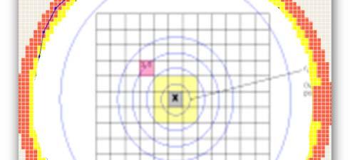
12 Production data example Prober needle realignment log data for 12 tested wafers 125 C) Probing time X correction Y correction Wafer to Wafer PTPA movements Z correction IEEE SW Test Workshop 12
13 Joint Cooperation & Motivation Temperature Influence on Probing Experimental data Results & Future Work IEEE SW Test Workshop 13
14 Overview DOE s In total 6 experiments including 45 wafers with 60 different settings were prepared DOE 1 Tool Comparison 10 wafers were prepared in order to compare inhouse solution to WaferWoRx DOE 2 Stepping pattern optimization 5 wafers were used DOE 3Realignment Optimization 17 wafers were analysed with a large temperature range and different realignment/soaktime settings IEEE SW Test Workshop 14
15 DOE 1 Tool Comparison Comparison of WaferwoRx with NXP solution 10 wafers were probed with intentionally generated, typical production probing errors. Probe card errors: pitch, role, yaw, etc. Prober errors: Scaling, orthogonality, overtravel, etc. Rudolph WaferwoRx and NXP inhouse inspection solution scanned all wafers All 10 errors identified ed by both machines and dteams Both machines capable to identify typical production errors, misalignments and maintenance issues IEEE SW Test Workshop 15
16 DOE 2 Stepping pattern optimization What is the best probing pattern for high temperatures? 5 Wafers were probed with different stepping patterns on wafer Probing paths created with MultiSiteOptimizer (MSO) by SPA Standard meander Radial and spiral starting in the middle Shortest and longest probing path Probed at 125 C without realignment Standard soak time 2min. after direct heating from 30 C to 125 C Probing configuration Accretech UF3000, Teradyne J750 Vertical Probecard, 104 beams Analysis done on WaferwoRx + MS Excel Additional analysis with Excel 2007 and Pivot Feature IEEE SW Test Workshop 16


17 DOE 2 MSO stepping pattern description Meander Radial Longest Way Spiral Shortest Way IEEE SW Test Workshop 17


18 DOE 2 WaferWoRx Y Scrub Position Meander Radial Longest Way What is best? Spiral + 5µm Shortest Way - 5µm IEEE SW Test Workshop 18


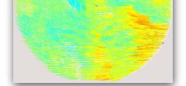
19 DOE 2 WaferWoRx Vector View Meander Radial Longest Way What is best? Spiral + 5µm Shortest Way - 5µm IEEE SW Test Workshop 19
20 DOE 2 Conclusion from WaferWoRx view Stepping Pattern recognized in plots Estimation possible on favorable pattern How do I get the probing time aligned with my analysis data? compare wafer results in one graph? get more flexibility to experiment with probemark data? Additional analysis with Excel 2007 and Pivot Feature IEEE SW Test Workshop 20


21 DOE 2 Total probe area Comparison of stepping patterns regarding probe area Meander Radial Longest Way 9µm 6µm 10µm 12µm 8µm 10µm Spiral Probemarks Shortest Way 12µm 6µ µm Total Probe area 80% Probe area 11µ µm one dot = av. of touchdown 8µm IEEE SW Test Workshop 21


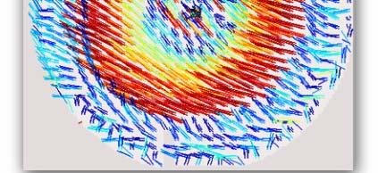
22 DOE 2 PTPA development Development of probe mark position resp. probing time Meander Radial Longest Way Spiral Time to PTPA Position Videos, very powerful! Shortest Way IEEE SW Test Workshop 22


 for")


23 DOE 2 X/Y Position change X/Y Postion [µm] over time (~1hour) for different stepping pattern Meander Radial Longest Way Useful chart type for Realignment definition Spiral Probing time Mean Y Scrub Position Shortest Way Mean X Scrub Position IEEE SW Test Workshop 23

![[µm] over time](/docs-images/81/83520911/images/24-1.jpg "(~1hour) for different")


24 DOE 2 Comparison Y Position Y Position [µm] over time (~1hour) for different stepping pattern Shortest Way Radial Spiral Longest way Meander Probing time IEEE SW Test Workshop 24

![[µm] over time](/docs-images/81/83520911/images/25-1.jpg "(~1hour) for different")


25 DOE 2 Comparison X Position X Postion [µm] over time (~1hour) for different stepping pattern Shortest Way Radial Spiral Longest way Meander Probing time IEEE SW Test Workshop 25
26 DOE 2 Results What is the best probing pattern for high temperatures? Significant probe to pad movement at 125 C All pattern need minimum one realignment Smallest movements with radial/spiral pattern Shortest and longest way unexpected large movements Longest way expensive very large index times WaferwoRx improvement proposals Time resolution 2D charts Datacomparison of several wafers in one graph Time resolution scatter plots Video scatter plots IEEE SW Test Workshop 26
27 DOE 3 Realignment Optimization What are the best realignment settings for extreme temperatures? 17 Wafers were probed with different temperatures/realignment/soaktime settings Cold, ambient, hot ( 60 C, 30 C, 125 C, 175 C, 200 C) Meander and Radial probing pattern for high temperatures Soaktime 2min and NXP std. realignment Probing configuration Accretech UF3000, Teradyne J750 Vertical lprobecard, 104 beams Analysis done on WaferwoRx + MS Excel AdditionalanalysiswithExcel analysis 2007andPivotFeature IEEE SW Test Workshop 27


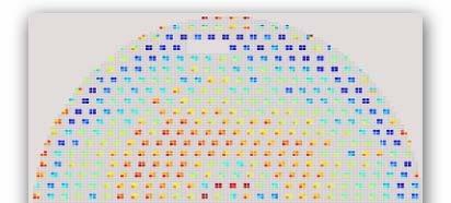


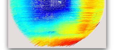
28 DOE 3 WaferWoRx Y Scrub Position -60 C 30 C 125 C How do I define realignment timings? + 5µm 175 C 200 C - 5µm IEEE SW Test Workshop 28


29 DOE 3 WaferWoRx Vector View -60 C 30 C 125 C How do I define realignment timings? + 5µm 175 C 200 C - 5µm IEEE SW Test Workshop 29
30 DOE 3 Conclusion from WaferWoRx view Expected temperature difference recognized in plots Realignment positions visible Estimation of optimized realignment settings difficult How do I get the probingtime aligned with my analysis data? include prober needle realigment data? get more flexibility to experiment with data? Additional analysis with Excel 2007 and Pivot Feature IEEE SW Test Workshop 30


![[µm] onedot](/docs-images/81/83520911/images/31-5.jpg "= av.")
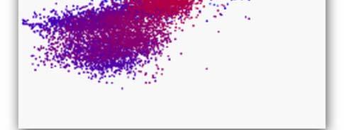
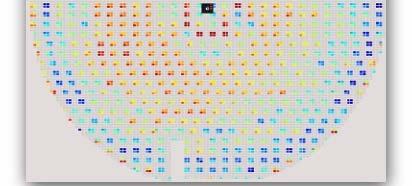
31 200 C Probemark Distribution Y Pad Dimension n [µm] Can we see realignments? X Pad Dimension [µm] onedot = av. oftouchdown IEEE SW Test Workshop 31
32 200 C Probemark Distribution Development of the probe position in time Y Pad Dimension n [µm] We re getting there X Pad Dimension [µm] IEEE SW Test Workshop 32


33 200 C Probemark Distribution Probemarks grouped in the realignment phases using Prober log data Yes we can! Y Pad Dimensio on [µm] Probemark position drift Until 1st realignment After 1st realignment After 2nd realignment After 3rd realignment X Pad Dimension [µm] onedot = av. oftouchdown IEEE SW Test Workshop 33


34 200 C Probemark Distribution Significance of realignment visible by comparing total probe area Realignment Probemark area is shrunk by factor µm 17µm Recalculation without Realignment 37µm 22µm onedot = av. oftouchdown IEEE SW Test Workshop 34

![X/Y Postion [µm]](/docs-images/81/83520911/images/35-2.jpg "over time")


35 DOE 3 X/Y Position change X/Y Postion [µm] over time (~1hour) for different temperatures -60 C 30 C 125 C Probing time 175 C 200 C Mean Y Scrub Position Mean X Scrub Position IEEE SW Test Workshop 35


 for")


36 DOE 3 Comparison Y Position Y Postion [µm] over time (~1hour) for different temperatures 200 C 175 C 125 C 30 C -60 C Probing time IEEE SW Test Workshop 36


 for")


37 DOE 3 Comparison X Position X Postion [µm] over time (~1hour) for different temperatures 200 C 175 C 125 C 30 C -60 C Probing time IEEE SW Test Workshop 37
38 DOE 3 Results What are the best realignment settings for extreme temperatures? All hot and cold probing temperatures show significant probe to pad movements Temperature distance to ambient is main driver 200 C with hbiggest probe to pad deviations i Realignments defined depending on probing temperature WaferWoRx improvement proposals Probe log data and map data input interface Realignment identification Raw data transformation and modification IEEE SW Test Workshop 38
39 Joint Cooperation & Motivation Temperature Influence on Probing Experimental data Results & Future Work IEEE SW Test Workshop 39
40 Results Successful process optimization Different stepping patterns evaluated Soak time and realignment settings optimized Up to 200 C tested and recipes defined Evaluation of WaferWoRx to in house tools done. Both are technically comparable. All standard errors were succesfully identified. Recommendations developed to improve WaferWoRx models and graphical user interface Temperature analysis needs timeresolution GUI Prober log data and map data input interface Raw data transformation and modification needed IEEE SW Test Workshop 40
41 Future Work Analyze and understand differences of different hardware combinations Improve test tcell hardware performance to reduce number of needed realignments Analysis results and method to be roled out in NXP IEEE SW Test Workshop 41
42 Acknowledgements Rudolph Technologies Darren James JP Kummer Rex Sandbach Sam Waggoner Accretech Maik Ehlen NXP Semiconductors Thomas Dabelstein Jens Däbritz Swen Mohr Providing NXP with oppurtunity to evaluate WaferWoRx and optimize performance. Working on preparation, data acquisition and analysis. IEEE SW Test Workshop 42


43 Questions? IEEE SW Test Workshop 43
HBM fine pitch micro pillar grid array probing evaluation
 HBM fine pitch micro pillar grid array probing evaluation Raffaele Vallauri, Technoprobe Daniele Perego, Technoprobe Marco Prea, Technoprobe Jaehong Kim, Samsung Electronics Jinyeong Yun, Samsung Electronics
Improving Yield for High Pin Count Wafer Probing Applications
 John R. Goulding Martin Elzingre Larry Hendler Technical Marketing Manager 200mm Product Manager Consultant Electroglas, Inc. Electroglas, Inc. Electroglas, Inc. South West Test Workshop June 11-14 th
Controlling BP Damage at 129C Probing
 ti 1010100111011 101001110111011 Controlling BP Damage at 129C Probing Daniel Fresquez, Eddie McClanahan and Al Wegleitner Texas Instruments, Dallas, TX June 11 th 2006 1 Outline Background the journey
October Suzhou - Shenzhen, China. Archive TestConX - Image: Breath10/iStock
 October 23-25 2018 Suzhou - Shenzhen, China Archive 2018 TestConX - Image: Breath10/iStock COPYRIGHT NOTICE The presentation(s)/poster(s) in this publication comprise the Proceedings of the 2018 TestConX
Impact of BGA Warpage on Quality. Mike Varnau
 Impact of BGA Warpage on Quality Mike Varnau 5-11-06 Contents What is a Ball in Cup Failure Case Study Background Problem Identification Solution Results Assembly Related Factors Causing Ball in Cup Component
Utilization of Egyptian Research Reactor and modes of collaboration
 Utilization of Egyptian Research Reactor and modes of collaboration Mohamed A. GAHEEN Director of ETRR-2, Egypt TM on Research Reactor Application for Materials Under High Neutron Fluence, Vienna, 17-21
Developments & Limitations in GSR Analysis
 Developments & Limitations in GSR Analysis ENFSI Working Group Meeting June 2006 Jenny Goulden Oxford Instruments NanoAnalysis Overview Introduction Developments in GSR Software Importance of EDS Hardware
A New Methodology for Assessing the Current Carrying Capability of Probes used at Sort
 Matthew C Zeman Intel Corporation A New Methodology for Assessing the Current Carrying Capability of Probes used at Sort June 6 to 9, 2010 San Diego, CA USA Overview Background ISMI Methodology (presented
1
 Process methodologies for temporary thin wafer handling solutions By Justin Furse, Technology Strategist, Brewer Science, Inc. Use of temporary bonding/debonding as part of thin wafer handling processes
Global 3D Machine Vision Market Report- Forecast till 2022
 Report Information More information from: https://www.marketresearchfuture.com/reports/1538 Global 3D Machine Vision Market Report- Forecast till 2022 Report / Search Code: MRFR/SEM/1009-HCRR Publish Date:
Nomenclature, Advantages, Applications. Logic States, Read Ops, Write Ops
 Critical Factors in Testing MRAM Devices W. Stevenson Cypress Semiconductor, Inc Inc. Southwest Test Workshop June G. Asmerom C. Taylor Electroglas AGENDA / OBJECTIVE MRAM Device? Nomenclature, Advantages,
WeatherWatcher ACP. Astronomers Control Panel (V4 or >) Ambient Virtual Weather Station (Pro or Internet editions) ASCOM platform v4.
 Ambient Virtual Weather Station (Pro or Internet editions) ASCOM platform v4.") WeatherWatcher ACP Software This is a minimum equipment list: Astronomers Control Panel (V4 or >) Ambient Virtual Weather Station (Pro or Internet editions) ASCOM platform v4.1 or higher Hardware Weather
WeatherWatcher ACP Software This is a minimum equipment list: Astronomers Control Panel (V4 or >) Ambient Virtual Weather Station (Pro or Internet editions) ASCOM platform v4.1 or higher Hardware Weather
A Novel Measurement Method for Measuring CCC and MAC at once
 A Novel Measurement Method for Measuring CCC and MAC at once Achim Weiland Gunther Böhm FEINMETALL GmbH Objectives New MEMS Product Large Scatter of Measurement Results Reproducable Characterization of
Reliable Test Results
 Intelligent testing Johannes J.Bührle - Agenda Reliable test results are a fundamental and highly topical aspect of materials testing. Using suitable examples we would like to show you how we view this
Microsystems Technology Laboratories i-stepperthursday, October 27, 2005 / site map / contact
 Microsystems Technology Laboratories i-stepperthursday, October 27, 2005 / site map / contact Fabrication BecomING an MTL Fab. User Internal MIT Users External Users Facilities Fab. staff MTL Orientation
Practical Considerations and Solutions for Temperature-Dependent S-Parameter Measurement for Accurate Parameter Extraction of
 Practical Considerations and Solutions for Temperature-Dependent S-Parameter Measurement for Accurate Parameter Extraction of Advanced RF Devices Gavin Fisher, Application Engineer Andrej Rumiantsev, Product
Determine the Inside Wall Temperature of DSTs using an Infrared Temperature Sensor
 SUMMARY DOCUMENT Determine the Inside Wall Temperature of DSTs using an Infrared Temperature Sensor Date submitted: April 14, 2017 Prepared by: Aparna Aravelli, Ph.D. Florida International University Collaborators:
A Novel Superior Low Force Probe Geometry Enabling Probing on Micro Bumps with Very Small Pitches
 A Novel Superior Low Force Probe Geometry Enabling Probing on Micro Bumps with Very Small Pitches (FM) Achim Weiland (FM) Gunther Böhm (FM) Franz Steger (TI) Overview History of the Buckling Beam Striped
A deeper investigation into the thermal drift of a linear axis
 A deeper investigation into the thermal drift of a linear axis O Beltrami STANIMUC Ente Federate UNI via A. Vespucci 7725 Torino, Italia Abstract This presentation shows the results of actual tests performed
Recent Advances in Optical Leak Testing (OLT)
") Recent Advances in Optical Leak Testing (OLT) Tom Trafford, Project Engineer IMAPS New England May 05, 2015 Theory of OLT (Optical Leak Test) Start Test End Test Hermetic Sealed Chamber Pressure Deforms
Recent Advances in Optical Leak Testing (OLT) Tom Trafford, Project Engineer IMAPS New England May 05, 2015 Theory of OLT (Optical Leak Test) Start Test End Test Hermetic Sealed Chamber Pressure Deforms
XBC300 Gen2. Fully-automated debonder and Cleaner
 XBC300 Gen2 Fully-automated debonder and Cleaner XBC300 Gen2 FULLY AUTOMATED DEBONDER AND CLEANER The SUSS XBC300 Gen2 debonder and cleaner platform is designed for process development as well as high
Machine Positioning Uncertainty with Laser Interferometer Feedback
 Machine Positioning Uncertainty with Laser Interferometer Feedback The purpose of this discussion is to explain the major contributors to machine positioning uncertainty in systems with laser interferometer
Determine the Inside Wall Temperature of DSTs using an Infrared Temperature Sensor
 SUMMARY DOCUMENT Determine the Inside Wall Temperature of DSTs using an Infrared Temperature Sensor Date submitted: July 29, 2016 Prepared by: Aparna Aravelli, Ph.D. Florida International University Collaborators:
Advanced Laser Surface Analyzer. Francis V. Krantz Ashland Inc Blazer Parkway Dublin, Ohio Abstract
 Advanced Laser Surface Analyzer Francis V. Krantz Ashland Inc. 5200 Blazer Parkway Dublin, Ohio 43017 Abstract The Advanced Laser Surface Analyzer (ALSA) is the result of continuing development of surface
Thermal aspects of 3D and 2.5D integration
 Thermal aspects of 3D and 2.5D integration Herman Oprins Sr. Researcher Thermal Management - imec Co-authors: Vladimir Cherman, Geert Van der Plas, Eric Beyne European 3D Summit 23-25 January 2017 Grenoble,
MEASUREMENT OF 3D FLOW FIELD IN A 90 BEND WITH ULTRASONIC DOPPLER VELOCITY PROFILER
 MEASUREMENT OF 3D FLOW FIELD IN A 90 BEND WITH ULTRASONIC DOPPLER VELOCITY PROFILER Daniel S. Hersberger 1 1 Research associate, Laboratory of Hydraulic Constructions (LCH), Swiss Federal Institute of
Magnetic Property Measurement System
 Magnetic Property Measurement System Product Description Quantum Design's MPMS 3 represents the culmination of more than 3 years of development and design in the world of SQUID Magnetometry. Providing
Application example. Measuring Force Sensors Rigid. Six series Nano, Mini, Gamma, Delta, Theta, Omega. Range of measurement, force ± 36 N..
 FT Six series Nano, Mini, Gamma, Delta, Theta, Omega Range of measurement, force ± 36 N.. ± 40000 N Range of measurement, moment ± 0.5 Nm.. ± 6000 Nm Application example Robot-supported chamfering of round
Towards Automatic Nanomanipulation at the Atomic Scale
 Towards Automatic Nanomanipulation at the Atomic Scale Bernd Schütz Department of Computer Science University of Hamburg, Germany Department of Computer Science Outline Introduction System Overview Workpackages
Acceleration, Velocity, Separate probe VIBRATION METER Model : VB-8202
 Acceleration, Velocity, Separate probe VIBRATION METER Model : VB-8202 Your purchase of this VIBRATION METER marks a step forward for you into the field of precision measurement. Although this METER is
novaa 800 D Atomic Absorption Spectrometer
 Technical Data Atomic Absorption Spectrometer Cpt : +27 (0) 21 905 0476 Jhb : +27 (0) 11 794 Dbn : +27 (0) 31 266 2454 1/7 General The is a compact atomic absorption spectrometer with deuterium background
BOWSER Balloon Observatory for Wavelength and Spectral Emission Readings
 COSGC Space Research Symposium 2009 BOWSER Balloon Observatory for Wavelength and Spectral Emission Readings BOWSER 1 Mission Premise 4.3 km above sea level 402.3km above sea level BOWSER 2 Information
GIS (GEOGRAPHIC INFORMATION SYSTEMS)
") GIS (GEOGRAPHIC INFORMATION SYSTEMS) 1 1. DEFINITION SYSTEM Any organised assembly of resources and procedures united and regulated by interaction or interdependence to complete a set of specific functions.
GIS (GEOGRAPHIC INFORMATION SYSTEMS) 1 1. DEFINITION SYSTEM Any organised assembly of resources and procedures united and regulated by interaction or interdependence to complete a set of specific functions.
TE 75R RESEARCH RUBBER FRICTION TEST MACHINE
 TE 75R RESEARCH RUBBER FRICTION TEST MACHINE Background: The Research Rubber Friction Test Machine offers the ability to investigate fully the frictional behaviour of rubbery materials both in dry and
Controlling Thermal Expansion
 Controlling Thermal Expansion Strategies for Maximizing the Repeatability of your Linear Stage By David Goosen, Mechanical Engineering Team INTRODUCTION Most of us are aware that all common engineering
In data sheets and application notes which still contain NXP or Philips Semiconductors references, use the references to Nexperia, as shown below.
 Important notice Dear Customer, On 7 February 2017 the former NXP Standard Product business became a new company with the tradename Nexperia. Nexperia is an industry leading supplier of Discrete, Logic
Table of Contents. DS163 LUXEON V Product Datasheet Lumileds Holding B.V. All rights reserved.
 Illumination LUXEON V Unmatched flux density with the lowest thermal resistance enabling never before possible form factors LUXEON V is a Chip Scale Package (CSP based high power emitter designed to deliver
In data sheets and application notes which still contain NXP or Philips Semiconductors references, use the references to Nexperia, as shown below.
 Important notice Dear Customer, On 7 February 207 the former NXP Standard Product business became a new company with the tradename Nexperia. Nexperia is an industry leading supplier of Discrete, Logic
OPERATION MANUAL. 3 in 1, IR, Type K/J/R/E/T, Pt 100 ohm THERMOMETER. Model : TM-2000
 3 in 1, IR, Type K/J/R/E/T, Pt 100 ohm THERMOMETER Model : TM-2000 Your purchase of this THERMOMETER marks a step forward for you into the field of precision measurement. Although this THERMOMETER is a
Thin Wafer Handling Challenges and Emerging Solutions
 1 Thin Wafer Handling Challenges and Emerging Solutions Dr. Shari Farrens, Mr. Pete Bisson, Mr. Sumant Sood and Mr. James Hermanowski SUSS MicroTec, 228 Suss Drive, Waterbury Center, VT 05655, USA 2 Thin
In data sheets and application notes which still contain NXP or Philips Semiconductors references, use the references to Nexperia, as shown below.
 Important notice Dear Customer, On 7 February 2017 the former NXP Standard Product business became a new company with the tradename Nexperia. Nexperia is an industry leading supplier of Discrete, Logic
High pulsed current wafer probing in high temperature conditions: comprehensive framework for vertical and cantilever probe design
 High pulsed current wafer probing in high temperature conditions: comprehensive framework for vertical and cantilever probe design D. Acconcia, R. Vettori Technoprobe R. Vallauri Technoprobe Outline Background
In data sheets and application notes which still contain NXP or Philips Semiconductors references, use the references to Nexperia, as shown below.
 Important notice Dear Customer, On 7 February 2017 the former NXP Standard Product business became a new company with the tradename Nexperia. Nexperia is an industry leading supplier of Discrete, Logic
ESPRIT Feature. Innovation with Integrity. Particle detection and chemical classification EDS
 ESPRIT Feature Particle detection and chemical classification Innovation with Integrity EDS Fast and Comprehensive Feature Analysis Based on the speed and accuracy of the QUANTAX EDS system with its powerful
HSG-IMIT Application AG
 B4.1 Acceleration Sensors IP-Blocks for MEMS Foundry Surface Micromachining Process R. Knechtel, S. Dempwolf S. Hering X-FAB Semiconductor Foundries AG Haarberstraße 67 99097 Erfurt / Germany T. Link J.
Ultrafast Nano Imprint Lithography
 Ultrafast Nano Imprint Lithography Imprint in less than 1 sec Logos Anti-counterfeiting nanostructures Miniaturized QRs Customized designs 2 Pulsed-NIL technology enables printing times in less than 100
Update in Material and Process Technologies for 2.5/3D IC Dr. Rainer Knippelmeyer CTO and VP R&D, SÜSS MicroTec AG
 Update in Material and Process Technologies for 2.5/3D IC Dr. Rainer Knippelmeyer CTO and VP R&D, SÜSS MicroTec AG TEMPORARY BONDING / DEBONDING AS THIN WAFER HANDLING SOLUTION FOR 3DIC & INTERPOSERS Device
Lattice Cell/Girder Assembly
 SPEAR3 Magnets Jack Tanabe, Nanyang Li, Ann Trautwein, Domenico Dell Orco, Dave Ernst, Zach Wolf (SLAC Magnet Measurements), Catherine L Coq (SLAC Alignment), Jeff Corbett, Bob Hettel (SPEAR3 Physics)
Advancements in mm-wave On-Wafer Measurements: A Commercial Multi-Line TRL Calibration Author: Leonard Hayden Presenter: Gavin Fisher
 Advancements in mm-wave On-Wafer Measurements: A Commercial Multi-Line TRL Calibration Author: Leonard Hayden Presenter: Gavin Fisher The title of this section is A Commercial Multi-Line TRL Calibration
Memory Thermal Management 101
 Memory Thermal Management 101 Overview With the continuing industry trends towards smaller, faster, and higher power memories, thermal management is becoming increasingly important. Not only are device
THERMAL DESIGN OF POWER SEMICONDUCTOR MODULES FOR MOBILE COMMNICATION SYSYTEMS. Yasuo Osone*
 Nice, Côte d Azur, France, 27-29 September 26 THERMAL DESIGN OF POWER SEMICONDUCTOR MODULES FOR MOBILE COMMNICATION SYSYTEMS Yasuo Osone* *Mechanical Engineering Research Laboratory, Hitachi, Ltd., 832-2
1 INTRODUCTION 2 SAMPLE PREPARATIONS
 Chikage NORITAKE This study seeks to analyze the reliability of three-dimensional (3D) chip stacked packages under cyclic thermal loading. The critical areas of 3D chip stacked packages are defined using
150 V, 2 A NPN high-voltage low V CEsat (BISS) transistor
 transistor") Rev. 0 November 2009 Product data sheet. Product profile. General description NPN high-voltage low V CEsat Breakthrough In Small Signal (BISS) transistor in a medium power SOT223 (SC-73) Surface-Mounted
Rev. 0 November 2009 Product data sheet. Product profile. General description NPN high-voltage low V CEsat Breakthrough In Small Signal (BISS) transistor in a medium power SOT223 (SC-73) Surface-Mounted
Acceleration/Velocity/Displacement VIBRATION METER
 Acceleration/Velocity/Displacement VIBRATION METER Model : VB-8220 Your purchase of this VIBRATION METER marks a step forward for you into the field of precision measurement. Although this METER is a complex
Coupling Capacitance in Face-to-Face (F2F) Bonded 3D ICs: Trends and Implications
 Bonded 3D ICs: Trends and Implications") Coupling Capacitance in Face-to-Face (F2F) Bonded 3D ICs: Trends and Implications Taigon Song *1, Arthur Nieuwoudt *2, Yun Seop Yu *3 and Sung Kyu Lim *1 *1 School of Electrical and Computer Engineering,
Coupling Capacitance in Face-to-Face (F2F) Bonded 3D ICs: Trends and Implications Taigon Song *1, Arthur Nieuwoudt *2, Yun Seop Yu *3 and Sung Kyu Lim *1 *1 School of Electrical and Computer Engineering,
In data sheets and application notes which still contain NXP or Philips Semiconductors references, use the references to Nexperia, as shown below.
 Important notice Dear Customer, On 7 February 207 the former NXP Standard Product business became a new company with the tradename Nexperia. Nexperia is an industry leading supplier of Discrete, Logic
PYCKO SCIENTIFIC LIMITED
 PYCKO SCIENTIFIC LIMITED 31 London Road, Grantham, NG31 6EX Telephone 01476 401992 bill@pycko.co.uk www.pycko.co.uk Your Alternative To The Obvious RayMon10 TM Detect, measure, identify and analyse radionuclides
Appendix G. Thermal analysis of a piezo-actuated pointing mechanism. Paul Lardet (Sodern, France)
") 95 Appendix G Thermal analysis of a piezo-actuated pointing mechanism Paul Lardet (Sodern, France) 96 Thermal analysis of a piezo-actuated pointing mechanism Abstract For the pointing of the Earthcare
95 Appendix G Thermal analysis of a piezo-actuated pointing mechanism Paul Lardet (Sodern, France) 96 Thermal analysis of a piezo-actuated pointing mechanism Abstract For the pointing of the Earthcare
Overview. 1. Terms and Definitions. 2. Model Identification. 3. Path Coefficients
 2. The Basics Overview 1. Terms and Definitions 2. Model Identification 3. Path Coefficients 2.1 Terms and Definitions 2.1 Terms & Definitions. Structural equation model = observed, latent, composite Direct
CALIBRATION. Calibration. General Principles & Theory, Equipment Considerations. Copyright Caltech 2014
 Calibration General Principles & Theory, Equipment Considerations Metrological Principles Accurate but not Precise Calibration A A+ Correction = Precise but not Accurate Correction B Ref Std (Radio Link
Translational Biomarker Core
 Translational Biomarker Core Instrumentation Thermo Scientific TSQ Quantum Triple Quadrupole Mass Spectrometers. There are two TSQ Quantum Ultra AM instruments available in the TBC. The TSQ Quantum Ultra
i.mx 6 Temperature Sensor Module
 NXP Semiconductors Document Number: AN5215 Application Note Rev. 1, 03/2017 i.mx 6 Temperature Sensor Module 1. Introduction All the i.mx6 series application processors use the same temperature sensor
LUXEON UV U1. Highest power density, superior efficiency, powered by leading Chip Scale Package (CSP) technology ILLUMINATION
 technology ILLUMINATION") ILLUMINATION LUXEON UV U1 Highest power density, superior efficiency, powered by leading Chip Scale Package (CSP) technology At 1/5 th the size of other ultraviolet and violet LEDs, LUXEON UV U1 LEDs,
ILLUMINATION LUXEON UV U1 Highest power density, superior efficiency, powered by leading Chip Scale Package (CSP) technology At 1/5 th the size of other ultraviolet and violet LEDs, LUXEON UV U1 LEDs,
Introduction to Fourier Transform Infrared Spectroscopy
 Introduction to Fourier Transform Infrared Spectroscopy Introduction What is FTIR? FTIR stands for Fourier transform infrared, the preferred method of infrared spectroscopy. In infrared spectroscopy, IR
BRIGHT-STRATO SERIES
 Coordinate Measuring Machines BRIGHT-STRATO SERIES CNC Coordinate Measuring Machine Bulletin No. 1855 Moving-bridge type CMM with excellent measuring accuracy. Its measuring envelope is suitable for medium-to-large
In data sheets and application notes which still contain NXP or Philips Semiconductors references, use the references to Nexperia, as shown below.
 Important notice Dear Customer, On 7 February 2017 the former NXP Standard Product business became a new company with the tradename Nexperia. Nexperia is an industry leading supplier of Discrete, Logic
Dielectric Analysis of Solid Insulations
 using Dielectric Test Fixture 16451B from Keysight By Britta Pfeiffer 2018 by OMICRON Lab V2.0 Visit www.omicron-lab.com for more information. Contact support@omicron-lab.com for technical support. Page
CNES R&D and available software for Space Images based risk and disaster management
 CNES R&D and available software for Space Images based risk and disaster management 1/21 Contributors: CNES (Centre National d Etudes Spatiales), Toulouse, France Hélène Vadon Jordi Inglada 2/21 Content
MODEL NAME : LLDMWW0-15K*0*A
 Eagle Eye (Outdoor LED Module) Application Note MODEL NAME : LLDMWW0-15K*0*A RoHS Compliant HALOGEN FREE (30)-4022 1 / 16 CONTENTS 1. Product Description 3/16 2. Specifications 2.1. Chromaticity Bins for
THE UTP SUITE YOUR ALL-IN-ONE SOLUTION FOR BUILDING MODERN TEST SYSTEM SOFTWARE
 THE UTP SUITE YOUR ALL-IN-ONE SOLUTION FOR BUILDING MODERN TEST SYSTEM SOFTWARE UTP Suite THE UTP SUITE DEVELOPING A STANDARD Increasing customer requirements, shorter product cycles and higher time to
LHC ORBIT SYSTEM, PERFORMANCE AND STABILITY
 LHC ORBIT SYSTEM, PERFORMANCE AND STABILITY Kajetan Fuchsberger Abstract During the LHC run period in 2009 the Orbit system proved to be very reliable. In the following the analysis results of the first
Technology Improvement and Fault TCP Etch Chamber and a Dual Frequency Oxide Etch Chamber
 Technology Improvement and Fault Detection @ TCP Etch Chamber and a Dual Frequency Oxide Etch Chamber Russell Benson, Micron Daniel Steckert, Micron Lutz Eichhorn, Plasmetrex Michael Klick, Plasmetrex
Nuclear Associates
 Nuclear Associates 37-001 TEL-ALIGN Teletherapy Alignment Gauge Users Manual March 2005 Manual No. 37-001-1 Rev. 2 2004, 2005 Fluke Corporation, All rights reserved. Printed in U.S.A. All product names
The Increasing Importance of the Thermal Management for Modern Electronic Packages B. Psota 1, I. Szendiuch 1
 Ročník 2012 Číslo VI The Increasing Importance of the Thermal Management for Modern Electronic Packages B. Psota 1, I. Szendiuch 1 1 Department of Microelectronics, Faculty of Electrical Engineering and
Mnova Software for Analyzing Reaction Monitoring NMR Spectra
 Mnova Software for Analyzing Reaction Monitoring NMR Spectra Version 10 Chen Peng, PhD, VP of Business Development, US & China Mestrelab Research SL San Diego, CA, USA chen.peng@mestrelab.com 858.736.4563
Nanoscale IR spectroscopy of organic contaminants
 The nanoscale spectroscopy company The world leader in nanoscale IR spectroscopy Nanoscale IR spectroscopy of organic contaminants Application note nanoir uniquely and unambiguously identifies organic
Hybrid Wafer Level Bonding for 3D IC
 Hybrid Wafer Level Bonding for 3D IC An Equipment Perspective Markus Wimplinger, Corporate Technology Development & IP Director History & Roadmap - BSI CIS Devices???? 2013 2 nd Generation 3D BSI CIS with
Department Mission: Mandated Services: Department Overview: Successes and Challenges:
 Department: Information Technology FY 2019 Proposed Budget Department Mission: Klamath County Information Technology delivers business services that empower, support and serve all county departments in
Overview of Modeling and Simulation TCAD - FLOOPS / FLOODS
 Overview of Modeling and Simulation TCAD - FLOOPS / FLOODS Modeling Overview Strain Effects Thermal Modeling TCAD Modeling Outline FLOOPS / FLOODS Introduction Progress on GaN Devices Prospects for Reliability
print close Related Picking PCB Materials for Microwave Amps Matching Circuit Materials to a Design Mission Perusing Materials For High-Frequency PCBs
 print close Microwaves and RF Jack Browne Mon, 2015-08-03 12:51 Sorting through different RF/microwave circuit materials educed comparisons of performance improvements and cost hikes, although some materials
Radio Observation of Milky Way at MHz. Amateur Radio Astronomy Observation of the Milky Way at MHz from the Northern Hemisphere
 Amateur Radio Astronomy Observation of the Milky Way at 1453.5MHz from the Northern Hemisphere Dr David Morgan February 2011 Introduction The measurements reported here were made in March and April 2007
NPN/PNP low V CEsat Breakthrough in Small Signal (BISS) transistor pair in a SOT457 (SC-74) Surface Mounted Device (SMD) plastic package.
 transistor pair in a SOT457 (SC-74) Surface Mounted Device (SMD) plastic package.") Rev. 03 11 December 2009 Product data sheet 1. Product profile 1.1 General description NPN/PNP low V CEsat Breakthrough in Small Signal (BISS) transistor pair in a SOT457 (SC-74) Surface Mounted Device
Rev. 03 11 December 2009 Product data sheet 1. Product profile 1.1 General description NPN/PNP low V CEsat Breakthrough in Small Signal (BISS) transistor pair in a SOT457 (SC-74) Surface Mounted Device
FRAUNHOFER INSTITUTE FOR SURFACE ENGINEERING AND THIN FILMS IST ATMOSPHERIC PRESSURE PLASMA PROCESSES
 FRAUNHOFER INSTITUTE FOR SURFACE ENGINEERING AND THIN FILMS IST ATMOSPHERIC PRESSURE PLASMA PROCESSES 1 2 ATMOSPHERIC PRESSURE PLASMA PROCESSES AT THE FRAUNHOFER IST Today, atmospheric pressure plasma
MPC-D403 MPC-D404. Ultra-small Peltier Coolers. High impedance Low control current High power efficiency
 MPC-D MPC-D Ultra-small Peltier Coolers High impedance Low control current High power efficiency MPC-D / D. Introduction. General description The MPC- / D micro chip-sized thermoelectric coolers (TEC)
Best selling products overview of company AURA a.s.
 Best selling products overview of company AURA a.s. The most frequent areas of application of AURA a. s. products Petrol industry Mines and mining industry Metallurgy and heavy industry Deliveries for
ISSP User Guide CY3207ISSP. Revision C
 CY3207ISSP ISSP User Guide Revision C Cypress Semiconductor 198 Champion Court San Jose, CA 95134-1709 Phone (USA): 800.858.1810 Phone (Intnl): 408.943.2600 http://www.cypress.com Copyrights Copyrights
ionos The most advanced stable isotope software ever created
 ionos The most advanced stable isotope software ever created ionos Fast and robust data processing of the most complex samples ionos is the most advanced software ever created for the stable isotope community.
Mid High Latitude Cirrus Precipitation Processes. Jon Sauer, Dan Crocker, Yanice Benitez
 Mid High Latitude Cirrus Precipitation Processes Jon Sauer, Dan Crocker, Yanice Benitez Department of Chemistry and Biochemistry, University of California, San Diego, CA 92093, USA *To whom correspondence
High Accuracy High Speed in Your Process
 DX-Series Handheld Precision IR Thermometers EXERGEN C O R P O R A T I O N The Only Certified Accurate NIST Traceable Infrared Temperature Instruments in the World* High Accuracy High Speed in Your Process
CesrTA Status Report Mark Palmer for the CesrTA Collaboration March 4, 2009 ESR
 CesrTA Status Report Mark Palmer for the CesrTA Collaboration March 4, 2009 ESR Outline Recent Updates January run/february Down Overview Optics & LET xbsm Electron Cloud Studies Tune Data-Simulation Comparisons
Humidity Calibration Solutions
 Instruments Humidity Solutions www.michell.com Instruments Humidity Solutions The Importance of Regular The reliable operation of a hygrometer and indeed any measuring instrument, can only be verified
Sensors & Transducers Published by IFSA Publishing, S. L., 2016
 Sensors & Transducers Published by IFSA Publishing, S. L., 2016 http://www.sensorsportal.com Ice Detection of Pure and Saline Ice Using Infrared Signature 1 Taimur Rashid, Hassan A. Khawaja and K. Edvardsen
Coromant Capto Short Adapter
 Coromant Capto Short Adapter The quick change system for reduced setup and production time. Faster return on investment. Short Adapter Short Adapter More available cutting tool length Short toolholder
New concept of a 3D-probing system for micro-components
 Research Collection Journal Article New concept of a 3D-probing system for micro-components Author(s): Liebrich, Thomas; Kanpp, W. Publication Date: 2010 Permanent Link: https://doi.org/10.3929/ethz-a-006071031
Augmented Reality Market Research Report- Global Forecast till 2023
 Report Information More information from: https://www.marketresearchfuture.com/reports/1143 Augmented Reality Market Research Report- Global Forecast till 2023 Report / Search Code: MRFR/ICT/0637-HCRR
Picometre metrology. The Gaia mission will create an ultra-precise three-dimensional map of about one billion stars
 Picometre metrology in space The Gaia mission will create an ultra-precise three-dimensional map of about one billion stars in our Galaxy. Part of ESA s Cosmic Vision program, the Gaia spacecraft is being
Data Sheet. ADJD-xMxx. High Power Light Strip, Ring & Round. Description. Features. Applications. Specifications
 ADJD-xMxx High Power Light Strip, Ring & Round Data Sheet Description Avago s Light Strip, Ring & Round Power LEDs range of products offers a series of LEDs which provides better lifetime robustness and
IMPLEMENTATION AND EXPERIENCE WITH LUMINOSITY LEVELLING WITH OFFSET BEAM
 IMPLEMENTATION AND EXPERIENCE WITH LUMINOSITY LEVELLING WITH OFFSET BEAM F. Follin, D. Jacquet, CERN, Geneva, Switzerland Abstract The practice of luminosity levelling with an offset beam has been used
Open Access Repository eprint
 Open Access Repository eprint Terms and Conditions: Users may access, download, store, search and print a hard copy of the article. Copying must be limited to making a single printed copy or electronic
Proceedings. BiTS Shanghai October 21, Archive - Session BiTS Workshop Image: Zhu Difeng/Dollar Photo Club
 Proceedings Archive - Session 1 2015 BiTS Workshop Image: Zhu Difeng/Dollar Photo Club Proceedings With Thanks to Our Sponsors! Premier Honored Distinguished Publication Sponsor 2 Proceedings Presentation