Zero Group Velocity Modes of Insulator Metal Insulator and Insulator Insulator Metal Waveguides
|
|
|
- Reginald Collins
- 5 years ago
- Views:
Transcription
 Dolgoprudny, Russia e mail: feddu@mail.")
1 Zero Group Velocity Modes of Insulator Metal Insulator and Insulator Insulator Metal Waveguides Dmitry Fedyanin, Aleksey Arsenin, Vladimir Leiman and Anantoly Gladun Department of General Physics, Moscow Institute of Physics and Technology (State University) Dolgoprudny, Russia e mail: feddu@mail.ru Acknowledgement: Vladimir Tarakanov, the athor of PIC code "KARAT"
2 OUTLINE Lossless case: Dispersion relations and dispersion curves of SPPs in IMI and IIM waveguide structures Existence conditions of waves with zero group velocity Lossy case: Effect of losses on dispersion curves Numerical calculations of energy velocity An analysis of points of zero energy velocity Excitation of zero group velocity modes Results of numerical simulation Applications
3 History Backward waves and waves with zero group velocity are typically associated with periodic structures. Nevertheless a periodicity is not the only way to obtain such waves - particularly investigations of slow wave propagation in plasma-dielectric structures showed that plasma waveguides with a specially designed circular cross section allow the existence of backward waves, so are some kinds of planar plasma waveguides: Trivelpiece A W, Gould R W 1959 Space charge waves in cylindrical plasma columns J. Appl. Phys. 30, Paik S F 1962 A backward wave in plasma waveguide Proc. IRE Allis W P, Buchsbaum S J, Bers A 1963 Waves in Anisotropic Plasma (Cambridge, MA: M.I.T. Press) Oliner A A, Tamir T 1962 Backward waves on isotropic plasma slabs J. Appl. Phys Schumann W O 1960 Z. angew Phys. 12, 4, 145
4 Lossless case Metal is described by Drude Zener model:
5 Dispersion Relation, where and a is a half thickness of the film For IMI waveguide structures with ε2=ε3 dispersion relation can be easily simplified and rearranged as two branches: κ 2 ε1 th κ 1 a = κ1 ε2 anti symmetric mode κ1 ε2 th κ 1 a = κ2 ε1 symmetric mode
 IMI AS S")


6 Dispersion Curves (Lossless Case) IMI AS S AS anti symmetric mode, S symmetric mode AS S IIM ε2>ε3 The decay constant κ2 may be complex while κ1 and κ3 are real.
7 Existence Conditions of Waves with Zero Group Velocity Equation for Poynting vector in a complex form SPP's group velocity is negative if and only if net energy flux is opposite to the phase velocity direction that could be written as [ Allis W P, Buchsbaum S J, Bers A 1963 Waves in anisotropic plasma ] and the group velocity is zero if It will be recall that the only non radiative modes interest us, thus the projection of net power flow on z axis is equal to zero., where k = ω /c and


 x IMI?")

8 Existence Conditions of Waves with Zero Group Velocity Re(Sx) x IMI? IIM Single metal insulator interface


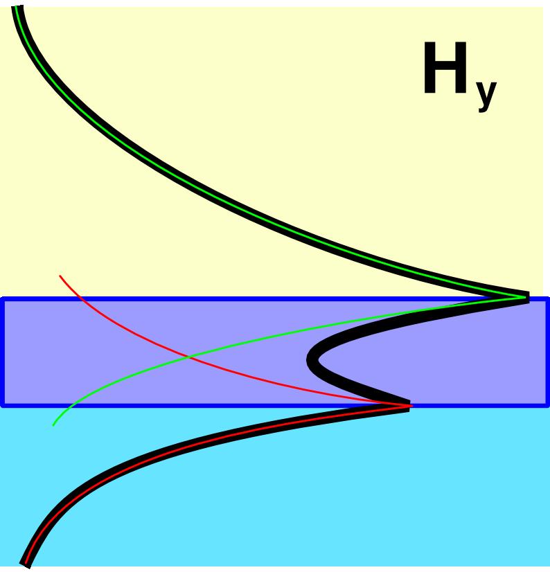

9 Existence Conditions of Waves with Zero Group Velocity IMI IIM small kx large kx small kx large kx
 to the power flow in dielectric media.")
10 Existence Conditions of Waves with Zero Group Velocity (IMI structures) In order to satisfy the existence condition of waves with zero group velocity the power flow inside the metal must be equal (in absolute value) to the power flow in dielectric media. Solving Maxwell equations we obtain that this requirement is equivalent to the following equality This lengthy expression can be significantly simplified in case of anti symmetric mode and ε2=ε3: [ Allis W P, Buchsbaum S J, Bers A 1963 Waves in anisotropic plasma, chapter 7 ]
.")
11 Existence Conditions of Waves with Zero Group Velocity (IMI structures) silver Dispersion curves of SPP in the insulator silver insulator structures for various permittivities. Non radiative modes are presented. The value of ε2 is fixed and is equal to 2.5, film thickness d=15 nm. Permittivity ε3 takes values from 1 till 12 (1; 2; 2.5; 3; 4; 5; 7; 12). The upper curve corresponds to ε3=1. According to [Palik E D 1998 Handbook of Optical Constants of Solids I (San Diego, CA: Academic Press) ] and Drude Zener model in a wavelength range nm [ Johnson P B, Christy R W 1972 Phys Rev B 6, 4370 ]
12 Existence Conditions of Waves with Zero Group Velocity (IMI structures) silver Zero group velocity points of the dispersion curves of SPPs as parametric functions of permittivity ε3. Permittivity ε3 takes values from 1 till 20. The value of ε2 is fixed (three materials are considered ZrO 2, SiO2, Al2O3 with permittivities 5.5, 2.2 and 2.84 correspondibly), film thickness d=15 nm.
13 Existence Conditions of Waves with Zero Group Velocity (IMI structures) silver Zero group velocity points of the dispersion curves of SPPs as parametric functions of permittivity ε3. Permittivity ε3 takes values from 1 till 20. The value of ε2 is fixed (three materials are considered ZrO2, SiO2, Al2O3 with permittivities 5.5, 2.2 and 2.84 correspondibly), film thickness d=15 nm.
14 Existence Conditions of Waves with Zero Group Velocity (IMI structures) Zero group velocity points of the dispersion curves of SPPs as parametric functions of permittivity ε3. Permittivity ε3 takes values from 1 till 20. The value of ε2 is fixed (three materials are considered ZrO2, SiO2, Al2O3 with permittivities 5.5, 2.2 and 2.84 correspondibly), film thickness d=15 nm.
15 Existence Conditions of Waves with Zero Group Velocity (IMI structures) Zero group velocity points of the dispersion curves of SPPs as parametric functions of film thickness d which takes values from 3 nm till 50 nm. The values of ε2 and ε3 are fixed.
16 Existence Conditions of Waves with Zero Group Velocity (IMI structures) Zero group velocity points of the dispersion curves of SPPs as parametric functions of film thickness d which takes values from 3 nm till 50 nm. The values of ε2 and ε3 are fixed.


17 Existence Conditions of Waves with Zero Group Velocity (IMI structures) Resonance circular frequency as function of permittivites of surrounding insulator media for fixed value of film thickness d. d=10 nm d=15 nm
18 Existence Conditions of Waves with Zero Group Velocity (IIM structures) vacuum silver Dispersion curves of SPP in the vacuum insulator silver structures for various permittivities ε2. Film thickness d=8 nm.
19 Existence Conditions of Waves with Zero Group Velocity (IIM structures) vacuum silver Zero group velocity points of the dispersion curves of SPPs as parametric functions of permittivity ε2. Permittivity ε2 takes values from 1 till 15. The value of ε3 is fixed (vacuum). Film thickness is fixed too, and three different values are considered.
20 Existence Conditions of Waves with Zero Group Velocity (IIM structures) Zero group velocity points of the dispersion curves of SPPs as parametric functions of permittivity ε2. Permittivity ε2 takes values from 1 till 15. The value of ε3 is fixed (vacuum). Film thickness is fixed too, and three different values are considered.
21 Existence Conditions of Waves with Zero Group Velocity (IIM structures) vacuum silver Dispersion curves of SPP in the vacuum insulator silver structures for various film thicknesses. Permittivity ε2=5.5 (ZrO2)
22 Existence Conditions of Waves with Zero Group Velocity (IIM structures) vacuum λ=350 nm silver Zero group velocity points of the dispersion curves of SPPs as parametric functions of film thickness d which takes values from 2nm till 20nm. The value of ε3 is fixed (vacuum). Four different materials as medium 2 are considered. dcoff is a cutoff thickness, i.e. the maximum thickness that allow the existence of zero group velocity mode. λ=450 nm
23 Existence Conditions of Waves with Zero Group Velocity (IIM structures) Zero group velocity points of the dispersion curves of SPPs as parametric functions of film thickness d which takes values from 2nm till 20nm. The value of ε3 is fixed (vacuum). Four different materials as medium 2 are considered.
24 Lossy case Metal is described by Drude Zener model:
25 Drude Zener dielectric function with dumping factor Silver: Γ 7 10 s 13 1
26 Effect of Losses on Dispersion Curves silver IMI Al2O3 Dispersion curves of SPP in the Al2O3 silver insulator structures for various permittivities ε2. Film thickness d=10 nm. Dashed lines show dispersion curves in a lossless system. Only the region, where Im(kx) < Re(kx), is considered.
27 Effect of Losses on Dispersion Curves IMI
28 Effect of Losses on Dispersion Curves IMI A B C D Re( ) Film thickness d=10 nm. Dashed lines show dependecies for lossless systems. Only the region, where Re(kx) >(ω/c) max(ε2,ε3), is considered. Points A, B, C, D correspond to cross points of dispersion curves with light lines.
29 Effect of Losses on Dispersion Curves vacuum IIM silver Dispersion curves of SPP in the vacuum insulator silver structures for various permittivities ε2. Film thickness d=8 nm. Dashed lines show dispersion curves in a lossless system. Only the region, where Im(kx) < Re(kx), Re( ) is considered.
30 Effect of Losses on Dispersion Curves B A B A C C Re ( ) Dispersion curves of SPP in the vacuum insulator silver. Film thickness d=8 nm. Negative values of Im(kx) correspond to backward waves. IIM Im(kx) < Re(kx)
31 Modified Drude Zener model Γ=Γ0+β ω 2 Γ0= s 18 β= s 13 [ Chen L, Lynch D W 1987 Phys Rev B 36, 1425 ] (red curve) 1
32 Effect of Losses on Dispersion Curves (cm 1) Dispersion curves of SPP in the vacuum insulator silver structures for various permittivities ε2. Modified Drude Zener model is used. Film thickness d=8 nm. Im(kx) < Re(kx)
33 Effect of Losses on Dispersion Curves vacuum Al2O3 silver Comparison of dispersion curves with different dumping factors Γ. Silver dielectric function obeys Drude Zener model. Silver is covered by ultra thin insulator film of Al2O3. Film thickness d=8 nm. Im(kx) < Re(kx) IIM
34 Effect of Losses on Dispersion Curves IIM vacuum Al2O3 silver Dispersion curves of SPP in the vacuum insulator silver structures for various dumping factors Γ. Film thickness d=8 nm.
35 Excitation of Zero Group Velocity Modes


36 Excitation of Zero Group Velocity Modes Three-layer Kretschmann geometry IMI εpr > ε2, ε3 Three-layer Kretschmann geometry or Otto configuration εpr > ε2> ε3 IIM Simple Kretschmann geometry εpr > ε2> ε3


37 Excitation of Zero Group Velocity Modes
38 Results of Numerical Simulation and Applications

39 Stored Light in Nano Scale Plasmonic Cavity s=50 nm Γ= s 1 d=10 nm L=180 nm and Γ= s 1 IMI εpr=7.4 ϴ=45⁰ ω= s 1
40 Stored Light in Nano Scale Plasmonic Cavity IMI
 point A point B")
41 Stored Light in Nano Scale Plasmonic Cavity Γ=7 10 s 12 1 E=E0 sin(ω t) point A point B IMI
 IMI point A point B V=V0 sin(ω t)")
42 Stored Light in Nano Scale Plasmonic Cavity Γ=7 10 s 12 1 E=E0 sin(ω t) IMI point A point B V=V0 sin(ω t)


43 Stored Light in Nano Scale Plasmonic Cavity Γ=7 10 s 12 1 IMI

44 Stored Light in Nano Scale Plasmonic Cavity IMI Γ= s 1

45 Future
46 Thank you for your attention! Dmitry Fedyanin, Aleksey Arsenin, Vladimir Leiman and Anantoly Gladun Moscow Institute of Physics and Technology (State University), Russia e mail: feddu@mail.ru
Surface Plasmon-polaritons on thin metal films - IMI (insulator-metal-insulator) structure -
 structure -") Surface Plasmon-polaritons on thin metal films - IMI (insulator-metal-insulator) structure - Dielectric 3 Metal 2 Dielectric 1 References Surface plasmons in thin films, E.N. Economou, Phy. Rev. Vol.182,
Surface Plasmon-polaritons on thin metal films - IMI (insulator-metal-insulator) structure - Dielectric 3 Metal 2 Dielectric 1 References Surface plasmons in thin films, E.N. Economou, Phy. Rev. Vol.182,
II Theory Of Surface Plasmon Resonance (SPR)
") II Theory Of Surface Plasmon Resonance (SPR) II.1 Maxwell equations and dielectric constant of metals Surface Plasmons Polaritons (SPP) exist at the interface of a dielectric and a metal whose electrons
II Theory Of Surface Plasmon Resonance (SPR) II.1 Maxwell equations and dielectric constant of metals Surface Plasmons Polaritons (SPP) exist at the interface of a dielectric and a metal whose electrons
Surface Plasmon-polaritons on thin metal films
 Surface Plasmon-polaritons on thin metal films Dielectric ε 3 Metal ε 2 Dielectric ε 1 References Surface plasmons in thin films, E.N. Economou, Phy. Rev. Vol.182, 539-554 (1969) Surface-polariton-like
sgsp agsp W=20nm W=50nm Re(n eff (e) } Re{E z Im{E x Supplementary Figure 1: Gap surface plasmon modes in MIM waveguides.
 } Re{E z Im{E x Supplementary Figure 1: Gap surface plasmon modes in MIM waveguides.") (a) 2.4 (b) (c) W Au y Electric field (a.u) x SiO 2 (d) y Au sgsp x Energy (ev) 2. 1.6 agsp W=5nm W=5nm 1.2 1 2 3 4.1.1 1 1 Re(n eff ) -1-5 5 1 x (nm) W = 2nm E = 2eV Im{E x } Re{E z } sgsp Electric field
(a) 2.4 (b) (c) W Au y Electric field (a.u) x SiO 2 (d) y Au sgsp x Energy (ev) 2. 1.6 agsp W=5nm W=5nm 1.2 1 2 3 4.1.1 1 1 Re(n eff ) -1-5 5 1 x (nm) W = 2nm E = 2eV Im{E x } Re{E z } sgsp Electric field
LONG-RANGE SURFACE POLARITONS
 LONG-RANGE SURFACE POLARITONS IN THIN LAYERS OF ABSORBING MATERIALS Yichen Zhang Cover image: a surface wave induced by a water drop. This wave is propagating at the interface between water and air. ISBN:
Surface plasmon waveguides
 Surface plasmon waveguides Introduction Size Mismatch between Scaled CMOS Electronics and Planar Photonics Photonic integrated system with subwavelength scale components CMOS transistor: Medium-sized molecule
The observation of super-long range surface plasmon polaritons modes and its application as sensory devices
 The observation of super-long range surface plasmon polaritons modes and its application as sensory devices X. -L. Zhang, 1,2 J. -F. Song, 1,2,3,4 G. Q. Lo, 2 and D. -L. Kwong 2 1 State Key Laboratory
Enhanced Surface Plasmon Polariton Propagation Induced by Active Dielectrics
 E x c e Enhanced Surface Plasmon Polariton Propagation Induced by Active Dielectrics C. Athanasopoulos 1,, M. Mattheakis *1, 1,, and G. P. Tsironis 1 Crete Center for Quantum Complexity and Nanotechnology,
Introduction. Chapter Optics at the Nanoscale
 Chapter 1 Introduction 1.1 Optics at the Nanoscale The interaction of light with matter is one of the most significant processes on the planet, forming the basis of some of the most famous scientific discoveries
The physics of the perfect lens
 The physics of the perfect lens J.B. Pendry and S.A. Ramakrishna, The Blackett Laboratory, Imperial College, London MURI-Teleconference #2 Pendry s proposal for a perfect lens Consider Veselago s slab
FDTD Simulations of Surface Plasmons Using the Effective Permittivity Applied to the Dispersive Media
 American Journal of Electromagnetics and Applications 2017; 5(2): 14-19 http://www.sciencepublishinggroup.com/j/ajea doi: 10.11648/j.ajea.20170502.11 ISSN: 2376-5968 (Print); ISSN: 2376-5984 (Online) Review
CHAPTER 9 ELECTROMAGNETIC WAVES
 CHAPTER 9 ELECTROMAGNETIC WAVES Outlines 1. Waves in one dimension 2. Electromagnetic Waves in Vacuum 3. Electromagnetic waves in Matter 4. Absorption and Dispersion 5. Guided Waves 2 Skip 9.1.1 and 9.1.2
Negative epsilon medium based optical fiber for transmission around UV and visible region
 I J C T A, 9(8), 2016, pp. 3581-3587 International Science Press Negative epsilon medium based optical fiber for transmission around UV and visible region R. Yamuna Devi*, D. Shanmuga Sundar** and A. Sivanantha
SCATTERING OF ELECTROMAGNETIC WAVES ON METAL NANOPARTICLES. Tomáš Váry, Juraj Chlpík, Peter Markoš
 SCATTERING OF ELECTROMAGNETIC WAVES ON METAL NANOPARTICLES Tomáš Váry, Juraj Chlpík, Peter Markoš ÚJFI, FEI STU, Bratislava E-mail: tomas.vary@stuba.sk Received xx April 2012; accepted xx May 2012. 1.
Waves in Linear Optical Media
 1/53 Waves in Linear Optical Media Sergey A. Ponomarenko Dalhousie University c 2009 S. A. Ponomarenko Outline Plane waves in free space. Polarization. Plane waves in linear lossy media. Dispersion relations
Reversed Cherenkov Radiation in Left Handed Meta material Lecture, Nov 21, 2012 Prof. Min Chen
 Reversed Cherenkov Radiation in Left Handed Meta material 8.07 Lecture, Nov 21, 2012 Prof. Min Chen 1 8.07 is not just an abstract theory; it is a tool which can be applied to change the world around you.
Ultrasmall volume Plasmons - yet with complete retardation. effects
 Ultrasmall volume Plasmons - yet with complete retardation effects Eyal Feigenbaum and Meir Orenstein * Department of Electrical Engineering, Technion, Haifa 32000, Israel Abstract Nano particle-plasmons
Dr. Tao Li
 Tao Li taoli@nju.edu.cn Nat. Lab. of Solid State Microstructures Department of Materials Science and Engineering Nanjing University Concepts Basic principles Surface Plasmon Metamaterial Summary Light
Surface Plasmon Wave
 Surface Plasmon Wave In this experiment you will learn about a surface plasmon wave. Certain metals (Au, Ag, Co, etc) exhibit a negative dielectric constant at certain regions of the electromagnetic spectrum.
Photonic/Plasmonic Structures from Metallic Nanoparticles in a Glass Matrix
 Excerpt from the Proceedings of the COMSOL Conference 2008 Hannover Photonic/Plasmonic Structures from Metallic Nanoparticles in a Glass Matrix O.Kiriyenko,1, W.Hergert 1, S.Wackerow 1, M.Beleites 1 and
Usama Anwar. June 29, 2012
 June 29, 2012 What is SPR? At optical frequencies metals electron gas can sustain surface and volume charge oscillations with distinct resonance frequencies. We call these as plasmom polaritons or plasmoms.
S-matrix approach for calculations of the optical properties of metallic-dielectric photonic crystal slabs
 S-matrix approach for calculations of the optical properties of metallic-dielectric photonic crystal slabs N. I. Komarevskiy1,2, T. Weiss3, and S. G. Tikhodeev2 1 Faculty of Physics, Lomonosov Moscow State
Note on Group Velocity and Energy Propagation
 Note on Group Velocity and Energy Propagation Abraham Bers Department of Electrical Engineering & Computer Science and Plasma Science & Fusion Center Massachusetts Institute of Technology, Cambridge, MA
4. Integrated Photonics. (or optoelectronics on a flatland)
") 4. Integrated Photonics (or optoelectronics on a flatland) 1 x Benefits of integration in Electronics: Are we experiencing a similar transformation in Photonics? Mach-Zehnder modulator made from Indium
4. Integrated Photonics (or optoelectronics on a flatland) 1 x Benefits of integration in Electronics: Are we experiencing a similar transformation in Photonics? Mach-Zehnder modulator made from Indium
ECE280: Nano-Plasmonics and Its Applications. Week8
 ECE280: Nano-Plasmonics and Its Applications Week8 Surface Enhanced Raman Scattering (SERS) and Surface Plasmon Amplification by Stimulated Emission of Radiation (SPASER) Raman Scattering Chandrasekhara
Overview. 1. What range of ε eff, µ eff parameter space is accessible to simple metamaterial geometries? ``
 MURI-Transformational Electromagnetics Innovative use of Metamaterials in Confining, Controlling, and Radiating Intense Microwave Pulses University of New Mexico August 21, 2012 Engineering Dispersive
Electromagnetic Theory for Microwaves and Optoelectronics
 Keqian Zhang Dejie Li Electromagnetic Theory for Microwaves and Optoelectronics Second Edition With 280 Figures and 13 Tables 4u Springer Basic Electromagnetic Theory 1 1.1 Maxwell's Equations 1 1.1.1
Surface plasmon polariton propagation around bends at a metal-dielectric interface
 Surface plasmon polariton propagation around bends at a metal-dielectric interface Keisuke Hasegawa, Jens U. Nöckel and Miriam Deutsch Oregon Center for Optics, 1274 University of Oregon, Eugene, OR 97403-1274
UNIT I ELECTROSTATIC FIELDS
 UNIT I ELECTROSTATIC FIELDS 1) Define electric potential and potential difference. 2) Name few applications of gauss law in electrostatics. 3) State point form of Ohm s Law. 4) State Divergence Theorem.
9. Dispersion relation of metal nanorods and nanotips
 9. Dispersion relation of metal nanorods and nanotips D. E. Chang, A. S. Sørensen, P. R. Hemmer, and M. D. Lukin, Strong coupling of single emitters to surface plasmons, PR B 76,035420 (2007) M. I. Stockman,
ECE280: Nano-Plasmonics and Its Applications. Week8. Negative Refraction & Plasmonic Metamaterials
 ECE8: Nano-Plasonics and Its Applications Week8 Negative Refraction & Plasonic Metaaterials Anisotropic Media c k k y y ω μ μ + Dispersion relation for TM wave isotropic anisotropic k r k i, S i S r θ
Propagation of Surface Plasmon Polariton in the Single Interface of Gallium Lanthanum Sulfide and Silver
 PHOTONIC SENSORS / Vol., No., : 58 6 Propagation of Surface Plasmon Polariton in the Single Interface of Gallium Lanthanum Sulfide and Silver Rakibul Hasan SAGOR, Md. Ghulam SABER *, and Md. Ruhul AMIN
Chapter 5. Photonic Crystals, Plasmonics, and Metamaterials
 Chapter 5. Photonic Crystals, Plasmonics, and Metamaterials Reading: Saleh and Teich Chapter 7 Novotny and Hecht Chapter 11 and 12 1. Photonic Crystals Periodic photonic structures 1D 2D 3D Period a ~
Surface Plasmon Polaritons on Metallic Surfaces
 Surface Plasmon Polaritons on Metallic Surfaces Masud Mansuripur, Armis R. Zakharian and Jerome V. Moloney Recent advances in nano-fabrication have enabled a host of nano-photonic experiments involving
Optical Nanotransmission Lines: Synthesis of Planar Left-Handed Metamaterials in the Infrared and Visible Regimes
 University of Pennsylvania ScholarlyCommons Departmental Papers (ESE) Department of Electrical & Systems Engineering March 26 Optical Nanotransmission Lines: Synthesis of Planar Left-Handed Metamaterials
Electromagnetic Wave Propagation in the Finite Periodically Layered Chiral Medium
 Progress In Electromagnetics Research M, Vol. 38, 185 192, 2014 Electromagnetic Wave Propagation in the Finite Periodically Layered Chiral Medium Nikolai N. Beletskii, Sergey Yu. Polevoy *, and Sergey
Supplementary information for. plasmonic nanorods interacting with J-aggregates.
 Supplementary information for Approaching the strong coupling limit in single plasmonic nanorods interacting with J-aggregates. by Gülis Zengin, Göran Johansson, Peter Johansson, Tomasz J. Antosiewicz,
Epsilon-Near-Zero and Plasmonic Dirac Point by using 2D materials
 Epsilon-Near-Zero and Plasmonic Dirac Point by using 2D materials Marios Mattheakis Co-authors: Prof. Efthimios Kaxiras Prof. Costas Valagiannopoulos 5-8 July 2016 NN16, Thessaloniki Graphene as Plasmonic
Lecture 10 Light-Matter Interaction Part 4 Surface Polaritons 2. EECS Winter 2006 Nanophotonics and Nano-scale Fabrication P.C.
 Lecture 10 Light-Matter Interaction Part 4 Surface Polaritons 2 EECS 598-002 Winter 2006 Nanophotonics and Nano-scale Fabrication P.C.Ku Schedule for the rest of the semester Introduction to light-matter
Long-Wavelength Optical Properties of a Plasmonic Crystal
 Long-Wavelength Optical Properties of a Plasmonic Crystal Cheng-ping Huang 1,2, Xiao-gang Yin 1, Qian-jin Wang 1, Huang Huang 1, and Yong-yuan Zhu 1 1 National Laboratory of Solid State Microstructures,
Characterization of Left-Handed Materials
 Characterization of Left-Handed Materials Massachusetts Institute of Technology 6.635 lecture notes 1 Introduction 1. How are they realized? 2. Why the denomination Left-Handed? 3. What are their properties?
Back to basics : Maxwell equations & propagation equations
 The step index planar waveguide Back to basics : Maxwell equations & propagation equations Maxwell equations Propagation medium : Notations : linear Real fields : isotropic Real inductions : non conducting
THE PROPAGATION AND CUTOFF FREQUENCIES OF THE RECTANGULAR METALLIC WAVEGUIDE PAR- TIALLY FILLED WITH METAMATERIAL MULTILAYER SLABS
 Progress In Electromagnetics Research M, Vol. 9, 35 40, 2009 THE PROPAGATION AND CUTOFF FREQUENCIES OF THE RECTANGULAR METALLIC WAVEGUIDE PAR- TIALLY FILLED WITH METAMATERIAL MULTILAYER SLABS D. Zhang
Electromagnetic Theory for Microwaves and Optoelectronics
 Keqian Zhang Dejie Li Electromagnetic Theory for Microwaves and Optoelectronics Translated by authors With 259 Figures Springer Contents 1 Basic Electromagnetic Theory 1 1.1 Maxwell's Equations 1 1.1.1
TRANSITION BEHAVIOR OF k-surface: FROM HYPERBOLA TO ELLIPSE. S. Qiao Zhejiang University City College Zhejiang University Hangzhou , China
 Progress In Electromagnetics Research, PIER 8, 267 277, 28 TRANSITION BEHAVIOR OF k-surface: FROM HYPERBOLA TO ELLIPSE S. Qiao Zhejiang University City College Zhejiang University Hangzhou 327, China G.
GENERALIZED SURFACE PLASMON RESONANCE SENSORS USING METAMATERIALS AND NEGATIVE INDEX MATERIALS
 Progress In Electromagnetics Research, PIER 5, 39 5, 005 GENERALIZED SURFACE PLASMON RESONANCE SENSORS USING METAMATERIALS AND NEGATIVE INDEX MATERIALS A. Ishimaru, S. Jaruwatanadilok, and Y. Kuga Box
Plasmonic nanoguides and circuits
 Plasmonic nanoguides and circuits Introduction: need for plasmonics? Strip SPPs Cylindrical SPPs Gap SPP waveguides Channel plasmon polaritons Dielectric-loaded SPP waveguides PLASMOCOM 1. Intro: need
Negative dispersion: a backward wave or fast light? Nanoplasmonic examples
 Negative dispersion: a backward wave or fast light? Nanoplasmonic examples Eyal Feigenbaum, Noam Kaminski, and Meir Orenstein* Electrical Engineering Department, Technion, Haifa 32000, Israel *meiro@ee.technion.ac.il
Superconductivity Induced Transparency
 Superconductivity Induced Transparency Coskun Kocabas In this paper I will discuss the effect of the superconducting phase transition on the optical properties of the superconductors. Firstly I will give
Metamaterials. Peter Hertel. University of Osnabrück, Germany. Lecture presented at APS, Nankai University, China
 University of Osnabrück, Germany Lecture presented at APS, Nankai University, China http://www.home.uni-osnabrueck.de/phertel Spring 2012 are produced artificially with strange optical properties for instance
SURFACE PLASMONS AND THEIR APPLICATIONS IN ELECTRO-OPTICAL DEVICES
 SURFACE PLASMONS AND THEIR APPLICATIONS IN ELECTRO-OPTICAL DEVICES Igor Zozouleno Solid State Electronics Department of Science and Technology Linöping University Sweden igozo@itn.liu.se http://www.itn.liu.se/meso-phot
Coherent thermal emission by excitation of magnetic polaritons between periodic strips and a metallic film
 Coherent thermal emission by excitation of magnetic polaritons between periodic strips and a metallic film B. J. Lee, L. P. Wang, and Z. M. Zhang George W. Woodruff School of Mechanical Engineering Georgia
Light trapping in thin-film solar cells: the role of guided modes
 Light trapping in thin-film solar cells: the role of guided modes T. Søndergaard *, Y.-C. Tsao, T. G. Pedersen, and K. Pedersen Department of Physics and Nanotechnology, Aalborg University, Skjernvej 4A,
EPSILON-NEAR-ZERO (ENZ) AND MU-NEAR-ZERO (MNZ) MATERIALS
 AND MU-NEAR-ZERO (MNZ) MATERIALS") EPSILON-NEAR-ZERO (ENZ) AND MU-NEAR-ZERO (MNZ) MATERIALS SARAH NAHAR CHOWDHURY PURDUE UNIVERSITY 1 Basics Design ENZ Materials Lumped circuit elements Basics Decoupling Direction emission Tunneling Basics
EPSILON-NEAR-ZERO (ENZ) AND MU-NEAR-ZERO (MNZ) MATERIALS SARAH NAHAR CHOWDHURY PURDUE UNIVERSITY 1 Basics Design ENZ Materials Lumped circuit elements Basics Decoupling Direction emission Tunneling Basics
Image resolution of surface-plasmon-mediated near-field focusing with planar metal films in three dimensions using finite-linewidth dipole sources
 Image resolution of surface-plasmon-mediated near-field focusing with planar metal films in three dimensions using finite-linewidth dipole sources Pieter G. Kik,* Stefan A. Maier, and Harry A. Atwater
The Pennsylvania State University. The Graduate School. College of Engineering PROPAGATION AND EXCITATION OF MULTIPLE SURFACE WAVES
 The Pennsylvania State University The Graduate School College of Engineering PROPAGATION AND EXCITATION OF MULTIPLE SURFACE WAVES A Dissertation in Engineering Science and Mechanics by Muhammad Faryad
Infrared carpet cloak designed with uniform silicon grating structure
 Infrared carpet cloak designed with uniform silicon grating structure Xiaofei Xu, Yijun Feng, Yu Hao, Juming Zhao, Tian Jiang Department of Electronic Science and Engineering, Nanjing Univerisity, Nanjing,
Loss-induced transition of the Goos-Hänchen effect for metals and dielectrics
 Loss-induced transition of the Goos-Hänchen effect for metals and dielectrics J. B. Götte, A. Aiello and J. P. Woerdman Huygens Laboratory, Leiden Universiteit, P.O. Box 9504, 2300 RA Leiden, The Netherlands
Nano-optics of surface plasmon polaritons
 Physics Reports 408 (2005) 131 314 www.elsevier.com/locate/physrep Nano-optics of surface plasmon polaritons Anatoly V. Zayats a,, Igor I. Smolyaninov b, Alexei A. Maradudin c a School of Mathematics and
MODAL ANALYSIS OF EXTRAORDINARY TRANSMISSION THROUGH AN ARRAY OF SUBWAVELENGTH SLITS
 Progress In Electromagnetics Research, PIER 79, 59 74, 008 MODAL ANALYSIS OF EXTRAORDINARY TRANSMISSION THROUGH AN ARRAY OF SUBWAVELENGTH SLITS G. Ghazi and M. Shahabadi Center of Excellence for Applied
J. Dong and C. Xu Institute of Optical Fiber Communication and Network Technology Ningbo University Ningbo , China
 Progress In Electromagnetics Research B, Vol. 14, 107 126, 2009 CHARACTERISTICS OF GUIDED MODES IN PLANAR CHIRAL NIHILITY META-MATERIAL WAVEGUIDES J. Dong and C. Xu Institute of Optical Fiber Communication
Phase and group velocities of surface waves in left-handed material waveguide structures
 Optica Applicata, Vol. XLVII, No., 017 DOI: 10.577/oa17013 Phase and group velocities of surface waves in left-handed material waveguide structures SOFYAN A. TAYA*, KHITAM Y. ELWASIFE, IBRAHIM M. QADOURA
Routing of Deep-Subwavelength Optical Beams and Images without Reflection and Diffraction Using Infinitely Anisotropic Metamaterials
 Peter B. Catrysse * and Shanhui Fan Routing of Deep-Subwavelength Optical Beams and Images without Reflection and Diffraction Using Infinitely Anisotropic Metamaterials Media that are described by extreme
ORE Open Research Exeter
 ORE Open Research Exeter TITLE The resonant electromagnetic fields of an array of metallic slits acting as Fabry-Perot cavities AUTHORS Hibbins, Alastair P.; Lockyear, Matthew J.; Sambles, J. Roy JOURNAL
Electromagnetic Waves
 Electromagnetic Waves Maxwell s equations predict the propagation of electromagnetic energy away from time-varying sources (current and charge) in the form of waves. Consider a linear, homogeneous, isotropic
ARTICLE IN PRESS. Available online at Metamaterials xxx (2008) xxx xxx
 xxx xxx") Available online at www.sciencedirect.com Metamaterials xxx (2008) xxx xxx Modal interactions in resonant metamaterial slabs with losses G. Lovat a,, P. Burghignoli b,1, A.B. Yakovlev c,2, G.W. Hanson
Available online at www.sciencedirect.com Metamaterials xxx (2008) xxx xxx Modal interactions in resonant metamaterial slabs with losses G. Lovat a,, P. Burghignoli b,1, A.B. Yakovlev c,2, G.W. Hanson
Progress In Electromagnetics Research M, Vol. 13, 29 40, 2010
 Progress In Electromagnetics Research M, Vol. 13, 9 40, 010 SHIFT-OPERATOR FINITE DIFFERENCE TIME DO- MAIN ANALYSIS OF CHIRAL MEDIUM A. M. Attiya Electrical Engineering Department King Saud University,
Title. Author(s)Nagasaki, Akira; Saitoh, Kunimasa; Koshiba, Masanori. CitationOptics Express, 19(4): Issue Date Doc URL.
Nagasaki, Akira; Saitoh, Kunimasa; Koshiba, Masanori. CitationOptics Express, 19(4): Issue Date Doc URL.") Title Polarization characteristics of photonic crystal fib Author(s)Nagasaki, Akira; Saitoh, Kunimasa; Koshiba, Masanori CitationOptics Express, 19(4): 3799-3808 Issue Date 2011-02-14 Doc URL http://hdl.handle.net/2115/45257
Title Polarization characteristics of photonic crystal fib Author(s)Nagasaki, Akira; Saitoh, Kunimasa; Koshiba, Masanori CitationOptics Express, 19(4): 3799-3808 Issue Date 2011-02-14 Doc URL http://hdl.handle.net/2115/45257
Slow Propagation, Anomalous Absorption, and Total External Reflection of Surface Plasmon Polaritons in Nanolayer Systems
 Slow Propagation, Anomalous Absorption, and Total External Reflection of Surface Plasmon Polaritons in Nanolayer Systems NANO LETTERS 2006 Vol. 6, No. 11 2604-2608 Mark I. Stockman* Laboratoire de Photonique
Mathematical Pattern of Plasmon Surface Selection Rules According to DrudeModel
 International Journal of Recent Research and Review, Vol. X, Issue 1, March 2017 ISSN 2277 8322 Mathematical Pattern of Plasmon Surface Selection Rules According to DrudeModel Raad A. Khamis 1,Hussam N.
A Highly Tunable Sub-Wavelength Chiral Structure for Circular Polarizer
 A Highly Tunable Sub-Wavelength Chiral Structure for Circular Polarizer Menglin. L. N. Chen 1, Li Jun Jiang 1, Wei E. I. Sha 1 and Tatsuo Itoh 2 1 Dept. Of EEE, The University Of Hong Kong 2 EE Dept.,
2008,, Jan 7 All-Paid US-Japan Winter School on New Functionalities in Glass. Controlling Light with Nonlinear Optical Glasses and Plasmonic Glasses
 2008,, Jan 7 All-Paid US-Japan Winter School on New Functionalities in Glass Photonic Glass Controlling Light with Nonlinear Optical Glasses and Plasmonic Glasses Takumi FUJIWARA Tohoku University Department
Plasmonic fractals: ultrabroadband light trapping in thin film solar cells by a Sierpinski nanocarpet
 Plasmonic fractals: ultrabroadband light trapping in thin film solar cells by a Sierpinski nanocarpet Hanif Kazerooni 1, Amin Khavasi, 2,* 1. Chemical Engineering Faculty, Amirkabir University of Technology
COMSOL Design Tool: Simulations of Optical Components Week 6: Waveguides and propagation S matrix
 COMSOL Design Tool: Simulations of Optical Components Week 6: Waveguides and propagation S matrix Nikola Dordevic and Yannick Salamin 30.10.2017 1 Content Revision Wave Propagation Losses Wave Propagation
Contents. 1 Basic Equations 1. Acknowledgment. 1.1 The Maxwell Equations Constitutive Relations 11
 Preface Foreword Acknowledgment xvi xviii xix 1 Basic Equations 1 1.1 The Maxwell Equations 1 1.1.1 Boundary Conditions at Interfaces 4 1.1.2 Energy Conservation and Poynting s Theorem 9 1.2 Constitutive
Lecture 10: Surface Plasmon Excitation. 5 nm
 Excitation Lecture 10: Surface Plasmon Excitation 5 nm Summary The dispersion relation for surface plasmons Useful for describing plasmon excitation & propagation This lecture: p sp Coupling light to surface
Second Quantization Model of Surface Plasmon Polariton at Metal Planar Surface
 Journal of Physics: Conference Series PAPER OPEN ACCESS Second Quantization Model of Surface Plasmon Polariton at Metal Planar Surface To cite this article: Dao Thi Thuy Nga et al 2015 J. Phys.: Conf.
Invisible Random Media And Diffraction Gratings That Don't Diffract
 Invisible Random Media And Diffraction Gratings That Don't Diffract 29/08/2017 Christopher King, Simon Horsley and Tom Philbin, University of Exeter, United Kingdom, email: cgk203@exeter.ac.uk webpage:
Plasmonic Photovoltaics Harry A. Atwater California Institute of Technology
 Plasmonic Photovoltaics Harry A. Atwater California Institute of Technology Surface plasmon polaritons and localized surface plasmons Plasmon propagation and absorption at metal-semiconductor interfaces
Fundamental Limits to the Coupling between Light and 2D Polaritons by Small Scatterers SUPPORTING INFORMATION
 Fundamental Limits to the Coupling between Light and D Polaritons by Small Scatterers SUPPORTING INFORMATION Eduardo J. C. Dias and F. Javier García de Abajo ICFO-Institut de Ciéncies Fotòniques The Barcelona
Directed Sub-Wavelength Imaging Using a Layered Metal-Dielectric System
 Directed Sub-Wavelength Imaging Using a Layered Metal-Dielectric System Wood, B. and Pendry, J. B. Blackett Laboratory, Imperial College, Prince Consort Road, London SW7 2BW, United Kingdom Tsai, D. P.
Optics and Optical Design. Chapter 5: Electromagnetic Optics. Lectures 9 & 10
 Optics and Optical Design Chapter 5: Electromagnetic Optics Lectures 9 & 1 Cord Arnold / Anne L Huillier Electromagnetic waves in dielectric media EM optics compared to simpler theories Electromagnetic
SURFACE WAVE CHARACTER ON A SLAB OF METAMATERIAL WITH NEGATIVE PERMITTIVITY AND PERMEABILITY
 Progress In Electromagnetics Research, PIER 51, 127 137, 2005 SURFACE WAVE CHARACTER ON A SLAB OF METAMATERIAL WITH NEGATIVE PERMITTIVITY AND PERMEABILITY S. F. Mahmoud Electronic Engineering Department
1 Fundamentals of laser energy absorption
 1 Fundamentals of laser energy absorption 1.1 Classical electromagnetic-theory concepts 1.1.1 Electric and magnetic properties of materials Electric and magnetic fields can exert forces directly on atoms
Electromagnetic wave propagation through ultra-narrow channels filled
 31st October, HKUST, Hong-Kong Electromagnetic wave propagation through ultra-narrow channels filled with an ENZ material Mário G. Silveirinha How to have ε-nearε zero (ENZ) Media? 2 ω p ε r ~1 ω ω ( +
FREE-ELECTRON ANALYSIS OF OPTICAL PROPERTIES OF THERMALLY EVAPORATED GOLD FILMS N. EL-KA DRY
 Vol. 86 (1994) ACTA PHYSICA POLONICΛ Α No. 3 FREE-ELECTRON ANALYSIS OF OPTICAL PROPERTIES OF THERMALLY EVAPORATED GOLD FILMS N. EL-KA DRY Physics Department, Μinia University, El-Minia, Egypt (Received
Wave Propagation in Uniaxial Media. Reflection and Transmission at Interfaces
 Lecture 5: Crystal Optics Outline 1 Homogeneous, Anisotropic Media 2 Crystals 3 Plane Waves in Anisotropic Media 4 Wave Propagation in Uniaxial Media 5 Reflection and Transmission at Interfaces Christoph
Surface plasmon modes of finite, planar, metal-insulator-metal plasmonic waveguides
 Surface plasmon modes of finite, planar, metal-insulator-metal plasmonic waveguides Jing Chen, Gennady A. Smolyakov, Steven R. J. Brueck and Kevin J. Malloy * Center for High Technology Materials and Department
Describe the forces and torques exerted on an electric dipole in a field.
 Learning Outcomes - PHYS 2015 Electric charges and forces: Describe the electrical nature of matter; Explain how an object can be charged; Distinguish between electrical conductors and insulators and the
Entangled Photon Generation via Biexciton in a Thin Film
 Entangled Photon Generation via Biexciton in a Thin Film Hiroshi Ajiki Tokyo Denki University 24,Apr. 2017 Emerging Topics in Optics (IMA, Univ. Minnesota) Entangled Photon Generation Two-photon cascade
Chap. 1 Fundamental Concepts
 NE 2 Chap. 1 Fundamental Concepts Important Laws in Electromagnetics Coulomb s Law (1785) Gauss s Law (1839) Ampere s Law (1827) Ohm s Law (1827) Kirchhoff s Law (1845) Biot-Savart Law (1820) Faradays
CHAPTER 2. COULOMB S LAW AND ELECTRONIC FIELD INTENSITY. 2.3 Field Due to a Continuous Volume Charge Distribution
 CONTENTS CHAPTER 1. VECTOR ANALYSIS 1. Scalars and Vectors 2. Vector Algebra 3. The Cartesian Coordinate System 4. Vector Cartesian Coordinate System 5. The Vector Field 6. The Dot Product 7. The Cross
Effects of surface waves on the behavior of perfect lenses
 Effects of surface waves on the behavior of perfect lenses Michael W. Feise, Peter J. Bevelacqua, and John B. Schneider School of Electrical Engineering and Computer Science, Washington State University,
Geometries and materials for subwavelength surface plasmon modes
 Geometries and materials for subwavelength surface plasmon modes Plasmon slot waveguides : Metal-Insulator-Metal (MIM) Metal nanorods and nanotips Metal nanoparticles Metal Dielectric Dielectric Metal
Thermal Emission in the Near Field from Polar Semiconductors and the Prospects for Energy Conversion
 Thermal Emission in the Near Field from Polar Semiconductors and the Prospects for Energy Conversion R.J. Trew, K.W. Kim, V. Sokolov, and B.D Kong Electrical and Computer Engineering North Carolina State
Plasmonics: elementary excitation of a plasma (gas of free charges) nano-scale optics done with plasmons at metal interfaces
 nano-scale optics done with plasmons at metal interfaces") Plasmonics Plasmon: Plasmonics: elementary excitation of a plasma (gas of free charges) nano-scale optics done with plasmons at metal interfaces Femius Koenderink Center for Nanophotonics AMOLF, Amsterdam
Plasmonics Plasmon: Plasmonics: elementary excitation of a plasma (gas of free charges) nano-scale optics done with plasmons at metal interfaces Femius Koenderink Center for Nanophotonics AMOLF, Amsterdam
Dispersion interactions with long-time tails or beyond local equilibrium
 Dispersion interactions with long-time tails or beyond local equilibrium Carsten Henkel PIERS session Casimir effect and heat transfer (Praha July 2015) merci à : G. Barton (Sussex, UK), B. Budaev (Berkeley,
Absorption suppression in photonic crystals
 PHYSICAL REVIEW B 77, 442 28 Absorption suppression in photonic crystals A. Figotin and I. Vitebskiy Department of Mathematics, University of California at Irvine, Irvine, California 92697, USA Received
Plasmonics: elementary excitation of a plasma (gas of free charges) nano-scale optics done with plasmons at metal interfaces
 nano-scale optics done with plasmons at metal interfaces") Plasmonics Plasmon: Plasmonics: elementary excitation of a plasma (gas of free charges) nano-scale optics done with plasmons at metal interfaces Femius Koenderink Center for Nanophotonics AMOLF, Amsterdam
Plasmonics Plasmon: Plasmonics: elementary excitation of a plasma (gas of free charges) nano-scale optics done with plasmons at metal interfaces Femius Koenderink Center for Nanophotonics AMOLF, Amsterdam
Understanding Nanoplasmonics. Greg Sun University of Massachusetts Boston
 Understanding Nanoplasmonics Greg Sun University of Massachusetts Boston Nanoplasmonics Space 100pm 1nm 10nm 100nm 1μm 10μm 100μm 1ns 100ps 10ps Photonics 1ps 100fs 10fs 1fs Time Surface Plasmons Surface