The distribution of electron energy is given by the Fermi-Dirac distribution.
|
|
|
- Amice Fields
- 5 years ago
- Views:
Transcription
1 Notes: Semiconductors are materials with electrical resistivities that are in between conductors and insulators. Type Resistivity, Ohm m Resistance, Ohm (1mm length) Conductor Semiconductor Insulator At 0 K all of the electrons In the semiconductor are attached to the respective nuclei; thus there are no free electrons to contribute to current flow. Another way of expressing this is to say that all of the electrons are in the valence band and the conductivity is zero. The distribution of electron energy is given by the Fermi-Dirac distribution. McLean, I. (2008). Electronic Imaging in Astronomy: Detectors and Instrumentation, 2nd edition. New York, Springer. Rieke, G. H. (2003). Detection of Light: From the Ultraviolet to the Submillimeter. Cambridge, Cambridge University Press. Rieke, G. H. (2007). "Infrared Detector Arrays for Astronomy." Annual Review of Astronomy and Astrophysics 45:
, 39. Reference: Rieke, G. H. (2007). \"Infrared Detector Arrays for Astronomy.\" Annual Review of Astronomy and Astrophysics 45: 77-115.")
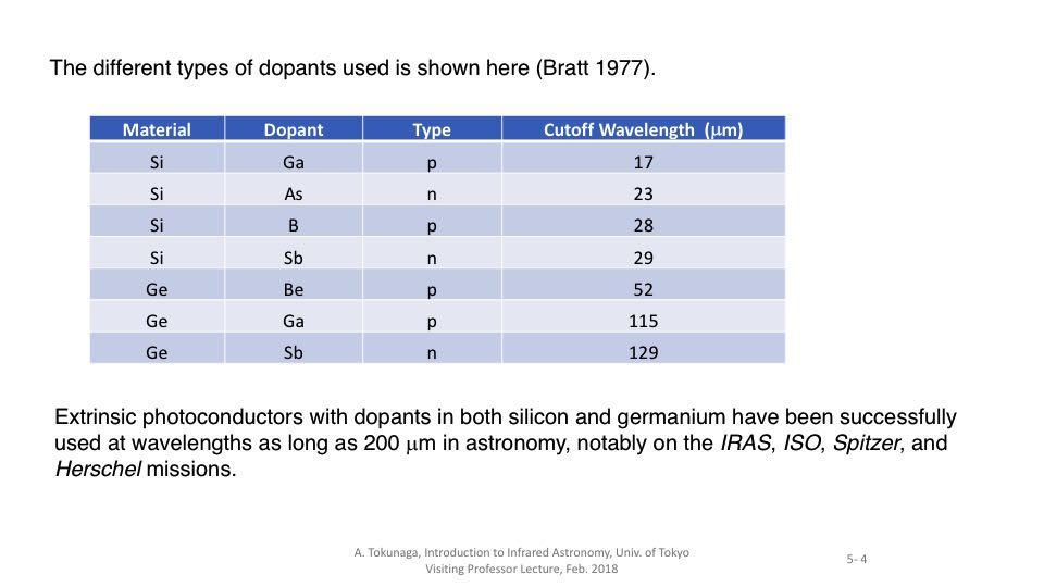
2 Notes: The term intrinsic means the material is pure and the properties measured are intrinsic to the material. Table is from Bratt, P.R. 1977, in Semiconductors and Semimetals, vol. 12, ed. R.K. Willardson & A.C. Beer (New York: Academic), 39. Reference: Rieke, G. H. (2007). "Infrared Detector Arrays for Astronomy." Annual Review of Astronomy and Astrophysics 45: The number of electrons jumping into the conduction band proportional to exp(-e g /2kT), where E g is the energy gap and T is the temperature.
3 Notes:
4 Notes:
5 Notes:
6 Notes: References: Ives, D. et al. (2012). AQUARIUS, the next generation mid-ir detector for ground-based astronomy. High Energy, Optical, and Infrared Detectors for Astronomy V, SPIE, Bharat, R. (1994). "Impurity band conduction detectors for astronomy." Experimental Astronomy 3:
7 Notes: See Rieke (2007) for description of the construction of a detector. The photodiode is the basis for near-infrared detectors such as InSb and HgCdTe.

8 Notes: Figure showing how the long wavelength cut off for HgCdTe can be modified by changing the cadmium fraction in the material.

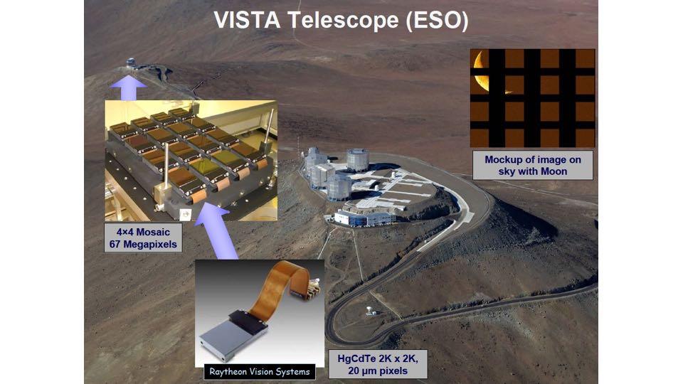
9 Notes: Although a 4Kx4K array was predicted to be achieved about 2004, such engineering-grade arrays were not achieved until 2012 and science-grade arrays about 2015 (D. Hall). This indicates that the practical limits of achieving ever larger arrays has been reached. The high cost of fabricating these arrays is also a factor and very few projects need or can afford larger infrared arrays. Reference: Hoffman, A. W. et al. (2004). Megapixel detector arrays: visible to 28 µm. Focal Plane Arrays for Space Telescopes. SPIE, 5167:
10 Notes:
11 Notes: Detailed discussion of H2RG arrays. Readout, noise, QE. Nearly perfect detector. Use in ground-based and space observatories.

12 Notes: Figure from Beletic et al. (2008) illustrating the technique of bonding a detector array to a readout circuit. Unlike a CCD, each pixel is connected to an amplifier to detect and readout the charge. The reason for this approach is that the readout circuit is constructed out of silicon, while the detector material is made from InSb or HgCdTe. A CCD, on the other hand, can be constructed entirely out of silicon. Indium is used for the electrical connection because it is a soft material and is electrically conducting at low temperatures. Reference: Beletic, J. W. et al. (2008). Teledyne Imaging Sensors: infrared imaging technologies for astronomy and civil space. High Energy, Optical, and Infrared Detectors for Astronomy III., SPIE, 7021, 70210H.

13 Notes: This schematic diagram shows one pixel (one photodiode) of the array and gives you an idea of the complexity of the array construction. The pixel is connected electrically to the readout electronics by an indium bump that is pressed onto the metal contact shown on the left. The active area is only about micrometers thick. The substrate is thinned to maximize throughput. Reference: Rieke, G. H. (2007). "Infrared Detector Arrays for Astronomy." Annual Review of Astronomy and Astrophysics 45:

14 Notes: Reference: Rauscher, B. J. (2015). "Teledyne H1RG, H2RG, and H4RG Noise Generator." Publications of the Astronomical Society of the Pacific 127: In this diagram the photodiode is shown using the standard symbol of a diode plus a parasitic capacitor inherent in any diode. The MOSFET (metal oxide semiconductor field effect transistors) in the circuit are used as switches and as a source follower amplifier. Ørst and Øselect are switches to control the reset voltage applied to the detector and the selection of the detector for reading out. The light blue square represents the photodiode. The location of the indium bump that establishes the electrical connection to the multiplexer is shown. Since MOSFET transistors are used, the signal level can be measured non-destructively. This is a significant factor that allows for the reduction of noise.
15 Notes: This figure shows two MOSFETs as switches.
16 Notes: This figure shows two MOSFETs as switches. It is remarkable that this circuit can operate at temperatures as low as 30K and provide detection down to a 3-5 electrons.
17 Notes:
18 Notes:
19 Notes:
20 Notes:
21 Notes:

22 Notes: Rieke, G. H. (2007). "Infrared Detector Arrays for Astronomy." Annual Review of Astronomy and Astrophysics 45:
23 Notes: This chart shows test results for the JWST NIRSpec H2RG arrays. Note the read noise and dark current. The quantum efficiency is between 0.8 and 1.0. These detectors are therefore nearly ideal. Reference: Rauscher, B. J. et al. (2014). "New and Better Detectors for the JWST Near-Infrared Spectrograph." Publications of the Astronomical Society of the Pacific 126: 739.

24 Notes: Reference: Loose, M. et al. (2003). HAWAII-2RG: a 2k x 2k CMOS multiplexer for low and high background astronomy applications. IR Space Telescopes and Instruments. J. C. Mather, SPIE. 4850:

25 Notes: Reference: Beletic, J. W. et al. (2008). Teledyne Imaging Sensors: infrared imaging technologies for astronomy and civil space. High Energy, Optical, and Infrared Detectors for Astronomy III, SPIE. 7021: 70210H.

26 Notes: Reference: %20Jan_2017_V1.0.pdf This is the specs for a ground-based application. For JWST the SIDECAR ASIC dissipates less the 8 mw of power.
 and the ASIC are cooled inside of the cryostat.")
27 Notes: Reference: %20Jan_2017_V1.0.pdf Blue shaded area shows the cryostat. The detector (SCA) and the ASIC are cooled inside of the cryostat. The ASIC is controlled by the host computer through an interface card called the SIDECAR Acquisition Module.

28 Notes: Image shown is a H2RG array controller built at the NASA Infrared Telescope Facility.

29 Notes: Images from Teledyne and D. Hall.

30 Notes: This slide shows the progression of HdCdTe array development to ever larger arrays and capability (D. Hall, private communication). The principal investigator for these arrays is Donald Hall at the Institute for Astronomy, University of Hawaii. He worked closely with Teledyne Imaging Systems since 1994 to develop these arrays.

31 Notes: Images from Teledyne and D. Hall.

32 Notes: Images from Teledyne and D. Hall.

33 Notes: Photo from D. Hall.
34 Notes:
35 Notes:
Astronomical Techniques I
 Astronomical Techniques I Lecture 8 Yogesh Wadadekar Jan-Feb 2015 IUCAA-NCRA Grad School 1 / 28 Assignment 1 will be posted on the website by tonight or tomorrow morning. Kaustubh Vaghmare (kaustubh@iucaa.ernet.in)
Grand Canyon 8-m Telescope 1929
 1 2 Grand Canyon 8-m Telescope 1929 3 A World-wide Sample of Instruments 4 Instrumentation Details Instrument name Observing Modes Start of operations Wavelength Coverage Field of View Instrument cost
Classification of Solids
 Classification of Solids Classification by conductivity, which is related to the band structure: (Filled bands are shown dark; D(E) = Density of states) Class Electron Density Density of States D(E) Examples
Spitzer Space Telescope
 Spitzer Space Telescope (A.K.A. The Space Infrared Telescope Facility) The Infrared Imaging Chain 1/38 The infrared imaging chain Generally similar to the optical imaging chain... 1) Source (different
Chapter 1 Overview of Semiconductor Materials and Physics
 Chapter 1 Overview of Semiconductor Materials and Physics Professor Paul K. Chu Conductivity / Resistivity of Insulators, Semiconductors, and Conductors Semiconductor Elements Period II III IV V VI 2 B
Detecting Cosmic Rays in Infrared Data
 The 2010 STScI Calibration Workshop Space Telescope Science Institute, 2010 Susana Deustua and Cristina Oliveira, eds. Detecting Cosmic Rays in Infrared Data Rachel E. Anderson and Karl Gordon Space Telescope
CONVERSION GAIN AND INTERPIXEL CAPACITANCE OF CMOS HYBRID FOCAL PLANE ARRAYS Nodal capacitance measurement by a capacitance comparison technique
 CONVERSION GAIN AND INTERPIXEL CAPACITANCE OF CMOS HYBRID FOCAL PLANE ARRAYS Nodal capacitance measurement by a capacitance comparison technique G. Finger 1, J. Beletic 2, R. Dorn 1, M. Meyer 1, L. Mehrgan
The Fantastical Discoveries of Astronomy made possible by the Wonderful Properties of II-VI Materials
 The Fantastical Discoveries of Astronomy made possible by the Wonderful Properties of II-VI Materials Presentation to the Rochester Institute of Technology Virtual Detector Workshop 26 March 2012 James
Atmospheric Extinction
 Atmospheric Extinction Calibrating stellar photometry requires correction for loss of light passing through the atmosphere. Atmospheric Rayleigh and aerosol scattering preferentially redirects blue light
Syllabus: UHH ASTR 450 (F18): Astronomical Instrumentation
: Astronomical Instrumentation") Syllabus: UHH ASTR 450 (F18): Astronomical Instrumentation Prof. Klaus W. Hodapp This course is the final course in the 3-course series on optics and astronomical instrumentation offered at UHH. We will
Syllabus: UHH ASTR 450 (F18): Astronomical Instrumentation Prof. Klaus W. Hodapp This course is the final course in the 3-course series on optics and astronomical instrumentation offered at UHH. We will
I. Introduction II. Solid State Physics Detection of Light Bernhard Brandl 1
 Detection of Light I. Introduction II. Solid State Physics 4-2-2015 Detection of Light Bernhard Brandl 1 4-2-2015 Detection of Light Bernhard Brandl 2 Blabla Recommended 4-2-2015 Detection of Light Bernhard
Mitigation of H2RG persistence with image illumination Brian A. McLeod* a, Roger Smith b
 Mitigation of H2RG persistence with image illumination Brian A McLeod* a, Roger Smith b a Harvard-Smithsonian Center for Astrophysics, 60 Garden St, Cambridge, MA 02138; b Caltech Optical Observatories,
Development of High-Z Semiconductor Detectors and Their Applications to X-ray/gamma-ray Astronomy
 Development of High-Z Semiconductor Detectors and Their Applications to X-ray/gamma-ray Astronomy Taka Tanaka (SLAC/KIPAC) 9/19/2007 SLAC Advanced Instrumentation Seminar Outline Introduction CdTe Diode
ELECTRONIC DEVICES AND CIRCUITS SUMMARY
 ELECTRONIC DEVICES AND CIRCUITS SUMMARY Classification of Materials: Insulator: An insulator is a material that offers a very low level (or negligible) of conductivity when voltage is applied. Eg: Paper,
Detectors for IR astronomy
 Detectors for IR astronomy Where does infrared begin? Wavelength sensi?vity of the human eye vs. wavelength Note: the eye has some (limited) sensi?vity to IR light at ~1000nm (=0.5x energy of photons the
Unit IV Semiconductors Engineering Physics
 Introduction A semiconductor is a material that has a resistivity lies between that of a conductor and an insulator. The conductivity of a semiconductor material can be varied under an external electrical
Electronic Devices & Circuits
 Electronic Devices & Circuits For Electronics & Communication Engineering By www.thegateacademy.com Syllabus Syllabus for Electronic Devices Energy Bands in Intrinsic and Extrinsic Silicon, Carrier Transport,
POSITION SENSITIVE DETECTORS - 8. Dept. Physics & Astronomy
 POSITION SENSITIVE DETECTORS - 8 Optical and IR Applications in Astronomy and Astrophysics Ian S. McLean Dept. Physics & Astronomy University it of California, i Los Angeles INTRODUCTION 400 th anniversary
Interpixel capacitive coupling
 Rochester Institute of Technology RIT Scholar Works Theses Thesis/Dissertation Collections 1-1-2009 Interpixel capacitive coupling Linpeng Cheng Follow this and additional works at: http://scholarworks.rit.edu/theses
3C3 Analogue Circuits
 Department of Electronic & Electrical Engineering Trinity College Dublin, 2014 3C3 Analogue Circuits Prof J K Vij jvij@tcd.ie Lecture 1: Introduction/ Semiconductors & Doping 1 Course Outline (subject
Astr 2310 Thurs. March 3, 2016 Today s Topics
 Astr 2310 Thurs. March 3, 2016 Today s Topics Chapter 6: Telescopes and Detectors Optical Telescopes Simple Optics and Image Formation Resolution and Magnification Invisible Astronomy Ground-based Radio
Astronomical Observing Techniques 2017 Lecture 10: Silicon Eyes 2
 Astronomical Observing Techniques 2017 Lecture 10: Silicon Eyes 2 Christoph U. Keller keller@strw.leidenuniv.nl Content 1. Quantum Efficiency 2. CCD Focal Plane Architectures 3. Readout Noise 4. CCD Data
A semiconductor is an almost insulating material, in which by contamination (doping) positive or negative charge carriers can be introduced.
 positive or negative charge carriers can be introduced.") Semiconductor A semiconductor is an almost insulating material, in which by contamination (doping) positive or negative charge carriers can be introduced. Page 2 Semiconductor materials Page 3 Energy levels
Semiconductor A semiconductor is an almost insulating material, in which by contamination (doping) positive or negative charge carriers can be introduced. Page 2 Semiconductor materials Page 3 Energy levels
Computer modelling of Hg 1 x Cd x Te photodiode performance
 Computer modelling of Hg 1 x Cd x Te photodiode performance Robert Ciupa * Abstract A numerical technique has been used to solve the carrier transport equations for Hg 1-x Cd x Te photodiodes. The model
CMOS Devices and CMOS Hybrid Devices. Array Detector Data Reduction and Problems
 Lecture 12: Image Detectors Outline 1 Overview 2 Photoconductive Detection 3 Charge Coupled Devices 4 CMOS Devices and CMOS Hybrid Devices 5 Array Detector Data Reduction and Problems Overview Photon Detection
EE 446/646 Photovoltaic Devices I. Y. Baghzouz
 EE 446/646 Photovoltaic Devices I Y. Baghzouz What is Photovoltaics? First used in about 1890, the word has two parts: photo, derived from the Greek word for light, volt, relating to electricity pioneer
ITT Technical Institute ET215 Devices I Unit 1
 ITT Technical Institute ET215 Devices I Unit 1 Chapter 1 Chapter 2, Sections 2.1-2.4 Chapter 1 Basic Concepts of Analog Circuits Recall ET115 & ET145 Ohms Law I = V/R If voltage across a resistor increases
EE 5344 Introduction to MEMS CHAPTER 5 Radiation Sensors
 EE 5344 Introduction to MEMS CHAPTER 5 Radiation Sensors 5. Radiation Microsensors Radiation µ-sensors convert incident radiant signals into standard electrical out put signals. Radiant Signals Classification
Lecture 11: Direct Imaging 1. Overview. Photoconductive Detection. Charge Coupled Devices. Outline
 Lecture 11: Direct Imaging 1 Outline 1 Overview 2 Photoconductive Detection 3 Charge Coupled Devices Christoph U. Keller, Utrecht University, C.U.Keller@uu.nl Observational Astrophysics 2, Lecture 11:
CME 300 Properties of Materials. ANSWERS: Homework 9 November 26, As atoms approach each other in the solid state the quantized energy states:
 CME 300 Properties of Materials ANSWERS: Homework 9 November 26, 2011 As atoms approach each other in the solid state the quantized energy states: are split. This splitting is associated with the wave
Flipping Bits in the James Webb Space Telescope s Cameras
 Flipping Bits in the James Webb Space Telescope s Cameras Lance Simms IEEE Life Members Talk 05/16/2018 LLNL-PRES-735208 This work was performed under the auspices of the U.S. Department of Energy by Lawrence
JRA3: Technology development for high-time-resolution astronomy
 JRA3: Technology development for high-time-resolution astronomy ( HTRA: ~ 10 ms -- 1μs ) Objectives: - To develop the most promising technologies for HTRA - Assess relative strengths/areas of application
Peter Fischer, ziti, Universität Heidelberg. Silicon Detectors & Readout Electronics
 Silicon Detectors and Readout Electronics Peter Fischer, ziti, Universität Heidelberg 1 Content of the Lecture (sorted by subject) Introduction: Applications of silicon detectors Requirements, measured
Instrumentation for sub-mm astronomy. Adam Woodcraft SUPA, University of Edinburgh
 Instrumentation for sub-mm astronomy Adam Woodcraft http://woodcraft.lowtemp.org SUPA, University of Edinburgh 1 2 Introduction Sub-mm astronomy 1 Astronomy at sub-mm wavelengths Between infrared and millimetre
EE301 Electronics I , Fall
 EE301 Electronics I 2018-2019, Fall 1. Introduction to Microelectronics (1 Week/3 Hrs.) Introduction, Historical Background, Basic Consepts 2. Rewiev of Semiconductors (1 Week/3 Hrs.) Semiconductor materials
Lecture 2. Introduction to semiconductors Structures and characteristics in semiconductors
 Lecture 2 Introduction to semiconductors Structures and characteristics in semiconductors Semiconductor p-n junction Metal Oxide Silicon structure Semiconductor contact Literature Glen F. Knoll, Radiation
25 Instruments for Optical Spectrometry
 25 Instruments for Optical Spectrometry 25A INSTRUMENT COMPONENTS (1) source of radiant energy (2) wavelength selector (3) sample container (4) detector (5) signal processor and readout (a) (b) (c) Fig.
Introduction to Semiconductor Devices
 Physics 233 Experiment 48 Introduction to Semiconductor Devices References 1. G.W. Neudeck, The PN Junction Diode, Addison-Wesley MA 1989 2. Background notes (Appendix A) 3. Specification sheet for Diode
Lecture 2. Introduction to semiconductors Structures and characteristics in semiconductors
 Lecture 2 Introduction to semiconductors Structures and characteristics in semiconductors Semiconductor p-n junction Metal Oxide Silicon structure Semiconductor contact Literature Glen F. Knoll, Radiation
PHOTOVOLTAICS Fundamentals
 PHOTOVOLTAICS Fundamentals PV FUNDAMENTALS Semiconductor basics pn junction Solar cell operation Design of silicon solar cell SEMICONDUCTOR BASICS Allowed energy bands Valence and conduction band Fermi
Astronomical Observing Techniques 2017 Lecture 9: Silicon Eyes 1
 Astronomical Observing Techniques 2017 Lecture 9: Silicon Eyes 1 Christoph U. Keller keller@strw.leidenuniv.nl Content 1. Detector Types 2. Crystal La>ces 3. Electronic Bands 4. Fermi Energy and Fermi
Conductivity and Semi-Conductors
 Conductivity and Semi-Conductors J = current density = I/A E = Electric field intensity = V/l where l is the distance between two points Metals: Semiconductors: Many Polymers and Glasses 1 Electrical Conduction
Introduction to Semiconductor Devices
 Physics 233 Experiment 48 Introduction to Semiconductor Devices References 1. G.W. Neudeck, The PN Junction Diode, Addison-Wesley MA 1989 2. Background notes (Appendix A) 3. Specification sheet for Diode
Astronomical Observing Techniques Lecture 10: Silicon Eyes 2
 Astronomical Observing Techniques Lecture 10: Silicon Eyes 2 Christoph U. Keller keller@strw.leidenuniv.nl Overview 1. CCD Opera:on 2. CCD Data Reduc:on 3. CMOS devices 4. IR Arrays 5. Bolometers 6. MKIDS
Notes: Reference: Merline, W. J. and S. B. Howell (1995). "A Realistic Model for Point-sources Imaged on Array Detectors: The Model and Initial
. A Realistic Model for Point-sources Imaged on Array Detectors: The Model and Initial") Notes: Notes: Notes: Reference: Merline, W. J. and S. B. Howell (1995). "A Realistic Model for Point-sources Imaged on Array Detectors: The Model and Initial Results." Experimental Astronomy 6: 163-210.
Notes: Notes: Notes: Reference: Merline, W. J. and S. B. Howell (1995). "A Realistic Model for Point-sources Imaged on Array Detectors: The Model and Initial Results." Experimental Astronomy 6: 163-210.
Electric Fields. Basic Concepts of Electricity. Ohm s Law. n An electric field applies a force to a charge. n Charges move if they are mobile
 Basic Concepts of Electricity oltage E Current I Ohm s Law Resistance R E = I R Electric Fields An electric field applies a force to a charge Force on positive charge is in direction of electric field,
1 Name: Student number: DEPARTMENT OF PHYSICS AND PHYSICAL OCEANOGRAPHY MEMORIAL UNIVERSITY OF NEWFOUNDLAND. Fall :00-11:00
 1 Name: DEPARTMENT OF PHYSICS AND PHYSICAL OCEANOGRAPHY MEMORIAL UNIVERSITY OF NEWFOUNDLAND Final Exam Physics 3000 December 11, 2012 Fall 2012 9:00-11:00 INSTRUCTIONS: 1. Answer all seven (7) questions.
Quiz #1 Practice Problem Set
 Name: Student Number: ELEC 3908 Physical Electronics Quiz #1 Practice Problem Set? Minutes January 22, 2016 - No aids except a non-programmable calculator - All questions must be answered - All questions
From here we define metals, semimetals, semiconductors and insulators
 Topic 11-1: Heat and Light for Intrinsic Semiconductors Summary: In this video we aim to discover how intrinsic semiconductors respond to heat and light. We first look at the response of semiconductors
Sensors and Actuators Sensors Physics
 Sensors and Actuators Sensors Physics Sander Stuijk (s.stuijk@tue.nl) Department of Electrical Engineering Electronic Systems HEMOESISIVE SENSOS (Chapter 16.3) 3 emperature sensors placement excitation
NASA Infrared Telescope Facility (IRTF) Alan Tokunaga
 Alan Tokunaga") NASA Infrared Telescope Facility (IRTF) Alan Tokunaga 1 Current status The 3-m IRTF is operated by the University of Hawaii under a a 5-year contract with NASA. 50% of the IRTF time is for solar system
NASA Infrared Telescope Facility (IRTF) Alan Tokunaga 1 Current status The 3-m IRTF is operated by the University of Hawaii under a a 5-year contract with NASA. 50% of the IRTF time is for solar system
ESE370: Circuit-Level Modeling, Design, and Optimization for Digital Systems
 ESE370: Circuit-Level Modeling, Design, and Optimization for Digital Systems Lec 6: September 14, 2015 MOS Model You are Here: Transistor Edition! Previously: simple models (0 and 1 st order) " Comfortable
X- & γ-ray Instrumentation
 X- & γ-ray Instrumentation Used nuclear physics detectors Proportional Counters Scintillators The Dark Ages Simple collimators HEAO A1 & A2: 2 x 8 degree field of view Confusion limit is about 200 sources
Near-infrared guiding and tip-tilt correction for the UC Berkeley Infrared Spatial Interferometer
 Near-infrared guiding and tip-tilt correction for the UC Berkeley Infrared Spatial Interferometer E. A. Lipman, M. Bester, W. C. Danchi, and C. H. Townes Space Sciences Laboratory and Department of Physics
CCD OPERATION. The BBD was an analog delay line, made up of capacitors such that an analog signal was moving along one step at each clock cycle.
 CCDS Lesson 4 CCD OPERATION The predecessor of the CCD was a device called the BUCKET BRIGADE DEVICE developed at the Phillips Research Labs The BBD was an analog delay line, made up of capacitors such
Week 7. Observing happens the week after midterm.
 Week 7 Midterm exam in class next Thursday, March 23 Evening sessions this week are Python data analysis package oriented in support of Lab 3 writeups. Given the interruption for the exam the due date
Uncovering the Early Stages of Galaxy Evolution: Multi-Object Spectrometry with JWST/NIRSpec
 Multi-Object Spectroscopy in the Next Decade: Big Questions, Large Surveys, and Wide Fields ASP Conference Series, Vol. 507 I. Skillen, M. Balcells, and S. C. Trager, eds. c 2016 Astronomical Society of
Advances in Infrared Instrumentation
 Advances in Infrared Instrumentation Dan Jaffe UT Austin Look at the past, present, and future of infrared instrumentation through the lens of high resolution spectroscopy. We are lazy. Most of the gains
Problem Solving. radians. 180 radians Stars & Elementary Astrophysics: Introduction Press F1 for Help 41. f s. picture. equation.
 Problem Solving picture θ f = 10 m s =1 cm equation rearrange numbers with units θ factors to change units s θ = = f sinθ fθ = s / cm 10 m f 1 m 100 cm check dimensions 1 3 π 180 radians = 10 60 arcmin
A 9 megapixel large-area back-thinned CMOS sensor with high sensitivity and high frame-rate for the TAOS II program
 A 9 megapixel large-area back-thinned CMOS sensor with high sensitivity and high frame-rate for the TAOS II program Jérôme Pratlong *a, Shiang-Yu Wang b, Matthew Lehner b, Paul Jorden a, Paul Jerram a,
Engineering 2000 Chapter 8 Semiconductors. ENG2000: R.I. Hornsey Semi: 1
 Engineering 2000 Chapter 8 Semiconductors ENG2000: R.I. Hornsey Semi: 1 Overview We need to know the electrical properties of Si To do this, we must also draw on some of the physical properties and we
Near-infrared InGaAs detectors for background-limited imaging and photometry
 Near-infrared InGaAs detectors for background-limited imaging and photometry The MIT Faculty has made this article openly available. Please share how this access benefits you. Your story matters. Citation
Very long wavelength type-ii InAs/GaSb superlattice infrared detectors
 Very long wavelength type-ii InAs/GaSb superlattice infrared detectors L. Höglund 1, J. B. Rodriguez 2, S. Naureen 1, R. Ivanov 1, C. Asplund 1, R. Marcks von Würtemberg 1, R. Rossignol 2, P. Christol
Radiation Detector 2016/17 (SPA6309)
") Radiation Detector 2016/17 (SPA6309) Semiconductor detectors (Leo, Chapter 10) 2017 Teppei Katori Semiconductor detectors are used in many situations, mostly for some kind of high precision measurement.
Radiation Detector 2016/17 (SPA6309) Semiconductor detectors (Leo, Chapter 10) 2017 Teppei Katori Semiconductor detectors are used in many situations, mostly for some kind of high precision measurement.
Development of sensitive long-wave infrared detector arrays for passively cooled space missions
 Development of sensitive long-wave infrared detector arrays for passively cooled space missions Craig McMurtry Donald Lee James Beletic Chi-Yi A. Chen Richard T. Demers Meghan Dorn Dennis Edwall Candice
Semiconductors and Optoelectronics. Today Semiconductors Acoustics. Tomorrow Come to CH325 Exercises Tours
 Semiconductors and Optoelectronics Advanced Physics Lab, PHYS 3600 Don Heiman, Northeastern University, 2017 Today Semiconductors Acoustics Tomorrow Come to CH325 Exercises Tours Semiconductors and Optoelectronics
Lecture 2. Introduction to semiconductors Structures and characteristics in semiconductors. Fabrication of semiconductor sensor
 Lecture 2 Introduction to semiconductors Structures and characteristics in semiconductors Semiconductor p-n junction Metal Oxide Silicon structure Semiconductor contact Fabrication of semiconductor sensor
XI. Bolometers Principle XII. Bolometers Response. This lecture course follows the textbook Detection of
 Detection of Light XI. Bolometers Principle XII. Bolometers Response This lecture course follows the textbook Detection of Light 23-3-2018 by George Rieke, Detection Cambridge of Light Bernhard Brandl
Semiconductor Optoelectronics Prof. M. R. Shenoy Department of Physics Indian Institute of Technology, Delhi
 Semiconductor Optoelectronics Prof. M. R. Shenoy Department of Physics Indian Institute of Technology, Delhi Lecture - 1 Context and Scope of the Course (Refer Slide Time: 00:44) Welcome to this course
Electrons are shared in covalent bonds between atoms of Si. A bound electron has the lowest energy state.
 Photovoltaics Basic Steps the generation of light-generated carriers; the collection of the light-generated carriers to generate a current; the generation of a large voltage across the solar cell; and
Section 12: Intro to Devices
 Section 12: Intro to Devices Extensive reading materials on reserve, including Robert F. Pierret, Semiconductor Device Fundamentals EE143 Ali Javey Bond Model of Electrons and Holes Si Si Si Si Si Si Si
Telescopes & Instrumentation. Across the Infrared and Submillimetre Wavebands
 Telescopes & Instrumentation Across the Infrared and Submillimetre Wavebands Wayne Holland Lecture for the PPARC Introductory School for new astronomy postgraduate students Edinburgh: 6 th September 2005
Sensing, Computing, Actuating
 Sensing, Computing, Actuating Sander Stuijk (s.stuijk@tue.nl) Department of Electrical Engineering Electronic Systems HEMOESISIVE SENSOS AND LINEAIZAION (Chapter.9, 5.11) 3 Applications discharge air temperature
Device 3D. 3D Device Simulator. Nano Scale Devices. Fin FET
 Device 3D 3D Device Simulator Device 3D is a physics based 3D device simulator for any device type and includes material properties for the commonly used semiconductor materials in use today. The physical
Lecture 1. OUTLINE Basic Semiconductor Physics. Reading: Chapter 2.1. Semiconductors Intrinsic (undoped) silicon Doping Carrier concentrations
 silicon Doping Carrier concentrations") Lecture 1 OUTLINE Basic Semiconductor Physics Semiconductors Intrinsic (undoped) silicon Doping Carrier concentrations Reading: Chapter 2.1 EE105 Fall 2007 Lecture 1, Slide 1 What is a Semiconductor? Low
Lecture 1 OUTLINE Basic Semiconductor Physics Semiconductors Intrinsic (undoped) silicon Doping Carrier concentrations Reading: Chapter 2.1 EE105 Fall 2007 Lecture 1, Slide 1 What is a Semiconductor? Low
Lecture 8. Detectors for Ionizing Particles
 Lecture 8 Detectors for Ionizing Particles Content Introduction Overview of detector systems Sources of radiation Radioactive decay Cosmic Radiation Accelerators Interaction of Radiation with Matter General
Diode Characterization of Rockwell LWIR HgCdTe Detector Arrays
 Diode Characterization of Rockwell LWIR HgCdTe Detector Arrays Candice M. Bacon a, Judith L. Pipher a, William J. Forrest a,craigw.mcmurtry a and James D. Garnett b a University ofrochester, Rochester,
Photonic Communications Engineering Lecture. Dr. Demetris Geddis Department of Engineering Norfolk State University
 Photonic Communications Engineering Lecture Dr. Demetris Geddis Department of Engineering Norfolk State University Light Detectors How does this detector work? Image from visionweb.com Responds to range
Application of Lock-in Thermography for Defect Localisation at Opened and Fully Packaged Single- and Multi-chip Devices
 Application of Lock-in Thermography for Defect Localisation at Opened and Fully Packaged Single- and Multi-chip Devices Christian Schmidt, Frank Altmann, Christian Große Fraunhofer Institute for Mechanics
Auxiliaire d enseignement Nicolas Ayotte
 2012-02-15 GEL 4203 / GEL 7041 OPTOÉLECTRONIQUE Auxiliaire d enseignement Nicolas Ayotte GEL 4203 / GEL 7041 Optoélectronique VI PN JUNCTION The density of charge sign Fixed charge density remaining 2
Semiconductor Physical Electronics
 Semiconductor Physical Electronics Sheng S. Li Department of Electrical Engineering University of Florida Gainesville, Florida Plenum Press New York and London Contents CHAPTER 1. Classification of Solids
Chapter 4: Bonding in Solids and Electronic Properties. Free electron theory
 Chapter 4: Bonding in Solids and Electronic Properties Free electron theory Consider free electrons in a metal an electron gas. regards a metal as a box in which electrons are free to move. assumes nuclei
The Main Point. Familiar Optics. Some Basics. Lecture #8: Astronomical Instruments. Astronomical Instruments:
 Lecture #8: Astronomical Instruments Astronomical Instruments: Optics: Lenses and Mirrors. Detectors. Ground Based Telescopes: Optical, Infrared, and Radio. Space Based Telescopes. Spacecraft Missions.
n N D n p = n i p N A
 Summary of electron and hole concentration in semiconductors Intrinsic semiconductor: E G n kt i = pi = N e 2 0 Donor-doped semiconductor: n N D where N D is the concentration of donor impurity Acceptor-doped
Study of Solder Ball Bump Bonded Hybrid Silicon Pixel Detectors at DESY
 Study of Solder Ball Bump Bonded Hybrid Silicon Pixel Detectors at DESY S. Arab, S. Choudhury, G. Dolinska, K. Hansen, I. Korol, H. Perrey, D. Pitzl, S. Spannagel ( DESY Hamburg ) E. Garutti, M. Hoffmann,
Digital Electronics Part II - Circuits
 Digital Electronics Part - Circuits Dr.. J. Wassell Gates from Transistors ntroduction Logic circuits are non-linear, consequently we will introduce a graphical technique for analysing such circuits The
Because light behaves like a wave, we can describe it in one of two ways by its wavelength or by its frequency.
 Light We can use different terms to describe light: Color Wavelength Frequency Light is composed of electromagnetic waves that travel through some medium. The properties of the medium determine how light
6.012 Electronic Devices and Circuits
 Page 1 of 12 YOUR NAME Department of Electrical Engineering and Computer Science Massachusetts Institute of Technology 6.012 Electronic Devices and Circuits FINAL EXAMINATION Open book. Notes: 1. Unless
The High Definition X-ray Imager (HDXI) Instrument on the Lynx X-Ray Surveyor
 Instrument on the Lynx X-Ray Surveyor") The High Definition X-ray Imager (HDXI) Instrument on the Lynx X-Ray Surveyor Abraham D. Falcone* a, Ralph P. Kraft b, Marshall W. Bautz c, Jessica A. Gaskin d, John A. Mulqueen d, Doug A. Swartz d, for
The High Definition X-ray Imager (HDXI) Instrument on the Lynx X-Ray Surveyor Abraham D. Falcone* a, Ralph P. Kraft b, Marshall W. Bautz c, Jessica A. Gaskin d, John A. Mulqueen d, Doug A. Swartz d, for
Semiconductors. SEM and EDAX images of an integrated circuit. SEM EDAX: Si EDAX: Al. Institut für Werkstoffe der ElektrotechnikIWE
 SEM and EDAX images of an integrated circuit SEM EDAX: Si EDAX: Al source: [Cal 99 / 605] M&D-.PPT, slide: 1, 12.02.02 Classification semiconductors electronic semiconductors mixed conductors ionic conductors
Chapter 3 Basics Semiconductor Devices and Processing
 Chapter 3 Basics Semiconductor Devices and Processing Hong Xiao, Ph. D. www2.austin.cc.tx.us/hongxiao/book.htm Hong Xiao, Ph. D. www2.austin.cc.tx.us/hongxiao/book.htm 1 Objectives Identify at least two
Chi-square is defined as the sum of the square of the (observed values - expected values) divided by the expected values, or
 divided by the expected values, or") 2016 Midterm Exam (100 points total) Name: Astronomy/Planetary Sciences 518/418 Profs. Hinz/Rieke If you need more space, use the reverse side of the relevant page, but let us know by writing (over) at
2016 Midterm Exam (100 points total) Name: Astronomy/Planetary Sciences 518/418 Profs. Hinz/Rieke If you need more space, use the reverse side of the relevant page, but let us know by writing (over) at
! Previously: simple models (0 and 1 st order) " Comfortable with basic functions and circuits. ! This week and next (4 lectures)
 Comfortable with basic functions and circuits. ! This week and next (4 lectures)") ESE370: CircuitLevel Modeling, Design, and Optimization for Digital Systems Lec 6: September 14, 2015 MOS Model You are Here: Transistor Edition! Previously: simple models (0 and 1 st order) " Comfortable
ESE370: CircuitLevel Modeling, Design, and Optimization for Digital Systems Lec 6: September 14, 2015 MOS Model You are Here: Transistor Edition! Previously: simple models (0 and 1 st order) " Comfortable
CBSE PHYSICS QUESTION PAPER (2005)
") CBSE PHYSICS QUESTION PAPER (2005) (i) (ii) All questions are compulsory. There are 30 questions in total. Questions 1 to 8 carry one mark each, Questions 9 to 18 carry two marks each, Question 19 to 27
CBSE PHYSICS QUESTION PAPER (2005) (i) (ii) All questions are compulsory. There are 30 questions in total. Questions 1 to 8 carry one mark each, Questions 9 to 18 carry two marks each, Question 19 to 27
Toward a 1D Device Model Part 1: Device Fundamentals
 Toward a 1D Device Model Part 1: Device Fundamentals Lecture 7 9/29/2011 MIT Fundamentals of Photovoltaics 2.626/2.627 Fall 2011 Prof. Tonio Buonassisi 1 Learning Objectives: Toward a 1D Device Model 1.
Open Access Deformation Analysis of Infrared Detector with Reticulated InSb Pixel Array
 Send Orders for Reprints to reprints@benthamscience.ae The Open Electrical & Electronic Engineering Journal, 2015, 9, 273-277 273 Open Access Deformation Analysis of 128 128 Infrared Detector with Reticulated
Processing of Semiconducting Materials Prof. Pallab Banerji Department of Material Science Indian Institute of Technology, Kharagpur
 Processing of Semiconducting Materials Prof. Pallab Banerji Department of Material Science Indian Institute of Technology, Kharagpur Lecture - 4 Doping in Semiconductors Good morning. Let us start with
Detector R&D in KAPAC
 Detector R&D in KAPAC Hiroyasu Tajima Stanford Linear Accelerator Center Kavli Institute for Particle Astrophysics and Cosmology Outline Compton Camera SOI detector Scintillator Polarimeter Cherenkov Camera
Integrated Circuits & Systems
 Federal University of Santa Catarina Center for Technology Computer Science & Electronics Engineering Integrated Circuits & Systems INE 5442 Lecture 10 MOSFET part 1 guntzel@inf.ufsc.br ual-well Trench-Isolated
EE130: Integrated Circuit Devices
 EE130: Integrated Circuit Devices (online at http://webcast.berkeley.edu) Instructor: Prof. Tsu-Jae King (tking@eecs.berkeley.edu) TA s: Marie Eyoum (meyoum@eecs.berkeley.edu) Alvaro Padilla (apadilla@eecs.berkeley.edu)