Title: Colloidal Quantum Dots Intraband Photodetectors
|
|
|
- Christian Goodman
- 5 years ago
- Views:
Transcription
1 Title: Colloidal Quantum Dots Intraband Photodetectors Authors: Zhiyou Deng, Kwang Seob Jeong, and Philippe Guyot-Sionnest* Supporting Information: I. Considerations on the optimal detectivity of interband or intraband CQDs. The specific detectivity is defined as (1) where R is the responsivity, A is the area, f is the bandwidth and I n is the current noise (A). The responsivity is the number of carriers per second collected per Watt of input power. In a device with a unity gain, (2) where is the quantum efficiency for charge separation, e is the electron charge, is the frequency of light detected and h is Planck s constant. Increasing the gain such as in phototransistors increases the responsivity but the detectivity is not improved since the noise increases by the same gain. The noise is given by many factors, including Johnson noise, 1/f noise, shot noise and thermal background noise. In the shot noise limit, the noise arises from the constant production and recombination of thermal carriers. The rate of thermal carriers produced in a device of area A and thickness 1/ where is the absorption coefficient is 1 (3) where is the carrier lifetime. A thicker device introduces unnecessary noise without increasing the photocurrent. The shot noise associated with G th is then and D* is given by 1 (4) The background limited performance (BLIP) is achieved when the incident background flux is larger than the thermal carrier generation rate, in which case. The 77K cooling requirements for bulk MCT detectors is due to the increase of the carrier density and the dominance of Auger process at higher temperatures. 2 Carrier Lifetime in QDs films: Assuming that there are no traps, carriers that are in the QD films can recombine by geminate recombination of an electron and a hole in a QD in a time 1 or by Auger recombination if there are three or more carriers in the QD. The dots with three carriers have an Auger recombination lifetime of A0. The number of QDs per unit volume is N. For intrinsic interband CQDs and doped (n=2) intraband CQDs, the average number of electrons and holes per dot is such that the carrier geminate recombination lifetime is, and the carrier Auger lifetime is If, the geminate recombination dominates Auger recombination. The Auger lifetime has not yet been measured in the doped HgSe CQDs but it could possibly be much longer than for interband CQDs given the much sparser density of states. Detectivity in the radiative lifetime limit for Interband and Intraband CQDs. In the radiative limit, the lifetime and absorption depth are related through Einstein s A and B coefficients, where a fast radiative lifetime implies a short absorption depth, therefore Eq.4 may be simplified further since the product becomes material independent. The absorption depth is, where V is the volume occupied per nanocrystal and is the peak cross section. The
2 integrated cross section is so that where is the absorption bandwidth and is the wavelength. Then using and, (4) the maximum detectivity becomes (5) In the intrinsic limit, where N 1 and N 2 are the states degeneracy at the lower and higher level. Equation (5) shows that differences between interband and intraband detectivity with quantum dots are going to be small since the density of states of the ground and excited states will be rather similar. With non-radiative processes, the detectivity is lower. Using,. II. k.p Model The 2-band k.p model and an infinite potential well are used to get the energy vs size shown in Fig. S7. 5 The oscillator strength is calculated as, where m 0 is the free electron mass, is the intraband angular frequency, and Z 1S1P is the matrix element taken as ~ <1S z 1P z > 4 where 1S and 1P z are the envelope functions of the particle in the spherical box. Z 1S1P ~ 0.306R where R is the nanoparticle radius. The oscillator strength is shown in Fig.S7. The radiative lifetime is estimated as (CGS units), where here n is now the medium index of refraction (n~ 1.5 for C 2 Cl 4 ) and L is the local field factor where and for C 2 Cl 4. For a 6 nm diameter HgSe dot, the intraband energy is 0.30 ev, (2450 cm -1 ) the oscillator strength is 6.7, and the radiative lifetime is 640 ns in C 2 Cl 4.


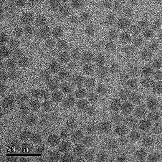
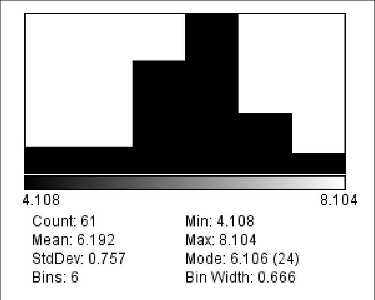
3 Figure S1. TEM image and size analysis of the 1 min sample. Figure S2. TEM image and size analysis of the 4 min sample. Figure S3. TEM image and size analysis of the 16 min sample.
4 Absorption Difference (O.D.) Responsivity (ma/w) Dark current ( A) Figure S4. Responsivity and dark current for a HgSe CQD film under higher bias at 80K Bias (V) Figure S5. Absorption and photocurrent of a HgS CQD film. The absorption (red line) is taken on a ZnSe ATR window at 300K and exhibits the strong intraband absorption. The Photocurrent (PC) (blue line) is taken at 80K. The HgS samples also exhibit a blue shift of the 80K photocurrent compared to the 300 K absorption. The HgS sample is made by reacting. HgCl 2 and thioacetamide in Oleylamine at 35 C for 10 min A -2.2 V 1.0 V V Wavenumber(cm -1 ) 1.0 V 0.6 V 0.2 V V V V Figure S6. Difference absorption spectra of a HgSe CQD film on an evaporated gold slide under electrochemical potential, vs a Ag wire pseudoreference. At increasingly reducing potentials, both the mid-ir intraband absorption and the near-ir interband bleach increase. The sample is pressed against a CaF 2 window to minimize solvent absorption. At the more negative potential, the 1Pe state is charged as evidenced by the interband bleach around 8000 cm -1.
5 Figure S7. Two-band k.p results for the 1S e 1P e transition energy and the oscillator strength. 5 The Kane parameter is E p =18 ev and the bulk gap is chosen to be either -0.1 ev ( red lines, ~ room temperature) or -0.3 ev (blue lines, ~low temperature. E 1Se1Pe (solid lines) and E 1Se (dashed lines) are shown for the two values of the negative gap showing little effect on E 1Se1Pe. The model predicts an intraband transition energy of 0.31 ev (~ 2500 cm -1 ) for a spherical particle of 6 nm diameter, in good agreement with the experimental result. The temperature dependence of E 1Se1Pe is however not explained by this simple model since the change of the gap has apparently little effect. The oscillator strength of the 1S e 1P e transition (black solid line) is shown as well and it is comparable to that of the interband transition (black dashed line). 4 (1) Philipps, J. Evaluation of the Fundamental Properties of Quantum Dot Infrared Detectors, J. Appl. Phys , (2) Chang, Y.; Grein, C. H.; Zhao, J.; Sivananthan, S.; Flatte, M. E.; Liao, P. K.; Aqariden, F. Carrier Recombination Lifetime Characterization of MBE-Grown HgCdTe, Appl. Phys. Lett. 2008, 93, (3) Robel, I.; Gresback, R.; Kortshagen, U.; Klimov, V. I. Universal Size-Dependent Trend in Auger Recombination in Direct-Gap and Indirect-Gap Semiconductor Nanocrystals, Phys Rev Lett. 2009, 102, (4) Khurgin, J. Comparative Analysis of the Intersubband versus Band-to-Band Transitions in Quantum Wells, Appl. Phys. Lett. 1993, 62, 1390 (5) Lhuillier, E.; Keuleyan, S.; Guyot-Sionnest, P. Optical Properties of HgTe Colloidal Quantum Dots. Nanotechnology 2012, 23,
SUPPLEMENTARY INFORMATION
 SUPPLEMENTARY INFORMATION Supplementary Information for Mid-infrared HgTe colloidal quantum dot photodetectors Sean Keuleyan, Emmanuel Lhuillier, Vuk Brajuskovic and Philippe Guyot-Sionnest* Optical absorption
Solar Cell Materials and Device Characterization
 Solar Cell Materials and Device Characterization April 3, 2012 The University of Toledo, Department of Physics and Astronomy SSARE, PVIC Principles and Varieties of Solar Energy (PHYS 4400) and Fundamentals
Computer modelling of Hg 1 x Cd x Te photodiode performance
 Computer modelling of Hg 1 x Cd x Te photodiode performance Robert Ciupa * Abstract A numerical technique has been used to solve the carrier transport equations for Hg 1-x Cd x Te photodiodes. The model
Widely Tunable and Intense Mid-Infrared PL Emission from Epitaxial Pb(Sr)Te Quantum Dots in a CdTe Matrix
Te Quantum Dots in a CdTe Matrix") Widely Tunable and Intense Mid-Infrared PL Emission from Epitaxial Pb(Sr)Te Quantum Dots in a Matrix S. Kriechbaumer 1, T. Schwarzl 1, H. Groiss 1, W. Heiss 1, F. Schäffler 1,T. Wojtowicz 2, K. Koike 3,
Widely Tunable and Intense Mid-Infrared PL Emission from Epitaxial Pb(Sr)Te Quantum Dots in a Matrix S. Kriechbaumer 1, T. Schwarzl 1, H. Groiss 1, W. Heiss 1, F. Schäffler 1,T. Wojtowicz 2, K. Koike 3,
PHOTOVOLTAICS Fundamentals
 PHOTOVOLTAICS Fundamentals PV FUNDAMENTALS Semiconductor basics pn junction Solar cell operation Design of silicon solar cell SEMICONDUCTOR BASICS Allowed energy bands Valence and conduction band Fermi
Luminescence basics. Slide # 1
 Luminescence basics Types of luminescence Cathodoluminescence: Luminescence due to recombination of EHPs created by energetic electrons. Example: CL mapping system Photoluminescence: Luminescence due to
InAs/GaSb Mid-Wave Cascaded Superlattice Light Emitting Diodes
 InAs/GaSb Mid-Wave Cascaded Superlattice Light Emitting Diodes John Prineas Department of Physics and Astronomy, University of Iowa May 3, 206 Collaborator: Thomas Boggess Grad Students: Yigit Aytak Cassandra
Single Photon detectors
 Single Photon detectors Outline Motivation for single photon detection Semiconductor; general knowledge and important background Photon detectors: internal and external photoeffect Properties of semiconductor
Multiple Exciton Generation in Quantum Dots. James Rogers Materials 265 Professor Ram Seshadri
 Multiple Exciton Generation in Quantum Dots James Rogers Materials 265 Professor Ram Seshadri Exciton Generation Single Exciton Generation in Bulk Semiconductors Multiple Exciton Generation in Bulk Semiconductors
Supporting Information
 Supporting Information Remarkable Photothermal Effect of Interband Excitation on Nanosecond Laser-induced Reshaping and Size Reduction of Pseudo-spherical Gold Nanoparticles in Aqueous Solution Daniel
Title: Ultrafast photocurrent measurement of the escape time of electrons and holes from
 Title: Ultrafast photocurrent measurement of the escape time of electrons and holes from carbon nanotube PN junction photodiodes Authors: Nathaniel. M. Gabor 1,*, Zhaohui Zhong 2, Ken Bosnick 3, Paul L.
Evaluation of the fundamental properties of quantum dot infrared detectors
 JOURNAL OF APPLIED PHYSICS VOLUME 91, NUMBER 7 1 APRIL 2002 Evaluation of the fundamental properties of quantum dot infrared detectors Jamie Phillips a) Department of Electrical Engineering and Computer
Chapter 3 The InAs-Based nbn Photodetector and Dark Current
 68 Chapter 3 The InAs-Based nbn Photodetector and Dark Current The InAs-based nbn photodetector, which possesses a design that suppresses surface leakage current, is compared with both a commercially available
A normal-incident quantum well infrared photodetector enhanced by surface plasmon resonance
 Best Student Paper Award A normal-incident quantum well infrared photodetector enhanced by surface plasmon resonance Wei Wu a, Alireza Bonakdar, Ryan Gelfand, and Hooman Mohseni Bio-inspired Sensors and
Quantum confined nanocrystals and nanostructures for high efficiency solar photoconversion Matthew C. Beard
 Quantum confined nanocrystals and nanostructures for high efficiency solar photoconversion Matthew C. Beard NREL is a national laboratory of the U.S. Department of Energy, Office of Energy Efficiency and
Electroluminescence from Silicon and Germanium Nanostructures
 Electroluminescence from silicon Silicon Getnet M. and Ghoshal S.K 35 ORIGINAL ARTICLE Electroluminescence from Silicon and Germanium Nanostructures Getnet Melese* and Ghoshal S. K.** Abstract Silicon
3.1 Introduction to Semiconductors. Y. Baghzouz ECE Department UNLV
 3.1 Introduction to Semiconductors Y. Baghzouz ECE Department UNLV Introduction In this lecture, we will cover the basic aspects of semiconductor materials, and the physical mechanisms which are at the
Transport properties of mid-infrared colloidal quantum dot films
 Transport properties of mid-infrared colloidal quantum dot films Emmanuel Lhuillier, Sean Keuleyan, and Philippe Guyot-Sionnest James Franck Institute, 99 E. 57 th Street, The University of Chicago, Chicago,
DRIFT EFFECTS IN HgCdTe DETECTORS
 Journal of Engineering Science and Technology Vol. 8, No. 4 (2013) 472-481 School of Engineering, Taylor s University DRIFT EFFECTS IN HgCdTe DETECTORS B. PAVAN KUMAR 1, M. W. AKRAM 1, *, BAHNIMAN GHOSH
Efficient Light Scattering in Mid-Infrared Detectors
 Efficient Light Scattering in Mid-Infrared Detectors Arvind P. Ravikumar, Deborah Sivco, and Claire Gmachl Department of Electrical Engineering, Princeton University, Princeton NJ 8544 MIRTHE Summer Symposium
Spectroscopy of. Semiconductors. Luminescence OXFORD IVAN PELANT. Academy ofsciences of the Czech Republic, Prague JAN VALENTA
 Luminescence Spectroscopy of Semiconductors IVAN PELANT Institute ofphysics, v.v.i. Academy ofsciences of the Czech Republic, Prague JAN VALENTA Department of Chemical Physics and Optics Charles University,
Optical Properties of Solid from DFT
 Optical Properties of Solid from DFT 1 Prof.P. Ravindran, Department of Physics, Central University of Tamil Nadu, India & Center for Materials Science and Nanotechnology, University of Oslo, Norway http://folk.uio.no/ravi/cmt15
R.Yang, L.M.Wei and G.L.Yu
 Weak antilocalization effect in LPE-grown p-hg 0.8 Cd 0.2 Te thin film and the evidence of Te-precipitation R.Yang, L.M.Wei and G.L.Yu National Laboratory for Infrared Physics, Shanghai Institute of Technical
REPORT DOCUMENTATION PAGE
 REPORT DOCUMENTATION PAGE Form Approved OMB NO. 0704-0188 Public Reporting burden for this collection of information is estimated to average 1 hour per response, including the time for reviewing instructions,
Growth optimization of InGaAs quantum wires for infrared photodetector applications
 Growth optimization of InGaAs quantum wires for infrared photodetector applications Chiun-Lung Tsai, Chaofeng Xu, K. C. Hsieh, and K. Y. Cheng a Department of Electrical and Computer Engineering and Micro
Thermionic Current Modeling and Equivalent Circuit of a III-V MQW P-I-N Photovoltaic Heterostructure
 Thermionic Current Modeling and Equivalent Circuit of a III-V MQW P-I-N Photovoltaic Heterostructure ARGYRIOS C. VARONIDES Physics and Electrical Engineering Department University of Scranton 800 Linden
Two-photon Absorption Process in Semiconductor Quantum Dots
 Two-photon Absorption Process in Semiconductor Quantum Dots J. López Gondar 1, R. Cipolatti 1 and G. E. Marques 2. 1 Instituto de Matemática, Universidade Federal do Rio de Janeiro C.P. 68530, Rio de Janeiro,
SUPPLEMENTARY INFORMATION
 SUPPLEMENTARY INFORMATION DOI: 10.1038/NNANO.2012.63 Bright infrared quantum-dot light-emitting diodes through inter-dot spacing control Liangfeng Sun, Joshua J. Choi, David Stachnik, Adam C. Bartnik,
Lecture 15: Optoelectronic devices: Introduction
 Lecture 15: Optoelectronic devices: Introduction Contents 1 Optical absorption 1 1.1 Absorption coefficient....................... 2 2 Optical recombination 5 3 Recombination and carrier lifetime 6 3.1
Semiconductor device structures are traditionally divided into homojunction devices
 0. Introduction: Semiconductor device structures are traditionally divided into homojunction devices (devices consisting of only one type of semiconductor material) and heterojunction devices (consisting
Optical Characterization of Self-Assembled Si/SiGe Nano-Structures
 Optical Characterization of Self-Assembled Si/SiGe Nano-Structures T. Fromherz, W. Mac, G. Bauer Institut für Festkörper- u. Halbleiterphysik, Johannes Kepler Universität Linz, Altenbergerstraße 69, A-
Physics of Semiconductors
 Physics of Semiconductors 9 th 2016.6.13 Shingo Katsumoto Department of Physics and Institute for Solid State Physics University of Tokyo Site for uploading answer sheet Outline today Answer to the question
Supplementary Figure 1. Supplementary Figure 1 Characterization of another locally gated PN junction based on boron
 Supplementary Figure 1 Supplementary Figure 1 Characterization of another locally gated PN junction based on boron nitride and few-layer black phosphorus (device S1). (a) Optical micrograph of device S1.
SUPPLEMENTARY INFORMATION
 In the format provided by the authors and unedited. DOI: 10.1038/NNANO.2017.46 Position dependent and millimetre-range photodetection in phototransistors with micrometre-scale graphene on SiC Biddut K.
OPTI510R: Photonics. Khanh Kieu College of Optical Sciences, University of Arizona Meinel building R.626
 OPTI510R: Photonics Khanh Kieu College of Optical Sciences, University of Arizona kkieu@optics.arizona.edu Meinel building R.626 Announcements Homework #6 is assigned, due May 1 st Final exam May 8, 10:30-12:30pm
Light emission from strained germanium
 Light emission from strained germanium Supplementary information P. Boucaud, 1, a) M. El Kurdi, 1 S. Sauvage, 1 M. de Kersauson, 1 A. Ghrib, 1 and X. Checoury 1 Institut d Electronique Fondamentale, CNRS
ET3034TUx Utilization of band gap energy
 ET3034TUx - 3.3.1 - Utilization of band gap energy In the last two weeks we have discussed the working principle of a solar cell and the external parameters that define the performance of a solar cell.
Supplementary Materials
 Supplementary Materials Sample characterization The presence of Si-QDs is established by Transmission Electron Microscopy (TEM), by which the average QD diameter of d QD 2.2 ± 0.5 nm has been determined
Comparison of Ge, InGaAs p-n junction solar cell
 ournal of Physics: Conference Series PAPER OPEN ACCESS Comparison of Ge, InGaAs p-n junction solar cell To cite this article: M. Korun and T. S. Navruz 16. Phys.: Conf. Ser. 77 135 View the article online
Supplementary Information for. Vibrational Spectroscopy at Electrolyte Electrode Interfaces with Graphene Gratings
 Supplementary Information for Vibrational Spectroscopy at Electrolyte Electrode Interfaces with Graphene Gratings Supplementary Figure 1. Simulated from pristine graphene gratings at different Fermi energy
Utmost response time of long-wave HgCdTe photodetectors operating under zero voltage condition
 Opt Quant Electron (2018) 50:17 https://doi.org/10.1007/s11082-017-1278-y Utmost response time of long-wave HgCdTe photodetectors operating under zero voltage condition P. Martyniuk 1 P. Madejczyk 1 M.
Intraband emission of GaN quantum dots at λ =1.5 μm via resonant Raman scattering
 Intraband emission of GaN quantum dots at λ =1.5 μm via resonant Raman scattering L. Nevou, F. H. Julien, M. Tchernycheva, J. Mangeney Institut d Electronique Fondamentale, UMR CNRS 8622, University Paris-Sud
Optically-Pumped Ge-on-Si Gain Media: Lasing and Broader Impact
 Optically-Pumped Ge-on-Si Gain Media: Lasing and Broader Impact J. Liu 1, R. Camacho 2, X. Sun 2, J. Bessette 2, Y. Cai 2, X. X. Wang 1, L. C. Kimerling 2 and J. Michel 2 1 Thayer School, Dartmouth College;
THE DEVELOPMENT OF SIMULATION MODEL OF CARRIER INJECTION IN QUANTUM DOT LASER SYSTEM
 THE DEVELOPMENT OF SIMULATION MODEL OF CARRIER INJECTION IN QUANTUM DOT LASER SYSTEM Norbaizura Nordin 1 and Shahidan Radiman 2 1 Centre for Diploma Studies Universiti Tun Hussein Onn Malaysia 1,2 School
Self-Assembled InAs Quantum Dots
 Self-Assembled InAs Quantum Dots Steve Lyon Department of Electrical Engineering What are semiconductors What are semiconductor quantum dots How do we make (grow) InAs dots What are some of the properties
EE 6313 Homework Assignments
 EE 6313 Homework Assignments 1. Homework I: Chapter 1: 1.2, 1.5, 1.7, 1.10, 1.12 [Lattice constant only] (Due Sept. 1, 2009). 2. Homework II: Chapter 1, 2: 1.17, 2.1 (a, c) (k = π/a at zone edge), 2.3
Optimizing the performance of metal-semiconductor-metal photodetectors by embedding nanoparticles in the absorption layer
 Journal of Electrical and Electronic Engineering 2015; 3(2-1): 78-82 Published online February 10, 2015 (http://www.sciencepublishinggroup.com/j/jeee) doi: 10.11648/j.jeee.s.2015030201.27 ISSN: 2329-1613
Optical Properties of Semiconductors. Prof.P. Ravindran, Department of Physics, Central University of Tamil Nadu, India
 Optical Properties of Semiconductors 1 Prof.P. Ravindran, Department of Physics, Central University of Tamil Nadu, India http://folk.uio.no/ravi/semi2013 Light Matter Interaction Response to external electric
CHAPTER 3. OPTICAL STUDIES ON SnS NANOPARTICLES
 42 CHAPTER 3 OPTICAL STUDIES ON SnS NANOPARTICLES 3.1 INTRODUCTION In recent years, considerable interest has been shown on semiconducting nanostructures owing to their enhanced optical and electrical
Practical 1P4 Energy Levels and Band Gaps
 Practical 1P4 Energy Levels and Band Gaps What you should learn from this practical Science This practical illustrates some of the points from the lecture course on Elementary Quantum Mechanics and Bonding
Carrier Recombination
 Notes for ECE-606: Spring 013 Carrier Recombination Professor Mark Lundstrom Electrical and Computer Engineering Purdue University, West Lafayette, IN USA lundstro@purdue.edu /19/13 1 carrier recombination-generation
MODAL GAIN AND CURRENT DENSITY RELATIONSHIP FOR PbSe/PbSrSe QUANTUM WELL NORMAL AND OBLIQUE DEGENERATE VALLEYS
 Far East Journal of Electronics and Communications 17 Pushpa Publishing House, Allahabad, India http://www.pphmj.com http://dx.doi.org/1.17654/ec1761319 Volume 17, Number 6, 17, Pages 1319-136 ISSN: 973-76
Practical 1P4 Energy Levels and Band Gaps
 Practical 1P4 Energy Levels and Band Gaps What you should learn from this practical Science This practical illustrates some of the points from the lecture course on Elementary Quantum Mechanics and Bonding
Photonic Communications Engineering Lecture. Dr. Demetris Geddis Department of Engineering Norfolk State University
 Photonic Communications Engineering Lecture Dr. Demetris Geddis Department of Engineering Norfolk State University Light Detectors How does this detector work? Image from visionweb.com Responds to range
Infrared Fluorescence of Lead Selenide Colloidal Quantum Dots
 Infrared Fluorescence of Lead Selenide Colloidal Quantum Dots Heng Liu Email: liuh@uchicago.edu Advisor: Philippe Guyot-Sionnest The photoluminescence (PL) of PbSe colloidal quantum dots (QD) is investigated.
Solar cells operation
 Solar cells operation photovoltaic effect light and dark V characteristics effect of intensity effect of temperature efficiency efficency losses reflection recombination carrier collection and quantum
THz Spectroscopy of Nanoscale Materials
 THz Spectroscopy of Nanoscale Materials Frontiers of THz Science Stanford, Sept. 5, 2012 Tony F. Heinz Columbia University New York, NY 10027 http://heinz.phys.columbia.edu tony.heinz@columbia.edu Thanks
Size-Dependent Biexciton Quantum Yields and Carrier Dynamics of Quasi-
 Supporting Information Size-Dependent Biexciton Quantum Yields and Carrier Dynamics of Quasi- Two-Dimensional Core/Shell Nanoplatelets Xuedan Ma, Benjamin T. Diroll, Wooje Cho, Igor Fedin, Richard D. Schaller,
Barrier Photodetectors for High Sensitivity and High Operating Temperature Infrared Sensors
 Barrier Photodetectors for High Sensitivity and High Operating Temperature Infrared Sensors Philip Klipstein General Review of Barrier Detectors 1) Higher operating temperature, T OP 2) Higher signal to
Optical Characteristics of ZnO Based Photodetectors Doped with Au Nanoparticles
 nd International Conference on Mechanical and Electronics Engineering (ICMEE ) Optical Characteristics of ZnO Based Photodetectors Doped with Au Nanoparticles S. Mohammadnejad, S. G. Samani, and E. Rahimi
Uniform excitation: applied field and optical generation. Non-uniform doping/excitation: diffusion, continuity
 6.012 - Electronic Devices and Circuits Lecture 2 - Uniform Excitation; Non-uniform conditions Announcements Review Carrier concentrations in TE given the doping level What happens above and below room
Impact Ionization Can Explain Carrier Multiplication in PbSe Quantum Dots
 Impact Ionization Can Explain Carrier Multiplication in PbSe Quantum Dots A. Franceschetti,* J. M. An, and A. Zunger National Renewable Energy Laboratory, Golden, Colorado 8040 Received May 3, 2006; Revised
Semiconductor Quantum Structures And Energy Conversion. Itaru Kamiya Toyota Technological Institute
 Semiconductor Quantum Structures And nergy Conversion April 011, TTI&NCHU Graduate, Special Lectures Itaru Kamiya kamiya@toyota-ti.ac.jp Toyota Technological Institute Outline 1. Introduction. Principle
Solar Cells Based on. Quantum Dots: Multiple Exciton Generation and Intermediate Bands Antonio Luque, Antonio Marti, and Arthur J.
 Solar Cells Based on Quantum Dots: Multiple Exciton Generation and Intermediate Bands Antonio Luque, Antonio Marti, and Arthur J. Nozik Student ID: 2004171039 Name: Yo-Han Choi Abstract Semiconductor quantum
Study of Minority Carrier Lifetime and Transport in InAs/InAsSb type-ii Superlattices. Using a Real-Time Baseline Correction Method.
 Study of Minority Carrier Lifetime and Transport in InAs/InAsSb type-ii Superlattices Using a Real-Time Baseline Correction Method by Zhiyuan Lin A Dissertation Presented in Partial Fulfillment of the
Implementation of 3D model for generation of simulated EQE spectra
 Supporting information Implementation of 3D model for generation of simulated EQE spectra The EQE can be simulated from EQE R taking into account the filtering of photons through ZnSe and the collection
sin[( t 2 Home Problem Set #1 Due : September 10 (Wed), 2008
, 2008") Home Problem Set #1 Due : September 10 (Wed), 008 1. Answer the following questions related to the wave-particle duality. (a) When an electron (mass m) is moving with the velocity of υ, what is the wave
Home Problem Set #1 Due : September 10 (Wed), 008 1. Answer the following questions related to the wave-particle duality. (a) When an electron (mass m) is moving with the velocity of υ, what is the wave
February 1, 2011 The University of Toledo, Department of Physics and Astronomy SSARE, PVIC
 FUNDAMENTAL PROPERTIES OF SOLAR CELLS February 1, 2011 The University of Toledo, Department of Physics and Astronomy SSARE, PVIC Principles and Varieties of Solar Energy (PHYS 4400) and Fundamentals of
Nanomaterials for Photovoltaics (v11) 14. Intermediate-Band Solar Cells
 14. Intermediate-Band Solar Cells") 1 14. Intermediate-Band Solar Cells Intermediate (impurity) band solar cells (IBSCs) (I) Concept first proposed by A. Luque and A. Martí in 1997. Establish an additional electronic band within the band
1 14. Intermediate-Band Solar Cells Intermediate (impurity) band solar cells (IBSCs) (I) Concept first proposed by A. Luque and A. Martí in 1997. Establish an additional electronic band within the band
Fall 2014 Nobby Kobayashi (Based on the notes by E.D.H Green and E.L Allen, SJSU) 1.0 Learning Objectives
 1.0 Learning Objectives") University of California at Santa Cruz Electrical Engineering Department EE-145L: Properties of Materials Laboratory Lab 7: Optical Absorption, Photoluminescence Fall 2014 Nobby Kobayashi (Based on the
University of California at Santa Cruz Electrical Engineering Department EE-145L: Properties of Materials Laboratory Lab 7: Optical Absorption, Photoluminescence Fall 2014 Nobby Kobayashi (Based on the
Resonant cavity enhancement in heterojunction GaAsÕAlGaAs terahertz detectors
 JOURNAL OF APPLIED PHYSICS VOLUME 93, NUMBER 4 15 FEBRUARY 2003 Resonant cavity enhancement in heterojunction GaAsÕAlGaAs terahertz detectors D. G. Esaev, S. G. Matsik, M. B. M. Rinzan, and A. G. U. Perera
DEVICE CHARACTERISTICS OF VLWIR MCT PHOTODIODES. August 1999
 Approved for public release; distribution is unlimited. DEVICE CHARACTERISTICS OF VLWIR MCT PHOTODIODES August 1999 R.E. DeWames, P.S. Wijewarnasuriya, W. McLevige, D. Edwall, G. Hildebrandt, and J.M.
1) Institut d Electronique Fondamentale, CNRS, Univ. Paris- Sud, Université Paris- Saclay, Bâtiment 220, Rue André Ampère, F Orsay, France
 Institut d Electronique Fondamentale, CNRS, Univ. Paris- Sud, Université Paris- Saclay, Bâtiment 220, Rue André Ampère, F Orsay, France") Supporting information Direct band gap germanium microdisks obtained with silicon nitride stressor layers Moustafa El Kurdi, 1 Mathias Prost, 1 Abdelhamid Ghrib, 1 Sébastien Sauvage, 1 Xavier Checoury,
Supporting information Direct band gap germanium microdisks obtained with silicon nitride stressor layers Moustafa El Kurdi, 1 Mathias Prost, 1 Abdelhamid Ghrib, 1 Sébastien Sauvage, 1 Xavier Checoury,
Optical and Terahertz Characterization of Be-Doped GaAs/AlAs Multiple Quantum Wells
 Vol. 107 (2005) ACTA PHYSICA POLONICA A No. 2 Proceedings of the 12th International Symposium UFPS, Vilnius, Lithuania 2004 Optical and Terahertz Characterization of Be-Doped GaAs/AlAs Multiple Quantum
Defense Technical Information Center Compilation Part Notice
 UNCLASSIFIED Defense Technical Information Center Compilation Part Notice ADP013123 TITLE: The Effect of Deuterium on the Optical Properties of Free Standing Porous Silicon Layers DISTRIBUTION: Approved
Variation of Electronic State of CUBOID Quantum Dot with Size
 Nano Vision, Vol.1 (1), 25-33 (211) Variation of Electronic State of CUBOID Quantum Dot with Size RAMA SHANKER YADAV and B. S. BHADORIA* Department of Physics, Bundelkhand University, Jhansi-284128 U.P.
Chapter 2 Optical Transitions
 Chapter 2 Optical Transitions 2.1 Introduction Among energy states, the state with the lowest energy is most stable. Therefore, the electrons in semiconductors tend to stay in low energy states. If they
MASSACHUSETTS INSTITUTE OF TECHNOLOGY Department of Electrical Engineering And Computer Science Semiconductor Optoelectronics Fall 2002
 MASSACHUSETTS INSTITUTE OF TECHNOLOGY Department of Electrical Engineering And Computer Science 6.977 Semiconductor Optoelectronics Fall 2002 Problem Set 1 Semiconductor electronics Problem #1 The purpose
Plasmonics. The long wavelength of light ( μm) creates a problem for extending optoelectronics into the nanometer regime.
 creates a problem for extending optoelectronics into the nanometer regime.") Plasmonics The long wavelength of light ( μm) creates a problem for extending optoelectronics into the nanometer regime. A possible way out is the conversion of light into plasmons. They have much shorter
Plasmonics The long wavelength of light ( μm) creates a problem for extending optoelectronics into the nanometer regime. A possible way out is the conversion of light into plasmons. They have much shorter
Optical Nonlinearities in Quantum Wells
 Harald Schneider Institute of Ion-Beam Physics and Materials Research Semiconductor Spectroscopy Division Rosencher s Optoelectronic Day Onéra 4.05.011 Optical Nonlinearities in Quantum Wells Harald Schneider
In this block the two transport mechanisms will be discussed: diffusion and drift.
 ET3034TUx - 2.3.3 Transport of charge carriers What are the charge carrier transport principles? In this block the two transport mechanisms will be discussed: diffusion and drift. We will discuss that
Optical properties of wurtzite and zinc-blende GaNÕAlN quantum dots
 Optical properties of wurtzite and zinc-blende GaNÕAlN quantum dots Vladimir A. Fonoberov a) and Alexander A. Balandin b) Nano-Device Laboratory, Department of Electrical Engineering, University of California
Resonator Fabrication for Cavity Enhanced, Tunable Si/Ge Quantum Cascade Detectors
 Resonator Fabrication for Cavity Enhanced, Tunable Si/Ge Quantum Cascade Detectors M. Grydlik 1, P. Rauter 1, T. Fromherz 1, G. Bauer 1, L. Diehl 2, C. Falub 2, G. Dehlinger 2, H. Sigg 2, D. Grützmacher
Recombination: Depletion. Auger, and Tunnelling
 Recombination: Depletion Region, Bulk, Radiative, Auger, and Tunnelling Ch 140 Lecture Notes #13 Prepared by David Gleason We assume: Review of Depletion Region Recombination Flat Quantum Fermi Levels
Intensity / a.u. 2 theta / deg. MAPbI 3. 1:1 MaPbI 3-x. Cl x 3:1. Supplementary figures
 Intensity / a.u. Supplementary figures 110 MAPbI 3 1:1 MaPbI 3-x Cl x 3:1 220 330 0 10 15 20 25 30 35 40 45 2 theta / deg Supplementary Fig. 1 X-ray Diffraction (XRD) patterns of MAPbI3 and MAPbI 3-x Cl
Investigation of Optical Nonlinearities and Carrier Dynamics in In-Rich InGaN Alloys
 Vol. 113 (2008) ACTA PHYSICA POLONICA A No. 3 Proceedings of the 13th International Symposium UFPS, Vilnius, Lithuania 2007 Investigation of Optical Nonlinearities and Carrier Dynamics in In-Rich InGaN
interband transitions in semiconductors M. Fox, Optical Properties of Solids, Oxford Master Series in Condensed Matter Physics
 interband transitions in semiconductors M. Fox, Optical Properties of Solids, Oxford Master Series in Condensed Matter Physics interband transitions in quantum wells Atomic wavefunction of carriers in
TRANSIENT PUMP PROBE ABSORPTION SPECTROSCOPY OF SEMICONDUCTOR NANOTETRAPODS
 TRANSIENT PUMP PROBE ABSORPTION SPECTROSCOPY OF SEMICONDUCTOR NANOTETRAPODS Mikhail LEONOV, 1 Ivan RUKHLENKO, 1,2 Roman NOSKOV, 1,3 Alexander BARANOV, 1 Yurii GUN'KO, 1,4 and Anatoly FEDOROV 1 1 ITMO University,
Graphene photodetectors with ultra-broadband and high responsivity at room temperature
 SUPPLEMENTARY INFORMATION DOI: 10.1038/NNANO.2014.31 Graphene photodetectors with ultra-broadband and high responsivity at room temperature Chang-Hua Liu 1, You-Chia Chang 2, Ted Norris 1.2* and Zhaohui
Physics and Material Science of Semiconductor Nanostructures
 Physics and Material Science of Semiconductor Nanostructures PHYS 570P Prof. Oana Malis Email: omalis@purdue.edu Course website: http://www.physics.purdue.edu/academic_programs/courses/phys570p/ 1 Introduction
Plasmonic Photovoltaics Harry A. Atwater California Institute of Technology
 Plasmonic Photovoltaics Harry A. Atwater California Institute of Technology Surface plasmon polaritons and localized surface plasmons Plasmon propagation and absorption at metal-semiconductor interfaces
Tianle Guo, 1 Siddharth Sampat, 1 Kehao Zhang, 2 Joshua A. Robinson, 2 Sara M. Rupich, 3 Yves J. Chabal, 3 Yuri N. Gartstein, 1 and Anton V.
 SUPPLEMENTARY INFORMATION for Order of magnitude enhancement of monolayer MoS photoluminescence due to near-field energy influx from nanocrystal films Tianle Guo, Siddharth Sampat, Kehao Zhang, Joshua
Introduction to Sources: Radiative Processes and Population Inversion in Atoms, Molecules, and Semiconductors Atoms and Molecules
 OPTI 500 DEF, Spring 2012, Lecture 2 Introduction to Sources: Radiative Processes and Population Inversion in Atoms, Molecules, and Semiconductors Atoms and Molecules Energy Levels Every atom or molecule
Optical and Photonic Glasses. Lecture 39. Non-Linear Optical Glasses III Metal Doped Nano-Glasses. Professor Rui Almeida
 Optical and Photonic Glasses : Non-Linear Optical Glasses III Metal Doped Nano-Glasses Professor Rui Almeida International Materials Institute For New Functionality in Glass Lehigh University Metal-doped
EE 5344 Introduction to MEMS CHAPTER 5 Radiation Sensors
 EE 5344 Introduction to MEMS CHAPTER 5 Radiation Sensors 5. Radiation Microsensors Radiation µ-sensors convert incident radiant signals into standard electrical out put signals. Radiant Signals Classification
MODELING THE FUNDAMENTAL LIMIT ON CONVERSION EFFICIENCY OF QD SOLAR CELLS
 MODELING THE FUNDAMENTAL LIMIT ON CONVERSION EFFICIENCY OF QD SOLAR CELLS Ա.Մ.Կեչիյանց Ara Kechiantz Institute of Radiophysics and Electronics (IRPhE), National Academy of Sciences (Yerevan, Armenia) Marseille
Ge/Si Photodiodes with Embedded Arrays of Ge Quantum Dots for the Near Infrared ( mm) Region
 Region") Semiconductors, Vol. 37, No., 2003, pp. 345 349. Translated from Fizika i Tekhnika Poluprovodnikov, Vol. 37, No., 2003, pp. 383 388. Original Russian Text Copyright 2003 by Yakimov, Dvurechenskiœ, Nikiforov,
Semiconductors, Vol. 37, No., 2003, pp. 345 349. Translated from Fizika i Tekhnika Poluprovodnikov, Vol. 37, No., 2003, pp. 383 388. Original Russian Text Copyright 2003 by Yakimov, Dvurechenskiœ, Nikiforov,
As our population continues to grow, I believe that efficiently harnessing clean, abundant solar energy
 Link Foundation Energy Fellowship Report for Adam Brewer Introduction As our population continues to grow, I believe that efficiently harnessing clean, abundant solar energy would be a tremendous boon
Physics and Material Science of Semiconductor Nanostructures
 Physics and Material Science of Semiconductor Nanostructures PHYS 570P Prof. Oana Malis Email: omalis@purdue.edu Course website: http://www.physics.purdue.edu/academic_programs/courses/phys570p/ 1 Course
Single Emitter Detection with Fluorescence and Extinction Spectroscopy
 Single Emitter Detection with Fluorescence and Extinction Spectroscopy Michael Krall Elements of Nanophotonics Associated Seminar Recent Progress in Nanooptics & Photonics May 07, 2009 Outline Single molecule