Electromagnetic sensors for biomedical and telecommunications applications
|
|
|
- Buddy Jones
- 6 years ago
- Views:
Transcription
 Co-advisor: Prof.")
1 DOTTORATO DI RICERCA IN Ingegneria Sezione: Elettronica Biomedica, dell Elettromagnetismo e delle Telecomunicazioni Electromagnetic sensors for biomedical and telecommunications applications XXVI CICLO DEL CORSO DI DOTTORATO Dottorando: Luigi La Spada Advisor: Prof. Lucio Vegni (Università degli studi Roma Tre, Italia) Co-advisor: Prof. Nader Engheta (University of Pennsylvania, USA) Roma, 15 Maggio 2014
2 Contents CAP 1 Introduction to Metamaterials 01 Introduction 01 Applications of Negative Materials 06 Applications of ENZ and MNZ Materials 08 Conclusions 09 References 10 CAP 2 High sensibility and sensitivity sensors Metasurfaces 17 Introduction The sensing system operation pattern Metamaterials as sensors Geometrical Inductance Geometrical Capacitance Additional Capacitance and Inductance Comparison between analytical and numerical models Selectivity and sensitivity analysis Selectivity analysis Sensitivity analysis Metamaterials for medical diagnostics Permittivity Measurements 33 Cancer stage detection 34 Recognition of organic/inorganic compounds in water solutions Absorption Measurements 36 Diagnosis of healthy, malignant tissues and different cancer stages 37 Water content detection in biological tissue 39 Oxyhaemoglobin and Deoxygenated haemoglobin detection Conclusions 41 References 42
3 CAP 3 High sensibility and sensitivity sensors Nanoparticles 48 Abstract 48 Introduction SPR-based Sensors LSPR-based Sensors Nanoparticles Inter-Coupling effect Structural Modification for Higher Sensitivity Polarizability enhancement by using Multipolar Resonance The Use of Plasmon Hybridization for Enhancing LSPR Resonances Sensitivity Improvement Utilizing Fano Resonance and Symmetry breaking Sensitivity Improvement and Multi resonant structures by using Mixing Formulas and Homogenization Theory 74 Case 1: Inclusions with Lorentz dispersion model in a dispersionless and lossless environment 75 Case 2 Inclusions and environment with Lorentz dispersion model Sensitivity improvement by combining Plasmonics and Epsilon-Near-Zero (ENZ) materials Comparison between Analytical Model, Numerical and Experimental Values Effect of Geometrical and Electromagnetic Parameters and Sensitivity Nanoparticles for medical diagnostics 89 Chemical measurements: detection of glycerol or glucose concentration in aqueous solution 91 Blood diseases detection and tumor recognition 94 Cancer tissue diagnostics 95 Skin diseases diagnostics Conclusions 97 References 98
4 CAP 4 Design of new electromagnetic absorbers and antennas by using Epsilon- Near-Zero Materials 108 Introduction 108 Metamaterial Electromagnetic Wave Absorbers Electromagnetic Wave Absorbers: resonant absorbers and broadband absorbers 109 Resonant Absorbers 109 Broadband Absorbers Metamaterial perfect absorber 111 Perfect Metamaterial Absorbers state of the art Other electromagnetic wave absorbers: plasmons, nanoparticles, subwavelength hole arrays, gratings 119 Plasmons 119 Nanoparticles 119 Subwavelength Hole Arrays 119 Gratings 120 Non-Traditional metamaterial-based absorbers Epsilon-Near-Zero electromagnetic wave absorbers The ENZ absorber 122 Electromagnetic absorption properties of Epsilon-Near-Zero Absorbers: comparison among Metamaterial Perfect Absorbers, Other Electromagnetic Wave Absorbers, and Epsilon-Near-Zero Absorbers 126 Effect of geometrical parameters 126 Effect of electromagnetic characteristics 127 The multi-layered structure Conclusions Applications and future works 132 Military and Telecommunications applications 133 Detection and Sensing 133 Other Applications 134 Future works 134
5 Metamaterial-based nanoantennas 136 Introduction Nanoantenna theory and design Nano-circuit theory for optical antennas Epsilon-Near-Zero Antennas: Dielectric + ENZ cover and PEC + ENZ cover 142 The operation pattern 142 Comparison among ENZ Antennas and Classical Metallic Antennas Sensing and Telecommunications applications of ENZ Nanoantennas Conclusions 149 References 150 CAP 5 Conclusion 159
6 CAP 1 Introduction to Metamaterials Introduction Despite the classic electromagnetic theory and its main fundamental principles can be referred to the past [1], important developments have recently been made in theoretical and numerical aspects of applied electromagnetics, affecting all the related applications, such as sensing and telecommunications. In particular, the requirement of going beyond the limitations that standard materials present in nature has become an important issue, due to the increasing demands that the nowadays technology requires for enhancing the electromagnetic devices performances. In this sense, photonic and electromagnetic band-gap (EBG) materials [2-5] represent a valid alternative to classic materials for the anomalous way they interact with electromagnetic waves. Unfortunately, EBG technology loses its anomalous properties at wavelengths much smaller than its intrinsic period, making it appealing only in specific frequency ranges. Nevertheless, their introduction in antenna applications is at the present time well-established and several EBG structures in different antenna setups are used [6-9]. More recently, a new class of artificial materials that can go beyond these limitations is currently investigated by several research groups. This is represented by the wide class of metamaterials. Such new materials are defined as artificial structures, engineered to provide unusual electromagnetic properties not easily found in natural materials [10]. A basic design (Figure 1) consists of an array of electrically small electromagnetic scatterers (the inclusions) embedded into a dielectric host material. The inclusions are located at mutual distance, typically a small fraction of the wavelength. 1
 is small, the diffraction effects are negligible.")
7 Figure 1: Example of 3-D Metamaterial If electromagnetic wave impinges on this structure, all the local fields scattered from inclusions will be summed up to the incident field, resulting a change of the net field distribution. Since the phase shift across volume occupied by a single particle (a unit cell) is small, the diffraction effects are negligible. Thus, the structure behaves as a continuous effective material. This material would have new (homogenized) values of constitutive parameters (permittivity ε and permeability μ), generally different from the parameters of the host material and the inclusions. The equivalent permittivity and permeability are primarily dependent on the geometrical properties of an inclusion shape and mutual distance between the inclusions (the so called lattice constant). Thus, it is possible to tailor the electromagnetic response of the inclusions (by appropriate design) and, therefore to achieve exotic values of equivalent permittivity and permeability that cannot be found in nature [11, 12]. In this regard, materials can be categorized according to the scheme of (Figure 2) [13]: if both the permittivity and permeability have positive real parts, as most of the materials in nature do, they may be called double positive (DPS) media, whereas if both of these quantities are negative, third quadrant of Figure 2, the corresponding materials may be called double-negative (DNG) media [14]. Due to their anomalous wave refraction [15, 16], such materials have been the subject of great interest in the engineering and physics communities. 2
8 Figure 2: Classification scheme of metamaterials Media with a negative real part of the permittivity, but a positive permeability, second quadrant, are named as ε-negative (ENG) materials [17] and they include plasma and plasmonic materials (noble metals, polar dielectrics and some semiconductors) below their plasma frequencies. Applications of such ENG materials in several different fields have been studied for years; and recently, due to the development in nanotechnologies, there has been a renewed interest in the plasmonic resonances associated with subwavelength particles[18]. ENG metamaterials are known since decades and they can be realized in different geometries, such as parallel-plate waveguides [19] or wire inclusions [20, 21] for different purposes and applications. In the fourth quadrant, we have the "μ-negative (MNG)" media [17], which can be realized with ferromagnetic materials or synthesized with suitable inclusions in a host background [22]. The artificially realized MNG materials are essential, basic constituents in the construction of DNG materials. In analogy with DNG materials, ENG and MNG materials can be labeled as single negative (SNG) media [17]. Near the two axes of Figure 2, where the real part of one of the constitutive parameters is near zero, the materials may be termed as ε-near-zero (ENZ) and μ- near-zero (MNZ) materials. Materials with both constitutive parameters equal (or close) to zero, 3
9 which fall at the origin of Figure 2, have been termed as zero-index (DNZ) materials [23]. Typically, the realization of SNG materials may be relatively easier than that of DNG materials, and therefore, as it will be shown in the next chapters, particular efforts have been recently done in exploring how some of the interesting phenomena predicted and studied in DNG materials may be transferred into SNG and ENZ media, especially for sensing and telecommunications applications. Metamaterials with all these unusual values of constitutive parameters (SNG, DNG, SNZ, DNZ) offer many unexpected and counter-intuitive physical phenomena such as backward-wave propagation, negative refraction, and amplification of evanescent waves [10-13]. During the past decade, huge research efforts worldwide have been put into possible application of these phenomena for novel devices such as miniaturized antennas and waveguides [24-28], the resolution-free lenses [29, 30], invisibility cloaks [31-33] and sensing [34]. Actually, there are two main problems that prevent wide use of metamaterials in practical engineering systems: a significant loss and a narrow operating bandwidth, compared to ordinary dielectrics [11, 13]. It is important to stress that these two drawbacks are not mutually independent. They are the consequences of inherent change of the permittivity/permeability with frequency, in other words their dispersion behavior. Ordinary dielectrics are usually considered as being frequency independent (dispersionless) across the entire electromagnetic spectrum. It would be very convenient to have similar behavior in the case of metamaterials. Unfortunately, the values of constitutive parameters of all SNG, SNZ, DNZ or DNG metamaterials do change significantly with frequency. This change is, in general, described by Lorentz dispersion model (Figure 3). 4
10 (a) (b) (c) Figure3: Dispersion behavior of different metamaterials, a) Behavior of lossless and dispersionless material, Solid ENZ or MNZ metamaterial, Dashed - ENG or MNG metamaterial; b) Behavior of realistic metamaterial with Lorentz dispersion; c) Behavior of realistic metamaterial with Drude dispersion. Solid real part, Dashed imaginary part It is intuitively clear that the Lorentz dispersion curve should describe some kind of a resonant process that occurs in every SNG, SNZ, DNZ or DNG metamaterial. Due to this resonant process, the losses and the operating bandwidth are inevitably mutually dependent. This can also be seen from the mathematical description of the Lorentz model: 2 2 ser par eff ( eff ) 1 (1) 2 2 par j 2 where, ω is the angular frequency of the signal, ω ser denotes the angular frequency of the series resonance, at which, in the lossless case μ eff =0 (or ε eff =0) ( plasma frequency ), ω par stands for angular frequency of the parallel resonance, at which μ eff (or ε eff ) diverges, and γ represents losses. This is a general dispersion model, while some metamaterials obey simplified Lorentz model, in which ω par =0 (the so called Drude model): 2 ser eff ( eff ) 1 (2) 2 j 2 5
11 All the types of passive metamaterials are highly dispersive comparing to the conventional dielectrics, and all of them are intrinsically narrowband. How much the inherent dispersion actually affects the operational bandwidth of the metamaterial-based device depends on a particular application: the narrowband operation is the inherent drawback of all passive metamaterials. Natural ENG materials, whose electric resonances in the microscopic molecular domain induce an overall negative electric permittivity for the bulk medium at optical frequencies, are known to show an interesting and anomalous electromagnetic response in the visible regime [18]. In a similar way, by mimicking the molecular functions that cause these anomalous resonances, but scaled at lower frequencies, metamaterials with non-standard values of their constitutive parameters have recently been conceptually proposed and synthesized by properly embedding suitably shaped inclusions in a given host material) [20-22, 35-37]. Nowadays, advances in simulation and fabrication technologies allow a rather broad flexibility in designing metamaterials and their electromagnetic responses. The potential ability to engineer these responses for a wide variety of applications has inspired great interest in metamaterials. Interestingly and related to this work, the recent advances in nanotechnology and molecular bioengineering are leading researchers to speculate about the possibility of bringing these metamaterial concepts back to the visible frequencies and about the proper design of artificial molecular shapes to achieve artificial optical metamaterials in order to tailor their electromagnetic properties at infrared and visible frequencies. In the following of this chapter we rapidly review some of the potential applications of metamaterials, recently proposed and reported in the literature. Applications of Negative Materials The DPS and DNG materials support monochromatic plane wave propagation, since their wave vector k is a real number in the limit of no losses. In particular, the wave vector and Poynting vectors are parallel in a DPS material, whereas in a DNG material they are oppositely directed, implying backward-wave phase propagation and negative phase velocity for a wave carrying power in the positive direction. The ENG and MNG 6
12 materials, on the other hand, are opaque to radiation, since they support only evanescent waves, k is imaginary. The unusual electromagnetic characteristics of metamaterials are exhibited when these materials are paired with other materials with at least one oppositely-signed constitutive parameter (the anomalies in employing materials with negative constitutive parameters arise in fact at the interface between such two media), when employed by themselves, such negative materials do not show particularly appealing properties [38]. By exploiting such phenomenon the possibility of designing thin, sub-wavelength cavity resonators and parallel-plate waveguides has been suggested in [17, 38-44]. This compact resonance, together with the phase-compensation typical of negative materials, allows obtaining resonant modes in electrically thin structures. Similar structures can also support fast and slow TE and TM guided modes with no cutoff thickness (i.e., zero cut-off thickness) and are, therefore, independent of their total size. Such resonant phenomenon can be extended to sub-wavelength 2-D and/or 3-D configurations also for cylindrical or spherical geometries. By pairing a Negative Material with a complementary one (i.e., building an ENG/MNG pair) may lead to an anomalous tunneling effect and transparency, induced by the resonance arising at their interface. This anomalous behavior clearly overcomes the intrinsic resolution limitations of any standard imaging system [45-48]. Another example is how metamaterials may overcome some intrinsic limitations of radiating setups. Electrically small objects generally show a weak scattering of any incident radiation, and the scattered fields are strongly dominated by the dipolar component. A peak in the scattering cross section of an object is in fact associated with a polariton resonance of its structure. Usually such resonant modes can be excited in large objects, whose sizes are at least comparable with the wavelength. By exploiting the anomalous resonance induced by a proper pairing of positive and negative materials, however, it is also possible to overcome the weak scattering limits associated with the small scatterer case [49], similar to the aforementioned case, in order to overcome the classic diffraction limitations. Applications of this effect to imaging and sensing devices are at the moment one of the most interesting research area. 7
13 Another interesting application regards the possibility to enhancement the power radiated by electrically small antennas. It is well known that an electrically small dipole antenna holds a large impedance mismatch to any possible power source. Therefore, it requires a properly designed matching network to achieve an overall high radiation efficiency. By using the unusual metamaterial properties a different way to achieve matching is possible: for example by enclosing an electrically small dipole antenna in an electrically small epsilon-negative (ENG) shell [50-54]. The ENG shell compensates for the capacitive nature of the electrically small dipole antenna working as a matching element that forms this resonant system. The anomalous wave properties of the polaritonic resonance of a pair of complementary metamaterials have inspired researchers to investigate also another possible way to use complementary pairs of planar layers. Due to the exponentially growing fields towards the interface leads to high levels of the electromagnetic fields in the narrow region of space between the two slabs. It can be exploited to design thin absorbing screens. An optimum absorption can be obtained over a broad range of frequencies and angles in a sub-wavelength space [55-59]. This technique does not require specific properties for the materials and is not almost dependent on frequency and on the angle of incidence. The frequency dispersion introduces a bottom limitation on the bandwidth of such devices. In the final chapter, as it will be shown such limitations will be released and overcome in order to design new kind of electromagnetic wave absorber with enhanced performance. Applications of ENZ and MNZ Materials Whereas the combination of negative and positive materials may induce resonances that lead to several exciting applications as described before, materials with a low relative permittivity/permeability/index of refraction may also show interesting features. It should be noted that materials with Near Zero properties may have a larger bandwidth of operation compared to negative-index materials with lower losses. Low permittivity/permeability ensures a local negative electric/magnetic polarizability, with interesting potential applications. The polarization vectors are, in fact, anti-parallel with the electric and magnetic fields, respectively. This behavior affects the scattering and radiating properties of objects made of such low-value materials. For example, if its 8
14 polarizability is negative, the scattered field from an object will turn over its phase. This implies that covering an object with such a kind of cover can reduce the overall scattering cross section, making the covered object basically transparent in its near field [60]. Similar results may be obtained for metallic objects and perfect conductors [60, 61]. Such devices have been also experimentally proposed at microwave frequencies [62, 63]. The constant-phase properties of low-index materials [64-66], is another important property of Near Zero materials, that makes them very interesting also for sensing and antenna applications, as it will be shown in the next chapters. Conclusions Metamaterials with atypical values of their constitutive parameters, plasmonics ENG, MNG and DNG, indeed possess interesting potentials in the design and engineering new structures for guiding, scattering, and radiating applications overcoming diffraction and resolution limitations or other classic physical limits. Resonances arising in electrically small regions of space, where negative materials are paired with common dielectrics, present great potential for overcoming the limits generally associated with several electromagnetic problems. Also low refraction materials, despite their non-resonant character, may have strong impact in some applications, since they combine anomalous wave interaction with relatively larger bandwidth and lower losses. The metamaterials research area has already a large impact on the electromagnetics community. They have refreshed the interest in complex media jn their analysis and in their numerical modeling. Recently, there are large breakthroughs in understanding their anomalous behaviors and potential use of their exotic properties in many electromagnetic applications in a wide range of the electromagnetic spectrum. In the following chapters, the main purpose is to show how to use (and design) metamaterials to enhance the sensing and telecommunications systems performances, from the microwave to the optical regime. 9
15 References [1] J.C. Maxwell, Elementary Treatise on Electricity, Clarendon Press, [2] E. Yablonovitch, Photonic band-gap crystals, Journal of Physics: Condensed Matter, vol. 5, pp , [3] J.B. Pendry, Photonic band structures, Journal of Modern Optics, vol. 41, no. 2, pp , [4] A. Alù, F. Bilotti, and L. Vegni, Chiral and EBG materials: electromagnetic applications, Atti della Fondazione Giorgio Ronchi, vol. LVIII, no. 3-4, pp , May-June [5] M. Bertolotti, Wave interactions in photonic band structures: an overview, Journal of Optics A: Pure and Applied Optics, vol. 8, pp. S9-S32, [6] H. Mosallaei, and K. Sarabandi, Antenna miniaturization and bandwidth enhancement using a reactive impedance substrate, IEEE Transactions on. Antennas and Propagation, vol. 52, no. 9, pp , Sept [7] J.C. Vardaxoglou, Frequency Selective Surfaces: Analysis and Design, Research Studies Press, Taunton, England, [8] N. Llombart, A. Neto, G. Gerini, and P. de Maagt, Planar circularly symmetric EBG structures for reducing surface waves in printed antennas, IEEE Transactions on Antennas and Propagation, vol. 53, no. 10, pp , Oct [9] F. Bilotti, M. Manzini, A. Alù, and L. Vegni, Polygonal patch antennas with reactive impedance surfaces, Journal of Electromagnetic Waves and Applications, vol. 20, no. 2, pp , [10] D. R. Smith, W. J. Paddila, D. C. Vier, S. C. Nemat-Nasser, and S. Schultz, "Composite Medium with Simultaneously Negative Permeability and Permittivity", Physical Rev. Lett., Vol. 84, No. 18, pp , May 2000 [11] N. Engheta, R. Ziolkowsky, Metamaterials: Physics and Engineering Explorations, Wiley 2006 [12] G.V. Eleftheriades, K. G. Balman, Negative Refraction Metamaterials: Fundamental Principles and Applications, Wiley
16 [13] C. Caloz, T. Itoh, Electromagnetic Metamaterials: Transmission Line Theory and Microwave Applications, Wiley 2006 [14] R.W. Ziolkowski, and E. Heyman, Wave propagation in media having negative permittivity and permeability, Physical Review E, vol. 64, no , pp. 1-15, Oct [15] V.G. Veselago, The electrodynamics of substances with simultaneously negative values of ε and μ, Soviet Physics Uspekhi, vol. 10, no. 4, pp , 1968 [16] R.A. Shelby, D.R. Smith, and S. Schultz, Experimental verification of a negative index of refraction, Science, vol. 292, pp , [17] A. Alù, and N. Engheta, Pairing an epsilon-negative slab with a mu-negative slab: anomalous tunnelingand transparency, IEEE Transactions on Antennas and Propagation, Special Issue on Metamaterials, vol. 51, no. 10, pp , Oct [18] C.F. Bohren, and D.R. Huffman, Absorption and Scattering of Light by Small Particles, Wiley, New York, [19] W. Rotman, Plasma simulation by artificial dielectrics and parallel-plate media, IRE Transactions on Antennas and Propagation, vol. 10, pp., 82-95, [20] J.B. Pendry, A.J. Holden, W.J. Stewart, and I. Youngs, Extremely low frequency plasmons in metallic mesostructures, Physical Review Letters, vol. 76, no. 25, pp , June 17, [21] J.B. Pendry, A.J. Holden, D.J. Robbins and W.J. Stewart, Low frequency plasmons in thin-wire structures, Journal of Physics: Condensed Matter, vol. 10, pp , [22] J.B. Pendry, A.J. Holden, D.J. Robbins, W.J. Stewart, Magnetism from conductors and enhanced nonlinear phenomena, IEEE Transactions on Microwave Theory Techniques, vol. 47, no. 11, pp , Nov [23] R.W. Ziolkowski, Propagation in and scattering from a matched metamaterial having a zero index of refraction, Physical Review E, vol. 70, , October, [24] S. Hrabar, Application of Wire Media in Antenna Technology, a chapter in Metamaterials and Plasmonics, Fundamentals, Modeling, Applications, NATO Science for peace and security, Springer,
17 [25] S. Hrabar, J. Bartolic, and Z. Sipus, Experimental Investigation of Subwavelength Resonator based on Backward-wave Meta-material, Proc. on. IEEE Antenna and Propagation & URSI Symposium 2004, pp , Monterey 2004 [26] S. Hrabar, J. Bartolic, and Z. Sipus, "Waveguide Miniaturization Using Uniaxial Negative Permeability Metamaterial, IEEE Tran. on Ant. Prop., Vol. 53, No. 1., pp , January 2005 [27] S. Hrabar, J. Bartolic, and Z. Sipus, Reply to Comments on `Waveguide Miniaturization Using Uniaxial Negative Permeability Metamaterial', IEEE Tran. On Antennas and Propagation, 55, pp , May 2007 [28] S. Hrabar, and D. Zaluski, Subwavelength Guiding of Electromagnetic Energy in Waveguide Filled with Anisotropic Mu-Negative Metamaterial, Electromagnetics, Vol. 28, No. 7. pp , October 2008 [29] J. B. Pendry, Negative Refraction Makes a Perfect Lens, Physics Review Letters, Vol. 85, pp , 2000 [30] A. Grbic, and J. Eleftheriades, Overcoming the Diffraction Limit with a Planar left- Handed Transmission-line lens, Physical Review Letters, Vol. 92, No.11, pp , November 2004 [31] A. Alù, and N. Engheta, "Achieving Transparency with Metamaterial and Plasmonic Coatings, Physical Review E, Volume 72, No. 1, pp , July 2005 [32] D. Schurig, J. Mock, B. J. Justice, S. A. Cummer, J. B. Pendry, A. F. Starr, and D. R. Smith, Metamaterial Electromagnetic Cloak at Microwave Frequencies, Science, pp , November 2006 [33] B. Ivsic, Z. Sipus, and S. Hrabar, "Analysis of Uniaxial Multilayer Cylinders Used for Invisible Cloak Realization," IEEE Tran. on Antennas and Prop., Vol 57, No. 5, pp , April 2009 [34] M. Schueler, C. Mandel, M. Puentes, and R. Jakoby, Metamaterial inspired microwave sensors, IEEE Microwave Magazine, vol. 13, no. 2,pp , [35] N. Engheta, and R.W. Ziolkowski, "Metamaterial Special Issue Introduction," IEEE Transactions on Antennas and Propagation, Special Issue on Metamaterials, vol. 51, No. 10, pp ,
18 [36] N. Engheta, and R.W. Ziolkowski, Electromagnetic Metamaterials: Physics and Engineering Explorations, John Wiley and Sons, New York, [37] N. Engheta, and R.W. Ziolkowski, A positive future for double-negative metamaterials, IEEE Transactions on Microwave Theory and Techniques, vol. 53, pp , April [38] N. Engheta, A. Alù, R.W. Ziolkowski and A. Erentok, Fundamentals of waveguide and antenna applications involving DNG and SNG metamaterials, in Electromagnetic Metamaterials: Physics and Engineering Explorations, ed. N. Engheta and R. Ziolkowski, John Wiley and Sons, pp , [39] N. Engheta, An idea for thin, subwavelength cavity resonators using metamaterials with negative permittivity and permeability, IEEE Antennas and Wireless Propagation Letters, vol. 1, pp , [40] A. Alù, and N. Engheta, Guided modes in a waveguide filled with a pair of single-negative (SNG), double-negative (DNG), and/or double-positive (DPS) layers, IEEE Transactions on Microwave Theory and Techniques, vol. 52, pp , [41] R.W. Ziolkowski, Ultra-thin metamaterial-based laser cavities, Journal of the Optical Society of America B, vol. 23, no. 3, pp , March [42] A. Alù, and N. Engheta, An overview of salient properties of planar guided-wave structures with doublenegative (DNG) and single-negative (SNG) layers, in Negative Refraction Metamaterials: Fundamental Properties and Applications, ed. G.V. Eleftheriades, and K.G. Balmain, IEEE Press, John Wiley & Sons Inc., Hoboken, New Jersey, pp , [43] N. Engheta, and A. Alù, May cavities and waveguides be ultra-thin and still support resonant modes when they contain double-negative (DNG) or single-negative (SNG) media?, Proceedings of the Progress in Electromagnetics Research Symposium (PIERS 03), Waikiki, Hawaii, USA, p. 381, October 13-16, [44] A. Alù, and N. Engheta, Anomalies in the surface wave propagation along double-negative and singlenegative cylindrical shells, Proceedings of the Progress in Electromagnetics Research Symposium (PIERS 04), Pisa, Italy, March 28-31, [45] J. B. Pendry, Negative refraction makes a perfect lens, Physical Review Letters, vol. 85, no. 18, pp ,
19 [46] N. Fang, H. Lee, C. Sun, and X. Zhang, Sub-diffraction-limited optical imaging with a silver superlens, Science, vol. 308, pp , [47] A. Alù, and N. Engheta, Physical insight into the 'growing' evanescent fields of double-negative metamaterial lenses using their circuit equivalence, IEEE Transactions on Antennas and Propagation,vol. 54, no. 1, pp , January [48] A. Alù, N. Engheta, and R.W. Ziolkowski, FDTD simulations of tunneling and growing exponential in a pair of ε-negative and μ-negative slabs, Physical Review E, vol. 41, (9 pages), July 18, [49] A. Alù, and N. Engheta, Polarizabilities and effective parameters for collections of spherical nanoparticles formed by pairs of concentric double-negative (DNG), singlenegative (SNG) and/or doublepositive (DPS) metamaterial layers, Journal of Applied Physics, vol. 97, (12 pages), May 1, 2005, [50] R.W. Ziolkowski, and A. Kipple, Application of double negative metamaterials to increase the power radiated by electrically small antennas, IEEE Transactions on Antennas and Propagation, vol. 51, pp , October [51] R.W. Ziolkowski, and A.D. Kipple, Reciprocity between the effects of resonant scattering and enhanced radiated power by electrically small antennas in the presence of nested metamaterial shells, Physical Review E, vol. 72, , September [52] R.W. Ziolkowski, and A. Erentok, Metamaterial-based efficient electrically small antennas, IEEE Transactions on Antennas and Propagation, vol. 54, no. 7, pp , July [53] H.R. Stuart, and A. Pidwerbetsky, Electrically small antenna elements using negative permittivity resonators, IEEE Transactions on Antennas and Propagation, vol. 54, no. 6, pp , June [54] N. Engheta, A. Salandrino, and A. Alù, Circuit elements at optical frequencies: nano-inductors, nanocapacitors and nano-resistors, Physical Review Letters, vol. 95, (4 pages), August 26, [55] A. Alù, F. Bilotti, N. Engheta, and L. Vegni, A thin absorbing screen employing metamaterial complementary pairs, Proceedings of the International Conference on Electromagnetics in Advanced Applications (ICEAA 05), Turin, Italy, pp , September 12-16,
20 [56] F. Bilotti, A. Alù, N. Engheta, and L. Vegni, Metamaterial sub-wavelength absorbers, Proceedings of Nanoscience & Nanotechnology 2005 (NN2005), Monteporzio Catone, Italy, November 14-16, [57] F. Bilotti, A. Alù, N. Engheta, and L. Vegni, Features of a metamaterial based microwave absorber, Proceedings of III Workshop on Metamaterials and Special Materials for Electromagnetic Applications and TLC, Roma, Italy, p. 60, March 30-31, [58] F. Bilotti, A. Alù, N. Engheta, and L. Vegni, Compact microwave absorbers utilizing single negative metamaterial layers, Proceedings of the USNC/CNC/URSI National Radio Science Meeting, Albuquerque, NM, USA, p. 152, July 9-14, [59] F. Bilotti, A. Alù, A. Toscano, and L. Vegni, Assorbitori compatti a microonde realizzati con metamateriali, Proceedings of the XVI Riunione Nazionale di Elettromagnetismo Applicato (RiNEm), Genova, Italy, September 18-21, [60] A. Alù, and N. Engheta, Achieving transparency with plasmonic and metamaterial coatings, Physical Review E, vol. 72, (9 pages), July 26, 2005 [61] A. Alù, and N. Engheta, Plasmonic materials in transparency and cloaking problems: mechanism, robustness, and physical insights, Optics Express, vol. 15, No. 6, pp , [62] M.G. Silveirinha, A. Alù, and N. Engheta, Design and applications of ε-negative (ENG) metamaterials for RCS reduction at microwave frequencies, in Proceedings of the USNC/CNC/URSI National Radio Science Meeting, Washington, DC, USA, p. 273, July 3-8, [63] M.G. Silveirinha, A. Alù, and N. Engheta, Parallel plate metamaterials for total scattering reduction, Physical Review E, under review, [64] R.W. Ziolkowski, Propagation in and scattering from a matched metamaterial having a zero index of refraction, Physical Review E, vol. 70, , October, [65] A. Alù, M.G. Silveirinha, A. Salandrino, and N. Engheta, Epsilon-near-zero metamaterials and electromagnetic sources: tailoring the radiation phase pattern, Physical Review B, in press,
21 [66] M.G. Silveirinha, and N. Engheta, Tunneling of electromagnetic energy through subwavelength channels and bends using ε-near-zero materials, Physical Review Letters, vol. 97, ,
22 CAP 2 High sensibility and sensitivity sensors-metasurfaces Abstract- In this chapter, metamaterial-based sensors for medical applications are presented. The proposed structures consist of arrays of planar metallic inclusions. Their frequency response in terms of position, amplitude and bandwidth are strictly related to the surrounding dielectric environment conditions. For the design of sensors two different configurations are considered: the traditional split ring resonator (SRR) structure and the complementary one (CSRR). In order to describe the electromagnetic behavior of the sensing system analytical circuit models are developed, and then verified by full-wave simulations. Finally, several useful applications in medical diagnostics are proposed. Introduction In this section, a brief review of bioelectromagnetic sensors for medical applications is presented. In addition, a comparison with the metamaterial-based sensor and the main advantages in using them for medical diagnostics are shown. Biosensors are devices including a sensitive element, typically a biological sample, in thin film form, connected (or integrated) to a transducer. The primary aim of a biosensor is to produce an electronic or optical output signal, related to the type and concentration of the chemical or biological species under study [1]. Bioelettromagnetic sensors, based on micro and nano-circuits, are particularly interesting for a large number of application fields such as medicine, microbiology, particle physics and environmental and personal safety [2]. Simplicity and speed of analysis are the main advantages of a biosensor. In addition to this, another advantage of using such devices is the capability to integrate in itself all the necessary components to treat the sample avoiding the use of reagents. In this way, it could be possible to deal directly with the molecules of interest, avoiding the use of additional reagents and qualified operators, and consequently reducing the cost and duration of the analysis [3]. Considering the wide range of applications involving detection and characterization of organic materials, biomedical sensors (e.g. for molecular concentration measurements, DNA investigation, ph estimation, etc.) should have specific performance requirements, which are too much different compared to the traditional sensors. In particular, a 17
23 biosensor must be simultaneously sensitive and selective respect to the sample under investigation, biocompatible and immune to external disturbances such as pressure or temperature changes [1]. Thanks to the typical photonics technologies it is possible to develop low-cost, compact and highly performing biosensors. Photonic sensors present in literature, such as interferometers [4], resonant waveguide [5], Bragg gratings [6], Surface Plasmon Resonance (SPR) structures [7], micro cavities and micro-resonators [8] show interesting advantages compared to the traditional sensors, such as compactness, high sensitivity and the possibility of mass production. In particular, optical sensors play a crucial role due to their immunity to electromagnetic interferences, compactness and robustness, compatibility with fiber optic networks, a quicker time response and a better sensitivity compared to traditional devices [9]. On the other hand, such configurations need relatively large physical dimensions. Micro-ring and micro-resonant circuits are very interesting devices for photonic applications, mainly because of their compactness and versatility. In fact, microresonators are used in a large number of application fields, such as telecommunications, for example filtering, modulation, amplification and switching. On the contrary, the use of optical micro-resonant circuits for sensing applications is a relatively new research field. The main advantage of using micro-resonators in sensing applications is related to the possibility of reducing the device physical dimensions of several orders of magnitude, without affecting sensitivity [10]. In addition, the signal is confined within the structure, providing high quality factors and therefore a high selectivity [11]. In this scenario, a relevant role is played by metamaterials used as bio-electromagnetic sensors. Metamaterials are artificial materials with particular electromagnetic properties, not easily found in nature, allowing us to realize new unusual properties by designing different architecture. Their macroscopic behaviour depends not only on their molecular structure, but also on their geometry. A metamaterial is a macroscopic composite of periodic or non-periodic structure whose function is due to both the architecture as well as the chemical composition. Besides, metamaterials exhibiting anomalous values of the permeability and permittivity are of great interest in many applications at different frequency ranges ranging from the low microwaves to optical regime [12-14]. 18
24 The three dimensional concept of metamaterials can be extended by arranging electrically small scatterers into a two-dimensional pattern at a surface or interface. This metamaterial surface version is entitled Metasurfaces [15-17]. They can be of arbitrary shape, not necessarily of zero thickness, and can have dimensions and periodicity smaller compared to the operative wavelength in the surrounding medium. Under such conditions, their behavior can be described by their electric and magnetic polarizabilities. Metasurfaces are used instead of metamaterials for different applications from microwave to optical frequencies [18-21] due to their inner advantages: they occupy less physical space and consequently they exhibit lower loss, compared to the three-dimensional metamaterial structures. More specifically, the main advantages in using them as bioelectromagnetic sensors are [22]: A significant reduction in the structure size and an improvement in the sensor sensitivity. The sample volume, required for an accurate and reliable sensing, is reduced by several orders of magnitude. A very high sensitivity is reached, due to the fact that the electromagnetic field is highly localized in the neighbourhood of the resonator, and, thus, the interaction between the field and the sample under test is restricted to a small sample area. Tuning the biosensor resonances by changing its geometrical and electromagnetic characteristics or the source field electromagnetic properties in order to coincide with the spectral absorption characteristics of a well selected organic group. This can be useful for the detection of in/organic samples, by absorption measurements. Increasing sensing system performances: different arrays of resonators can be implemented on a single chip in order to detect different biological samples simultaneously. Avoiding the employment of chemical markers and eliminating the artefacts caused by their use. Metamaterials generally exhibit some properties which are not very suitable for most of the practical applications, especially their sharp resonant peaks and very strong spectral dispersion. This results in a narrow operating bandwidth. While this is obviously not 19
25 convenient for communications applications, it is really useful for sensors because it ensures larger change of the output signal with small changes of the input stimulus, reaching an increased sensitivity. Such a narrow operating ranges behavior can be utilized in some applications, such as in the areas of fluid-controllable surfaces, microwave-assisted chemistry, and biomedical sensors. The electromagnetic fields strong localization, confinement and enhancement, occurred in Metamaterials/Metasurfaces, allow us to use them to improve the sensors performance to enable detection of extremely small amounts of analytes for chemical and biological sensors. Such structure can be engineered and optimized in terms of its response (resonant frequency position, amplitude and bandwidth) in order to obtain high sensitivities and high selectivity properties, by changing its geometrical and electromagnetic properties. Any perturbations to the electromagnetic response of the metasurface, modify the effective material response. In general, a part from the specific geometry, the polarizabilities of these metallic inclusions can also be controlled by affecting the capacitive and or inductive properties. A way to address this phenomenon is to force different fluids to flow in a channel over the gap [23]. Metasurfaces sensors present several interesting advantages: (1) they are consistent with the planar fabrication techniques; (2) they allow to align simultaneously the capacitive gaps of different inclusions to the fluid channel, sharing the same fluid-channel path; and (3) they allow that the fluid channels can be in direct contact with the capacitive gaps of the inclusions, leading to a stronger coupling between the fluid channel and the electric field, existing in the gaps, and to the possibility to monitor, in real time, changes in the fluid flowing in the channels The stored electromagnetic energy in the neighborhood of the inclusions can be used to increase the interactions between the localized electromagnetic field and fluids to catalyze chemical or biochemical reactions [24-26], in this way it is possible to control the fluid chemical composition by managing the flow rates, while the amount of electromagnetic energy transferred to the fluid by managing the frequency and power of the microwave excitation. 20
26 The ability to affect the resonant characteristics of a metamaterial-inspired structure using a fluid channel provides us a useful tool to realize a compact sensor, suitable for biomedical sensing applications such as counting cells or particles in a fluid. 1. The sensing system operation pattern In this section, the general sensing system operation pattern is explained. To be more precise, two different configurations are studied: the first one consists of a metamaterial sensor in direct contact with the biological sample under test (variation of the total effective permittivity), while the second setup refers to a metamaterial sensor not in direct contact with the biological sample under test (electromagnetic absorption phenomena). In the first configuration (Figure 1 - sensor in direct contact with the sample under study) the electromagnetic properties of the compound under test play a crucial role in the variation of the total effective permittivity. The presence of the sample changes the resonant frequency of the entire "sensor+sample". system The detected output signal has different resonant characteristics (in terms of position, magnitude and amplitude width) compared to the previous case without material. From the variation of the resonant frequency it is possible to distinguish accurately several compounds/substances. EM Source MTM Sample Metamaterial Resonators + Sample Detector Figure 1: First structure configuration: metamaterial sensor in direct contact with the biological sample The second configuration (Figure 2) refers to the metamaterial-based sensor not in direct contact with the sample under study. In this case the electromagnetic absorption phenomena of the Material Under Test (MUT) are detected by changes in the signal 21
27 amplitude. Once the material to study is placed, the "sensor-material under test" system is illuminated by an electromagnetic field. The signal detected have the same frequency positions, but its magnitude and amplitude width are both dependent on the electromagnetic characteristics of the MUT. In general in both cases, the output detected signal is revealed in terms of transmission or reflection coefficient. MTM Sample EM Source MTM Resonator Sample Detector Figure 2: Second structure configuration: metamaterial is not in direct contact to the biological sample It is well known that the permittivity of the sample under study can be expressed as: c r j (1) where ε r is the real part of permittivity, σ is the conductivity, ω=2πf is the frequency, ε 0 is the vacuum permittivity. The shift of the resonant frequency is related to the real part of the permittivity of the material under study, while the enlargement of the amplitude of the curve is related to the dissipative behavior of the material and consequently to the imaginary part of its permittivity. Evaluating the resonant properties of the sensor + MUT system (peak position, amplitude and bandwidth), by using metamaterial-based sensors, the biological sample under study can be traced. In fact, through the frequency position of the resonant dip, it is possible to distinguish the substance that we are looking for. On the contrary, the resonance magnitude and its bandwidth vary depending on the amount of radiation absorbed, which is related to the concentration of the sample under study. 0 22

28 In order to obtain an accurate detection we must have the most significant shift in the resonant frequency. This result can be achieved by increasing the capacitive effects in the structure. Instead, in order to exploit the material absorption phenomenon, it is necessary to selectively illuminate the material. 2. Metamaterials as sensors In this section several resonator geometries are considered (squared, circular and omega) for two different configurations: Split Ring Resonator (SRR) and Complementary Split Ring Resonator (CSRR). In addition to this, a brief comparison among such configurations is shown and their main advantages are pointed out. Moreover, the quasi-static equivalent-circuit models for the analysis and design of different types of the aforementioned artificial resonators are presented, in order to describe their resonant behavior. The analytical results are compared to the ones obtained by full-wave numerical simulations. These sensors consist of metallic planar array structures, whose frequency response is modified by the surrounding dielectric environment changes. In particular, several geometries can be implemented, namely square, circle and omega. Typically, two different configurations of resonant circuits can be used (for the sake of brevity only one geometry is reported in Figure3): 1) SRR shown in Figure 3(a). 2) CSRR shown in Figure 3(b) (a) Figure 3: Traditional a) SRR and Complementary b) CSRR configurations. (b) 23
, but along all the ring metal plate. This ensures an interaction MUT-electric field much stronger than the traditional case (SRR).")
29 The latter structure is of particular interest for the following reasons: The electric field lines have a different configuration pattern compared to the traditional SRR. They are not only localized in the neighborhood of the gap (SRR), but along all the ring metal plate. This ensures an interaction MUT-electric field much stronger than the traditional case (SRR). In this structure, in fact, the capacitive terms are much more relevant and consequently the sensor has a higher sensitivity. In other words, the structure CSRR is able to focus in its surroundings a larger quantity of electric field lines compared to the classical structures SRR (Figure 3). The resonator is able to illuminate the sample in a selective way (Figure 4 - a selective far-field radiation pattern). Consequently it is possible to design the sensor resonances for the recognition of certain specific compounds, by tuning the CSRR resonant frequencies with the absorption peaks of the MUT absorption spectrum. In fact, each compound has an absorption spectrum characteristic which depends on its corresponding molecular structure. (a) SRR (b) CSRR Figure 4: Far-field radiation pattern for the classical SRR configuration and the CSRR structure Due to the fact that the inclusion size and their spatial periodicity are much smaller than the operative wavelength, the structure can be treated as a homogeneous medium described by effective parameters such as ε eff and μ eff, electric permittivity and magnetic 24

30 permeability, respectively. In other words its electromagnetic behavior can be studied through a quasi-static approximation, resulting in an equivalent LC resonant circuit model representation. Therefore, it can be possible to describe the reactive electric and magnetic phenomena, with lumped circuit elements such as capacitance and inductance, respectively. The resonant frequency of the LC circuit is mainly determined by the geometry of the metallic structures and it reads: 0 1 LC ( ) r (2) The presence of the biological MUT, acts on the capacitive terms of the sensing system, by determining the shift in the resonant frequency. Its dissipative character, instead, determines the widening of the resonant curve. The evaluation of the capacitive and inductive terms in the resonant circuit is related to the frequency range in which the structure works. Typically in the microwave region such terms depend exclusively on the size and geometry of the resonator. Consequently such terms are labeled as geometric capacitance and geometric inductance. In the following, for simplicity the square geometry, shown in Figure 5, is considered. In order to develop the circuit model of the square it is necessary to evaluate the following parameters: geometric inductance L geom and geometric capacitance C geom. (a) (b) Figure 5: (a) Square particle (l is the particle side length, w is the strip width, t is the metallization thickness, g is the gap length), (b) Quasi-static equivalent circuit model of the square particle. 25
31 2.1 Geometrical Inductance The total geometrical inductance can be written as the sum of two contributions: the inductance of the three-dimensional square loop and the mutual inductance between the arms of the square ring [27] as follows: In particular we have: Llwt,, L 4 L l, w, t 4 M l, l w (3) tot w t t w 2 2 2Log2l Log 2 w Log 2 t 1 Log 2 2 w t 3t 3w 6w 6t 0 l 4 4 w t 4 t w 13 ArcTan ArcTan 3 t w 3 w t 6 (4) 0 l 2 2, 2 ArcSinh 2 M lh l h h l 4 h where l is the square side length, t the metal thickness and w the strip width. 2.2 Geometrical Capacitance The total capacitance can be expressed: sup,,,,,,,2,,,,, sup,,,, stratosup add 4,,, r C C w t g C l w g C l h g C l w g tot gap r fringing substrato fringing r fringing strato C w t g r C l w t (6) where C gap is the gap parallel plate capacitance [28]: C w,, t g, 0 gap r r (5) wt (7) g C fringing : charges in the gap are not the only sources for the resonator capacitive effects. There is an additional capacitance due to the fringing electric field, taking into account the contribution of the non-parallel electric field lines connecting the two gap plates [22]: C 2w l g,,, ArcCosh g l w g 0 fringing r r (8) 26
32 C sup : Charges on the ring surface play an important role. A recent study [29] takes them into account, introducing a surface capacity in addition to the traditional gap capacitance. Such surface term contributes significantly to the resonant frequency of the single SRR: C t w 8l w,, t g, r, 2 r Log g sup r Additional Capacitance and Inductance At higher frequencies (for example in the infrared frequency range) the metal thickness can no longer be neglected. In addition to the traditional terms existing in literature, in [22] a new capacitive term, considering the lateral fringing field effect due to the threedimensional geometry (metal thickness) of the split-ring was added to the traditional circuit model. Numerical simulations confirm that the insertion of such term improves the agreement among analytical models and the numerical ones: in fact the correspondence reaches very good values, above the 95%. In addition, at such frequencies metals can not be considered ideal conductors anymore: in fact, they exhibit losses and a dispersive behavior which can be described by the Drude model. metal (9) 2 p 1 (10) 2 j where ω p =2πf p is the plasma frequency, ω=2πf is the frequency and γ is the damping frequency. Considering such additional effects the equivalent circuit model is reported in Figure 5 [28]. The additional capacitance and inductance terms can be expressed as: L C add add wt 0 r (11) l 2 2 l (12) wt p L add and C add represent the additional energy stored within the metal. The expression of L add is strictly related to the inductive inertia of the electrons oscillating in the metal [30]. Instead, the additional capacitance takes into account the stored electron potential energy 27
33 (energy of electric field created by separate charges within the metal). The resulting resonant frequency of the split-ring becomes: 0 1 Lgeom Ladd Cgeom Cadd Since the inclusion is made of real material it radiates energy. Therefore, the total resistance is given by two contributions, the ohmic one and the radiated one, related to the metal losses caused by radiation effects. However, in the array configuration the radiation resistance has a less important role, due to the cancellation effects of the different array elements. Therefore, the total resistance can be described only by the ohmic losses, represented by the term R add [28]: (13) R add l (14) wt 0 2 p It is worth noting that, for our purposes, metal losses have a negligible effect on the resonant frequency. This can be shown by comparing the values of ω 0 L add and R add. However losses reduce the quality factor of the resonator and this phenomenon must be taken into account, in particular for biomedical applications, at higher frequencies. In the optical region, the losses depend not only on the material used but also on the particle shape. In fact, they are mainly due to the scattering of electrons on the particle edges: this means that the choice of a "good shape" must take into account not only the resonant frequency but also the metal losses. The equivalent circuit parameters for the circle and omega particle resonator are obtained following the same guidelines reported before for the squared one, starting from the microwave geometrical capacitance and inductance and adding the corresponding additional terms due to the metal non-idealities at higher frequencies. For the sake of brevity the corresponding formulas are not reported here. Further details about their analytical models can be found in [22, 31]. Besides, for the analytical models related to the complementary metamaterial configurations, more details can be found in [32-37]. 28
34 2.4 Comparison between analytical and numerical models Finally, in order to verify the quality of the proposed analitycal model, the theoretical values, for different parameter configurations, obtained from the proposed circuit model, are compared to the results performed by full-wave simulations, as shown in Table 1, where a good agreement between full-wave numerical results and analytical values is obtained. Table 1. Comparison between numerical and theoretical values of the resonant frequency. (Silver, width w=0.3 (l/2), gap length g=0.3 (l/2), thickness t=0.3 (l/2), plasma frequency ω p =2 π , damping frequency γ= [38]) Side length l Resonant Frequency [THz] [nm] Analytical model Numerical model Selectivity and sensitivity analysis In order to design the aforementioned inclusions, it is necessary to correlate their resonant frequency properties with their geometrical parameters (gap, length, strip width, spatial periodicity) and with the electromagnetic parameters of the materials used (metal plasma frequency, metal collision frequency, losses of adhesion layers). Typically, the resonances (in terms of position, amplitude and bandwidth) depend, in a non-simple way, on such parameters. In this section the biosensor resonant frequencies are studied as a function of the inclusion parameters, in order to optimize the structure electromagnetic response in terms of selectivity and sensitivity. 3.1 Selectivity analysis Selectivity is a measure of the capability of a sensor to respond only to the frequency it is designed to. In order to obtain a high selectivity response it is therefore necessary for the 29


35 sensor to operate in a very narrow frequency band. In other words, it must have a very high quality factor Q. In order to increase the selectivity it is necessary: to choose a low loss material to use the thinnest and lowest loss adhesion layers to increase the capacitive effects to reduce the inductance terms to move the gap position, in order to break the inclusion symmetry: asymmetric inclusions lead to an increased electromagnetic energy stored in the neighborhood of the gap. Typical values of selectivity for several types of inclusions are shown in Table 2. Table 2. Comparison among different quality factor values (Silver, l the side length, width length w=0.3 (l/2), gap length g=0.3 (l/2), metal thickness t=0.3 (l/2), plasma frequency ω p =2 π Hz, damping frequency γ= Hz [38]). Resonato r Geometry Squared Split-Ring Asymmetric Squared Split-Ring U-shaped Split-Ring Circular Split-Ring Omega Particle Quality Factor Q 0 B Sensitivity analysis Sensitivity is expressed as the ratio of the output variation (the shift of the resonant frequency Δf) to the input unit change (variation of either electric permittivity or refractive index). In high sensitive sensors the input-output relation can be considered as 30
36 linear. The sensor sensitivity can be evaluated by the figure of merit FOM (figure of merit), defined as: m FOM (15) FWHM where m is the slope of the curve: nm S n RIU (16) and FWHM is the full width at half maximum expressed in nm. The collision frequency of the material, the array spatial periodicity and adhesion layers play an important role in the sensitivity of the sensor, due to the fact that they affect directly the FWHM value. Optimizing the geometrical and electromagnetic parameters of the materials used, high sensitivity and selectivity values can be reached. In Table 3 several FOM values for the considered geometries are shown. Table 3. FOM values for square, circle and omega particle (Silver, l the side length, width length w=0.3 (l/2), gap length g=0.3 (l/2), metal thickness t=0.3 (l/2), plasma frequency ω p =2 π Hz, damping frequency γ= Hz [38]). Squared Split-Ring Circular Split-Ring Omega Particle Resonator Geometry Traditional SRR structure Complementary CSRR structure
37 4. Metamaterials for medical diagnostics Dielectric properties of materials can be described by their dispersive complex dielectric permittivity. In particular, the material electromagnetic properties are related to the real and imaginary part of dielectric permittivity as a function of the frequency. In general, tissue dielectric properties and their frequency response are the results of the interaction between the electromagnetic radiation and their constituents. In particular, the interaction of electromagnetic energy with biological materials is covered by two different mechanisms that influence the shape of the permittivity as a function of the frequency: The relaxation effects associated with permanent and induced molecular dipoles. The mechanism of dipoles relaxing is called dielectric relaxation and for biological tissue is described by classic Debye relaxation (Microwave regime). The resonance effects, which arise from the rotations or vibrations of atoms, ions, or electrons. These processes are observed in the neighborhood of their characteristic absorption frequencies (Infrared and Visible regime). Regarding the microwave regime, tissue diseases typically induce structural, biochemical and mechanical changes. These variations imply significant changes in their electromagnetic properties, in other words their permittivity values can be significantly different. The main aim of an electromagnetic biosensor is to reveal such differences, by correlating the substance dielectric properties to its resonant properties. The output signal must have the resonant characteristics (resonance position, magnitude and bandwidth) depending on such modifications. For this reason, the microwave frequency range can be used for the detection of cancer, tissue and blood diseases. On the other hand, a typical intrinsic property of the compound under study is its absorption spectrum in the IR and visible regions. In particular, Mid-infrared (MIR) and near infrared (NIR) sensors have been increasingly studied for noninvasive measurements in medicine, and also in food technology and biotechnology. The electromagnetic absorption phenomena of the material under test are detected by the changes in the biosensor signal output amplitude/bandwidth. The sensor must be tuned to the main absorption peaks of specific molecular bonds. 32
38 The IR spectrum can be exploited to monitor glucose concentration in whole blood or during fermentation or to monitor hemoglobin fractions and oxygen saturation, due to the different optical absorption spectrum of deoxyhemoglobin (Hb) and oxyhemoglobin (HbO 2 ). For what concerns the detection in the visible between 400 and 500 nm, most of the available sensors are based on luminescence quenching and electromagnetic absorption, in particular ph-dependant measurements of the luminescence emission from indicators and ph-dependent changes in the absorption spectrum. Miniaturized planar waveguide sensors, integrated optical sensor, and fiber optical sensors preferably operate in the red and near infrared (NIR) range of the electromagnetic spectrum, for two main reasons: first of all, these optical technologies are bound to the available and commercial laser diodes, secondly, hemoglobin excepted, the biological material is supposed to induce less interferences when detecting in the red and NIR ( nm) compared with detection in the microwave and visible range. In this section, several applications of metamaterial-based biosensors are presented. Exploiting the guidelines described in the previous paragraphs, the following possible applications are shown: The diagnosis of healthy, malignant tissues and different cancer stages The recognition of organic/inorganic compounds in water solutions Water content detection in biological tissue Oxyhemoglobin and Deoxygenated haemoglobin detection 4.1 Permittivity Measurements As previously mentioned, dielectric properties of MUT can be described by its complex dielectric permittivity. In particular, such properties derive from its permittivity (in its real and imaginary part) or conductivity values assumed when the frequency changes. The dielectric properties of a biological tissue arise from the interaction of electromagnetic radiation with its constituents at cellular and molecular levels. It is therefore possible to detect such properties by permittivity measurements, conducted on the biological tissue. 33
39 In particular, the main aim of metamaterial-based sensors is to correlate the tissue dielectric properties to the system "sensor-mut" resonant frequency changes. In particular the advantage is the possibility to correlate a change in the sensor resonant frequency with the permittivity properties of the biological substance under study. Consequently, for this purpose it is necessary to achieve the highest sensor selectivity and sensitivity. In fact for selectivity the narrower the resonance, the more significant frequency shift can be obtained. Furthermore, the more sensor sensitivity, the more little permittivity value can be appreciated. Under such conditions the sensor is able to discern accurately the sample under study. In the following, examples of using metamaterials, by permittivity measurements, for the detection of several biological samples are presented. The set-up used is shown in Figure 1. Full-wave simulation results are shown in the following. Cancer stage detection The presence of water in a biological tissue produces changes in its permittivity and conductivity values [39]. A tumor, in fact, has a significantly higher water content compared to normal tissues [40]. Therefore, the permittivity ε and the conductivity σ of the tumour are higher than those of a normal tissue [41]. This is valid not only at microwaves but also at THz frequencies. Such property turns out to be a useful tool for tumours detection. Some examples, in the microwave [32, 42] and THz regime [33] for the detection of a cancerous tissue and for several cancer stage diseases are presented in Figure 6 a) and b) respectively. 34
40 (a) (b) Figure 6: (a) Recognition of different benign tumors in the microwave frequency range and (b) detection of a healthy tissue and of a cancerous one in the THz regime Recognition of organic/inorganic compounds in water solutions In addition, the permittivity of water solutions increases with the increasing of the chemical species concentration. Therefore it would be possible to sense the presence of either organic or inorganic compounds in a water solution, with possible applications in food and medical diagnostics. In this way, metamaterials can be used for quantitative 35
41 analysis of a large number of substances such as the alcohol content, sugar, acidity, and extractable substances with and without sugar. An example of organic/inorganic compounds detection is presented for the case of glucose concentration in aqueous solution at infrared frequency regime in Figure 7. Figure 7: Resonant frequency shift for different glucose concentrations in aqueous solutions. 4.2 Absorption Measurements All organic and inorganic molecular species absorb in certain spectral regions. Each material has a characteristic spectrum that depends on the corresponding molecular structure [43]. The absorption bands are due to stretching vibrations of specific chemical compound existing in the macromolecules of the tissue. Thus, the specificity and uniqueness of the absorption spectra can be used to allow us the recognition of the material under test. Therefore, in order to excite only the aforementioned chemical groups it is necessary to irradiate the sample in a selective way, without affecting the sensor response, by absorption bands of other chemical bonds. Thus, it is necessary to use filters able to selectively illuminate the sample: this is achieved through the use of the complementary metamaterial structure and by tuning its resonant frequencies to the MUT vibrational ones. For our purpose the following constraints must be observed: 36
42 1. First of all, the metamaterial resonances have to coincide with the main spectral absorption peaks of the required molecular bonds. As a result, the single metamaterial structure must have multiple specific resonant frequencies. Such resonances can be tuned by changing the structure geometrical and electromagnetic parameters or by controlling the angle of incidence of the impinging wave. 2. Secondly, all the resonances have the same magnitude and amplitude width in terms of transmission coefficient. In this case the sensor selectivity must be maximized, by optimizing the electromagnetic structure response, finding a relation among its resonant frequencies and its geometrical parameters. This methodology allows us to distinguish a healthy tissue from a cancerous one, thanks to their different electromagnetic characteristics. In addition, from the resonant frequency peak widening it is also possible to determine the different stages of the disease. The system operation pattern used is shown in Figure 2. Full-wave simulation results are shown in the following. Diagnosis of healthy, malignant tissues and different cancer stages Absorbance measurements are of great interest for cancer tissue diagnostics. This is due to the fact that at high frequencies the major differences between normal and cancer tissue are at their structural and molecular level. It's well known that several chemical species, as proteins and lipids, have infrared spectra in malignant tumours too much different from those existing in benign tumours or in normal tissues, showing different peaks in the absorbance spectrum [44-47]. Such different spectral signatures are due to changes in the structure of intra-molecular C=O, H N and H-bonds. Starting from the differences existing in tissue spectral signatures it is possible to recognize if the sample belongs to a healthy tissue or to a cancerous one. Exploiting the selective properties of the CSRR metamaterial, the resonances of the sensor is designed to coincide with the proteins and lipids spectral characteristics in order to recognize their presence [35]. In particular they are tuned to the vibrational resonances of the aforementioned intermolecular bonds: 50, 87 and 99 THz. Full-wave numerical simulations results are shown in Figure 8, for (a) the metamaterial-based sensor without 37
43 the sample under test; (b) healthy and malignant tissues (colon tissue); (c) different cancer stage: infiltrating cancer, fibrous-cystic mastopathy, and infiltrating cancer (breast tissue); (d) malignant tissue and tissue outside the tumor region (breast tissue). (a) (b) 38
44 (c) (d) Figure 8: S-Parameter for the metamaterial sensor without the sample under test (a), for healthy and malignant colon tissues (b), for different cancer stage (breast samples) (c), and for malignant tissue and tissue outside the tumour (breast samples) (d). Water content detection in biological tissue Water presents different absorption peaks in the infrared (IR) frequency range, which are due to the vibrational frequencies of molecular H-bonds. Water absorption bands are related to molecular vibrations, involving various combinations of the water molecule vibrational modes. During the transmission of an electromagnetic wave through a medium containing water molecules, portions of the electromagnetic energy are absorbed. This water absorption occurs preferentially at certain characteristic frequencies, while the rest of the spectrum is transmitted with minimal effects. Strong absorbance by water occurs in the mid-infrared frequency range: this means that exploiting water absorption spectral signatures allows us to study the compound under test. 39
![The sensing platform presents multiple resonant frequencies, tuned to the ones of water molecule vibrational modes, such as 50, 66, and 100 THz [36].](/docs-images/81/82819542/images/45-0.jpg "As a result, the sensor allows recognizing different water content in biological tissues.")
45 The sensing platform presents multiple resonant frequencies, tuned to the ones of water molecule vibrational modes, such as 50, 66, and 100 THz [36]. As a result, the sensor allows recognizing different water content in biological tissues. In addition, exploiting the same phenomenon, the presence of a tumor can be straightforwardly detected from a simple measurement of water absorption in the THz range [34]. The corresponding full-wave numerical results are shown in Figure 9, where the sensor response without the biological compound and the transmission coefficient for different water content are shown. The results clearly reveal that the changes in the transmission coefficient magnitude and amplitude width are significantly related to the absorption rate of the hydrogen bonds of water molecules. Therefore, it is possible to link the transmission coefficient bandwidth to the water content in the biological sample. More specifically, the results demonstrate that all the transmission peaks significantly absorb in a different way, in line with the absorption behaviour of water at such frequencies. Results suggest that, starting from the combinations of magnitudes and amplitude widths of the resulting resonant peaks, it is possible to recognize the different water content in the biological material under study. Figure 9: Transmission coefficient for different water content in a biological tissue. Oxyhaemoglobin and Deoxygenated haemoglobin detection Oxygen saturation is defined as the ratio of oxyhaemoglobin to the total concentration of haemoglobin present in the blood. Haemoglobin is responsible for transporting oxygen, 40

46 carried by human blood, to the several organs of the body, where the oxygen can be used by other cells. The absorption spectra of oxyhaemoglobin and deoxyhaemoglobin are too much different. The oxyhaemoglobin has a significantly lower absorption at the wavelength 660 nm than deoxyhaemoglobin, having its absorption at 940 nm slightly higher. This difference is used for measurements of the amount of oxygen in patient's blood. The ratio Oxyhaemoglobin (HbO 2 ) to Deoxygenated haemoglobin (Hb) is a crucial medical parameter in order to study several pathological diseases. Full-wave results, reported in Figure 10, show a change, at the resonant frequencies (in terms of magnitude and amplitude width), in the transmission spectrum proportionally to the absorption rates of Oxyhemoglobin and Deoxygenated hemoglobin. More specifically, the results show that absorption peaks differ significantly, directly related to HbO 2 and Hb concentration in human blood [37]. (a) (b) Figure 10: Transmission spectra for the metamaterial sensor without the sample under test (a), for Oxyhemoglobin and Deoxygenated hemoglobin at the reference frequencies (b). 5 Conclusions In this chapter a comprehensive study on metamaterial-based sensors, operating in the microwave and infrared frequency range, is presented. These structures consist of a planar array of resonant metallic inclusions, whose frequency response, in terms of position, magnitude and amplitude width, is modified through the variation of the surrounding dielectric environment. 41
47 We consider different resonator geometries, such as the squared, the circular and the omega ones. The metallic particles are assumed to be of two different configurations: the conventional one (Split Ring Resonator - SRR) and the complementary one (Complementary Split Ring Resonator CSRR). It was verified the possibility to use these structures as sensing platforms, working in the microwave and infrared frequency range. The analysis of the biosensors is conducted through proper equivalent quasi-static analytical circuit models, in order to describe their electromagnetic behaviour. Exploiting the proposed analytical models (verified through the comparison with fullwave numerical simulations), the biosensor resonant frequencies are studied as a function of the geometric parameters of the individual inclusions, in order to optimize the structure in terms of selectivity and sensitivity. The described structures can find application in several medical diagnostic fields, such as organic and inorganic compounds detection in aqueous solution and cancer tissue recognition. References [1] Vo-Dinh T. (2003), Biomedical Photonics Handbook, Boca Raton, CRC Press. [2] F. Scheller, and F. Schubert, Biosensors, New York, Elsevier, [3] U. E. Spichiger-Keller, Chemical Sensors and Biosensors for Medical and Biological Applications, Weinheim, Wiley-VCH, [4] Z. Qi,, N. Matsuda, K. Itoh, M. Murabayashi, and C. R. Lavers, A design for improving the sensitivity of a Mach-Zehnder interferometer to chemical and biological measurands, Sens.Actuators B, vol. 81, pp , 2002 [5] F. Dell Olio, and V. M. N. Passaro, Optical sensing by optimized silicon slot waveguides, OpticsExpress, vol. 15, pp ,
48 [6] G.J. Veldhuis, J. H. Berends, R. G. Heideman, and P. V. Lambeck, An integrated optical Bragg reflector used as a chemo-optical sensor, Pure Appl. Opt., vol. 7, pp , [7] E. M. Larsson, J. Alegret, M. Kä1l, and D. S. Sutherland Sensing Characteristics of NIR Localized Surface Plasmon Resonances in Gold Nanorings for Application as Ultrasensitive Biosensors, Nano Lett., vol. 7, pp , [8] A. Yalçin, K. C. Popat, J. C. Aldridge, T. A. Desai, J. Hryniewicz, N. Chbouki, B. E. Little, O. King, V. Van, S. Chu, D. Gill, M. Anthes-Washburn, M. Selim Unlu, and B. B. Goldberg, Optical sensing of biomelecules using microring resonators, IEEE J. Sel. Top. In QuantumElectron., vol. 12, pp , [9] R. A. Yotter, L. A. Lee, and D. M. Wilson, Sensor technologies for monitoring metabolic activity in single cells part II: nonoptical methods and applications, IEEE Sensors Journal, vol. 4, pp , [10] F. Xia, L. Sekaric, and Y. A. Vlasov, Mode conversion losses in silicon-oninsulator photonic wire based racetrack resonators, Opt. Expr., vol. 14, pp , [11] C. Y. Chao, and L. J. Guo, Biochemical sensors based on polymer microrings with sharp asymmetrical resonance, Appl. Phys. Lett., vol. 83, pp , [12] T. J. Yen, W. J. Padilla, N. Fang, D. C Vier, D. R. Smith, J. B. Pendry, D. N. Basov, and X. Zhang, Terahertz magnetic response from artificial materials, Sci., vol. 303, pp , [13] W. J. Padilla, A. J. Taylor, C. Highstrete, M. Lee, and R. D. Averitt, Dynamical electric and magnetic response at terahertz frequencies, Phys. Rev. Lett., vol. 96, pp , [14] H.-T.Chen, J. F. O'Hara, A. K. Azad, W. J. Padilla, R. D. Averitt, and A. J. Taylor, "Terahertz metamaterials", Proc. SPIE, vol. 7214, pp , [15] C. L. Holloway, E. F. Kuester, J. A. Gordon, J. O Hara, J. Booth, and D. R. Smith An overview of the theory and applications of metasurfaces the two 43
49 dimensional equivalents of metamaterials, IEEE Antennas and Propagation Magazine, vol. 54, pp , [16] C. L. Holloway, A. Dienstfrey, E. F. Kuester, J. F. O Hara, A. K. Azad, and A. J. Taylor, A Discussion on the Interpretation and Characterization of Metafilms/Metasurfaces: The Two- Dimensional Equivalent of Metamaterials, Metamaterials, vol. 3, pp , [17] C. L. Holloway, E. F. Kuester, and A. Dienstfrey, Characterizing Metafilms: The Connection between Surface Susceptibilities and Effective Material Properties. IEEE Antennas and Wireless Propagation Letters, vol. 10, pp , [18] C. L. Holloway, P. Kabos, M. A. Mohamed, E. F. Kuester, J. Gordon, M.D. Janezic, and J. Baker-Jarvis, Realization of a Controllable Metafi lm/metasurface Composed of Resonant Magnetodielectric Particles: Measurements and Theory, IETMicrowaves, Antennas, and Propagation, vol. 4, pp , [19] C. L. Holloway, D. C. Love, E. F. Kuester, A. Salandrino and N. Engheta, N. Sub-Wavelength Resonators: On the Use of Metafi lms to Overcome the λ/2 Size Limit, IET Microwaves, Antennas, and Propagation, vol. 2, pp , [20] C. L. Holloway, E. F. Kuester, and D. Novotny, Waveguides Composed of Metafi lms: The Two-Dimensional Equivalent of Metamaterials, IEEE Antenna and Wireless Propagation Letters, vol. 8, pp , [21] J. Gordon, C. L. Holloway, and A. Dienstfrey, A Physical Explanation of Angle-Independent Refl ection and Transmission Properties of Metafi lms/metasurfaces, IEEE Antennas Wireless Propag. Lett., vol. 8, pp , [22] L. La Spada, F. Bilotti, and L. Vegni, Metamaterial-based biosensors working in the THz frequency range, Journal of Progress in Electromagnetics Research B, vol. 34, pp , [23] J. Gordon, C. L. Holloway, and J. Booth, Fluid Interactions with Metafilms/Metasurfaces for Tuning, Sensing, and Microwave Assisted Chemical Processes, Physical Review B, vol. 83, pp ,
50 [24] B. Wathey, J. Tierney, P. Lidström, and J. Westman, The Impact of Microwave-Assisted Organic Chemistry on Drug Discovery, Drug Discovery Today, vol. 7, pp , [25] C. Oliver Kappe, and D. Dallinger, The Impact of Microwave Synthesis on Drug Discovery, Nature Reviews Drug Discovery, vol. 5, pp , [26] C. Fermér, P. Nilsson, and M. Larhed, Microwave-Assisted High-Speed PCR, European Journal of Pharmaceutical Sciences, vol. 18, pp , [27] M. A. Buoeno, and A. K. T. Assis, A new method for inductance calculations, J. Phys. D: Appl. Phys., vol. 28, pp , [28] S. A. Tretyakov, On geometrical scaling of split-ring and double-bar resonators at optical frequencies, Metamaterials, vol. 1, pp , [29] V. Delgado, O. Sydoruk, E. Tatartschuk, R. Marqués, M. J. Freire, and L. Jelinek, Analytical circuit model for split ring resonators in the far infrared and optical frequency range, Metamaterials, vol. 3, pp , [30] J. Zhou, T. Koschny, M. Kafesaki, E. N. Economou, J. B. Pendry, and C. M. Soukoulis, Saturation of Magnetic response of plit ring resonator at optical frequencies, Phys. Rev.Lett., vol. 95, pp , [31] L. La Spada, F. Bilotti, and L. Vegni, "Metamaterial-based design of biological sensors operating at THz frequencies", Proc. of Metamaterials, ISBN , pp , [32] L. La Spada, F. Bilotti, and L. Vegni, "Metamaterial biosensor for cancer detection", Proc. of Sensors, ISBN /11, pp , [33] L. La Spada, F. Bilotti, and L. Vegni, "Metamaterial resonator arrays for organic and inorganic compound sensing", Proc. of SPIE, vol. 8306, pp. 1-10, [34] L. La Spada, F. Bilotti, and L. Vegni, "Double CSRR for water content detection in biological matter", Proc. of 4th EOS Topical Meeting on Optical Microsystems, ISBN , pp. 1-3, [35] L. La Spada, F. Bilotti, and L. Vegni, "Sensor design for cancer tissue diagnostics", Proc. of SPIE, vol. 8427, pp. 1-12,
51 [36] L. La Spada, F. Bilotti, and L. Vegni, "Infrared absorption measurements using metamaterials", Proc. of RiNEm, ISBN , pp , [37] L. La Spada, F. Bilotti, and L. Vegni, "Metamaterial-based sensor for hemoglobin measurements," Proc. of IEEE Loughborough Antennas & Propagation Conference, /12, [38] P. B. Johnson and R. W. Christy Optical Constants of the Noble Metals, Phys. Rev. B, Vol. 6, no.12, pp , [39] S. Gabriel, R. W. Lau, and C. Gabriel, The dielectric properties of biological tissues: Measurements on the frequency range 10 Hz to 20 GHz, Phys. Med., Biol., vol. 41, pp , [40] K. R. Foster, and J. L. Schepps, "Dielectric properties of tumour and normal tissues at radio through microwave frequencies, J. Microw. Power, 16, , [41] I. C. Kiricuta, D. Demco, and V. Simplaceanu, State of Water in Normal and Tumor Tissue, Arch Geschwulstforsch., vol. 42, pp , [42] Iovine R., La Spada L., Gucciardo G., Bilotti F., Lozito A., Vegni L., Sensore basato su metamateriali per il biorilevamento di tessuti neoplastici, Proc. of C.I.S.A.M., S. Piero a Grado, Pisa, May [43] R. M. Silverstein, F. X. Webster, and D. J. Kiemle, Spectrometric Identification of Organic Compounds, New York, Wiley, [44] I. V. Skornyakov, G. B. Tolstorozhev, and V. A. Butrab, "Infrared absorption spectra of human malignant tumor tissues," Journal of Applied Spectroscopy, vol. 75, pp , [45] I. V. Skornyakov, G. B. Tolstorozhev, and V. A. Butrab, "Infrared spectra of proteins and lipids in human breast malignant tissues," Journal of Applied Spectroscopy, vol. 76, pp , [46] G. B. Tolstorozhev, I. V. Skornyakov, and V. A. Butrab, "Infrared spectra of thyroid tumor tissues," Journal of Applied Spectroscopy, vol. 77, pp , [47] A. Salman, S. Argov, J. Ramash, J. Goldstein, I. Sinelnikov, H. Guterman, and S. Mordechai "FT-IR microscopic characterization of normal and malignant 46
52 human colonic tissues," Cellular and Molecular Biology, vol. 47, pp ,
53 CAP 3 High sensibility and sensitivity sensors - Nanoparticles As reported in the previous chapter, sensing is a research field of great practical interest for the use of metamaterials. In this chapter, new kind of resonators electromagnetic modeling by using nanoparticles, will be studied. By exploiting their electromagnetic properties, several interesting biomedical applications will be shown. Abstract- This chapter is focused on nanoparticle electromagnetic properties and their electromagnetic modelling. In particular, the interaction among the electromagnetic waves (in the infrared and optical regime) and plasmonic nanostructures is studied analytically and numerically. The huge localization of the electric field in the neighbourhood of the nanostructure, caused by the presence of the Surface Plasmon Resonance (SPR) phenomenon and its version in nanometer-sized structures Localized Surface Plasmon Resonance (LSPR), can be used for biomedical and communication applications. Electromagnetic modelling of dielectric materials is crucial in order: to study electromagnetic waves propagation effects affecting such materials and how electromagnetic fields influence and interact with them to understand how their geometrical factors (such as dimensions, shape and volume fraction) and the electromagnetic properties of the nanoparticles and the background material influence the electromagnetic behaviour of the entire structure how to manipulate and control their properties to satisfy specific required applications. An analytical and numerical study on the nanostructure optical properties is developed, by comparing different nanoparticle shapes. In addition the corresponding analytical models, for the considered geometries, are obtained, and then compared with numerical and experimental results existing in literature. Some relevant aspects from this study must be pointed out: 48
54 First of all, the mixture theory and the metamaterial properties allow us the possibility to describe and model the materials electromagnetic behaviour. Secondly, by modifying the geometry/shape of the traditional structures, existing in literature, it is possible to obtain interesting structures really useful for sensing and communication applications. Finally, nanostructures having a large Aspect-Ratio (AR) are of great interest for sensing applications, due to their high sensitivity. In the following, as an example, two kind of structures are reported and deeply studied: the ellipsoid and the nanorod. In the last section of this chapter some examples of the use of such structures in medical diagnostics are presented. Introduction In this section, a brief review for Surface Plasmon Resonance/Localized Surface Plasmon Resonance (SPR/LSPR)-based structures for medical and communication applications is presented. Surface Plasmon Polaritons (SPPs) are defined as electromagnetic waves coupled with charge oscillations of free electrons on a metal surface, propagating along the boundary between the metal and a dielectric medium. The polaritons excitation is induced in the infrared/optical regime and it is called as Surface Plasmon Resonance (SPR). Several fundamental methods to excite SPR are available, such as prism coupling, waveguide (or optical fiber) coupling, and grating coupling methods as shown in Figure 1. The most conventional approach is the Kretschmann method, which employs a prism coupler with a thin metal film (Figure 1(a)). When TM-polarized (p-polarized) light is impinging on the bottom side of a thin metal film through the prism, the resulting evanescently decaying field penetrates into the metal layer and reaches the upper boundary between the metal and dielectric medium, placed on top of the metal itself. The resonance condition is described as follows [1]: 2 n p ev spp sin Re (1) 49

, geometrical variables involving the thickness of the metal layer and the refractive index of the prism can be tuned to manage the SPR resonant characteristics (frequency")
55 where n p is the refractive index of the dielectric prism, the wavelength in free space, and the incident angle of the illuminating plane wave. To achieve a measurable resonance, the propagation constant ev of the evanescent field induced from the incident light has to correspond to the real part of complex spp (the excited SPP propagation constant). As noted in Equation (1), geometrical variables involving the thickness of the metal layer and the refractive index of the prism can be tuned to manage the SPR resonant characteristics (frequency position, magnitude, bandwidth and resonance angle). In addition, the propagation constant of excited SPP spp responds sensitively to the variation in the environmental refractive index. This property is typically adopted in order to improve the performance of SPR based sensors. Figure 1: Basic schemes for SPR sensors with (a) Kretschmann configuration based coupling; (b) waveguide based coupling; (c) and grating coupling. This resonance condition is also applicable for waveguide coupling based SPR sensors. Light injected into an optical fiber propagates into the core through total internal 50
56 reflection and generates an evanescent field in the vicinity of the waveguide boundary, which induces SPR at the interface between the metal film and the sensing, as presented in Figure 1(b). The spectral response of fiber-optic SPR sensors is slightly different from the Kretschmann configuration. When an optical fiber is used as the sensor body, the spatialfrequency bandwidth of the angular spectrum of incident light at a point on the metal surface in the sensing region is quite wide and the control of incidence angle becomes difficult to implement. The grating coupling method for SPP excitation is slightly different from the above described methods. SPPs can be produced by the direct illumination of a metal surface of a grating structure, as shown in Figure 1(c). The propagation constant of the wave vector in the plane of grating must be the same as the propagation constant of the SPPs, as described in the equation below [1]: 2 n p 2 sin m Re spp (2) where m is an integer representing the diffraction order, nd is the refractive index of the sensing material, and is the grating period. Here, accounts for the change in the SPPs propagation constant due to the presence of the grating structure. The optical system of an SPR based refractive index sensor consists of a light source, an SPR coupler with a sensor chip, and a light detector. In [2] an approach to study the electromagnetic field in SPR metastructures is proposed. The geometry [3] is a planar structure infinitely extended with a pulse excitation current embedded in the substrate. The minimization of the thickness changes spectral Green's function in a more efficient form, suitable for calculations. This kind of meta-structures is suitable in various fields of application (e.g. optoelectronics and electromagnetic sensors). The use of the Green's function to calculate the distribution of the field in a given region is a well established theoretical approach. Recent studies have used this technique in anisotropic structures [4], for lossy transmission lines [5] and spectral analysis for dielectric media [6]. 51
57 In the following the spectral Green's function evaluation in the 2-D Fourier domain, in order to describe the SPR phenomenon in a meta-structure, is reported. We will refer to the general case of pulse planar excitation in the artificial medium. The meta-structure geometry is shown in Figure 2(a) where the layer is a meta-material with the constitutive parameters defined according to Veselago s idea [7]. This layer is placed between the ground and the empty upper half-space. The study of the electromagnetic structure can be developed starting from Maxwell's equations in the time-varying system, where only the pulse current J, located in (x = 0, y = -h, z = 0), is assumed (Figure 2(b)). (a) (b) Figure 2: (a) Geometry of the metastructure, infinitely extended in the xz plane; (b) Metastructure and pulse planar source The electric field can be obtained from [3] as: r' J(r') dv E G r (3) V where G(r r') is the spatial dyadic Green's function that normally is a complete 3x3 matrix, but under the planar excitation conditions G(r r') reduces to a 2x2 dyad. By using polar coordinates and applying the 2-D Fourier transform to (3) we can show that the spectral electric field depends on the transformed Green s function elements G xx, G xz and G zz [3]. In order to evaluate the SPR electric field at the interface y = 0+ we can use the expression of the spatial electric field, given by: j ( xz) x, y, z G, y, J, h, e dd E (4) 52
58 As example we present the SPR electric field component due to the spectral Green s function term G xz : E x x x zsign 4 j( d h) (5) 2 2 z x 2 with (x, z) 0 and y = 0+. The total electromagnetic field at the interface y = 0+ is easily obtained by applying the same procedure to the terms containing Gxx and Gzz. 1. SPR-based Sensors Surface plasmon resonance (SPR) has been heavily utilized in sensing applications [8]. The resonant spectral response of SPR to a variation in external refractive index plays a critical role in chemical and biological sensing technology. It offers interesting characteristics, really advantageous in using them for sensitive and label-free biochemical purposes. Plasmonic sensors are of great interest due to the rapidly progress in micro- and nano-fabrication technology [9]. SPR based sensors can be classified by the coupling types used, i.e., metal-film coupling based sensors and grating coupling based sensors. Conventional SPR biosensors employ the standard Kretschmann configuration for the SPR coupler [10]. The system is bulky, it is easy to fabricate practical sensors due to its simple structure, and the sensing response can be easily obtained [11]. To construct a sensor based on the Kretschmann configuration, the effect of geometrical parameters must be considered. First of all, the thickness of metallic layers is a physical parameter that can be tuned to improve the reflection spectrum [9]. Secondly, the spectral response of a sensor system is dependent on the wavelength of the incident wave [12] and the refractive index of the prism [13]. To further enhance the structure performances, several schemes have been investigated by using additional flat dielectric film layers [14] and metallic layers [15]. Metallic nano-structures have been widely used to further improve the structure performances, by using some characteristics of metallic nano-structures such as the local field enhancement and the metamaterial-like behaviour or by increasing their surface area 53
59 [16-17]. Grating structures were also used to induce a transmission through the metal film [18]. Another type of metal-film coupling based SPR structure is a waveguide such as a fiberoptic. Optical fibers as SPR sensor bodies have been extensively studied in last few years. Fiber-optic present some advantages compared to other sensors, which include their miniaturization capability, simplified design, and a high sensitivity [9]. The principle of a waveguide based SPR sensor is similar to the Kretschmann configuration structure. In this case, the transmission spectrum from the optical fiber comes from a few repeated reflections on the metal film in the sensing region. However, some difficulties are associated with analyzing and optimizing the performance of fiber-optic SPR sensors, unlike the Kretschmann configuration the wider spatialfrequency bandwidth leads to resonance curve broadening in the transmission spectrum. As a result, the resolution of the fiber-optic SPR structure is lower. In addition, for the modeling of a fiber-optic SPR sensor, it is necessary to carefully choose the type of fiber: an single mode fiber (SMF) or a multimode fiber (MMF), are typically used. An SMF sensor generally exhibits a narrower resonance wavelength dip in the transmission spectrum than that of an MMF sensor. It presents better resolution; instead with the MMF it is easy to detect the output signals due to strong power intensity. On the other hand, an MMF based sensor is more sensitive to mechanical disturbances and launched conditions for the input light [19]. In general a fiber-optic SPR sensor shows a broader bandwidth compared to the Kretschmann configuration. In a fiber-optic SPR structures, structural modifications can be applied to enhance their performances. Some approaches use long period gratings [20] and Bragg gratings [21], to couple light from the core mode to the cladding modes and then provide the phase matching needed to achieve SPR on the surface of an optical fiber in the infrared region. The use of a surface metallic Bragg grating has also been investigated [21]. Such structures present sharp resonance dips and improved power intensity. 54
60 The SPR can also be excited by direct illumination of the gratings on a bulky metal surface. Grating coupling based SPR structures are typically less sensitive than metal-film coupling ones. Their resonance angle res and wavelength res are strongly dependent on the grating parameters involving period and fill factors. Hence, several theoretical and experimental studies have been carried out, in order to improve the performance of sensors, especially their sensitivity. The sensitivity of grating coupling based SPR sensors exhibits a minimum value that corresponds to the normal incidence and increases with wavelength shift [12]. A grating coupling based sensor is basically characterized by geometrical parameters such as period, depth, and fill factor of gratings. Their optimization helps to improve their performances for both the sensitivity and the resolution, by using nano-grating [22, 23], sharp dips [24] and nano-structures [25]. 2. LSPR-based Sensors Recent significant advances in nano-fabrication and nanoparticle synthesis technology have made it possible to achieve the complicate patterning of metallic nano-structures. For nano-scaled metallic structures, it is possible to excite the localized oscillation of charges confined to the surface of nano-structures by light illumination [26]. When a metallic nanostructure is illuminated by an appropriate incident wavelength, localized electrons in the metallic nanostructure oscillate and create strong surface waves [27]. The curved surface of the particle generates an effective restoring force on the conduction electrons so that resonance can arise. This phenomenon leads to strong field enhancement in the near field zone. This resonance is called LSPR. The LSPR phenomenon is theoretically possible in any kind of metal, semiconductor or alloy with a large negative real part and small imaginary part of electric permittivity. Conduction electrons in the nanoparticles oscillate collectively with a resonant frequency that is determined by their size, shape, composition and the refractive index of surrounding dielectrics [9]. Field enhancement of local electromagnetic fields on the 55
61 surface of nanostructures arises by excitation of LSPR, and results in strong scattering and the absorption of light. The resonance wavelength and electromagnetic field extinction properties (the sum of absorption and scattering cross sections) by LSPR are strongly dependent on the type of metal, size and shape of the nanostructures used. In order to obtain the explicit form of the electromagnetic field distribution some assumptions (when a particle interacts with electromagnetic field) must be done. First, we assume the particle size is much smaller than wavelength of light in the surrounding medium. In this condition, the phase of the harmonically oscillating electromagnetic field is approximately constant over the particle volume. This is called quasi-static approximation [28]. Secondly, the particle is homogeneous and the surrounding material is a homogeneous, isotropic and non-absorbing medium. In general, the structure is excited by an electromagnetic plane wave with the electric field parallel (and the propagation vector k perpendicular) to the nanoparticle principal axis, as depicted in Figure 3, where an example of a single particle is shown. In such conditions we can relate the nanoparticle macroscopic dielectric function to its microscopic polarizability. Therefore, in order to develop an accurate analytical model it is crucial to find out the expression of the polarizability for the nanostructure considered. In case of arbitrary shaped particle, the scalar component of the dyadic polarizability along one of its geometrical axes can be expressed as [29]: ε -ε i e α xyz,, =Vεe ε e +L xyz,, ε i -ε e where V is the particle volume, ε e is the electric permittivity of the surrounding dielectric environment, ε i is the particle electric permittivity and L is the depolarization factor. The polarizability value strongly depends on the nanoparticle geometry, particularly on its size, shape, inclusion composition, and the surrounding dielectric environment refractive index. (6) 56
![Figure 3: Examples of nanoparticles Following the same procedure in [30], new depolarization factors for the selected particles have been developed [31-35].](/docs-images/81/82819542/images/62-0.jpg "Starting from such factors, it is possible to develop new analytical closed-form formulas for the scattering and absorption crosssection of the aforementioned particles.")
62 Figure 3: Examples of nanoparticles Following the same procedure in [30], new depolarization factors for the selected particles have been developed [31-35]. Starting from such factors, it is possible to develop new analytical closed-form formulas for the scattering and absorption crosssection of the aforementioned particles. The general absorption (C abs ) and scattering (C sca ) cross- section expressions read: C abs kimα (7) 4 k 2 Cabs α (8) 6π where k=2πn/λ is the wave number, λ is the wave length and n is the refractive index of the surrounding dielectric environment. Assuming that the inclusion permittivity can be written as ε i = ε real + jε immaginary the dipolar polarizability α is maximized (in other words, the nanoparticle is at its resonance condition) when: Re ε e L ε i ε e 0 (9) Im ε e L ε i ε e 0 It is interesting to note how the shape factor (L) of a small nanostructure plays a critical role in the dipolar polarizability for enhancing the LSPR strength. This variable is straightforwardly influenced by aspect ratio [36]. In other words, resonant enhancement increases as particles are made more needle-like. For example, a nanorod is designed for achieving higher aspect ratio. In particular, in such a structure, the dipolar polarizability linearly depends on the aspect ratio of a nanostructure. The notable increase of aspect 57
63 ratio can lead to a sensitivity improvement accompanied by a remarkable wavelength shift [37]. LSPR phenomenon in the nanostructures leads to new optical responses. Near-field coupling and/or far-field dipolar interactions, depending on the spacing between adjacent nanostructures can be induced [38]. For improved optical sensing, the LSPR and its resonance wavelength shift in a single nanostructure or interacting metallic nanostructures have been extensively exploited. Understanding LSPR properties and optimizing the design of nanoparticles are the main subjects of current plasmonic sensor research [39]. Tipically, LSPR is used to detect local changes in refractive index due to biological events in diverse sensing applications. In metallic nanoparticle sensors, nanoparticles are commonly immobilized on a glass substrate and exposed to aqueous solutions within fluidic channels [38]. Since a highly confined electromagnetic field is sensitive to a single molecule, smaller nanoparticles are advantageous for the detection of single molecules in bio-sensing. However, although a single nanoparticle enables sensitive chemical detection with high spatial resolution, its size should be carefully chosen to ensure that the signal intensity is sufficient for a relevant LSPR-shift. As nano-fabrication processes have rapidly developed, the recent sensor technologies are being used for reading DNA bases [40] as well as detecting interactions between proteins [41], surface membrane binding events [42], antigen-antibody recognition events [43], and cellular imaging, acting as transducers that convert small changes in the local refractive index into spectral shifts in the intense nanoparticle extinction and scattering spectra [44]. In particular, the demand for surface plasmon resonance (SPR)-based nano-scale biosensing has increased due to the advantage of label-free, minimal interference, and realtime monitoring performance [45]. 58
64 The SPR has several drawbacks in applications due to its bulky system and low spectral resolution [46]. On the other hand LSPR has a great potential for resolving these issues. Such nanostructures for achieving LSPR can resonate with the incidence of electromagnetic fields at certain wavelengths, giving rise to strongly enhanced near-fields and spatially confined free-electrons [47, 48]. Plasmon excitations on the metallic nanostructures can be a promising constituent of the propagating plasmon employed in traditional SPR sensors. As compared to SPR sensors, LSPR sensors can be advantageous due to their capability of optimizing the sensing performance through variations of the size and shapes of nanostructures. The extremely intense and highly confined electromagnetic fields induced by the LSPR can realize a highly sensitive probe to detect small changes in the dielectric environment around the nanostructures. When molecules get close to the surface of a noble metal nanostructure, the refractive index of immediate environment surrounding the nanostructure is increased. Thus, molecular interactions at the surface of the nanostructures directly lead to local refractive index changes; these changes can then be monitored via the LSPR peak wavelength shift. This can allow for the detection of extremely low concentrations of molecules [49]. Hence, the ideal LSPR nanosensor should have a high spectral shift along the alteration of surrounding material and a narrow line-width of spectral response [50]. Major issues of current LSPR bio-sensor research include understanding LSPR properties in certain nanostructures, optimizing the design of nanostructures, and improving sensitivity and resolution. 2.1 Nanoparticles Inter-Coupling effect The first example of LSPR sensor nanostructures was the simple sphere-shaped nanoparticle. In such a structure it was noted that the field strength is too weak and its distribution is not well-confined. Therefore, it does not seem to be appropriate for sensing applications. Otherwise, additional field enhancement and focalization can be achieved by the intercoupling between particles when they are close to each other. 59
65 From the inter-coupling between two nanoparticles, stronger LSPR enhancement can be achieved. Such LSPR enhancement originates from the charge induction between two nanoparticles, which interact stronger as they get closer to each other. Such phenomenon is exploited in metallic nanoparticle arrays, where the number and position of the array elements can be arbitrarily varied in order to get the optical resonant response [51]. To use this enhancement mechanism in [52] a structure consisting in a linear chain of gold nanocubes deposited on a silica substrate was proposed. In this design an additional near-field enhancement is achieved when the inter-particle distance is equal or less than the single nanoparticle dimension. The particle inter-coupling effect can be explained with the following analytical closed-form formula: N N j2ππ/ rrˆ F θ, φ a i cik e (10) i1 k1 ki where a i is the excitation coefficient of the single array element and c ik is the coupled coefficient between i and k-th array element. The coefficients c ik depend on the interparticle distance. Therefore, when the inter-particle distance increases such coefficients decrease and the near electric field distribution is less intense according to the results obtained through full-wave simulations (Figure 4). It is possible to observe that the peak of the resonance is shifted towards shorter wavelength when the inter-particle distance increases. The scattering and absorption efficiencies can be evaluated as a function of the inter-particle distance. 60
66 Figure 4: Simulated spectra for different inter-particle distance In Table I the values of absorption and scattering efficiencies at the resonant wavelength for different inter-particle distance are reported. Inter-particle distance Scattering efficency Absorption Efficiency l/ l/ l/ L Table I: Scattering and absorption efficiencies for different inter-particle distances The values reported in the Table suggest the possibility to realize strong absorber layer using the proposed device with inter-particle distance comparable to the dimension of the nanoparticles (d=l). 61
67 2.2 Structural Modification for Higher Sensitivity Polarizability enhancement by using Multipolar Resonance To realize more advanced LSPR structures, one of the useful methods is increasing their polarizability by exploiting the multipolar resonance. Such an issue can be reached by increasing the aspect ratio of a nanoparticle, in this way both transverse and longitudinal modes are split. From these two modes, two plasmon resonant peaks are observed due to anisotropy [53, 54]. Each resonant peak in two plasmon modes corresponds to longitudinal and transverse plasmon modes, respectively. Derived from this concept, multipolar resonances are introduced in several nanostructures [55]. The polarizability value strongly depends on the nanoparticle geometry, in particular on the Volume and Depolarization Factor (both related to its size and shape), the inclusion composition and the surrounding dielectric environment refractive index. In particular, the L factor plays a critical role in the polarizability resonant behaviour for the enhancement of the LSPR strength. Such an aspect is fundamental due to the fact that the depolarization factor strongly depends on the nanoparticles Aspect Ratio (AR) [29]. In particular, the enhancement of the resonance is reached as the nanoparticle gets high AR values, leading to an improved sensitivity. For this reason, in [56] the rod shape is chosen due to such geometry can reach a high AR value. Nanorods exhibit both longitudinal and transverse plasmon modes, related to two different polarizability components. Each mode (and its resonant properties) depends on the orientation of the particle axis respect to the electric field oscillation as well as the geometrical length of the axis [57]. For longitudinal and transverse plasmon modes, the depolarization factors (L 1 and L 2 ) along the electric field oscillation axis were analytically calculated and they read, respectively: L trans 1 1 ;Llong 1 L trans (11) 2 16a a h High refractive index sensitivity and corresponding high FOM values are attributed also to ellipsoidal nanostructures. Following the same procedure in [33] The electromagnetic properties of triaxial ellipsoidal nanoparticles, in terms of extinction cross-section 62
68 (absorption and scattering), were evaluated. In particular, in this study, the nanoparticles are triaxial ellipsoids with a > b > c, where a, b, and c are the semi-major axes aligned along the coordinate axes (x, y, z). Considering the electric field polarization of the impinging plane wave and the particle geometry, the depolarization factors along the three axis follow: L tri-axial ellipsoid 2 7 π c 1 ;e 1 2π (12) b 2 4b E(e ) π 2 a where E is the complete elliptic integral of the second kind. It is worth noting that if the triaxial ellipsoid degenerates into a prolate/oblate ellipsoid or sphere, the depolarization factor coincides with the classical formulas existing in the literature [20]. A nanodisk displays the anisotropic property distinct from a nanoparticle [31]. The optical extinction peak as a function of refractive index is more shifted as the aspect ratio of a nanodisk increases [58-59]. The elongated nanodisk made by the increase of aspect ratio shows that the resonant peak is more shifted than the resonant peak of circular nanodisk. It can be explained that higher aspect ratio makes stronger dipole moment and acutely affect on the surrounding materials. It makes the resonance more sensitive to the refractive index changes. In addition, the magnitude of induced fields is increased due to stronger dipole moment. All such statements are also confirmed by analytical and numerical models: 1 h 1 1 E 1 π h 4 a b a LElliptical Cylinder 2 (13) where a and b the elliptical cylinder base semi-axes lengths, h the height length of the structure. It is worth noting that if the elliptical cylinder degenerates into a regular cylinder (a = b), the polarizability coincide with the classical formula existing in literature [30]. 63
69 One of the representative structures which enhance its sensitivity by increasing the polarizability is the nanocresent structure [41]: an extremely high field intensity can be achieved at the nanocrescent. Localized and confined electromagnetic field enhancement, called hot spot, is attracting much attention in designing sensors. Hot spots generated at nano-scale sharp tips can provide localized sensing with the greatest sensitivity and resolution. The localized field intensity is much larger at the edges of a nanocrescent. The shape and dimensions of a nanocrescent should be properly designed to achieve localized field enhancement at the sharp edges. One of the major physical parameters for designing a nanocrescent is the width of nanocrescent since it strongly relates to the structural polarizability. This can be explained by the relation between shape factor and aspect ratio, which means that more needle-like structure can strongly enhance the field. In addition, field enhancement of nanocrescent is strongly dependent on the polarization state of light. When illuminated by vertically polarized light, higher field intensity can be achieved as compared with the incidence of horizontally polarized light. This phenomenon can result from the difference of accumulated electrons at the sharp edges of a nanocrescent. Horizontally polarized light equally separates the electrons to the both ends of nanocrescent, whereas vertically polarized light enables electrons to freely move to sharp edges of a nanocrescent, which leads to higher field intensity. Moreover, some structures can be explained by the composition of both multipolar resonance and inter-coupling of nanoparticles. For example, double nanocrescents structure facing each other is a representative case. Current developments of nano-imprinting of gold nano-particles on a dielectric substrate allow the fabrication of planar sensors with high resolution and excellent sensitivity performances [60]. In fact, for an inter-particle distance much smaller than the incident field wavelength, electric near-field interactions between nano-particles may lead to a more uniform distribution of the electric field, increasing, thus, the active area of the sensor. In [61] this phenomenon is exploited to propose the design of a new LSPR sensor, consisting of a 2D planar array of different nanoparticles. 64

 configuration to increase the sensitivity of the LSPR sensor, based on")
70 Figure5: Top view of the unit-cell of 2D planar array The proposed sensor is shown in Figure 5. Its structure consists in a planar array of gold nano-particles deposed on a silica substrate. Different nano-particles have been considered: nano-cylinders and nano-crescents. The choice of these two particles allows maximizing sensor sensitivity. In fact, in order to enhance LSPR, three mechanisms are here combined: coupling gold nano-particles with inter-particle distance much smaller than the incident field wavelength; use of gold nano-crescent to increase the polarizability by employing the multipolar resonance; use of coupled nano-cylinders in cross (X) configuration to increase the sensitivity of the LSPR sensor, based on the plasmon hybridization. Figure 6: Electric field distribution on the sensor surface at the resonant wavelength without sample for two different polarizations (a-b). 65
71 The electromagnetic interaction, between the proposed structure and the incident planewave, results in a strong local electric field enhancement, localized nearby the surface (Figure 6). In the proposed configuration the strong localization of the electric field is due to the interactions among nano-particles of different shapes: nano-cylinders and nanocrescents. Therefore, the structure exhibits several resonant frequencies, whose position depends also on the electric field polarization. As shown in Figure 6, the use of different shapes of nano-particles, arranged in array configuration, allows obtaining an electric field distribution that optimizes the active area of the sensing platform and an enhancement of the local electric field, caused by the inter-coupling of such structures. It is clear that the sensitivity of the proposed sensor is a function of the electric field polarization. In particular, higher sensitivity is obtained with the polarization shown in Figure 6, associated to a high field intensity between nanocrescent tips. Intensity distributions of double crescents are similar to the optical responses of a single nanocrescent and sensitively respond to incident polarization of light. However, they can produce much higher field intensity. Enhanced field intensity calculated at double nanocrescents is approximately two times larger than that of single nanocrescent for the vertically polarized case, and even higher for the horizontally polarized case. It can support that localized capacitive inter-coupling nestled at nanogaps enhances even more the field intensity of a single nanocrescent structure. This inter-coupling effect is more effectively generated with horizontally polarized light, which can be explained by the attraction between the oppositely induced charges at the end of nanocrescents. In traditional LSPR sensors the induced localized fields have a non-uniform spatial distribution on the sensor surface. In [62] additional field enhancement, uniformly distributed, is proposed by inter-coupling among different geometries inclusions. This can be a useful tool for ultrasensitive applications. The proposed structure consists of a planar array of gold nanospheres coupled with two symmetric nanocrescent resonators, deposed on a silica substrate Figure 7. By using this approach, it is possible to gain a higher near field enhancement (Figure 7) compared to 66
![the one obtained in structures present in technical literature [63, 64]: the near field distribution is highly and uniformly localized near the inclusions.](/docs-images/81/82819542/images/72-0.jpg "Figure 7: Geometry and electric field distribution of the proposed unit-cell structure..2.")
72 the one obtained in structures present in technical literature [63, 64]: the near field distribution is highly and uniformly localized near the inclusions. Figure 7: Geometry and electric field distribution of the proposed unit-cell structure The Use of Plasmon Hybridization for Enhancing LSPR Resonances Another promising method for increasing the sensitivity of LSPR sensor is using the plasmon hybridization [67]. Plasmon hybridization theory originates from the hybridization of essentially fixed-frequency plasmon resonances of individual nanostructures in a complicated nanostructure. In the model of plasmon hybridization, bonding and anti-bonding modes are introduced. At the low energy level, bonding mode is formed by symmetrical coupling in a nanostructure. Meanwhile, anti-bonding mode results from asymmetrical coupling in a nanostructure at high energy level. The physical models of plasmonic hybridization have been incessantly brought into novel nanostructures such as nanorings and nanoshells. Dual or multiple resonant wavelengths sensing can be achieved by several structure such as nanodisk trimers [68], nanoring trimers [69], and plasmonic oligomers [70]. Interaction of incident light with gold nanodisk trimers can give rise to dual wavelength sensing. As the inter-gap distance among nanodisk trimers increases, dual resonant peaks in visible and near infrared wavelength range are observed arising from the electromagnetic coupling among the three disks. This results from the plasmonic hybridization with a great tunability (ring size, wall thinkness and ring separation, core thickness). Due to complementary vibrational analysis 67
73 of biomolecules combined with LSPR, the enhancement of scattering light from such structures can play a crucial role in the field of sensing. Tunable plasmonic nanostructures consisting of periodic arrays of nanodisks and nanorings have also been investigated theoretically and experimentally [71]. A nanoring can confine induced electric fields into the nano-scale area as compared to a nanodisk. Additional field enhancement can be achieved at the center of a nanoring due to the plamonic hybridization. In designing the nanoring structure, nanoring width must be the critical parameter. Narrower spectral linewidth at the visible-nir spectrum can be obtained as the nanoring width increases. Narrow spectral linewidth can be mentioned as high spectral resolution. Spectral resolution at the nanoring might be determined by the nanoring width. It also implies that this structure can have more degree of freedom than the nanodisk. Other representative nanostructures based on plasmonic hybridization are the nano-star [72] and nano-pillar [73] structures. They typically show an LSPR of the core and multiple LSPRs corresponding to the tips and core-tip interactions. The latter are polarization dependent and accompanied by large local electric field enhancements at the sharp ends of the tips. They revealed that several different plasmon modes can be experimentally observed for a specific polarization state of the incident light. It is described by the hybridization of plasmons associated with the core and individual tips of the nanoparticle. The electric near-field enhancement arise from tip plasmon modes and it is determined by the size of the core, as a result of the hybridization of tip and core modes. Individual plasmonic hot spots in a single gold nanostar can be selectively produced at the tips with respect to the wavelength and polarization of incident light [74]. Several researches focused the attention on nanorod particles optical properties for the following reasons: high sensitivity to the surrounding refractive index changes, great enhancement of LSPR strength caused by its shape (as particles are made more needlelike, the stronger resonant enhancement is achieved, leading to a sensitivity improvement and consequently to a remarkable wavelength shift increase), the easiness to fabricate 68
74 them in high quality from solutions, the possibility to tune their resonant conditions by varying the aspect ratio and finally its strong scattering efficiency [75]. In [56] an analytical and numerical investigation for modified gold nanorod particles, operating in the visible and in the infra-red regime was proposed. The modified particles consist in a core/shell structure (dielectric core/metallic shell) embedded in a dielectric environment. Their electromagnetic properties, in terms of extinction cross section (absorption and scattering) for both longitudinal and transverse modes excitation, are evaluated. In particular, new analytical models are developed, describing their resonant behaviour (in terms of wavelength position, magnitude and amplitude width). As mentioned before, nanorods exhibit both longitudinal and transverse plasmon modes [57], related to two different polarizability components. Each mode (and its resonant properties) depends on the orientation of the particle axis respect to the electric field oscillation as well as the geometrical length of the axis [57]. The proposed modified particles allow us to add other two degrees of freedom (the shell thickness and the electromagnetic characteristics of the core material) in the design of their optical response, compared to the classical ones. As reported in [76, 77], let s consider a general multilayered particle (with core and shell permittivity ε av1 and ε 2, respectively) embedded in a homogeneous medium with the dielectric permittivity ε m. Assume to know the core average polarizability α av1. Let s replace the initial particle with an homogeneous particle with the average permittivity ε av2 in an homogeneous dielectric medium with permittivity ε 2. This provides us a dipole moment and a polarizability equivalent to the original particle one. Finally, let s place the new particle (ε av2 ) into the original dielectric medium ε m. By following the procedure described above, the analytical expression (scalar component) of the dipolar polarizability for the structure reads: 1 ε -L ε L ε -L-1ε 2 m β α ε -ε L ε L 1 ε ε -ε L 1 ε -L ε xyz,, = V ε L β L-1 ε -ε ε -ε - L - 2 m m 2 m m where β=v 1 /V 2, V i is the volume of the i-th layer, ε i the dielectric permittivity of the i-th layer, ε m the dielectric permittivity environment, and L i is the depolarization factor of the i-th layer, with i=1,2. (14) 69
75 For longitudinal and transverse plasmon modes, the depolarization factors (L 1 and L 2 ) along the electric field oscillation axis are the ones reported in the paragraph [56] Sensitivity Improvement Utilizing Fano Resonance and Symmetry breaking Many researchers have paid attention to plasmonic structures that exhibit Fano resonances in their optical spectra. Fano resonance emerges from the coherent coupling and interference of bright and dark plasmon modes. This coupling results from symmetry breaking [78]. In [35] by exploiting the symmetry breaking principle, the electromagnetic properties of traditional and modified bow-tie nanoparticles were investigated. The modified bow-tie particles consist of a pair of opposing metallic truncated triangles, embedded in a dielectric environment, with a rectangular dielectric hole engraved on the metallic structure. In this configuration nanoparticles exhibit a multi resonant behaviour associated with a high electric field localizations (hot spots) near the nanoparticles. The considered geometrical parameters are shown in Figure 8. They are: the major-side length a, the height of the triangles b, the minor-side length c, the inter-particles gap d, the height of the dielectric hole g, the minor-side of the dielectric hole f and the thickness e of the structures. Following the same procedure conducted before, it is possible to develop new analytical models describing the extinction cross-section properties for both considered nanoparticles. As reported before, the general corresponding expression can be written as follows: C ext 4 k 2 kimα α (15) 6π Considering such elements and the electric field polarization of the impinging plane wave, the polarizability formula for the classical bow-tie particle follows [35]: α 1 e a 2b d cd ε ε ε e i e bow-tie (16) 3 ε e Lbow-tie ε i ε e 70
![L bowtie 3 ArcTan d b 2 a 2 a e d 4b 2 In order to exploit the symmetry breaking phenomenon the classical bow-tie structure is modified by inserting a dielectric hole in one of its side [79], as](/docs-images/81/82819542/images/76-0.jpg "shown in Figure 8.")
76 L bowtie 3 ArcTan d b 2 a 2 a e d 4b 2 In order to exploit the symmetry breaking phenomenon the classical bow-tie structure is modified by inserting a dielectric hole in one of its side [79], as shown in Figure 8. 2 e 2 (17) (a) (b) Figure 8: Geometrical sketch of the particles under study: (a) Top view of classical bowtie particle; (b) Perspective view of modified bow-tie particle by dielectric incision. The reason for the employment of the dielectric hole in the classical bow-tie particle is the possibility to excite a new resonant frequency on the same structure in order to achieve a multi-band behavior. The main advantages to use a multi-resonant structure are the following: Improved sensor sensitivity: the excitation of multiple resonant frequencies in the same structure, caused by such a configuration, leads to a high electromagnetic field localization in the neighborhood of the nanoparticles (an additional hot spot is obtained). By using the dielectric hole (perpendicular to the electric field oscillation axis) inside the bow-tie particle, an additional resonant peak is obtained. From a physical point of view, the multi-resonant behavior can be related to the additional capacitance existing inside the particle. This resonance is localized towards longer wavelengths compared to the classical bow-tie configuration due to the fact that we have assumed g > c. The possibility to tune the nanostructure resonances, by changing its geometrical and electromagnetic characteristics in order to coincide with the spectral absorption characteristics of the sample is under study. It turns out to be a useful tool for absorption measurements. 71
77 In particular, by following the same procedure conducted in the previous section, in order to control and to tune such frequencies a new analytical model for the modified bow-tie polarizability was developed. In this case the total polarizability is the sum of the traditional bow-tie polarizability α 1 and the dielectric hole polarizability α 2 as follows: α α tot α α (18) 1 e f g ε e ε ε 2 ε e i 2 (19) ε e L2 i εe 1 g 2 f L 1 Sinc 1 3π 16e g 5 g (20) Such electromagnetic behavior is also confirmed by full-wave numerical simulations: the electric field distribution in the nanoparticle is shown in Figure 9(a) and Figure 9(b). It can be noted that the electric field localization inside the dielectric hole (Figure 9(a)) leads to a new resonant peak (883 nm), while the electric field distribution existing in the gap (Figure 9(b)) represents the resonant frequency (668 nm) that can be found in the classical bow-tie configuration. 72


78 (a) (b) Figure 9: (a) Near electric field distribution of modified bow-tie particle with θ = 30 ; f = 10 nm, g = 80 nm at 883 nm; (b) Near electric field distribution of modified bow-tie particle with θ = 30 ; f = 10 nm, g = 80 nm at 668 nm. Another approach which can introduce a coupling between dark and bright modes is to use an anisotropic environment, such as depositing a nanoparticle onto a dielectric substrate. They have appeared to be surprisingly more sensitive to the local dielectric environment than the instinct plasmon modes of the nanostructure. A variety of nanostructures have been experimentally exploited for the potential performance of LSPR nanosensors recognizing the variation of local refractive index. The aforementioned nanostructures, double nanocrescents and nanostar, are experimentally demonstrated [22, 23]. 73
79 The hybridization of nanocross and nanobar can take to the coherent coupling of both bright and dark plasmon modes [24]. This proposed structure might provide voluminous sensing areas. A variety of array structures have been experimentally verified as well. Periodic gold nanopillar system has been reported to introduce complementary properties of localized and extended surface plasmons together. Aligned gold nanotube arrays have been presented as competitive refractive index sensors. Recently, in plasmonic nanorod metamaterials have been introduced. They demonstrated sensing improvement utilizing a plasmonic metamaterial that is subject to supporting an anisotropic guided mode in a porous nanorod layer [25] Sensitivity Improvement and Multi resonant structures by using Mixing Formulas and Homogenization Theory Improved sensor sensitivity can be achieved by the excitation of multiple LSPR phenomena in the same structure, by using a layered configuration, leading to high electromagnetic field localization in the neighborhood of the nanoparticles. In [80] the design of a multi-resonant metamaterial-based sensor operating in the optical frequency range is presented. The nanostructure proposed, consists of nonhomogeneous structure: a planar dielectric slab, representing the dielectric background material, in which multilayer metallic resonating inclusions embedded in a dielectric environment. The use of a homogeneous structure leads to a single LSPR resonant frequency condition, whose strength depends only on the shape of the external boundary of the inclusion (V, L) and its electrical properties (ε real, ε imm ). Instead an inhomogeneous (multi-layered) structure increases the degrees of freedom in the structure design and consequently increases its number of resonances. To describe the entire structure electromagnetic behavior it is necessary to evaluate their electromagnetic properties, in terms of effective permittivity. Following the same procedure in [76, 77] the general analytical expression for a two-layered structure reads: 74
80 α V ε βε 2 ε1 L2 1ε 2 L2ε m L1 1ε 2 L1ε1ε 2 ε m L 1ε ε ε ε L 1ε L ε L ε L 1 (21) 2 m L2β m ε m where V i is the volume of the i-th layer, β= V 1 / V 2, ε i the dielectric permittivity of the i-th layer, ε m the dielectric permittivity environment, and L i is the depolarization factor of the i-th layer, with i=1,2. Another example of homogenization theory is reported in [81], where a new general expression for the effective permittivity of dielectric mixture is presented. The mixtures consist of inclusions, with arbitrary shapes, embedded in a surrounding dielectric environment. We consider the hosting environment and the hosted material as real dielectrics, both of them as dispersive dielectrics. The proposed analytical models simplify practical design tasks and allow us the understanding of physical phenomena and of electromagnetic behaviour of dielectric mixtures. Following the same procedure in [29] the new correspondent general expression of the effective permittivity for an arbitrary shape particle embedded in a dielectric environment reads: eff ε f-1l +1-f-1 ε L ε f-1 ε L -1 + ε f- f-1 L ε = e e x,y,z i x,y,z e x,y,z i x,y, z where f is the volume fraction of the inclusions in the mixture. In this study the hosting environment and the hosted material are considered as real dielectrics. The following case studies are studied: 1. The inclusion is assumed to be dispersive and homogeneous dielectric, instead the environment a dispersionless and lossless material. 2. The inclusion and the environment are both considered as dispersive and homogeneous dielectrics. It was shown that in both considered cases the mixture effective permittivity follows a general Lorentz-like model under specific conditions. (22) Case 1: Inclusions with Lorentz dispersion model in a dispersionless and lossless environment 75
81 Starting from the general polarizability expression, as inclusions and environment permittivity can be expressed as ω ε ε + ω -ω - jγ ω 2 p1 i ω= and ε e respectively, the total effective permittivity expression reads as follow: ε eff ω ε e ω 2 p1 2 2 f 1L x,y,z f ω jγ1ω ω01 f 1ε e 1L x,y,z f f 1L ω ω jγ ω ω f 1ε 1L ε x,y,z p1 (23) being ω p =2πf p the plasma frequency, ω 0 =2πf 0 the natural frequency, γ the damping frequency, ω=2πf the angular frequency and ε the dielectric constant at high frequencies. An example for the effective permittivity in its real and imaginary part is reported in Figure 10, where the effect of the volume fraction f, the depolarization factor L and the background permittivity is shown. As expected, only one resonant frequency is reached e x,y,z e 1 ε e f (a) (b) 76
82 (c) Figure 10: Variation of the dielectric mixture effective permittivity as a function of (a) depolarization factor L (ε e =1; ε =1; ω p1 =2 π ; ω 01 =2 π ; γ 1 = ; f=0.1); (b) volume fraction f (ε e =1; ε =1; ω p1 =2 π ; ω 01 =2 π ; γ 1 = ; L=0.05) and (c) surrounding dielectric permittivity ε e (ε =1; ω p1 =2 π ; ω 01 =2 π ; γ 1 = ; f=0.1; L=0.05) Case 2 Inclusions and environment with Lorentz dispersion model Following the same procedure in the previous case, at this time inclusions and environment permittivity can be expressed, respectively, as ω ε ε + ω -ω - jγ ω 2 p1 i ω= and 2 ωp2 εeω= ε 2+ ω ω - jγ2ω. The total effective permittivity expression, in terms of real and imaginary part, reads as follow: with ε ω = p i ω e ω ω ω -ω +jγ ω-ω g -g +1 eff g ie +ωp2 -f-1lx,y,z -1+ω +jγ2ω-ω02 (24) 77
83 ω f-1 L -f g = 2 p1 x,y,z i ω 2 2 ω +jγ1ω-ω01 2 f-1 L -1 ωp2 x,y,z g ω = ω +iγ ω-ω e g ω = f-1l x,y,zωp1 ω +jγ2ω-ω02 ie 2 2 ω +jγ1ω-ω01 An example for the effective permittivity in its real and imaginary part is reported in Figure 11. In this case, by using dispersion in both materials two resonant frequencies are possible. (a) (b) Figure 11: Variation of the dielectric mixture effective permittivity as a function of (a) depolarization factor L (ε e =10; ε 1 =1; ω p1 =2 π ; ω 01 =2 π ; γ 1 = ; ω p2 =2 π ; ω 02 =2 π ; γ 2 = ; f=0.1) and (b) volume fraction f (ε e =10; 78
84 ε 1 =1; ω p1 =2 π ; ω 01 =2 π ; γ 1 = ; ω p2 =2 π ; ω 02 =2 π ; γ 2 = ; L=0.1). The proposed analytical formulation can be used as a powerful tool for a reliable model design for polymers or mixtures of them in the infrared (IR) region. As an example, in [81] the modeling of PMMA electromagnetic behavior is presented. The main purpose is to show how to replicate the dispersive electromagnetic properties of PMMA by using the aforementioned proposed electromagnetic modeling approach. Some obtained results, are shown in Figure 12(a) and (b), respectively. (a) 79
85 (b) Figure 12: Modeling of PMMA dispersion behavior with: (a) a single resonant structure, (b) a multi resonant structure The most remarkable result to emerge from Figure 12 for both structure, is that a good agreement is reached between the experimental results existing in literature [82], and the proposed modeling approach. Our formulation reproduces pretty well the electromagnetic response of the considered material. This concept can be extended to other materials and in particular to other frequency ranges such as Microwave, Millimeter-wave and optical frequencies. 80
86 2.4 Sensitivity improvement by combining Plasmonics and Epsilon-Near-Zero (ENZ) materials Recently, in [83] a new kind of nanoparticle by combining both the plasmonic and ENZ effects was proposed. The proposed structure consists of resonating inclusions, of coreshell spherical shape (PMMA-Graphene core and gold shell), embedded in a dielectric environment, as shown in Figure 13 (a). The nanostructure has a specific resonant frequency in terms of magnitude, amplitude width and wavelength position. Such properties depend on the particle geometrical characteristics, on the surrounding dielectric environment properties and on the electromagnetic properties of the shell/core material it is made of. As reported previously, when an electromagnetic plane wave excites the structure under study, the LSPR phenomenon takes place, leading to a strong local electromagnetic field enhancement. The inclusion (core and shell) is assumed to be dispersive and lossy material, instead the environment a dispersionless and lossless material. Consequently, the environment permittivity can be expressed as ε e, the core and shell inclusion can be both described by Drude-like relations. Starting from [29] and considering the previous assumptions, the general effective polarizability expression reads as follow: β 2f -ε -2ε f-f+ε -ε + ε -f -ε -f -2f +ε +2ε 2 m m α=3v2ε m -(f 1 +2f 2 -ε 1-2ε 2 )(-f 2 +2ε m +ε 2 )-2β(-f 2 -ε m +ε 2 )(f 1 -f 2 -ε 1 +ε 2 ) (25) with ω ω f=, ω jγ ω ω jγ ω. 2 2 p1 p2 1 f= The use of ENZ metamaterials is fundamental for sensing applications. As reported before, the presence of the dielectric background modifies the permittivity around the particle and thus changes the conditions for the propagation of the electromagnetic waves. In the case of an ENZ media, the starting effective refractive index is near zero and the relative change caused by the modification of the background material 81
![permittivity will be very large. As a consequence the resulting refractive index will be approximately equal to the permittivity change due to the background material [84].](/docs-images/81/82819542/images/87-0.jpg "Two crucial aspects in using ENZ metamaterials for sensing applications are reached: no disturbance interactions between the system and the sample under test are present; a greater sensor sensitivity.")
.")
87 permittivity will be very large. As a consequence the resulting refractive index will be approximately equal to the permittivity change due to the background material [84]. Two crucial aspects in using ENZ metamaterials for sensing applications are reached: no disturbance interactions between the system and the sample under test are present; a greater sensor sensitivity. In this kind of structure two phenomena are both existing, the LSPR effect leading to a strong local electromagnetic enhancement in the neighborhood of the particle and the ENZ one that leads the electric field lines outside the core particle, due to the fact that the effective structure permittivity has a very low value at the resonant frequency as shown in Figure 13 (b). Both phenomena ensure a stronger electric field interaction with the surrounding material, restricted in a small area, compared to the traditional cases. This means that the local changes in the refractive index environment can be detected by the shift of the resonant wavelength of the structure. (a) (b) Figure 13: (a) Nanoshell particle with PMMA-Graphene Core (green) and gold shell (yellow). The surrounding dielectric medium is considered to be vacuum; (b) Near electric field distribution of the core/shell particles at the resonant PMMA-Graphene plasma wavelength (572 nm) for a 1 = 35 nm, a 2 = 40 nm. The incident electric field amplitude is 1V/m. 2.5 Comparison between Analytical Model, Numerical and Experimental Values Using the analytical models reported in the previous section, it is possible to calculate analytically the inclusion resonant wavelengths. In this sub-section numerical results, 82
88 performed by full-wave simulations, are compared to the theoretical ones, obtained from the proposed model, and to the experimental values [85], for different geometrical parameter configurations, as reported in Table II. The surrounding dielectric medium is considered to be water with a complex refractive index n= j0 at all wavelengths. The relative analytical-numerical errors and analytical- experimental ones have been calculated and reported in Table II. Their expressions read, respectively: error error analyticalnumerical analyticalexperimental λ λ analytical λ analytical numerical λ λ numerical λ experimental experimental In Figure 14, an example of absorption cross-section spectra for the selected nanoparticles is presented. (26) Resonant wavelength [nm] Analytical Analytical- Nanoparticl Size - Experiment e Analytica Numerica Experiment [nm] Numerical al Geometry l values l values al values Error (%) Error (%) l= Cube l= l= l= Nanorod h=46 a= h=61 a= h=75 a= h=89 a= Elliptical h=
89 cylinder a=b=74 h=20 a=b= h=20 a=b= h=20 a=b= Table II: Comparison of resonant wavelengths for the considered inclusions (a) (b) Figure 14: Example of absorption cross-section spectra comparison between analytical and numerical models for (a) classical bow-tie and (b) modified bow-tie. 84
90 3. Effect of Geometrical and Electromagnetic Parameters and Sensitivity In this section, we introduce the main principles for designing the highly sensitive and strongly enhanced LSPR sensors. In addition, in order to compare sensing performance, the sensitivity of the structure will be introduced. The inclusion electromagnetic properties are highly dependent on the size, shape, and nanoparticle composition. Therefore, in this section the effect of the geometrical and electromagnetic parameters on the nanoparticle resonant behavior is studied. In order to design the aforementioned inclusions, we relate their electromagnetic resonant properties to the geometrical parameters, to the metallic material properties (real and imaginary part of permittivity: ε real and ε imm, respectively), and to the surrounding dielectric environment permittivity ε e. From the obtained analytical models it is clear that a relation between the nanoparticle resonant frequency, its geometrical parameters (dimensions, particle volume), the metallic material electromagnetic properties (real permittivity ε real, losses ε imm ), and the surrounding dielectric environment permittivity ε e does exist. It is well known that the particle polarizability is at its resonant condition when: ε Lε ε 0 e (27) i As the inclusion permittivity can be expressed as ε i = ε real + j εimm, the dipolar polarizability expression, in terms of real and imaginary part, reads [31]: eε real 1 2Lε eε real L 1ε e Lε eεimm jvε eεimm L ε 2L(1 L)ε ε L 1ε L ε real e real e V Lε α (28) It is worth noting that, in order to reach the resonant behavior, the denominator of (26) must go to zero in both its real and imaginary part. Starting from (26), the role of each term is studied and briefly reviewed in Table III. e imm 85
91 Parameters Metal properties: Real part of permittivity ε real Losses: ε imm Dimensions Volume Changes in the resonant frequency (position, magnitude, bandwidth) The resonant condition is reached for: ε real L 1 ε L e ε imm Increasing losses results in an enlargment of the resonance peak Increasing dimensions parallel to the electric field polarization axis leads to: 1. a reduction of the resonant frequency 2. a gain in the magnitude resonant curves The nanostructure volume plays a crucial role in increasing dipolar polarizability; in particular, increasing the volume particle results in: 1. a reduction of the resonant frequency; 2. an enlargement of the scattering and absorption magnitude cross-section. Increasing the background material Permittivity values of the surrounding permittivity causes both: 1. a shift of the resonant frequency dielectric environment ε e position; 2. a resonance peak broadening. Table III: The role of the geometrical parameters, metal properties and permittivity value of the dielectric environment on the nanoparticle resonant frequency. An example of designing nanoparticles is reported in [33]. Starting from the proposed polarizability analytical model of ellipsoidal particles, it is possible to predict how the geometrical parameters, the metal electromagnetic properties, and the surrounding 86
92 dielectric environment permittivity affect the nanoparticle resonant behavior in terms of position, magnitude, and bandwidth. As the resonant behavior of the nanoparticle is reached when the denominator goes to zero in both its real and imaginary part and starting from the general polarizability expression reported before, the resonant condition reads: L 1ε L 2 e 1 ε e L ε real εimm ε real εimm (29) L L By solving Eq. (29) with respect to ε real and by inserting the proposed depolarization factor for ellipsoidal particles, we can find the corresponding solution for the inclusion permittivity for which the polarizability of the overall structure rises to infinity (which is related to the nanoparticle resonant behavior): ε real π π 22π 7b Ee b E e 2 ε e π a 2 a ε imm (30) 14b E e Exploiting Eq. (30), it is possible to tune the nanostructure resonance by changing its geometrical parameters for specific required applications. Other more complex examples, by assuming that the inclusion permittivity can be expressed as ε i = ε ireal + jε iimm and the background material permittivity as ε e = ε ereal + jε eimm. Such analytical conditions are really useful tools to analyze one of the most important characteristic of a nanoparticle-based sensors: the sensitivity. As reported in the previous chapter, sensitivity is expressed in terms of the output variation (i.e., the wavelength shift Δλ) corresponding to a unit change of the input (i.e., the unit variation of either permittivity Δε or refractive index Δn). If the refractive index variation range is narrow enough, the input-output relation can be considered as a linear one. The sensitivity is commonly defined as: S (31) n expressed in nm/riu (Refractive Index Unit). 87
93 In particular, in [31-35] analytical, numerical and experimental sensitivity values for the aforementioned structures are compared. A test material surrounding the nanoparticle, with a varying refractive index n in the range 1-3, has been used. Typically, if the refractive index variation range is sufficiently narrow, analytical results, full-wave simulations and experimental results, highlight that the input-output relation between refractive index and resonant wavelength position can be considered linear. In Figure 15(a), for example, the analytical, numerical and experimental sensitivity values for modified nanorod particles (longitudinal and transverse plasmons, respectively) are shown. The longitudinal modified nanorod plasmon resonance wavelength is highly sensitive to the surrounding dielectric medium refractive index changes (sensitivity 800 nm/riu), compared to the transverse one (sensitivity 100 nm/riu). As far as we know, the longitudinal plasmon of the proposed structure exhibits a greater sensitivity than metallic nanostructures existing in literature such as nanocubes, spherical nanoshells, traditional nanorods and triangular nanoprisms [86]. 88
94 Figure 15: (a)variation of the resonant wavelength as a function of the refractive index of the surrounding medium for Longitudinal plasmon excitation and Transverse plasmon excitation; (b) Sensitivity of Modified Nanorod Particles as a function of the shell thickness for both Longitudinal and Transverse resonance. In Figure 15(b) the effect of the thickness t on the sensitivity for the longitudinal and transverse plasmons are shown. In particular, it can be noted that the SPR sensitivity of the longitudinal resonance can be considered constant as a function of the metal thickness. On the other hand the transverse one rapidly decreases when the shell thickness increases. The difference between the longitudinal and transverse sensitivity can be explained in the following manner: it s well-known that nanoshells possess two tunable resonances arising from the interaction between the classical plasmon resonance of the solid particle and the resonance of the dielectric cavity (the dielectric core) inside the metal [87]. The solid particle plasmon resonance holds increased sensitivity to the dielectric environment variation, especially for the longitudinal polarization (Figure 15(a)). Instead, the dielectric cavity resonance is much more sensitive to changes in dielectric properties within the nanoparticle core and shell dimensions for transverse polarization (Figure 15(b)). All analytical and numerical sensitivity results are in line with the experimental ones reported in [88]. Modified nanorods are really useful tools in plasmonic sensing, they combine the two main optical properties of both nanorods (the high AR) and nanoshell (core/shell thickness), to reach the higher sensitivity. Thus allows additional degrees of freedom for the optical tunability of such particles. The analysis conducted above can be replicated also for all the proposed structures. 4 Nanoparticles for medical diagnostics In this section, several applications of nanoparticle-based sensors are presented. Exploiting the guidelines described in the previous chapter, the following possible applications are shown: 89
95 chemical measurements: detection of glycerol and glucose concentration in aqueous solution blood diseases detection and tumor recognition skin diseases diagnostics Dielectric properties of biological samples can be described by the complex refractive index as: n c = n r + jk (32) where n r is the real part and k is the imaginary part of refractive index of the sample. Its electromagnetic properties are related to the real and imaginary part of the refractive index as a function of the frequency. As reported before, tissue dielectric properties and their frequency response are the results of the interaction between the electromagnetic radiation and their constituents at molecular and cellular level. These variations imply significant changes in their electromagnetic properties. To detect the aforementioned changes as discussed in the previous chapter two new sensing platforms are proposed. In Figure 16a the refractive index sensing system operation pattern is shown. The sensor, without any Material Under Test (MUT), has a specific resonant frequency. Once the material to study is placed, the system sensor- MUT is illuminated by an electromagnetic field. The nanoparticle-based sensor (yellow) is in direct contact with the biological sample (green). In this configuration, the MUT electromagnetic properties play a crucial role in the variation of the total effective permittivity and of the sensing platform scattering properties. The signal detected (scattering cross-section) will have the resonant wave- length position, magnitude and bandwidth depending on the electromagnetic characteristics of the overall system sensor-mut. In Figure 16 the absorption sensing system operation pattern is shown: the metamaterial sensor is placed not in direct contact with the biological sample. In this configuration, the electromagnetic absorption phenomena of the material under test play a crucial role. The absorption measurement is revealed by the changes in the transmission coefficient magnitude and amplitude width. The resonant wavelength position and the corresponding magnitude and bandwidth are evaluated as sensor output signals. By the position of the resonant frequency is possible to distinguish the compound under test. Instead, the 90
 (b) Figure 16: (a) Refractive index sensing system operation pattern (b) Absorption sensing system operation pattern Chemical measurements: detection of glycerol or glucose concentration in")
96 magnitude and the bandwidth are related to the electromagnetic radiation absorption of the material under test. (a) (b) Figure 16: (a) Refractive index sensing system operation pattern (b) Absorption sensing system operation pattern Chemical measurements: detection of glycerol or glucose concentration in aqueous solution In [89] nanoparticles arranged in an array configuration for the detection of glycerol concentration in aqueous solution, are presented. In the last few years several research have paid attention to glycerol measurements in aqueous solution due to the importance in several application fields. From a biomedical point of view it is well known that glycerol is the basis of triglycerides and it plays an important role in energy metabolism. Glycerol concentration measurement is crucial for several application fields, such as biomedical engineering, medicine and biofuels fabrication. The measurement of circulating levels of glycerol is considered to reflect lipolysis and therefore it is a useful parameter to evaluate in various conditions [90]. Recently, the possibility to enhance optical clearing of skin by injecting glycerol with high concentration into derma was evaluated [91]. 91
97 Glycerol is also important in industrial process. It may substitute traditional carbohydrates, such as sucrose, glucose and starch in industrial fermentation processes [92]. Glycerol measurement in aqueous solutions is not simple because its permittivity varies (not too much) by changing its chemical concentration. Therefore it is necessary to use a measurements system extremely sensitive. Nanoparticles, for their peculiar electromagnetic characteristics, can be useful to such a requirement [31-35]. For this purpose, an LSPR sensor, based on near field interaction of non-spherical dielectric-filled metallic particles (nano-shell) deposited on a silica substrate, is proposed. In this configuration an enhancement of the LSPR phenomenon with high sensitivity performances and a uniform near electric field distribution are obtained. In this way a shift in the position of the sensor response is related to the different concentration of the material under test. Numerical results, performed by full-wave simulations, show that the sensor can be used for the recognition of glycerol and its concentration in a highly accurate and sensitive way. The proposed configuration allows obtaining a label-free, real time and ultrasensitive approach for sensing application based on permittivity measurements. Electromagnetic analysis is conducted through proper full-wave simulations by using CST Studio Suite. To test the sensor sensitivity, the RI values of different concentration values of glycerol in aqueous solution have been used [91]. In Figure 17(a), the extinction cross-section spectra obtained from full-wave simulations are shown. It is possible to observe that the proposed sensor allows the detection of different glycerol concentration despite of the refractive shows small changes when different concentrations are considered. 92
98 (a) (b) Figure 17: Extinction cross-section spectra obtained from full-wave simulations for :(a) glycerol concentration and (b) glucose concentration measurements. In [93] a metamaterial-based sensor consisting of an array of nanorods is proposed. The sensor is able to detect the presence of glucose and its concentration in aqueous solutions. Nanorods particles exhibit optimal performances for sensing applications as reported before. It is well known that the permittivity of water solutions increases with increasing the chemical species concentration. Therefore it would be possible to sense the presence of either organic or inorganic compounds in a water solution, with possible applications in food and medical diagnostics. In this way nanorods can be used for quantitative analysis of a large number of substances such as the alcohol content, sugar, acidity, and extractable substances with and without sugar. 93
![In order to test the sensor, the refractive index experimental values reported in [94] have been used. The corresponding numerical results are reported in Figure 17(b).](/docs-images/81/82819542/images/99-0.jpg "Blood diseases detection and tumor recognition It s well known that haematological diseases induce structural, biochemical and mechanical changes in Red Blood Cells (RBCs) [95].")
99 In order to test the sensor, the refractive index experimental values reported in [94] have been used. The corresponding numerical results are reported in Figure 17(b). Blood diseases detection and tumor recognition It s well known that haematological diseases induce structural, biochemical and mechanical changes in Red Blood Cells (RBCs) [95]. The structural variations imply significant changes in cell electromagnetic properties. The refractive indices of different kind of RBCs, in the optical frequency range, differ in their real and imaginary part. As a result it is possible to detect such differences by permittivity measurements on the considered sample. Therefore the main purpose of the proposed sensing structure (metallic resonating conics) is to correlate the sensor electromagnetic properties with the ones of the substance under test. To describe the electromagnetic behaviour of the biological sample under test, RBCs refractive index models proposed in [96] have been exploited. The scattering coefficients properties of the sensor change their position, depending on the different RBCs structural modifications. As a result, the sensor is capable to detect human red blood cells structural modifications, allowing us to detect different blood diseases, by refractive index measurements. As shown in Figure 18 different spectral responses have been reported in order to show the sensor capability to distinguish healthy RBCs from specific diseases such as Schizont and Trophozoite malaria. Figure 18: Different spectral responses for healthy RBCs, Schizont and Trophozoite malaria 94
100 Cancer tissue diagnostics In [52, 59, 61-64, 83] several structures, exploiting the above listed LSPR enhancement phenomena were proposed to detect healthy and tumor tissues. An example is depicted in Figure 19. (a) (b) Figure 19: (a) Examples for the detection of healthy and tumor tissues, (b) Sensor response to different rat mammary tissues: detection of adipose, fibrous stroma and tumor tissue. Skin diseases diagnostics It is well known that structural modifications of chromophores and pigments in skin produce variations of the optical properties of skin layers. In particular their absorption properties are modified. A change in the electromagnetic properties, related to the the size and shape variation of chromophores and pigments, can be a useful tool for the recognition of different skin diseases. If the resonances of the sensor are designed to coincide with the aforementioned skin compounds spectral characteristics, in case of skin diseases, the response of the sensor is greatly modified in terms of magnitude and amplitude width. In particular, a change in the frequency amplitude of the sensor response is related to the different absorption rate of skin chromophores and pigments [97]. In [80] the sensor consists of multilayered resonating inclusions arranged in a planar array configuration. The possibility to tune the sensing structure resonances with such spectral characteristics allows us to identify several specific diseases. Such structure 95
101 presents multiple resonant frequencies, coincident with the vibrational frequencies of the aforementioned constitutes. Such frequencies were designed by using the analytical model proposed in the previous section. A detector is used to catch the signal after the transmission through the designed system. When the sensor resonant frequency is close to the one of material under study, the response of the system is modified in terms of magnitude and bandwidth. The material under test is not placed in direct contact with the metallic planar array. Once the material to study is placed, the system "sensor-material under test" is illuminated by an infrared electromagnetic field. The signal detected has the same frequency positions, but its magnitude and amplitude width are both dependent on the electromagnetic characteristics of the material under test. As a result, by absorption measurements, the sensor is capable to recognize their presence, allowing us to detect different skin diseases. The structure presents multiple resonant wavelengths, coincident with the absorption frequencies of the chromophores and pigments, existing in skin tissues. Such wavelengths are 400 and 550 nm. In particular in this work: The multilayered structure is composed of 2-layers of concentric cylinders embedded in a dielectric environment. For metallic nanoparticles (whose dielectric permittivity is ε2), experimental values [98] of the complex permittivity function have been inserted; The core dielectric medium is considered to be silica with electric permittivity ε1=2.08 and the surrounding dielectric environment has the dielectric permittivity εm=40, both values at all considered wavelengths: nm. The following parameters have been used to design the structure: L1=0.2, L2=0.3, β=0.02. The relative geometrical parameters for the cylindrical structures are: a1=20, h1=15, a2=90, h2=35. All dimensions are expressed in nm. The obtained total effective permittivity is shown in Figure 20(a). To describe the dielectric behaviour of the biological sample under test, the absorbance models presented in [97] have been used. 96

102 Figure 20: (a) Total effective permittivity of the multi-layered structure; (b) Sensor response to different skin diseases. In Figure 20(b) the sensor response to different skin diseases is shown. The resonant frequencies, in the transmission spectrum, change their magnitude and amplitude width, as a function of the absorption rate of the considered constituents in human skin. Results show how both the absorption peaks differ significantly allowing the detection of different human skin tissue diseases. 5. Conclusions To conclude, an overview of design methods and their main applications for Localized/Surface plasmon based sensors is reviewed and categorized based on the optical structures and properties. Following the guidelines proposed in this chapter, it is possible to determine an appropriate method for achieving an ideal optical sensor. Due to the diverse variations of sensing objects, proper sensing structures should be selected for high sensitivity selectivity performances. By appropriate manipulation of structural parameters, the specific sensing requirements can be implemented to fit a specific sensor purpose. Optimized nanostructures exhibit not only intense field enhancement, but also high spectral resolution. It is claimed that specific biological detection can be associated with definite nanostructures. However, many practical challenges such as instrument resolution and fabrication techniques remain, in terms of optimizing sensing performance. 97
103 References [1] J. Homola, Electromagnetic theory of surface plasmons. In Surface Plasmon Resonance based Sensors; Springer: Berlin, Germany, Vol. 4, pp. 3-44, [2] R. Iovine, L. La Spada, R. Tarparelli and L. Vegni, Spectral Green s function for SPR meta-structures, Journal of Material Science Forum, 2013 (in press). [3] L. Vegni, R. Cicchetti, and P. Capece, Spectral dyadic Green s function formulation for planar integrated structures, IEEE Transactions on Antennas and Propagation, vol. 36, no.8, pp , [4] H. Kocak, A. Yıldırım, Numerical solution of 3D Green s function for the dynamic system of anisotropic elasticity, Physics Letters A, vol. 373, pp , July [5] G. Antonini, A dyadic Green s function based method for the transient analysis of lossy and dispersive multiconductor transmission lines, IEEE Transactions on Microwave Theory and Techniques, vol. 56, no. 4, pp , [6] T. Danov and T. Melamed, Spectral analysis of relativistic dyadic Green s function of a moving dielectric-magnetic medium, IEEE Transactions on Antennas and Propagation, vol. 59, no. 8, pp , [7] V.G. Veselago, "The electrodynamics of substances with simultaneously negative values of ε and μ", Sov. Phys. Usp, pp , [8] B. Liedberg, C. Nylander, and I. Lunstrom, "Surface plasmon resonance for gas detection and biosensing," Sens. Actuat., vol. 4, , [9] P. K. Jain, and M.A. El-Sayed, "Plasmonic coupling in noble metal nanostructures," Chem. Phys. Lett., vol 487, pp , [10] J. Homola, S.S. Yee, and G. Gauglitz, "Surface plasmon resonance sensors: Review," Sens. Actuat. B, vol. 54, pp. 3-15, [11] C.-C. Lee, and Y. L. Jen, "Influence of surface roughness on the calculation of optical constants of a metallic film by attenuated total reflection," Appl. Opt., vol. 38, pp ,
104 [12] J. Homola, and M. Piliarik, "Surface plasmon resonance (SPR) sensors," In Surface Plasmon Resonance based Sensors, Homola, J., Ed.; Springer: Berlin, Germany, Volume 4, pp , [13] G. Gupta, and J. Kondoh, "Tuning and sensitivity enhancement of surface plasmon resonance sensor," Sens. Actuat. B: Chem, vol. 122, pp , [14] A. Lahav, M. Auslender, and I. Abdulhalim, "Sensitivity enhancement of guide-wave surface-plasmon resonane sensors," Opt. Lett. vol. 33, pp , [15] K.-S. Lee, J.M. Son, D.-Y. Jeong, T.S. Lee, and W.M. Kim, "Resolution enhancement in surface plasmon resonance sensor based on waveguide coupled mode by combining a bimetallic approach," Sensors, vol. 10, pp , [16] E. Popov, S. Enoch, and N. Bonod, "bsorption of light by extremely shallow metallic gratings: Metamaterial behavior," Opt. Express, vol. 17, pp , [17] A.V. Kabashn, P. Evans, S. Pastkovsky, W. Hendren, G.A. Wurtz, R. Atkinson, R. Pollard, V.A. Podolskiy, and A.V. Zayats, "Plasmonic nanorod metamaterials for biosensing," Nat. Mater., vol. 8, pp , [18] K.M Byun, S.M Jang, S.J, Kim, D. Kim, "Effect of target localization on the sensitivity of a localized surface plasmon resonance biosensor based on subwavelength metallic nanostructures," J. Opt. Soc. Am. A, vol. 26, pp , [19] H. Suzuki, M. Sugimoto, Y. Matsui, and J. Kondoh, "Effects of gold film thickness on spectrum profile and sensitivity of a multimode-optical-fiber SPR sensor," Sens. Actuat. B: Chem., vol. 132, pp , [20] Y.-J. He,; Y-L. Lo, and J.-F. Huang, "Optical-fiber surface-plasmonresonance sensor employing long-period fiber gratings in multiplexing," J. Opt. Soc. Am. B, vol. 23, pp , [21] T. Allsop, R. Neal, S. Rehman, D.J. Webb, D. Mapps, and I. Bennion, "Characterization of infrared surface plasmon resonances generated from a fiber- 99
105 optical sensor utilizing tilted Bragg gratings," J. Opt. Soc. Am. B, vol. 25, pp , [22] K.H. Yoon, and M.L Shuler, "Design optimization of nano-grating surface plasmon resonance sensors," Opt. Express, vol. 14, pp , [23] C. Hu, and D. Liu, "High-performance grating coupled surface plasmon resonance sensor based on Al-Au Bimetallic layer," Modern Appl. Sci., vol. 4, pp. 8-13, [24] D. Cai, Y. Lu, K. Lin, P. Wang, and H. Ming, "Improving the sensitivity of SPR sensors based on gratings by double-dips method (DDM)," Appl. Opt., vol. 16, pp , [25] N. Liu, T. Weiss, M. Mesch, L. Langguth, U. Eigenthaler, M. Hirsher, C. Sonnichsen, and H. Giessen, "Planar metamaterial analogue of electromagnetically induced transparency for plasmonic sensing," Nano Lett., vol. 10, pp , [26] E. Hutter, and J.H. Fendler, "Exploitation of localized surface plasmon resonance," Adv. Mater., vol. 16, pp , [27] B. Liedberg, C. Nylander, and I. Lunstrom, "Surface plasmon resonance for gas detection and biosensing," Sens. Actuat., vol. 4, pp , [28] C. Bohren and D. Huffmann, Absorption and Scattering of Light by Small Particles, John Wiley, New York, [29] A. Sihvola, Electromagnetic Mixing Formulas and Applications, The Institution of Engineering and Technology, London, [30] J. G. Van Bladel, Electromagnetic Fields, John Wiley & Sons, Hoboken, [31] L. La Spada, R. Iovine, and Lucio Vegni, "Nanoparticles electromagnetic properties for sensing applications," Advances in Nanoparticles, vol.1, No. 2, pp. 9-14, [32] L. La Spada, R. Iovine, and L. Vegni, Conical nanoparticles for blood disease detection, Advances in Nanoparticles, vol. 2(3), pp ,
106 [33] L. La Spada, R. Iovine, and L. Vegni, Nanocone-based sensor for blood desease detection, Proc. of EOSAM, Aberdeen, Scotland, September 25-28, ISBN: [34] L. La Spada, R. Iovine, and L. Vegni, Ellipsoidal nanoparticles electromagnetic modeling for sensing applications, Optical Engineering, vol. 52(5), pp , [35] L. La Spada, R. Iovine, and L. Vegni,, Modified Bow-tie Nanoparticles Operating in the Visible and Near Infrared frequency Regime, Advances in Nanoparticles, vol. 2(1), pp , [36] P.F. Liao, and A. Wokaun, "Lightning rod effect in surface enhanced Raman scattering," J. Chem. Phys., vol. 76, pp , [37] J. Zhu, and F.- K. Li, "Effect of aspect ratio on the inter-surface plasmonic coupling of tubular gold nanoparticle," Eur. Phys. J. B, vol. 80, pp , [38] K.-M. Byun, "Development of nanostructured plasmonic substrates for enhanced optical biosensing," J. Opt. Soc. Kor., vol. 14, pp , [39] M.E. Stewart, C.R. Anderton, L.B. Thompson, J. Maria, S.K. Gray, J.A. Rogers, and R.G. Nuzzo, "Nanostructured plasmonic sensors," Chem. Rev., vol. 108, pp , [40] Y.N. Tan, X. Su, Y. Zhu, and J.Y. Lee, "Sensing of transcription factor through controlled-assembly of metal nanoparticles modified with segmented DNA elements, ACS Nano, vol. 4, pp , [41] R. Bukasov, T.A. Ali, P. Nordlander, and J.S. Shumaker-Parry, "Probing the plasmonic near-field of gold nanocrescent antennas," ACS Nano, vol. 4, pp , [42] W.J. Galush, S.A. Shelby, M.J. Mulvihill, A. Tao, P. Yang, and J.T. Groves, "A nanocube plasmonic sensor for molecular binding on membrane surfaces," Nano Lett., vol. 9, pp , [43] D.K. Kim, T.J. Park, E. Tamiya, ands.y. Lee, "Label-free detection of leptin antibody-antigen interaction by using LSPR -based optical biosensor," J. Nanosci. Nanotechnol., vol. 11, pp ,
107 [44] K.C. Vernon, A.M. Funston, C. Novo, D.E. Gomez, P. Mulvaney, and T.J. Davis, "Influence of particle-substrate interaction on localized plasmon resonance," Nano Lett., vol. 10, pp , [45] M.E. Stewart, C.R. Anderton, L.B. Thompson, J. Maria, S.K. Gray, J.A Rogers, and R.G. Nuzzo, "Nanostructured plasmonic sensors," Chem. Rev., vol. 108, pp , [46] M. Svedendahl, S. Chen, A. Dmitriev, and M. Kall, "Refractometric sensing using propagating versus localized surface plasmons," Nano Lett., vol. 9, pp , [47] J.N. Anker, W.P. Hall, O. Lyandres, N.C. Shah, J. Zhao, and R.P. Van Duyne, "Biosensing with plasmonic nanosensors," Nat. Mater., vol. 7, pp , [48] P.K. Jain, and M.A. El-Sayed, "Plasmonic coupling in noble metal nanostructures," Chem. Phys. Lett., vol. 487, pp , [49] Y.J. Oh, S.-G. Park, M.-H. Kang, J.-H. Choi, Y. Nam, and K.-H. Jeong, "Beyond the SERS: Raman enhancement of small molecules using nanofluidic channels with localized surface plasmon resonance," Small, vol. 7, pp , [50] J. Homola, "Electromagnetic Theory of Surface Plasmons," In Surface Plasmon Resonance Based Sensors; Springer: Berlin, Germany, vol. 4, pp. 3-44, [51] H.M. Kim, S.M. Jin, S.K. Lee, M. Kim, and Y. Shin, "Detection of biomolecular binding through enhancement of localized surface plasmon resonance (LSPR) by gold nanoparticles," Sensors, vol. 9, pp , [52] R. Iovine, L. La Spada., and L. Vegni, Nanoparticle device for biomedical and optoelectronics applications, COMPEL: The International Journal for Computation and Mathematics in Electrical and Electronic Engineering, vol. 32(5), pp , [53] Iovine R., La Spada L., and Vegni L., Nanoparticle device for biomedical and optoelectronics applications, Proc. of IGTE 2012, Graz, Austria, September 16-19, ISBN:
108 [54] B.J. Wiley, Y. Chen, J.M. McLellan, Y. Xiong, Z.-Y. Li, D. Ginger, and Y. Xia, "Synthesis and optical properties of silver nanobars and nanorice," Nano Lett., vol. 7, pp , [55] H. Wei, A. Reyes-Coronado, P. Nordlander, J. Aizpurua, and H. Xu, "Multipolar plasmon resonances in individual Ag Nanorice," ACS Nano, vol. 4, pp , [56] R. Iovine, L. La Spada., and L. Vegni, Optical Properties of Modified Nanorod Particles for Biomedical Sensing, IEEE Transactions on Magnetics, 2014 (in press). [57] K.C. Chu, C.Y. Chao, Y.F. Chen, Y.C. Wu and C.C. Chen, Electrically controlled surface plasmon resonance frequency of gold nanorods, App. Phy. Lett., vol.89, no.10, pp , [58] R. Iovine, L. La Spada., F. Bilotti, and L. Vegni, "Electromagnetic properties design of non-spherical nanoparticles," Congresso Gruppo Nazionale di Bioingegneria - GNB 2012, Rome, June 2012, ISBN: [59] L. La Spada., R. Iovine, F. Bilotti, and L. Vegni, Planar nanoparticles array for biomedical sensing, Proc. of Congresso Gruppo Nazionale di Bioingegneria-GNB 2012, Rome, June 2012, ISBN: [60] C.C. Liang, M.Y. Liao, W.Y. Chen, T.C. Cheng, W.H. Chang and C.H. Lin, Plasmonic metallic nanostructures by direct nanoimprinting of gold nanoparticles, Optics Express, vol. 19, pp , [61] R. Iovine, L. La Spada., F. Bilotti, and L. Vegni, Gold nanoparticles as a platform for biosensing, Proc. of RiNEm 2012, Rome, September ISBN: [62] R. Iovine, L. La Spada., and L. Vegni, Nanophotonic device based on gold nanoparticles for biomedical applications, Proc. of EOSAM, Aberdeen, Scotland, September 25-28, ISBN: [63] Iovine R., La Spada L., and Vegni L., Biconical Nanoparticles as a tool for ultra-sensitive biosensing applications, 3th International Conference on Biosensing Technology, May 2013, Sitges, Spain,
109 [64] Iovine R., La Spada L., and Vegni L., Multi resonant platform based on modified metallic nanoparticles for biological tissue characterization, Proc. of SPIE, Modeling Aspects in Optical Metrology IV, 87890Q, doi: / , [65] N. Vogel, J. Fischer, R. Mohammadi, M. Retsch, H.J. Butt, K. Landfester, C.K. Weiss, and M. Kreiter, " Plasmon hybridization in stacked double crescents arrays fabricated by colloidal lithography," Nano Lett., vol. 11, pp , [66] N.N. Nedyalkov, S.E. Imamova, P.A. Atanasov, M. Obara, Near field localization mediated by a single gold nanoparticle embedded in transparent matrix:application for surface modification, Appl. Surf. Sci., vol. 255, pp. 5125, [67] E. Prodan, C. Radloff, N.J. Halas, and P. Nordlander, "A hybridization model for the plasmon response of complex nanostructures," Science, vol. 302, pp , [68] S. Tripathy, and A. Mlayah, "Dual wavelength sensing based on interacting gold nanodisk trimers," Nanotechnology, vol. 21, pp , [69] V.K. Lin, S.L. Teo, R. Marty, A. Arbouet, C. Girard, E. Alarcon-Llado, S.H. Liu, M.Y. Han, S.L. Teo, and V.K. Lin, "Gold nanoring trimers: A versatile structure for infrared sensing," Opt. Express, vol. 18, pp , [70] M. Hentsch, D. Dregely, R. Vogelgesang, H. Giessen, and N. Liu, "Plasmonic oligomers: The role of individual particles in collective behavior," ACS Nano, vol. 5, pp , [71] S.-W. Lee, K.-S. Lee, J. Ahn, J.-J. Lee, M.-G. Kim, and Y.-B. Shin, "Highly sensitive biosensing using arrays of plasmonic Au nanodisks realized by nanoimprint lithography," ACS Nano, vol. 5, pp , [72] F. Hao, C.L. Nehl, J.H. Hafner, and P. Nordlander, "Plasmon resonances of a gold nanostar," Nano Lett., vol. 7, pp , [73] W. Kubo, and S. Fujikawa, "Au double nanopillars with nanogap for plasmonic sensor," Nano Lett., vol. 11, pp. 8-15,
110 [74] C. Hrelescu, T.K. Sau, A.L Rogach, F. Jackel, G. Laurent, L. Douillard, and F. Charra, "Selective excitation of individual plasmonic hotspots at the tips of single gold nanostars," Nano Lett., vol. 11, pp , [75] K.-S. Lee and M.A. El-Sayed, "Gold and Silver Nanoparticles in Sensing and Imaging: Sensitivity of Plasmon Response to Size, Shape, and Metal Composition," J. Phys. Chem. B, vol. 110, p , [76] U.K. Chettiar and N. Engheta, "Internal homogenization: Effective permittivity of a coated sphere", Optics Express, vol. 20, no.21, pp , [77] N.G. Khlebtsov and B.N. Khlebtsov, "Optical polarizability of metal nanoparticles and their biospecific conjugates," Proc. of SPIE, vol. 6164, no , pp. 1-13, [78] S. Zhang, K. Bao, N.J. Halas, H. Xu, and P. Nordlander, "Substrateinduced Fano resonances of a plasmonic nanocube: A route to increasedsensitivity localized surface plasmon resonance sensors revealed," Nano Lett., vol. 11, pp , [79] C. Vegni, and F. Bilotti, Parametric analysis of slot-loaded trapezoidal patch antennas, IEEE Transactions on Antennas and Propagation, vol. 50, No.9, pp , [80] L. La Spada, R. Iovine, R. Tarparelli and L. Vegni, Metamaterial-based sensor for skin disease diagnostics, Proc. of SPIE, Integrated Photonics: Materials, Devices, and Applications II, 87670T, doi: / , [81] L. La Spada, R. Iovine, and L. Vegni, Electromagnetic Modeling of Dielectric Mixtures, Journal of Research Updates in Polymer Science, vol. 2, pp , [82] S. Jitian and I. Bratu, "Determination of optical constants of polymethyl methacrylate films from IR reflection-absorption spectra, AIP Conf. Proc., vol. 1425, pp.26-29, [83] R. Tarparelli, R. Iovine, L. La Spada, and L. Vegni Surface Plasmon Resonance of Nanoshell Particles with PMMA-Graphene Core, COMPEL: The 105
111 International Journal for Computation and Mathematics in Electrical and Electronic Engineering, 2013 (in press) [84] A. Alù and N. Engheta, Dielectric Sensing in Epsilon-Near-Zero Narrow Waveguide Channels, Phys. Rev. B, vol. 78, pp , [85] H.-L. Wu, C.-H. Kuo and M. H. Huang, Seed-Mediated Synthesis of Gold Nanocrystals with Systematic Shape Evolution from Cubic to Trisoctahedral and Rhombic Do- decahedral Structures, Langmuir, Vol. 26, No. 14, pp , [86] T. Chung, S.-Y. Lee, E.Y. Song, H. Chun and B. Lee, Plasmonic Nanostructures for Nano-Scale Bio-Sensing, Sensors, vol. 11, no.11, pp , [87] E.Prodan, C. Radloff, N.J. Halas, and P.Nordlander, A Hybridization Model for the Plasmon Response of Complex Nanostructures, Science, vol. 302, no.5644, pp , [88] H. Wang, D.W. Brandl, F. Le, P. Nordlander, and N.J. Halas, Nanorice: A Hybrid Plasmonic Nanostructure, Nano Lett., vol. 6, no 4, pp , [89] R. Iovine, L. La Spada, and L. Vegni, Nanoplasmonic sensor for chemical measurements, Proc. of SPIE, Optical Sensors, vol , [90] R.E. Shangraw, and F. Jahoor, Lipolysis and lipid oxidation in cirrhosis and after liver transplantation, Am. J. Gastrointest. Liver Physiol., vol. 278(6), pp. G976-73, [91] Z. Mao, Z. Han, X. Wen, Q. Luo, and D. Zhu, Influence of glycerol with different concentration on skin optical clearing and morpholocial changes in vivo, Proc. SPIE, vol. 7278, pp. 1-7, [92] G.P. Da Silva, M. Mack, and J. Contiero, Glycerol: A promising and abundant carbon source for industrial microbiology, Biotechnology Advances, vol. 27, pp , [93] L. La Spada, R. Iovine, F. Bilotti, and L. Vegni, Nanorod-based glucose sensor, Proc. of Metamaterials 2012, St. Petersburg, Russia, September ISBN:
112 [94] W. Mahmood, M. Yunus and A. B. A. Rahman, "Refractive index of solutions at high concentrations," Applied Optics, vol. 27, p , [95] A. Kilejian, Characterization of a Protein Correlated with the Production of Knob-Like Protrusions on Mem- branes of Erythrocytes Infected with Plasmodium Falcu- parum, Proceedings of the National Academy of Sciences of the United State America, Vol. 76, No. 9, 1979, pp [96] Y. Park, M. Diez-Silva, G. Popescu, G. Lykotrafitis, W. Choi, M.S. Feld and S. Suresh, Refractive Index Maps and Membrane Dynamics of Human Red Blood Cells Parasitized by Plasmodium Falciparum, Proceedings of the National Academy of Sciences of the United States of America, Vol. 105, No. 37, 2008, pp [97] A. Garcia-Uribe, E.B. Smith, J. Zou, M. Duvic, V. Prieto, and L.V. Wang, "In-vivo characterization of optical properties of pigmented skin lesions including melanoma using oblique incidence diffuse reflectance spectrometry," J. Biomed. Opt., vol. 16(2), pp , [98] P.B. Johnson, and R.W. Christy, "Optical Constants of the Noble Metals," Phys. Rev. B, vol. 6(12), pp ,
113 CAP 4 Design of new electromagnetic absorbers and antennas by using Epsilon-Near-Zero Materials The third part of this work is focus on the study of ENZ material properties and on their applications for sensing, design of electromagnetic absorber and new kind of antenna systems. Introduction For what concern the ENZ Electromagnetic Wave Absorber, an analytical and numerical study of a new type of electromagnetic absorber, operating in the infrared and optical regime, is proposed. The main issue is to absorb the incident electromagnetic wave in the broadest angle range possible. For this purpose, the electromagnetic properties of the structure, in terms of reflection coefficient, is analytically described by the use of the transmission line theory. The proposed analytical closed-form formula provides us the possibility to correlate the electromagnetic absorption properties of the structure (magnitude, bandwidth and resonant frequency) with its geometrical characteristics. Such a formula represents a useful tool in order to design the ENZ absorber for specific required applications. Good agreement between analytical and numerical results was achieved. A new design of a multi-layered structure is proposed. In particular it was demonstrated that the proposed structure is able to absorb in a wide angle range (0-80 ), with a multiband and wide-band behavior for small structure thicknesses (d=λ p /4), compared to the conventional absorbers working at the same frequencies. The proposed structure offers great potential in a wide variety of practical application fields to build-up selective thermal emitters, for detection and sensing systems, for imaging and defense applications. 108
114 Metamaterial Electromagnetic Wave Absorbers 1. Electromagnetic Wave Absorbers: resonant absorbers and broadband absorbers A near unity absorber is a device in which all incident radiation is absorbed at the operating frequency, meanwhile Transmission, Reflection and Scattering are zero. Electromagnetic wave absorbers can be categorized into two types: resonant absorbers and broadband absorbers [1]. Resonant absorbers rely on the material interacting with the incident radiation in a resonant way at a specific frequency, ω 0 (where the wavelength corresponding to ω 0 is λ 0 = 2 π c/ ω 0 and c is the speed of light in vacuum). Broadband absorbers generally rely on materials whose properties are frequency independent and therefore can absorb radiation over a large bandwidth. Resonant Absorbers Typically for resonant absorbers have utilized, for the most part, multiple layers separated by a λ 0 /4 distance. In this way the reflectivity goes to zero [2], and with the addition of loss, high absorption can be achieved. Initial interests in electromagnetic wave absorbers were largely in the microwave range. The use of absorbers in both improving radar performance and providing wave suppression against others radar systems was utilized as for military aims [3]. Salisbury and Jaumann, independently, created similar devices for electromagnetic wave absorbers [4,5]. One such device, known as the Salisbury screen, is a basic example of resonant absorber. A resistive sheet is placed λ 0 /4 in front of a metal ground plane, usually separated by some lossless dielectric [1, 2]. The Jaumann absorber can theoretically be considered as an extension of the Salisbury screen which consists of two or more resistive sheets in front of a single ground plane. All sheets are designed to operate at a distinct wavelength, and thus each sheet is separated by approximately λ 0 /4, producing multiple reflection minimums around some center frequency λ 0. The effect is that it acts as a resonant absorber over multiple wavelengths, achieving a broadband response. [1, 2, 6]. The bandwidth should increase 109
115 with each added layer, however, this has the undesirable effect of making the absorber thick. The Dällenbach layer employs a different mechanism than the Salisbury screen; its design consists of a homogeneous layer in front of a ground plane [1]. The homogeneous layer is selected to have particular loss values for the imaginary part of the electric permittivity and the magnetic permeability. The idea is to impedance match to free space as to minimize reflection on the surface and then using losses in the homogeneous layer to absorb the incident wave [2]. Another type of resonant electromagnetic wave absorber, the crossed grating absorber, uses a reflective metal plane with a periodic grid for the unpolirized incident light [7]. Circuit Analog (CA) absorbers (an extension of the Salisbury screen), another type of resonant electromagnetic absorber consist of one or more sheets composed of both resistive and reactive components (i.e. a lossy frequency selective surface, FSS) arranged in a periodic array in front of a single ground plane [2]. Like the previously mentioned resonant absorbers, the ground plane is a distance λ 0 /4 behind the FSS [6]. Modern designs of CA absorbers have achieved absorption at high angles of incidence [8,9] and over broad bands [10]. Broadband Absorbers One example of a broadband absorber is a geometric transition absorber. These devices are most commonly used in anechoic chambers. The idea is to create a slowly varying transition from free space into a lossy material using shapes such as pyramids or wedges loaded with lossy material [1]. In this way reflectivity is minimized and the wave is gradually absorbed over the length of the shaped geometry. Another type is the low-density absorber which utilizes a porous or sparse material so that its parameters can generally be taken to be approximately those of free space [1]. By using a thick layer of this material, one can generate enough loss to create high absorption. 110
116 There are a few common issues for the absorbers aforementioned. The first one is the thickness. Most are required to be at least λ 0 /4 and if layers are cascaded to wide the band performance, it significantly increases its thickness. Another limitation of the mentioned absorbers, is that there is very little control over the specific absorption properties it is necessary to find materials that naturally impedance match to free space. In addition to this, these absorbers were largely confined to microwave frequencies and operate mainly below 30 GHz. As we will see in the next paragraphs, metamaterials provide and represent a good solution for all the issues listed above. 2. Metamaterial perfect absorber The general idea is to minimize reflection on the metamaterial surface and then, by utilizing factors such as thickness and other material properties, create loss to give high absorptivity. Perfect Metamaterial Absorbers state of the art. In the following, we overview current works in the field of metamaterial perfect absorbers. This paragraph begins with a description of the first metamaterial perfect absorbers in the microwave frequency regime (1 GHz 30 GHz), and follows with a discussion of designs at millimeter waves (30 GHz 300 GHz), THz (300 GHz 10 THz), infrared MIR (10 THz 100 THz) and NIR (100 THz 400 THz), and optical wavelengths (400 THz 800 THz: 0.75 μm 375 nm). 111
 Simulated results displaying transmissivity (blue, right axes), reflectivity (green, left axes), and absorptivity (red, left axes).")

117 (a) (b) (c) (d) Figure 1: First experimental demonstration of a metamaterial perfect absorber. (a) Unit cell: top and perspective view of metamaterial layer. (b) Simulated results displaying transmissivity (blue, right axes), reflectivity (green, left axes), and absorptivity (red, left axes).(c) Experimental (blue) and simulated (red) results for reflectivity and transmissivity. (d) Numerical study on ohmic versus dielectric loss in the structure. The first metamaterial-based absorber was proposed in [11]. It utilizes three layers, two metallic layers and a dielectric, and demonstrated a simulated absorption of A 99% at GHz, as shown in Figure 1a. The top layer consists of an Electric Ring Resonator (ERR) which provides, along with the ground plane, the electric response by coupling strongly to incident electric field at a certain resonance frequency. 112


.")
118 The second metal, spaced apart from the top layer by a dielectric, consists of a cut wire in a parallel plane and also contributes to the electric response, see Figure 1a. Magnetic coupling is achieved via anti-parallel currents in the cut wire and the center wire of the ERR. An incident time varying magnetic field couple to these antiparallel currents, resulting in a Lorentz-like magnetic response. The combined design allows for tuning both the electric and magnetic responses. Such a geometry is really versatile. For example, modification of the ERR geometry permits to tune the frequency position and strength of the Lorentz resonance, while altering the spacing of the two metallic structures, and their geometry, allow to modify the magnetic response. Experimentally, it was able to achieve an absorption of 88% (Figure1c). In addition, for what concern the losses mechanisms it was found that they occur between the two metamaterial layers, mainly concentrated in the center of the metamaterial unit cell beneath the strip of the ERR, through the dielectric as seen in Figure 1d. [11]. Such dielectric losses were an order of magnitude greater than ohmic ones. (a) (b) (c) (d) 113
 (h)")

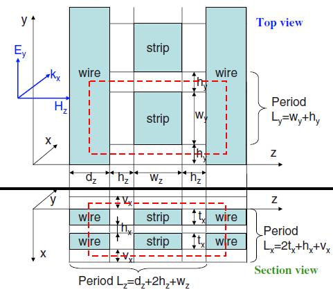
119 (e) (f) (g) (h) (i) (j) 114
 (n)")


120 (k) (l) (m) (n) (o) (p) 115
121 Figure 2: Examples of Metamaterial-based Absorbers (a,b) First experimental demonstration of a tunable absorber with simulated (solid) absorptivity and unit cell; (c,d) First absorber experimentally demonstrated in the THz regime and unit cell; (e,f) First absorber demonstrated in the millimeter wave regime and unit cell. (g,h) First absorber demonstrated to operate at wide angles. (i, j) First simulated prediction of a absorber in the IR frequency range and unit cell. (k, l) First experimental demonstration of a absorber in the MIR frequency range; (m, n) One of the first experimental demonstrations of absorber in the NIR range and unit cell. (o, p) Demonstration of absorber operating in the visible range and unit cell. Although the first experimental work on MPAs was in the microwave frequency regime, work quickly followed in the THz regime [12]. The design consisted of an ERR on top of a split wire separated by a polyimide spacer, shown in Figure 2c [12]. The absorption mechanism is nearly identical to the original experimental design in [11] with the ERR and split wire coupling strongly to the incident electric field and the magnetic field coupling to anti-parallel currents in the split wire and ERR. Simulations predicted an absorption of 98% at 1.12 THz and an experimental absorption of 70% at 1.3 THz was shown (Figure 2 d) [13]. A similar design was realized in the millimeter wave regime, utilizing slightly larger dimensions to achieve a resonance at approximately 80 GHz; the unit cell and the corresponding experimental results are shown in Figure 2e and 2f [14]. A down scaling of the geometry of the ERR and unit cell size enabled the first experimental demonstration of a metamaterial perfect absorber in the mid-infrared regime. An absorption of 97% at a wavelength of 6 μm was achieved (see Figure 2l) [15]. The unit cell design consists of a cross-shaped electric resonator above a ground plane separated by a dielectric layer. Unlike some of the original designs, a continuous ground plane that is thicker than the penetration depth of the light is used instead of a cut wire, thus preventing transmission while the ERR and ground plane combination provides the impedance matching necessary for zero reflectivity. In this case, the majority of the power loss occurs in the dielectric layer rather than by metallic ohmic loss in agreement with previous studies at lower frequencies [11]. 116
122 Earlier theoretical work predicted a plasmonic based near-infrared absorber based on a perfectly impedance matched negative index material and utilizing resonances in wires [16]. The unit cell design consists of coplanar layers, each of them having a cut wire surrounded by two continuous wires, all embedded in a dielectric, as shown in Figure 2i. Numerically, an absorption of A = 90% for a single layer is predicted in the IR region at 1.5 μ m (Figure 2j). However, even earlier theoretical and experimental work on a mid-infrared plasmonic based absorber was demonstrated [17]. The authors used a hexagonal array of circular metallic patches above a ground plane with a thin dielectric spacer. The reflectivity drops to approximately 17% at 5.8 μ m; the authors interpreted their results as due to plasmons trapped underneath the metallic patches. The first two works operating at NIR wavelengths [18,19] demonstrated absorption utilizing a structure similar to the aforementioned one [17]. Both studies utilized a unit cell which consisted of a gold disk or rectangle array over a gold ground plane separated by a dielectric spacer. The studies realized an absorption of 99% [19] and 88%, [18] both at roughly 1.6 μm wavelength as shown in Figure 2 m and n. The resonances, as reported also in [17] were described as plasmonic resonances between the gold nanoparticles and the gold plane; the absorption is due to local excitations of magnetic and electric dipole resonances [18]. The major loss component of the NIR absorbers was also investigated in [18] and shown to be Ohmic, in contrast to the absorbers operating at lower frequencies. The visible frequency regime represents a big deal for the electromagnetic community, especially for several fabrication issues [20]. Consequently, the experimental work done in this regime is not extensive as in the aforementioned ranges such as microwave, THz, or IR range. In spite of the particular operational frequency, there have been many efforts to test the limits of metamaterial-based absorbers by making them as efficient and effective as possible. One direction research in the optical frequency range is to make multi-band and broadband absorbers. 117


![Other ways of combining resonators in one unit cell can be realized; for example, by stacking multiple layers in which resonators share the same ground plane, [24] (see Figure 3b.](/docs-images/81/82819542/images/123-2.jpg "Another method utilizes the different sections of a single structure that resonate at different frequencies to obtain multiple resonances, [25] as shown in Figure 3c.")
123 One method utilizes multiple resonating structures in a single unit cell, exploiting the fact that resonators with different sizes resonate at different frequencies, as shown in Figure 3a. [21-23] By combining them in one unit cell, multiple resonances will rise in the absorption spectrum. If these resonances are close enough in frequency, then they will merge and form a broadband absorption. If they are further away from each other, then a multiple band absorber can be realized. Other ways of combining resonators in one unit cell can be realized; for example, by stacking multiple layers in which resonators share the same ground plane, [24] (see Figure 3b. Another method utilizes the different sections of a single structure that resonate at different frequencies to obtain multiple resonances, [25] as shown in Figure 3c. (a) (b) (c) Figure 3: (a) An absorber utilizing multiple elements. (b) Absorber that stacks multiple resonators on top of each other. (c) An absorber that uses different sections of the same resonator to achieve dual band absorption. 118
124 3. Other electromagnetic wave absorbers: plasmons, nanoparticles, subwavelength hole arrays, gratings The following paragraph outline several designs which absorb energy through different mechanisms than the more conventional metamaterial-based absorbers. Many of these absorbers have periodicities on the order of the wavelength, unlike traditional metamaterials which generally utilize subwavelength structures. In addition to this, many of these structures utilize resonances such as cavity or trapped modes to achieve high absorption. Plasmons It has been noted that the absorption mechanism for many metamaterial-based absorbers in the visible regime is due to near-field plasmon coupling between the top layer and the ground plane, the so-called localized surface plasmon resonance (LSPR). As reported before, this can have benefits for applications. For wide angles of incidence, the surface plasmon propagation length can become shorter than the lattice constant, and therefore make interactions between neighboring unit cells [26]. This has the potential application of making small absorbers for detection purposes. Nanoparticles Some absorber designs used conventional nanoparticles placed on top of or embedded in a dielectric layer above a ground plane. Many numerical studies were done on the use of nanoparticles for absorption, [27] specifically in their ability to achieve polarization insensitive and wide-angle absorptivity [28, 29] as well as a broadband or multi-band response. [27, 29, 30] The absorption mechanism is similar to cavity resonance modes. Subwavelength Hole Arrays Subwavelength hole arrays (SHAs) have been deeply studied for over a decade, mainly due to their use in enhanced transmission. [31] 119
125 One of the first numerical studies of a SHA based absorber operating in the NIR regime utilizes a simpler, one dimensional version of the SHA [32], revealing a suppression of trasmission and a simultaneous increase in absorption due to the surface plasmon resonances excitation in the structure. [33] Gratings A common design to achieve absorption in the NIR and visible regimes is the grating structure. There were many numerical studies done on the subject. [34-36] Among these were designs that are able to achieve: absorption at all incident polarizations, [34, 35] wide-angle operation, [34-36] and a broadband response. [35] The absorption mechanism is due to a combination of the surface plasmon resonance and the cavity resonance seen in waveguides. An experimental demonstration of a metal grating perfect absorber utilizes plasmonic nanowires and noted it s potential use as a sensor. [37] Non-Traditional metamaterial-based absorbers We have thoroughly investigated many metamaterial-based absorbers in the previous paragraph. In general, these absorbers have utilized a three-layer design with a ground plane or metallic structure supporting a dielectric and top metallic structure. However, there have been some metamaterial-based absorbers that have made alterations to this design or, in some cases, utilize metamaterials for absorption in an entirely different way, as it will be shown in the next paragraph. 4. Epsilon-Near-Zero electromagnetic wave absorbers From what we have seen so far, the major issues in the electromagnetic absorber design concern satisfying the following requirements: Small thickness: most of the presented absorbers require a thickness at least around λ/4 Broad angle range: the absorption is required at all angle of incidence 120
126 Broad bandwidth and multi-resonant behavior: wide the bandwidth of the single resonant frequency and/or create multiple resonant bands with the wider bandwidth possible Scaling the structure: the possibility to replicate the same behavior and performances in all the electromagnetic spectrum frequency ranges. The main goal, not easily achievable, is to satisfy all the features listed above at the same time. Recently, several studies focused their attention on a particular kind of metamaterials entitled epsilon-near-zero (ENZ) and on their particular electromagnetic properties. Such materials, characterized by low (mostly near zero) values of the real part of the relative permittivity, have several interesting applications such as tailoring the phase-front of an electromagnetic wave and designing filters [38], obtaining directive antennas [39], implementing optical nano-circuits [40], confining electromagnetic fields [41], enhancing transmission [42], obtaining anomalous tunneling effects [43, 44], focusing the electromagnetic field [45], cloaking objects [46, 47] improving sensing systems [48-50]. Recent evidence suggests that good absorption could be obtained by thin ENZs and MNZs with low loss [51] in thin anisotropic ENZ metamaterials [52] and with high losses MNZ materials [53]. Considering all these issues, in this paper, by exploiting the particular properties of ENZ materials we propose the design of an electromagnetic absorber. The purpose of this paragraph is to satisfy all the mentioned requirements at the same time. Thus the central objective is to obtain a good absorption level for different angles of incidence, at single and/or different resonant frequencies with the wider bandwidth possible, for small layer thicknesses. The paragraph is structured as follows: first of all, the general operation pattern is presented and analytically described by the use of the Transmission Line Theory. This provides us the possibility to correlate the electromagnetic properties of the structure (in terms of absorption magnitude and resonant frequency) with its geometrical characteristics. The proposed analytical model is compared to the results obtained by fullwave simulations. Then a description of the main important features of the ENZ absorber 121
 sheet.")
= ε 0 (ε r (ω)-jε i (ω)) and magnetic permeability μ ENZ =μ 0 μ r with μ r =1 the relative magnetic permeability of the free space")
127 is reported. Finally, a new geometrical solution, in order to improve the ENZ absorber properties, is proposed. 5. The ENZ absorber The structure under study is show in Figure 4a. An isotropic ENZ material slab with a thickness d is placed on top of an infinitely extended perfect electric conductor (PEC) sheet. The top layer and the ENZ slab are entitled as region 1 and region 2, respectively. Let s assume the region 1 as free space with electric permittivity ε 0 and magnetic permeability μ 0. The ENZ material is described by the electric permittivity ε ENZ (ω)= ε 0 (ε r (ω)-jε i (ω)) and magnetic permeability μ ENZ =μ 0 μ r with μ r =1 the relative magnetic permeability of the free space and ω=2πf is the frequency (rad/s). The structure is excited by an electromagnetic plane wave, having the electric field and the propagation vector k inclined to the ground plane with a generic Angle Of Incidence (AOI) α, as depicted in Figure 4(a). By using the Transmission Line Theory we developed an analytical approach to find the reflection coefficient r. The formula provides a powerful tool in order to link the absorption properties to the electromagnetic ENZ material ones (ε r and ε i ), the angle of incidence (α) and the thickness d of the ENZ layer. We consider each layer as a section of the transmission line, each of one characterized by their parameters, as depicted in Figure 4(b). In particular, Z=ηcos α is dependent on the angle of incidence α with η the free 0 space characteristic impedance (η=120π). Z ENZ is the impedance of the ENZ material, the PEC layer is represented by a short circuit. (a) (b) Figure 4: (a) A plane wave impinges (with an angle α) on an isotropic ENZ (thickness d) - PEC bilayer; (b) equivalent transmission line model. 122
128 Different ways in which electromagnetic energy can propagate at an interface, exist. Electromagnetic waves incident upon a boundary or surface may be reflected, transmitted, absorbed, scattered, or may excite surface electromagnetic waves. Let's consider wavelengths in the range of λ0, and assume that the surface has an average roughness that is much smaller than the characteristic wavelength, such that we may ignore scattering effects. The surface may also support plasmons or, more generally, surface electromagnetic waves. In addition we consider to have a flat surface such that any surface electromagnetic waves or plasmons extinguish before re-scattering. In this way we may then finally resolve that a wave may be reflected ( R ), transmitted ( T ), or absorbed ( A ), with their relationship given as A = 1 T R. In this case, due to the presence of the PEC, the transmission coefficient T is zero, so the corresponding absorption A is related to the reflection coefficient as A=1- r 2. As a consequence the absorption is obtained when the coefficient r approaches to 0. First of all we calculate the input impedance at the interface between air and the ENZ layer: ENZ α 2 η sin Z i= 1- Tanh dω ε ε ε Then, we calculate the reflection coefficient by using the relation: ENZ Z-Z = Z+Z 2 ENZ (1) i 0 r (2) i 0 where Z i is the total impedance of the ENZ and the PEC. In order to find a closed form formula the following simplification rules have been used [54]: 123
129 Cos Cosh Sin Sinh n k 1 n k 1 n k 1 1 n k k k k k The corresponding reflection coefficient formula reads: 2 2 (3) a ρ +a ρ +a ρ+a r = (4) b ρ +b ρ +b ρ+b being ρ=d/λ p (where λ p is the ENZ material plasma wavelength) and the coefficients: a = b = Cos [α] ε +ε r i 2 Tanh Sin [α]ε i 2 2 1/4 1 1 r i 2 2 ε i +εr εr-sin [α] a= -b= π Cos[α] ε +ε a 2= b 2=16-32πεrCos [α] ε r+εi ε a= -b= πarctan[ ]Cos[α] ε +ε i r i εr 3/4 For the normal incidence case, the formula simplify as follows: r= ε 3/4 i πarctan[ ] ε r +εi ρ +1-2εr ε r +εi ρ + ε r+εi εr ε 3/4 i πarctan[ ] ε r +εi ρ +1-2εr ε r +εi ρ + ε r+εi εr (5) Analytical results for the complete expression (without simplifications), the simplified one and the results obtained by full wave simulations are compared. Simulations are performed by using a frequency domain solver, implemented by the finite integration commercial code CST Microwave Studio [55]. In Figure 5 a comparison between analytical and numerical models for the reflection coefficient spectra as a function of AOI is presented. 124
130 The results, as shown in Figure 5, indicate that a good agreement among the results was achieved. (a) (b) (c) (d) Figure 5: Comparison of the reflection coefficient values, as a function of AOI, among the original analytical formula (without approximations), the proposed analytical formula (with approximations) and the numerical results for: (a) d/λ p =0.05, (b) d/λ p =0.1, (c) d/λ p =0.15, (d) d/λ p =0.2 (ε r =0.0015, ε i =0.5). 125
131 Electromagnetic absorption properties of Epsilon-Near-Zero Absorbers: comparison among Metamaterial Perfect Absorbers, Other Electromagnetic Wave Absorbers, and Epsilon-Near-Zero Absorbers As shown in equation (4) the reflection coefficient is a function (not simple) of the frequency, the angle of incidence α, the real/imaginary part of the ENZ material permittivity and the thickness d. By using the analytical models proposed, it is possible to study the effect of the geometrical (Angle Of Incidence (AOI) α and thickness d) and the electromagnetic parameters of the ENZ layer (electric permittivity in its real and imaginary part ε r and ε i, respectively) on the absorption characteristics of the structure. To describe the behavior of the structure under study with real materials, the dispersive permittivity models for Aluminum Zinc Oxide (AZO, f p =193THz), Gallium Zinc Oxide (GZO, f p =217THz) and Indium Tin Oxide (ITO, f p =210THz) Error! Reference source not found.56, 57] have been used. Effect of geometrical parameters We simulate the structure at different Angles Of Incidence (AOI), for the following thicknesses of the ENZ slab: d/λ p = 0.05, d/λ p = 0.1, d/λ p = 0.15, d/λ p = 0.2 and d/λ p = For example, Figure 6 shows the reflection coefficient r (color) plotted in a 2D domain of the AOI (degrees) and frequency (THz) for fixed thickness ratios d/λ p of GZO (Epsilon Near Zero region for 190THz f 260THz ). Similar results can be achieved by using other materials, such as AZO and ITO. It is apparent from this data set that, for small thicknesses (0.05 d/λ 0.1), the best absorption possible is reached only for very small angle range (50 α 70). By increasing the thickness (d/λ 0.2) two regions are present, in particular referring to Figure 6c, one (Region a) in the ENZ region and the other one (Region b) nearby it. For larger thicknesses (d/λ 0.25) the two regions are already present, but they collapse in one. As a consequence the absorption is obtained for a larger AOI range (0 α 60). Beyond the 80 the absorption is no longer significant. 126
 d/λ p =0.1, (c) d/λ p =0.2, (d) d/λ p =0.")

.")
132 (a) (b) (c) (d) Figure 6: Reflection coefficient as a function of AOI (degrees) and frequency (THz) of GZO (f p =217 THz) for: (a) d/λ p =0.05, (b) d/λ p =0.1, (c) d/λ p =0.2, (d) d/λ p =0.25 Effect of electromagnetic characteristics As mentioned above the reflection coefficient (consequently, the absorption) is also related to the ENZ electromagnetic characteristics. It is well known that the resonant frequency of the S11 parameter is related to the real part of the permittivity (ε r ) of the ENZ slab, instead the magnitude and the amplitude width of the S11 parameter is related to the imaginary part (ε i ). Keeping this in mind, in Figure 7 the reflection coefficient is reported as a function of the AOI for different values of the real part and imaginary part, for fixed values of the thickness, obtained by full wave simulations, and confirmed also by the analytical results. 127
133 (a) (b) Figure 7: Reflection coefficient as a function of AOI: (a) effect of the real part (with ε i =0.7), (b) effect of the imaginary part (with ε r =0.1). As noted from Figure 7 the real part does not affect too much the reflection coefficient magnitude and the angle range. On the other hand, the correlation between r and ε i is worth mentioning because, as expected, the reflection coefficient decreases when the ENZ losses grow. The absorption is relevant only for larger thicknesses, as also confirmed by equation (4). For normal incidence the reflection coefficient is at its minimum only when a large imaginary part of the ENZ material comes into play. Instead, for the AOI>0 the absorption is maximized if ε r is smaller than 2. Such results are consistent with previous results [53]. In addition to this, it was noted that: In the maximum absorption areas (as also shown in Figure 6) the real part is comparable (same magnitude order) to the imaginary one. In this case, the absorption is larger compared to the previous cases, as also confirmed by equations (4) and (5). The angle range, to which the greatest absorption is reached, is a function of the imaginary part (ε i ) 128
134 Figure 8: Reflection coefficient as a function of AOI for different thickness values (with ε r =0.4,ε i =0.5). The multi layered structure The angular reflections for different values of the thicknesses, namely, d/λ p =0.05, 0.1, 0.2 and 0.25 is shown in Figure 8. For normal incidence the reflection coefficient is reduced only when the thickness is large. This can be explained in the following way. From boundary conditions at the interface AIR ENZ we have the continuities of the tangential components E 1t =E 2t, instead the normal components are related in the following manner ε 1 E 1n = ε 2 E 2n across the separation surface. At the interface ENZ PEC we have the zero tangential component of the electric field condition on the PEC plate surface. As a consequence, the most interesting result, is that at normal incidence (α=0) the absorption can be exclusively attributed to the presence of both high losses and large thicknesses of the ENZ material (Figure 8). In this case the only component of the electric field is purely longitudinal and it doesn t affect the absorption. Instead, for all the other AOI α>0 a normal component of the electric field exists inside the ENZ layer. Such component is magnified by the ENZ layer. It s well known from boundary condition for the normal component that E = ε ε E 2n 1 2 1n, where ε 1=1 and ε 2 0. As a consequence, when the normal component of the electric field is present, to obtain a good absorption thin thicknesses can be used. 129

135 Research has tended to focus on designing highly lossy structures to reach the best absorption. This is not a big deal in the microwave range, where thin structures with a large imaginary part can be implemented easily. One of the major drawbacks considering infrared and/or optical frequencies is that materials have very low losses compared to the ones in the microwave range. This represents an important limitation in designing a good absorber: as a consequence in order to achieve a great absorption, a greater ENZ layer thickness is necessary. In the following an alternative solution, in order to overcome such a problem, is proposed. Our goal is to obtain absorption for different AOI and a wide resonant frequency band by using thin thicknesses. Let s consider a 3 layered structure: the two possible combinations are dielectric ENZ dielectric and vice versa (Figure 9). If the dielectric material (with high permittivity value) is the layer 1 (n 1 is really large) and the ENZ material is the layer 2 (n 2 0), we have (by applying the Snell s law at the interface dielectric ENZ): sin θ 2= n1 n2sinθ 1. As a consequence, for any angle of incidence (not zero), exists a normal component of the electric field in the ENZ layer, magnified as reported above, leading to a greater absorption. Figure 9: Multi layered structure proposed: Dielectric ENZ (thickness d) Dielectric. Results are reported in Figure 10a for the AZO material. Similar results can be obtained with the other two materials (GZO and AZO). Let us fix the good absorption criteria when the resonant tip reaches the value of 10dB. From Figure 10a it is possible to note how absorption is achieved at all angles, from 0 to 80 ; in particular at the same 130
136 frequency in the angle range 0 30 and for α>30 the central resonant frequency blue shifts and the bandwidth enlarges (40 70 ). (a) (b) Figure 10: Absorption of the proposed 3 layered structure: (a) multi frequency and wideband behavior (d tot /λ p =0.25); (b) multi band behavior (d tot /λ p =0.5, with d 1 /λ p =0.05, d 2 /λ p =0.2, d 3 /λ p =0.25, ε dielectric =100) It is interesting to note that if we release the lack of small thickness (the ratio d/ λ p = 0.25), by managing the different layers of the entire structure it is possible to reach absorption at different resonant frequencies in the ENZ region of the material. An example for multi band absorption is shown in Figure 10b. By using the proposed structure, for AOI in the range 0 50 two different absorption frequencies are present; instead for α>50 the absorption bandwidth enlarges significantly. The most remarkable point, from the achieved results, is that in this way we can obtain a good absorption: _ at all AOI in the range 0 80 : multi angle absorption _ at different resonant frequencies: multi frequency/multi band absorption _ a large frequency bandwidth: wideband absorption 131
137 6. Conclusions The potential role of ENZ materials to design a new electromagnetic absorber was investigated. Such a material, thanks to their peculiar properties, path new ways forward the design of electromagnetic absorbers, satisfying specific requirements. In this regard, first of all by using the Transmission Line Approach, a new analytical model, describing the electromagnetic absorption characteristics of the structure (in terms of magnitude, bandwidth and frequency position) is presented. The proposed model is compared to the results obtained by full-wave simulations. Good agreement among analytical and numerical results was obtained. By using both models the properties of the ENZ absorber were discussed. In addition to this, a new multi-layered structure was proposed in order to enhance the absorption. Full-wave simulations have confirmed the ability of the proposed configuration to behave as a multi-band and broadband absorber in a wide range of angle of incidence for small thicknesses. The proposed structure offers great potential in a wide variety of practical application fields such as to build-up selective thermal emitters, for detection and sensing, for imaging and defense applications. 7. Applications and future works Other than their rich ability as a platform to study fundamental electromagnetic wave theory, metamaterial-based absorber offer a wide variety of practical applications. Although many of these applications are still in their youth, a major goal since the creation of them has been to integrate them into existing devices to boost their performance. The following subparagraphs look at a few of the possible applications that are most studied in the field. 132
138 Military and Telecommunications applications Today, electromagnetic wave absorbers continue to have many relevant uses. One of the most widespread uses is for radar cross section (RCS) reduction. The basic goal of RCS reduction is to reduce radar echo so that objects can be hidden [4]. EM wave absorbers can also be used for antennas in reducing side lobe radiation or undesirable radiation from antennas [3]. Clearly, all of these applications have huge military and civilian potential. More recently, electromagnetic wave absorbers have been used in the reduction of electromagnetic interference by absorbing spurious electromagnetic radiation [3]. Along with preventing health risks due to exposure of specific electromagnetic radiation at particular frequencies, useful tool for wireless communications [58]. Detection and Sensing Because metamaterial-based absorbers are tunable with respect to their operational wavelength, they can be used as spectrally sensitive detectors or sensors. Much work has done in both integrating them into existing designs and creating novel devices based on metamaterials to provide detection and sensing throughout the electromagnetic spectrum. Microbolometers are a type of thermal detector in which incident electromagnetic radiation is absorbed by a material and then sensed by a thermometer. [59] In the pyroelectric detector, absorbed energy is sensed by a material that has a temperature dependent dielectric function, and the material forms a portion of a sensitive capacitive circuit. [60] These devices are of great interest in the IR wavelengths range and are particularly useful at THz frequencies. Theoretical work was done showing the possibility of adding a metamaterial-based absorber to conventional bolometer microbridges in the MIR region in order to introduce an element of spectral sensitivity. [61] In another example of metamaterial-based absorbers as detectors, in [62] it was able to show that SRR s could be implemented on cantilever pixels to detect light. Utilizing metamaterial-based absorbers to provide heat upon absorption (through their loss) can 133
139 cause mechanical displacement of the cantilever. By scaling the SRR design, this study was able to show photoresponsivity in the THz regime and in the microwave region. Rather than adding to an existing device, it is proposed that metamaterial-based absorbers themselves could act as plasmonic sensors in the NIR regime. [19] The idea behind a plasmonic sensor is that small changes of a material produce measurable changes in the optical properties of the sensor. In this case, the absorption characteristics would change, indicating change in the material surrounding the absorber: the relative intensity change is caused by a change in refractive index. Because change in refractive index of the surroundings causes a change in the impedance match conditions, a metamaterial-based absorber will act as a very sensitive plasmonic sensor. It was demostrated a FOM that is 4 times larger than plasmonic gold nanorod sensors. Other Applications There are a multitude of other applications for MPAs, only a few of which will be mentioned here. Certain regions of the millimeter wave realm have specific applications in technology. The millimeter wave bands studied in [63] are utilized in automotive radar (77 GHz), local area wireless network (92 95 GHz), and imaging (95 and 110 GHz). Additionally, absorbers in the millimeter range could be used for radar sensors for adaptive cruise control. [64] Metamaterial-based absorbers have been postulated to be useful for actively integrated photonic circuits, [65] spectroscopy and imaging, [66] and microwave-to-infrared signature control. [67] Future works In addition to applications discussed above, there are many great options for future development of metamaterial-based absorbers. One is the advent of tunable, or active, metamaterial absorbers, making itself that could be dynamically tuned by means of external stimuli [68]. One particular accessible application of tunable metamaterial-based absorber is in imaging. Some work has been done on THz imaging using compressive sensing. [69] 134
140 Another possibility, is the application of metamaterial-based absorbers as accurate, tunable and efficient thermal emitters over a specific frequency range to maximize efficiency. [70] There are a multitude of challenges in the future of metamaterial-based absorbers; one is overcoming fabrication issues, specifically in the visible regime, to make them as efficient as possible. Another challenge is to integrate them into practical devices. Despite the difficulties and challenges faced by metamaterial-based absorbers, they have a bright future with many potential applications which should have a significant impact on current science and technology. Since their initial development, metamaterial-based absorbers have proved to be not only useful for a multitude of applications but also as a platform to investigate classical electromagnetic wave theory. 135
141 Metamaterial-based nanoantennas While antennas are a key enabling technology for devices like phones and Televisions by using electromagnetic radiation in the radio-wave or microwave regime, their optical version is essentially inexistent in today s technology. However, recent researches in nano-optics and plasmonics generated a huge interest in optical antennas, and several studies are at the moment focused on how to transfer the well-established radiowave and microwave antenna concepts into the optical frequency regime. The absence of optical antennas in technological applications is associated with their small scale. Typical Antennas have characteristic dimensions of the order of the operative wavelength, this constrain leads for demanding fabrication accuracies of the order of nanometers. The advent of nanotechnology provides access to this length scale with the use of novel nanofabrication tools. Optical antenna structures is an emerging opportunity for novel optoelectronic devices. Recently the field of optics has significantly grown and researchers have been able to prove that the optical antenna concept can realize the bridge between nanoscale optical signals and far-field optical radiation, analogous to what a conventional antenna represents for microwave and RF frequencies. Introduction Today, we are used to refer to an electromagnetic transmitter or receiver as an antenna [71]. Guglielmo Marconi introduced the term antenna in the context of radio in 1895 while performing his first wireless transmission experiments. Various antenna geometries have been developed since and many books have been written on antenna theory. In 1983, IEEE defined the antenna as a means for radiating or receiving radio waves [72]. At radio-frequencies (RF), antennas are a well-established technology capable of transmitting electromagnetic signals that are confined within very sub-wavelength volumes to the far-field region. Over a century after Hertz s first attempts to radiate wireless signals through air, microwave antenna designers have derived a variety of powerful tools to develop complex wireless communication links. 136
142 While radio antennas were well-developed as solutions for communications problems, optical antennas were developed for imaging purposes. In analogy to its radiowave and microwave counterparts, we define the optical antenna as a device designed to efficiently convert free-propagating optical radiation to localized energy, and vice versa. First microscopic methods, in which the field scattered from a tiny particle could be used as a light source, were described in [73]. The particle would convert free-propagating optical radiation into a localized field that would interact with a sample surface. Thinking of the surface as a receiver, the particle can be viewed as an optical antenna. The development of dark-field microscopy, the invention of scanning tunneling microscopy and the discovery of surface enhanced Raman scattering (SERS) gave rise to many theoretical studies aimed at predicting the electromagnetic field enhancement near electromagnetic wave-irradiated metal particles [74]. Ten years later, irradiated metal tips were proposed as optical antenna probes for near-field microscopy and optical trapping [90, 9], and then several antenna geometries have been studied (rods, bowties, etc.). IR antenna fabrication has expanded considerably in the past few decades, in order to fabricate many types of IR detectors, bolometers, and nanophotonic devices [75, 76]. Recent progress in nanotechnology has allowed us to discover large emission enhancements and significant boosting of the electromagnetic fields near nanoparticles, theoretically predicted and experimentally observed in many configurations [77], paving the way to the new field of optical antennas [78]. This concept was started by simply analyzing nanoparticles whose shape may remember the one of RF antennas such as nanodipole, nanodimer and nanobowtie antennas). Considering this, the aim of this chapter is to design a new kind of antenna by exploiting the extraordinary properties of the ENZ electromagnetic properties. This chapter is organized as follows: first of all the RF, Microwave and Plasmonic antenna concepts are revisited and brought to the higher frequency (infrared and optics). Secondly, a brief overview of the general operation pattern of the following structure: ENZ+AIR and ENZ+PEC Antenna, is shown. Then, relevant differences between optical and conventional antenna operation are pointed out. A comparison with the traditional structures PEC Antenna is reported. This provides us the possibility to correlate their 137
143 properties with their geometrical and electromagnetic characteristics. Finally, conclusions and possible applications are drawn in the final paragraph. 1. Nanoantenna theory and design In this thrilling environment it is crucial to transfer some of the expertise and design tools of RF antenna design to optical frequencies, in order to tailor the coupling between confined optical sources and emitters using the traditional theory, modeling and design tools developed in the radio frequency range. Essentially, light and radio waves are governed by the same equations, and therefore similar phenomena are expected. Unfortunately, a direct translation of conventional antenna design rules to optical frequencies is not possible, due to the fact that material properties, physical operation and wave-matter interaction change significantly when the operating frequency gets higher (near-infrared and visible spectrum). In addition to this, the corresponding antenna dimensions become comparable to the components of materials. Therefore, it is important to discuss the most important differences between optical and conventional (RF) antenna operation. First of all, metals have really different electromagnetic response at optical frequencies compared to RF. Conventional RF antennas are usually realized with very good conductors characterized by highly sub-wavelength, usually negligible skin depth, in which conduction phenomena largely dominate. At optical frequencies, however, conductivity is generally lower and polarization and displacement effects play the crucial role. In this way, it modifies the physics of antenna operation, and the definition of currents and radiation properties of the antenna needs to consider displacement effects, in addition to the conduction ones. This is also usually manifested in the appearance of plasmonic effects, associated with field penetration in the metal. One aspect of this modification of the metal properties is reflected into the different propagation properties along a metallic rod at optical frequencies. If the conduction currents at RF have a wavelength equal to that of free-space, since no fields effectively penetrate into the metal, at optical frequencies the displacement currents flowing along the metal have much shorter wavelengths than free-space [79]. This leads 138
144 to an important consequence: the resonant length of a radio-frequency wire antenna is usually comparable to half-wavelength of operation, whereas it becomes significantly smaller for optical antennas [80, 81]. Related to the larger field penetration in metals, loss and absorption may also become relatively more important in optical antennas, affecting radiation efficiency and gain. In addition, these effects are associated with the manifestation of the aforementioned plasmonic effects at the interface of optical metals [82]. Finally, sources usually available at optical frequencies have significantly different properties than those available at RF. Depending on the quantum mechanisms describing their emission properties, and in particular their efficiency, the corresponding circuit model describing their emission and feeding properties may considerably change [83, 84]. 2. Nano-circuit theory for optical antennas At radio-frequencies, it is used to describe antenna systems by modeling their design in terms of few quantities of interest, such as its input impedance, bandwidth, directivity and gain. The power of this approach is fundamentally based on the fact that it is possible to describe transmitting and receiving antennas, as seen by the feeding or receiving lines, in terms of lumped circuit loads [85, 86]. The goal of this paragraph is to transfer traditional FR concepts to optical antennas and show that it is indeed possible to treat them in the same way. The concept is shown in Figure 11, in which it is shown an analogy between an optical nanodipole and a more conventional radio-frequency dipole, both of them fed at their gap. In order to properly show the equivalence, we need to bring into play the concept of optical nanocircuit impedance [87, 88]: a quantitative description of light interaction with small nanoparticles in terms of equivalent lumped circuit elements, in order to derive circuit theory tools for optical frequencies analogous to those available at lower frequencies to RF engineers. In this way, it is possible to define circuit quantities like (voltage) V and (displacement current) I d, and therefore the nanoantenna optical input impedance [89]. 139

145 Figure 11: (a) Optical nanodipole driven by an embedded optical source at its gap; (b) a plasmonic nanostrip line feeding a nanodipole antenna; (c) Thevenin equivalent circuit model for these transmitting optical antennas. Despite the same modeling approach, there are still huge differences between radiofrequency and optical impedances, currents and voltages. RF (conduction) currents are forced to be zero at the end of the antenna arms, whereas displacement currents are not necessarily zero at the edge of it. This makes the effective length of optical antennas usually longer than their physical length [90], with clear implications on their resonance frequency, which is usually shifted to longer wavelengths compared to RF antennas. Similar to RF antennas, input impedance is independent of the specific form of excitation but it depends on the choice of terminal points, as well as on the overall antenna shape and geometry, and it may be numerically calculated by applying an arbitrary voltage across the terminals and measuring the induced current flowing 140
146 across the gap. This implies that it is possible to fully describe the terminals of an optical antenna, both in transmitting and receiving operation, using the circuit model in Figure 11. A peculiar difference is that in determining the optical input impedance, the size and geometry of the antenna gap play a mainly important role compared to RF antennas. The gap forms a non-negligible nanocapacitance. This intrinsic load contributes to the overall input impedance in the circuit model (Figure 11), formed by the parallel combination of the gap impedance and the intrinsic impedance of the nanoantenna. This may represent an important advantage in working with optical antennas, because the load impedance may be easily modified by placing a specific material inside the antenna gap, providing interesting possibilities for tuning [91] and matching [92] the optical antenna. Using numerical simulations, the input impedance can be calculated by driving the antenna at the gap with an ideal impressed voltage source placed between the nanoantenna terminals and calculating the flux of displacement current flowing across the nanoantenna arms at the terminals. The ratio between the applied voltage and this current flux defines Z in. The general behavior of the dispersion of the optical input impedance is similar to that of a conventional RF antenna. There are few relevant differences typical of optical antennas, which are important to emphasize: First of all, the position of the resonant frequency, strictly related to the different propagation properties of the guided modes along the structure, affected by the non-negligible field penetration in the metal. The amplitude of the peak values of input resistance and reactance at the opencircuit resonances, which are much larger than in conventional RF antennas. Similarly, the input resistance at the short-circuit resonances is significantly lower than those of RF dipoles. This is associated with the smaller radiation resistance of optical antennas [93], due to the fact that their resonant lengths are much smaller than those at RF frequencies. 141
147 The input impedance obviously is not the only quantity of interest to characterize the radiation properties of optical antennas. As reported in [93], the optical radiation resistance in the visible, is usually smaller than at RF, due to the shorter resonant length and when it is combined with the larger metal losses, which increases the importance of the absorption resistance seen at the gap, lower radiation efficiencies generally are obtain compared to RF, due to the lower level of metal conductivity at these high frequencies. Directivity and gain may be defined similar to RF, and the main difference compared to conventional antennas is that they tend to be smaller, due to the naturally small resonant size and efficiency, as detailed above. Directivities closer to 1.5 (traditional RF dipole) are commonly obtained. The bandwidth of optical antennas is usually small, due to their inherently small electrical size and the influence of material dispersion and plasmonic effects. Finally, there are evident differences in the optical propagation properties as compared to RF, and optical links are necessarily expected to operate in line-ofsight. 3. Epsilon-Near-Zero Antennas: Dielectric + ENZ cover and PEC + ENZ cover The operation pattern Figure 12 shows the structures under study: the ENZ+AIR antenna (a) is characterized by a cylindrical air dipole with radius a=αλ p, length l=βλ p, embedded in a concentric ENZ material cylinder as cover, whose thickness is s=γλ p, where λ p is the plasma frequency of the ENZ material. The ENZ permittivity is described by the complex electric permittivity ε ENZ (ω)= ε 0 (ε r (ω)-jε i (ω)) and magnetic permeability μ ENZ = μ 0 μ r (being μ r =1 the relative magnetic permeability of the free space and ω=2πf is the frequency in rad/s). The antenna system is excited by a discrete port placed between two circular metallic plates in the middle of the dipole. The metallic plates are filled by the ENZ material too, whose thickness is d=δλ p. Let s assume the surrounding region as free space with electric permittivity ε 0 and magnetic permeability μ
148 senz = γλp Air (εr=1) ENZ layer εenz=εr-jεi lair/pec= βλp Air/PEC lenz= lair/pec + 2 γλp λp plasma wavelength rair= αλp renz= rair + γλp Figure 12: The antenna system operation pattern for: the ENZ+AIR antenna and the PEC+ENZ antenna. Comparison among ENZ Antennas and Classical Metallic Antennas In order to compare the traditional PEC electromagnetic behavior with the proposed ENZ structures, the following relevant major differences/aspects between ENZ-based and traditional antennas must be pointed out. First of all the different electromagnetic response of metals: it s well know that at RF and microwave frequencies antennas are realized with very conductors elements, in which skin depth can be neglected and the conduction phenomena largely dominate. Metallic wires function as conduits for the flow of electronic charges and the relative conduction currents. Metals due to their high conductivity σ, when surrounded by insulators (having zero or low conductivity) as free space, play the role of a medium with high contrast in electric conductivity, leading to the confinement of the conduction currents σe [94-96]. However, at higher frequencies (infrared and optical ones) the conductivity is lower and the polarization/displacement effects grow, becoming more relevant especially when the wavelength is reduced. At higher frequencies electric displacement currents play a more dominant role than the conduction ones. It means that at such frequencies the conduction current has to be substituted with the displacement one: -jωεe where E is the electric field and ε is the local material permittivity [97-98]. 143
149 Unlike the conduction current, in this case the displacement one can flow in the surrounding background material. Therefore in order to confine the displacement current, in the same way as metallic wires confine the conduction one, we have to replicate the contrast in conductivity existing between the metallic wire and the surrounding space. In other words the role of material conductivity is replaced by the material permittivity. The equivalent of a poor conductive material is represented by the epsilon near zero (ENZ) material in which, due to its low (nearly zero, ε<<1) permittivity values, the displacement current is close to zero. In this way the ENZ material play as an insulator for the displacement current, exactly the same role that air (very poorly conducting material σ 0) plays for the conduction current. Analogously, the role of the metallic wire in classical antennas (good conductor σ>>1) may be taken here by a dielectric with high permittivity values (ε 1). In this way the large contrast in the permittivity values is reached and the displacement current can flow in the dielectric medium as the conduction current flows on metals. Secondly, in traditional antennas no fields penetrate into the metal due to the large wavelength (comparable in terms of order of magnitude to that of free space) leading to a small penetration depth effect. On the other hand, at optical frequencies the wavelength is dramatically reduced, as a consequence the skin depth cannot be neglected anymore. Such differences, existing for metals at optical frequencies, are still valid in our case, leading to crucial consequences: the definition of voltage and current (and consequently the impendence concept) change. In particular we have to refer to the integral quantities of the local field distribution and the related displacement field around and inside the structure, as reported in [99] if in traditional radio-frequency the physical and resonant length of a wire antenna are comparable (half-wavelength of operation), at higher frequencies the guided wavelength on the arms of the optical antenna becomes significantly smaller than in free space [83, 84]. On the other hand, conduction currents are forced to be zero at the end of the antenna arms, at the optical regime the displacement current is not necessarily zero at the edge of the antenna. So the effective antenna length 144
150 results longer compared to its physical one, and the related resonant frequency is shifted to higher wavelengths compared to the traditional case. due to the larger penetration of the field, loss and absorption become more important in optical antennas, affecting their radiation efficiency and gain. We started to study a planar small circular capacitor (radius a and thickness d) filled with ENZ material and we compared it s behavior with a traditional air-filled capacitor. When the ratios radius to plasma wavelength and thickness to plasma wavelength, respectively are small, compared to the air-filled case: in the ENZ capacitor most of all the electric field lines are outside the gap: due to the low permittivity value of the ENZ material inside the capacitor, and follow the geometry of the structure the ENZ capacitor radiates an electromagnetic field, that it is more intense in proximity of the structure: due to the presence of the ENZ in the capacitance the electric field lines are forced to escape from the ENZ material and find a way (the air in this case) where propagate themselves. The intensification of the field outside the structure is larger if both the real and imaginary part of the ENZ material are kept small We simulated the electromagnetic field distribution of the considered structures by using the commercial electromagnetic software CST Microwave Studio [55]. 145
 and conduction current (b) distribution for the AIR+ENZ and PEC+ENZ antenna,")
151 (a) (b) Figure 13: Vector field plot (the real part) of (a) the displacement electric field and (b) the conduction current distribution for the AIR+ENZ and PEC+ENZ antenna, respectively. The results are shown in Figure 13, where the vector plot is the real part of the displacement electric field (a) and conduction current (b) distribution for the AIR+ENZ and PEC+ENZ antenna, respectively. 146
SCATTERING CROSS SECTION OF A META-SPHERE
 Progress In Electromagnetics Research Letters, Vol. 9, 85 91, 009 SCATTERING CROSS SECTION OF A META-SPHERE A. Alexopoulos Electronic Warfare and Radar Division Defence Science and Technology Organisation
Enhancing and suppressing radiation with some permeability-near-zero structures
 Enhancing and suppressing radiation with some permeability-near-zero structures Yi Jin 1,2 and Sailing He 1,2,3,* 1 Centre for Optical and Electromagnetic Research, State Key Laboratory of Modern Optical
Plasmonic metamaterial cloaking at optical frequencies
 Plasmonic metamaterial cloaking at optical frequencies F. Bilotti *, S. Tricarico, and L. Vegni Department of Applied Electronics, University Roma Tre Via della Vasca Navale 84, Rome 146, ITALY * Corresponding
GENERALIZED SURFACE PLASMON RESONANCE SENSORS USING METAMATERIALS AND NEGATIVE INDEX MATERIALS
 Progress In Electromagnetics Research, PIER 5, 39 5, 005 GENERALIZED SURFACE PLASMON RESONANCE SENSORS USING METAMATERIALS AND NEGATIVE INDEX MATERIALS A. Ishimaru, S. Jaruwatanadilok, and Y. Kuga Box
Workshop on New Materials for Renewable Energy
 2286-6 Workshop on New Materials for Renewable Energy 31 October - 11 November 201 Metamaterials: Past, Present, and Future Nonlinear Physics Centre Research School of Physics and Engineering The Australian
Road Map. Potential Applications of Antennas with Metamaterial Loading
 Road Map Potential Applications of Antennas with Metamaterial Loading Filiberto Bilotti Department of Applied Electronics University of Roma Tre Rome, Italy The history of metamaterials Metamaterial terminology
Robustness in design and background variations in metamaterial/plasmonic cloaking
 RADIO SCIENCE, VOL. 43,, doi:10.1029/2007rs003815, 2008 Robustness in design and background variations in metamaterial/plasmonic cloaking Andrea Alù 1 and Nader Engheta 1 Received 17 December 2007; revised
07/7001 METAMATERIALS FOR SPACE APPLICATIONS
 07/7001 METAMATERIALS FOR SPACE APPLICATIONS Type of activity: Medium Study (4 months, 25 KEUR) Background and Motivation Brief description of the Metamaterial concept Metamaterials could be considered
Analysis of Metamaterial Cloaks Using Circular Split Ring Resonator Structures
 Copyright 216 Tech Science Press CMC, Vol.53, No.3, pp.132-14, 216 Analysis of Metamaterial Cloaks Using Circular Split Ring Resonator Structures Susan Thomas 1 and Dr. Balamati Choudhury 2 Abstract A
Cloaking The Road to Realization
 Cloaking The Road to Realization by Reuven Shavit Electrical and Computer Engineering Department Ben-Gurion University of the Negev 1 Outline Introduction Transformation Optics Laplace s Equation- Transformation
Super-reflection and Cloaking Based on Zero Index Metamaterial
 Super-reflection and Cloaking Based on Zero Index Metamaterial Jiaming Hao, Wei Yan, and Min Qiu Photonics and Microwave ngineering, Royal Institute of Technology (KTH), lectrum 9, 164 4, Kista, Sweden
ANALYTICAL MODEL OF A METASURFACE CONSIST- ING OF A REGULAR ARRAY OF SUB-WAVELENGTH CIRCULAR HOLES IN A METAL SHEET
 Progress In Electromagnetics Research M, Vol. 18, 209 219, 2011 ANALYTICAL MODEL OF A METASURFACE CONSIST- ING OF A REGULAR ARRAY OF SUB-WAVELENGTH CIRCULAR HOLES IN A METAL SHEET D. Ramaccia *, F. Bilotti,
Evanescent modes stored in cavity resonators with backward-wave slabs
 arxiv:cond-mat/0212392v1 17 Dec 2002 Evanescent modes stored in cavity resonators with backward-wave slabs S.A. Tretyakov, S.I. Maslovski, I.S. Nefedov, M.K. Kärkkäinen Radio Laboratory, Helsinki University
Wavelength Dependent Microwave Devices Based on Metamaterial Technology. Professor Bal Virdee BSc(Eng) PhD CEng FIET
 PhD CEng FIET") Wavelength Dependent Microwave Devices Based on Metamaterial Technology by Professor Bal Virdee BSc(Eng) PhD CEng FIET EM response of materials are determined by the spatial distribution of its atoms and
Wavelength Dependent Microwave Devices Based on Metamaterial Technology by Professor Bal Virdee BSc(Eng) PhD CEng FIET EM response of materials are determined by the spatial distribution of its atoms and
EPSILON-NEAR-ZERO (ENZ) AND MU-NEAR-ZERO (MNZ) MATERIALS
 AND MU-NEAR-ZERO (MNZ) MATERIALS") EPSILON-NEAR-ZERO (ENZ) AND MU-NEAR-ZERO (MNZ) MATERIALS SARAH NAHAR CHOWDHURY PURDUE UNIVERSITY 1 Basics Design ENZ Materials Lumped circuit elements Basics Decoupling Direction emission Tunneling Basics
EPSILON-NEAR-ZERO (ENZ) AND MU-NEAR-ZERO (MNZ) MATERIALS SARAH NAHAR CHOWDHURY PURDUE UNIVERSITY 1 Basics Design ENZ Materials Lumped circuit elements Basics Decoupling Direction emission Tunneling Basics
Flute-Model Acoustic Metamaterials with Simultaneously. Negative Bulk Modulus and Mass Density
 Flute-Model Acoustic Metamaterials with Simultaneously Negative Bulk Modulus and Mass Density H. C. Zeng, C. R. Luo, H. J. Chen, S. L. Zhai and X. P. Zhao * Smart Materials Laboratory, Department of Applied
A Broadband Flexible Metamaterial Absorber Based on Double Resonance
 Progress In Electromagnetics Research Letters, Vol. 46, 73 78, 2014 A Broadband Flexible Metamaterial Absorber Based on Double Resonance ong-min Lee* Abstract We present a broadband microwave metamaterial
Electromagnetic Absorption by Metamaterial Grating System
 PIERS ONLINE, VOL. 4, NO. 1, 2008 91 Electromagnetic Absorption by Metamaterial Grating System Xiaobing Cai and Gengkai Hu School of Science, Beijing Institute of Technology, Beijing 100081, China Abstract
Optical Properties of Left-Handed Materials by Nathaniel Ferraro 01
 Optical Properties of Left-Handed Materials by Nathaniel Ferraro 1 Abstract Recently materials with the unusual property of having a simultaneously negative permeability and permittivity have been tested
Pairing an Epsilon-Negative Slab With a Mu- Negative Slab: Resonance, Tunneling and Transparency
 University of Pennsylvania ScholarlyCommons Departmental Papers (ESE) Department of Electrical & Systems Engineering 10-1-2003 Pairing an Epsilon-Negative Slab With a Mu- Negative Slab: Resonance, Tunneling
Nonlinear Metamaterial Composite Structure with Tunable Tunneling Frequency
 Progress In Electromagnetics Research Letters, Vol. 71, 91 96, 2017 Nonlinear Metamaterial Composite Structure with Tunable Tunneling Frequency Tuanhui Feng *,HongpeiHan,LiminWang,andFeiYang Abstract A
Anomalies of Sub-Diffractive Guided-Wave Propagation along Metamaterial Nanocomponents
 University of Pennsylvania ScholarlyCommons Departmental Papers (ESE) Department of Electrical & Systems Engineering November Anomalies of Sub-Diffractive Guided-Wave Propagation along Metamaterial Nanocomponents
Magnetic response of split-ring resonator metamaterials: From effective medium dispersion to photonic band gaps
 PRAMANA c Indian Academy of Sciences Vol. 78, No. 3 journal of March 2012 physics pp. 483 492 Magnetic response of split-ring resonator metamaterials: From effective medium dispersion to photonic band
Extinction properties of a sphere with negative permittivity and permeability
 PERGAMON Solid State Communications 116 (2000) 411 415 www.elsevier.com/locate/ssc Extinction properties of a sphere with negative permittivity and permeability R. Ruppin* Department of Physics and Applied
Finite-difference time-domain analysis of the tunneling and growing exponential in a pair of ε- negative and µ-negative slabs
 University of Pennsylvania ScholarlyCommons Departmental Papers (ESE) Department of Electrical & Systems Engineering 7-18-2006 Finite-difference time-domain analysis of the tunneling and growing exponential
Frequency Dependence Effective Refractive Index of Meta Materials by Effective Medium Theory
 Advance in Electronic and Electric Engineering. ISSN 31-197, Volume 3, Number (13), pp. 179-184 Research India Publications http://www.ripublication.com/aeee.htm Frequency Dependence Effective Refractive
 Johnson, N.P. and Khokhar, A.Z. and Chong, H.M.H. and De La Rue, R.M. and McMeekin, S. (2006) Characterisation at infrared wavelengths of metamaterials formed by thin-film metallic split-ring resonator
New Aspects of Old Equations: Metamaterials and Beyond (Part 2) 신종화 KAIST 물리학과
 신종화 KAIST 물리학과") New Aspects of Old Equations: Metamaterials and Beyond (Part 2) 신종화 KAIST 물리학과 Metamaterial Near field Configuration in Periodic Structures New Material Material and Metamaterial Material Metamaterial
New Aspects of Old Equations: Metamaterials and Beyond (Part 2) 신종화 KAIST 물리학과 Metamaterial Near field Configuration in Periodic Structures New Material Material and Metamaterial Material Metamaterial
Left-handed and right-handed metamaterials composed of split ring resonators and strip wires
 Left-handed and right-handed metamaterials composed of split ring resonators and strip wires J. F. Woodley, M. S. Wheeler, and M. Mojahedi Electromagnetics Group, Edward S. Rogers Sr. Department of Electrical
Overview. 1. What range of ε eff, µ eff parameter space is accessible to simple metamaterial geometries? ``
 MURI-Transformational Electromagnetics Innovative use of Metamaterials in Confining, Controlling, and Radiating Intense Microwave Pulses University of New Mexico August 21, 2012 Engineering Dispersive
Optical Nanotransmission Lines: Synthesis of Planar Left-Handed Metamaterials in the Infrared and Visible Regimes
 University of Pennsylvania ScholarlyCommons Departmental Papers (ESE) Department of Electrical & Systems Engineering March 26 Optical Nanotransmission Lines: Synthesis of Planar Left-Handed Metamaterials
A Novel Design of Photonic Crystal Lens Based on Negative Refractive Index
 PIERS ONLINE, VOL. 4, NO. 2, 2008 296 A Novel Design of Photonic Crystal Lens Based on Negative Refractive Index S. Haxha 1 and F. AbdelMalek 2 1 Photonics Group, Department of Electronics, University
Design of Metamaterials in HFSS and Extraction of Permittivity and Permeability using NRW Method
 Design of Metamaterials in HFSS and Extraction of Permittivity and Permeability using NRW Method Monika Dhillon, Master of Technology student of Electronics and Communication Engineering of YMCA University
Nanoscale optical circuits: controlling light using localized surface plasmon resonances
 Nanoscale optical circuits: controlling light using localized surface plasmon resonances T. J. Davis, D. E. Gómez and K. C. Vernon CSIRO Materials Science and Engineering Localized surface plasmon (LSP)
APPLICATIONS ABSTRACT. The Electromagnetic metamaterials are defined as macroscopic composites, which are articially structured
 Proceeding of NCRIET-2015 & Indian J.Sci.Res. 12(1):261-266, 2015 ISSN: 0976-2876 (Print) ISSN: 2250-0138 (Online) OVERVIEW ON METAMATERIAL PHYSIC AND ENGINEERING APPLICATIONS DHERE VIDYASHREE V. a1 AND
New Concept Conformal Antennas Utilizing Metamaterial and Transformation Optics
 New Concept Conformal Antennas Utilizing Metamaterial and Transformation Optics The MIT Faculty has made this article openly available. Please share how this access benefits you. Your story matters. Citation
Canalization of Sub-wavelength Images by Electromagnetic Crystals
 Progress In Electromagnetics Research Symposium 2005, Hangzhou, China, August 22-26 37 Canalization of Sub-wavelength Images by Electromagnetic Crystals P. A. Belov 1 and C. R. Simovski 2 1 Queen Mary
RECIPROCAL INVISIBLE CLOAK WITH HOMOGE- NEOUS METAMATERIALS
 Progress In Electromagnetics Research M, Vol. 21, 15 115, 211 RECIPROCAL INVISIBLE CLOAK WITH HOMOGE- NEOUS METAMATERIALS J. J. Yang, M. Huang *, Y. L. Li, T. H. Li, and J. Sun School of Information Science
TUNABLE METAMATERIAL DESIGN COMPOSED OF TRIANGULAR SPLIT RING RESONATOR AND WIRE STRIP FOR S- AND C- MICROWAVE BANDS
 Progress In Electromagnetics Research B, Vol. 22, 341 357, 2010 TUNABLE METAMATERIAL DESIGN COMPOSED OF TRIANGULAR SPLIT RING RESONATOR AND WIRE STRIP FOR S- AND C- MICROWAVE BANDS C. Sabah Johann Wolfgang
Negative epsilon medium based optical fiber for transmission around UV and visible region
 I J C T A, 9(8), 2016, pp. 3581-3587 International Science Press Negative epsilon medium based optical fiber for transmission around UV and visible region R. Yamuna Devi*, D. Shanmuga Sundar** and A. Sivanantha
Alternative approaches to electromagnetic cloaking and invisibility
 Helsinki University of Technology SMARAD Centre of Excellence Radio Laboratory Alternative approaches to electromagnetic cloaking and invisibility Sergei Tretyakov and colleagues December 2007 What is
Suprabhat Vishwakarma 1, Bimal garg 2 1 Student, 2 Associate Professor. Electronics Department, Mitsgwalior (m.p.) India.
 India.") A L-Band Rectangular Shape Inside a Pentagon Metamaterial Structure for Microwave Application Suprabhat Vishwakarma 1, Bimal garg 2 1 Student, 2 Associate Professor Electronics Department, Mitsgwalior
A L-Band Rectangular Shape Inside a Pentagon Metamaterial Structure for Microwave Application Suprabhat Vishwakarma 1, Bimal garg 2 1 Student, 2 Associate Professor Electronics Department, Mitsgwalior
Constitutive parameter extraction and experimental validation of single and double negative metamaterials Y. Hollander 1 R.
 Published in IET Microwaves, Antennas & Propagation Received on 20th January 2010 Revised on 27th May 2010 ISSN 1751-8725 Constitutive parameter extraction and experimental validation of single and double
APPLICATION OF BILAYER ANISOTROPIC STRUC- TURES FOR DESIGNING LOW-PASS FILTERS AND PO- LARIZERS
 Progress In Electromagnetics Research M, Vol. 29, 95 108, 2013 APPLICATION OF BILAYER ANISOTROPIC STRUC- TURES FOR DESIGNING LOW-PASS FILTERS AND PO- LARIZERS Amir Raeesi *, Ali Abdolali, and Hossein Mirzaei
Chapter 5. Photonic Crystals, Plasmonics, and Metamaterials
 Chapter 5. Photonic Crystals, Plasmonics, and Metamaterials Reading: Saleh and Teich Chapter 7 Novotny and Hecht Chapter 11 and 12 1. Photonic Crystals Periodic photonic structures 1D 2D 3D Period a ~
Progress In Electromagnetics Research, PIER 35, , 2002
 Progress In Electromagnetics Research, PIER 35, 315 334, 2002 NUMERICAL STUDIES OF LEFT HANDED METAMATERIALS C. D. Moss, T. M. Grzegorczyk, Y. Zhang, and J. A. Kong Research Laboratory of Electronics Massachusetts
Bandwidth Enhancement of RMPA Using 2 Segment Labyrinth Metamaterial at THz
 Materials Sciences and Applications, 2013, 4, 579-588 http://dx.doi.org/10.4236/msa.2013.410071 Published Online October 2013 (http://www.scirp.org/journal/msa) 579 Bandwidth Enhancement of RMPA Using
Design of invisibility cloaks for reduced observability of objects
 ESTEC 13 June 2008 Design of invisibility cloaks for reduced observability of objects F. Bilotti, S. Tricarico, and L. Vegni University ROMA TRE, Italy Department of Applied Electronics Applied Electromagnetics
THE PROPAGATION AND CUTOFF FREQUENCIES OF THE RECTANGULAR METALLIC WAVEGUIDE PAR- TIALLY FILLED WITH METAMATERIAL MULTILAYER SLABS
 Progress In Electromagnetics Research M, Vol. 9, 35 40, 2009 THE PROPAGATION AND CUTOFF FREQUENCIES OF THE RECTANGULAR METALLIC WAVEGUIDE PAR- TIALLY FILLED WITH METAMATERIAL MULTILAYER SLABS D. Zhang
THEORETICAL EXAMINATION OF ELECTROMAG- NETIC WAVE TUNNELING THROUGH CASCADED ɛ-
 Progress In Electromagnetics Research B, Vol. 4, 1, 01 THEORETICAL EXAMINATION OF ELECTROMAG- NETIC WAVE TUNNELING THROUGH CASCADED ɛ- AND µ-negative METAMATERIAL SLABS C. H. Liu * and N. Behdad Department
Author(s) Tamayama, Y; Nakanishi, T; Sugiyama. Citation PHYSICAL REVIEW B (2006), 73(19)
 Tamayama, Y; Nakanishi, T; Sugiyama. Citation PHYSICAL REVIEW B (2006), 73(19)") Observation of Brewster's effect fo Titleelectromagnetic waves in metamateri theory Author(s) Tamayama, Y; Nakanishi, T; Sugiyama Citation PHYSICAL REVIEW B (2006), 73(19) Issue Date 2006-05 URL http://hdl.handle.net/2433/39884
Observation of Brewster's effect fo Titleelectromagnetic waves in metamateri theory Author(s) Tamayama, Y; Nakanishi, T; Sugiyama Citation PHYSICAL REVIEW B (2006), 73(19) Issue Date 2006-05 URL http://hdl.handle.net/2433/39884
Improvement in Characteristics of Micro strip Antenna with the Help of Different Meta material Structures
 IJIRST International Journal for Innovative Research in Science & Technology Volume 1 Issue 6 November 2014 ISSN (online): 2349-6010 Improvement in Characteristics of Micro strip Antenna with the Help
Light Localization in Left-Handed Media
 Vol. 112 (2007) ACTA PHYSICA POLONICA A No. 4 Proceedings of the 3rd Workshop on Quantum Chaos and Localisation Phenomena Warsaw, Poland, May 25 27, 2007 Light Localization in Left-Handed Media M. Rusek,
Effects of Loss Factor on Plane Wave Propagation through a Left-Handed Material Slab
 Vol. 113 (2008) ACTA PHYSICA POLONICA A No. 6 Effects of Loss Factor on Plane Wave Propagation through a Left-Handed Material Slab C. Sabah Electrical and Electronics Engineering Department, University
FDTD Analysis on Optical Confinement Structure with Electromagnetic Metamaterial
 Memoirs of the Faculty of Engineering, Okayama University, Vol. 44, pp. 1-6, January 21 FDTD Analysis on Optical Confinement Structure with Electromagnetic Metamaterial Shinji NAGAI, Ryosuke UMEDA, Kenji
A NEW ACCURATE MODEL OF HIGH-IMPEDANCE SURFACES CONSISTING OF CIRCULAR PATCHES
 Progress In Electromagnetics Research M, Vol. 21, 1 17, 211 A NEW ACCURATE MODEL OF HIGH-IMPEDANCE SURFACES CONSISTING OF CIRCULAR PATCHES D. Ramaccia *, A. Toscano, and F. Bilotti Department of Applied
WAVEGUIDES FILLED WITH BILAYERS OF DOUBLE- NEGATIVE (DNG) AND DOUBLE-POSITIVE (DPS) METAMATERIALS
 AND DOUBLE-POSITIVE (DPS) METAMATERIALS") Progress In Electromagnetics Research B, Vol., 75 9, WAVEGUIDES FILLED WITH BILAYERS OF DOUBLE- NEGATIVE (DNG) AND DOUBLE-POSITIVE (DPS) METAMATERIALS E. Cojocaru * Department of Theoretical Physics, Horia
Progress In Electromagnetics Research B, Vol., 75 9, WAVEGUIDES FILLED WITH BILAYERS OF DOUBLE- NEGATIVE (DNG) AND DOUBLE-POSITIVE (DPS) METAMATERIALS E. Cojocaru * Department of Theoretical Physics, Horia
The Dielectric Function of a Metal ( Jellium )
") The Dielectric Function of a Metal ( Jellium ) Total reflection Plasma frequency p (10 15 Hz range) Why are Metals Shiny? An electric field cannot exist inside a metal, because metal electrons follow the
The Dielectric Function of a Metal ( Jellium ) Total reflection Plasma frequency p (10 15 Hz range) Why are Metals Shiny? An electric field cannot exist inside a metal, because metal electrons follow the
Electromagnetic wave propagation through ultra-narrow channels filled
 31st October, HKUST, Hong-Kong Electromagnetic wave propagation through ultra-narrow channels filled with an ENZ material Mário G. Silveirinha How to have ε-nearε zero (ENZ) Media? 2 ω p ε r ~1 ω ω ( +
GHz magnetic response of split ring resonators
 Photonics and Nanostructures Fundamentals and Applications 2 (2004) 155 159 www.elsevier.com/locate/photonics GHz magnetic response of split ring resonators Lei Zhang a, G. Tuttle a, C.M. Soukoulis b,
Left-handed materials: Transfer matrix method studies
 Left-handed materials: Transfer matrix method studies Peter Markos and C. M. Soukoulis Outline of Talk What are Metamaterials? An Example: Left-handed Materials Results of the transfer matrix method Negative
CHAPTER 9 ELECTROMAGNETIC WAVES
 CHAPTER 9 ELECTROMAGNETIC WAVES Outlines 1. Waves in one dimension 2. Electromagnetic Waves in Vacuum 3. Electromagnetic waves in Matter 4. Absorption and Dispersion 5. Guided Waves 2 Skip 9.1.1 and 9.1.2
ARTIFICIAL DIELECTRIC SUBSTRATE FOR MICROWAVE APPLICATIONS
 ARTIFICIAL DIELECTRIC SUBSTRATE FOR MICROWAVE APPLICATIONS DOC. ING. JAN MACHÁČ, DRSC. PROF. ING. JÁN ZEHENTNER, DRSC. Abstract: This paper presents a new version of an artificial dielectric substrate.
Progress In Electromagnetics Research, PIER 97, , 2009
 Progress In Electromagnetics Research, PIER 97, 407 416, 2009 PRACTICAL LIMITATIONS OF AN INVISIBILITY CLOAK B. L. Zhang Research Laboratory of Electronics Massachusetts Institute of Technology MA 02139,
An Electrically Engineered Meta-Material Absorber
 An Electrically Engineered Meta-Material Absorber Shi (Mark) Gu Advised By: Dr. Steven Cummer Submitted in Partial Fulfillment of Graduation with Distinction Requirements On: 4-20-2009 1 Abstract Recent
Gradient-index metamaterials and spoof surface plasmonic waveguide
 Gradient-index metamaterials and spoof surface plasmonic waveguide Hui Feng Ma State Key Laboratory of Millimeter Waves Southeast University, Nanjing 210096, China City University of Hong Kong, 11 October
PHYSICAL REVIEW B 71,
 Coupling of electromagnetic waves and superlattice vibrations in a piezomagnetic superlattice: Creation of a polariton through the piezomagnetic effect H. Liu, S. N. Zhu, Z. G. Dong, Y. Y. Zhu, Y. F. Chen,
3D PRINTING OF ANISOTROPIC METAMATERIALS
 Progress In Electromagnetics Research Letters, Vol. 34, 75 82, 2012 3D PRINTING OF ANISOTROPIC METAMATERIALS C. R. Garcia 1, J. Correa 1, D. Espalin 2, J. H. Barton 1, R. C. Rumpf 1, *, R. Wicker 2, and
Subwavelength resolution with three-dimensional isotropic transmission-line lenses
 1 Subwavelength resolution with three-dimensional isotropic transmission-line lenses Pekka Alitalo and Sergei A. Tretyakov, Senior Member, IEEE arxiv:physics/0703107v1 [physics.optics] 9 Mar 2007 Abstract
SCATTERING OF ELECTROMAGNETIC WAVES ON METAL NANOPARTICLES. Tomáš Váry, Juraj Chlpík, Peter Markoš
 SCATTERING OF ELECTROMAGNETIC WAVES ON METAL NANOPARTICLES Tomáš Váry, Juraj Chlpík, Peter Markoš ÚJFI, FEI STU, Bratislava E-mail: tomas.vary@stuba.sk Received xx April 2012; accepted xx May 2012. 1.
Electromagnetic Metamaterials
 Electromagnetic Metamaterials Dr. Alkim Akyurtlu Center for Electromagnetic Materials and Optical Systems University of Massachusetts Lowell September 19, 2006 Objective Outline Background on Metamaterials
ISSN: [Shrivastava* et al., 5(12): December, 2016] Impact Factor: 4.116
![ISSN: [Shrivastava* et al., 5(12): December, 2016] Impact Factor: 4.116](/thumbs/82/86620576.jpg "ISSN: [Shrivastava* et al., 5(12): December, 2016] Impact Factor: 4.116") IJESRT INTERNATIONAL JOURNAL OF ENGINEERING SCIENCES & RESEARCH TECHNOLOGY ENHANCED THE PARAMETERS OF COMPACT MICROSTRIP ANTENNA BY USING LEFT HANDED METAMATERIAL (LHM) Ankit Shrivastava*, Bimal Garg *
IJESRT INTERNATIONAL JOURNAL OF ENGINEERING SCIENCES & RESEARCH TECHNOLOGY ENHANCED THE PARAMETERS OF COMPACT MICROSTRIP ANTENNA BY USING LEFT HANDED METAMATERIAL (LHM) Ankit Shrivastava*, Bimal Garg *
Review of Metamaterials, Types and Design Approaches
 Review of Metamaterials, Types and Design Approaches Anchal Pandey 1, Shashi B. Rana 2 1,2Department of Electronics & Communication Engineering, Guru Nanak Dev University, RC Gurdaspur Email: 1 anchalpandey13@gmail.com,
Electromagnetic cloaking by layered structure of homogeneous isotropic materials
 Electromagnetic cloaking by layered structure of homogeneous isotropic materials Ying Huang, Yijun Feng, Tian Jiang Department of Electronic Science and Engineering, Nanjing University, Nanjing, 210093,
Nanophysics: Main trends
 Nano-opto-electronics Nanophysics: Main trends Nanomechanics Main issues Light interaction with small structures Molecules Nanoparticles (semiconductor and metallic) Microparticles Photonic crystals Nanoplasmonics
Angular-Stability Low-Profile Miniaturized Frequency Selective Surface Based on Complementary Structure
 Progress In Electromagnetics Research M, Vol. 57, 119 128, 2017 Angular-Stability Low-Profile Miniaturized Frequency Selective Surface Based on Complementary Structure Wenxing Li and Yuanyuan Li * Abstract
Progress In Electromagnetics Research M, Vol. 20, 73 80, 2011
 Progress In Electromagnetics Research M, Vol. 20, 73 80, 2011 COPLANAR METAMATERIAL MICRO-RESONATOR S. Nemer 1, 2, *, B. Sauviac 1, B. Bayard 1, J. J. Rousseau 1, C. Nader 2, J. Bechara 2, and A. Khoury
Light Manipulation by Metamaterials
 Light Manipulation by Metamaterials W. J. Sun, S. Y. Xiao, Q. He*, L. Zhou Physics Department, Fudan University, Shanghai 200433, China *Speaker: qionghe@fudan.edu.cn 2011/2/19 Outline Background of metamaterials
Determining the effective electromagnetic properties of negative-refractive-index metamaterials from internal fields
 Determining the effective electromagnetic properties of negative-refractive-index metamaterials from internal fields Bogdan-Ioan Popa* and Steven A. Cummer Department of Electrical and Computer Engineering,
Negative refraction of photonic and polaritonic waves in periodic structures
 BULLETIN OF THE POLISH ACADEMY OF SCIENCES TECHNICAL SCIENCES Vol. 57, No. 1, 2009 Invited paper Negative refraction of photonic and polaritonic waves in periodic structures K. KEMPA and A. ROSE Department
Superconductivity Induced Transparency
 Superconductivity Induced Transparency Coskun Kocabas In this paper I will discuss the effect of the superconducting phase transition on the optical properties of the superconductors. Firstly I will give
Reversed Cherenkov Radiation in Left Handed Meta material Lecture, Nov 21, 2012 Prof. Min Chen
 Reversed Cherenkov Radiation in Left Handed Meta material 8.07 Lecture, Nov 21, 2012 Prof. Min Chen 1 8.07 is not just an abstract theory; it is a tool which can be applied to change the world around you.
Achieving transparency with plasmonic and metamaterial coatings
 University of Pennsylvania ScholarlyCommons Departmental Papers (ESE) Department of Electrical & Systems Engineering 7-1-2005 Achieving transparency with plasmonic and metamaterial coatings Andrea Alù
Chap. 1 Fundamental Concepts
 NE 2 Chap. 1 Fundamental Concepts Important Laws in Electromagnetics Coulomb s Law (1785) Gauss s Law (1839) Ampere s Law (1827) Ohm s Law (1827) Kirchhoff s Law (1845) Biot-Savart Law (1820) Faradays
Microstrip Coupler with Complementary Split-Ring Resonator (CSRR)
") Microstrip Coupler with Complementary Split-Ring Resonator (CSRR) E-242 Course Project Report Submitted by, EMIL MATHEW JOSEPH 4810-411-091-07049 Guided by, Prof. K J VINOY Department of Electrical and
Microstrip Coupler with Complementary Split-Ring Resonator (CSRR) E-242 Course Project Report Submitted by, EMIL MATHEW JOSEPH 4810-411-091-07049 Guided by, Prof. K J VINOY Department of Electrical and
B. Zhu, Z. Wang, C. Huang, Y. Feng, J. Zhao, and T. Jiang Department of Electronic Science and Engineering Nanjing University Nanjing , China
 Progress In Electromagnetics Research, PIER 101, 231 239, 2010 POLARIZATION INSENSITIVE METAMATERIAL ABSORBER WITH WIDE INCIDENT ANGLE B. Zhu, Z. Wang, C. Huang, Y. Feng, J. Zhao, and T. Jiang Department
Homogenous Optic-Null Medium Performs as Optical Surface Transformation
 Progress In Electromagnetics Research, Vol. 151, 169 173, 2015 Homogenous Optic-Null Medium Performs as Optical Surface Transformation Fei Sun 1 and Sailing He1, 2, * Abstract An optical surface transformation
A Simple Unidirectional Optical Invisibility Cloak Made of Water
 Progress In Electromagnetics Research, Vol. 146, 1 5, 2014 A Simple Unidirectional Optical Invisibility Cloak Made of Water Bin Zheng 1, 2, Lian Shen 1, 2, Zuozhu Liu 1, 2, Huaping Wang 1, 3, *, Xianmin
Artificial magnetic metamaterial design by using spiral resonators
 Artificial magnetic metamaterial design by using spiral resonators Juan D. Baena, * Ricardo Marqués, and Francisco Medina Departamento de Electrónica y Electromagnetismo, Facultad de Física, Universidad
Effects of surface waves on the behavior of perfect lenses
 Effects of surface waves on the behavior of perfect lenses Michael W. Feise, Peter J. Bevelacqua, and John B. Schneider School of Electrical Engineering and Computer Science, Washington State University,
SUPPLEMENTARY INFORMATION
 Ultra-sparse metasurface for high reflection of low-frequency sound based on artificial Mie resonances Y. Cheng, 1,2 C. Zhou, 1 B.G. Yuan, 1 D.J. Wu, 3 Q. Wei, 1 X.J. Liu 1,2* 1 Key Laboratory of Modern
An efficient way to reduce losses of left-handed metamaterials
 An efficient way to reduce losses of left-handed metamaterials Jiangfeng Zhou 1,2,, Thomas Koschny 1,3 and Costas M. Soukoulis 1,3 1 Ames Laboratory and Department of Physics and Astronomy,Iowa State University,
Design of matched zero-index metamaterials using nonmagnetic inclusions in epsilon-near-zero media
 University of Pennsylvania ScholarlyCommons Departmental Papers (ESE) Department of Electrical & Systems Engineering February 2007 Design of matched zero-index metamaterials using nonmagnetic inclusions
A SYMMETRICAL DUAL-BAND TERAHERTZ META- MATERIAL WITH CRUCIFORM AND SQUARE LOOPS. Microsystem and Information Technology, Shanghai , China
 Progress In Electromagnetics Research C, Vol. 33, 259 267, 2012 A SYMMETRICAL DUAL-BAND TERAHERTZ META- MATERIAL WITH CRUCIFORM AND SQUARE LOOPS B. Li 1, *, L. X. He 2, Y. Z. Yin 1, W. Y. Guo 2, 3, and
Phase and group velocities of surface waves in left-handed material waveguide structures
 Optica Applicata, Vol. XLVII, No., 017 DOI: 10.577/oa17013 Phase and group velocities of surface waves in left-handed material waveguide structures SOFYAN A. TAYA*, KHITAM Y. ELWASIFE, IBRAHIM M. QADOURA
Simulation of Simultaneously Negative Medium Metamaterials
 Simulation of Simultaneously Negative Medium Metamaterials Xiao Wang Thesis submitted to the faculty of the Virginia Polytechnic Institute and State University in partial fulfillment of the requirements
Research on the Negative Permittivity Effect of the Thin Wires Array in Left-Handed Material by Transmission Line Theory
 96 Progress In Electromagnetics Researc Symposium 25, Hangzou, Cina, August 22-26 Researc on te Negative Permittivity Effect of te Tin Wires Array in Left-Handed Material by Transmission Line Teory Qun
Efficiency and Bandwidth Improvement Using Metamaterial of Microstrip Patch Antenna
 Efficiency and Bandwidth Improvement Using Metamaterial of Microstrip Patch Antenna Aakash Mithari 1, Uday Patil 2 1Student Department of Electronics Technology Engg., Shivaji University, Kolhapur, Maharashtra,
Electromagnetic energy in a dispersive metamaterial
 Electromagnetic energy in a dispersive metamaterial Boardman, AD and Marinov, K http://dx.doi.org/10.1103/physrevb.73.165110 Title Authors Type URL Electromagnetic energy in a dispersive metamaterial Boardman,
Negative World of Metamaterials or How Ambiguity of Square Root Reversed Electromagnetics. Negativan svijet metamaterijala
 Negative World of Metamaterials or How Ambiguity of Square Root Reversed Electromagnetics Negativan svijet metamaterijala ili kako je dvoznačnost kvadratnog korijena okrenula elektromagnetizam naglavačke