Lecture 02 Semiconductor Physics
|
|
|
- Lee Allison
- 5 years ago
- Views:
Transcription

1 Lecture 02 Semiconductor Physics Prepared By Dr. Eng. Sherif Hekal Assistant Professor, CCE department Lecture 02 Semiconductors 10/15/
2 ILOS In this section, we will learn: The basic properties of semiconductors and, in particular, silicone the material used to make most modern electronic circuits. How doping a pure silicon crystal dramatically changes electrical conductivity the fundamental idea in underlying the use of semiconductors in the implementation of electronic devices. The two mechanisms by which current flows in semiconductors drift and diffusion charge carriers. The structure and operation of the pn junction a basic semiconductor structure that implements the diode and plays a dominant role in semiconductors. Lecture 02 Semiconductors 10/15/2017 2
3 Agenda Introduction Intrinsic Semiconductors Extrinsic (Doped) Semiconductors Current Flow in Semiconductors The pn Junction with OpenCircuit Terminals (Equilibrium) The pn Junction with Applied Voltage Capacitive Effects in the pn Junction Lecture 02 Semiconductors 10/15/2017 3
4 Solid state electronic devices Solidstate electronics are those circuits or devices built entirely from solid materials and in which the electrons, or other charge carriers, are confined entirely within the solid material. The term is often used to contrast with the earlier technologies of vacuum and gasdischarge tube devices, and it is also conventional to exclude electromechanical devices (relays, switches, hard drives and other devices with moving parts) from the term solid state. Lecture 02 Semiconductors 10/15/2017 4
5 Earlier Technologies Vacuum Tubes Lecture 02 Semiconductors 10/15/2017 5
6 Earlier Technologies Vacuum Tubes Lecture 02 Semiconductors 10/15/2017 6

7 First BJTs The transistor was probably the most important invention of the 20th Century, and the story behind the invention is one of clashing egos and top secret research. Reference: Bell Labs Museum B. G. Streetman & S. Banerjee Solid State Electronic Devices, Prentice Hall Lecture 02 Semiconductors 10/15/2017 7

8 PointContact Transistor first transistor ever made Lecture 02 Semiconductors 10/15/2017 8

9 Lecture 02 Semiconductors 10/15/2017 9
10 Qualitative basic operation of pointcontact transistor Problems with first transistor Lecture 02 Semiconductors 10/15/

11 First Bipolar Junction Transistors W. Shockley invented the pn junction transistor The physically relevant region is moved to the bulk of the material Lecture 02 Semiconductors 10/15/
 MOSFETs, ICs, CMOS Cell phones, pagers Si ICs, GaAs FETs, BJTs CD players AlGaAs and InGaP")
12 Why semiconductors? SEMICODUCTORS: They are here, there, everywhere and in anything intelligent Computers, laptops Silicon (Si) MOSFETs, ICs, CMOS Cell phones, pagers Si ICs, GaAs FETs, BJTs CD players AlGaAs and InGaP laser diodes, Si photodiodes TV remotes, mobile terminals Light emitting diodes (LEDs) Satellite dishes InGaAs MMICs (Monolithic Microwave ICs) Fiber networks InGaAsP laser diodes, pin photodiodes Traffic signals, car taillights Ga LEDs (green, blue) InGaAsP LEDs (red, amber) Air bags Si MEMs, Si ICs Lecture 02 Semiconductors 10/15/


13 Why semiconductors? Semiconductor devices are WIDELY used Lecture 02 Semiconductors 10/15/
14 Why semiconductors? Lecture 02 Semiconductors 10/15/


15 Solid Materials Conductors: Allow Electric current to flow through them Insulators: Do not Allow Electric current to flow through them Semiconductors: Materials whose conductivity lies in between that of Conductors (copper) and insulators (glass). They have conductivities in the range of 10 4 to S/m. Lecture 02 Semiconductors 10/15/
16 Semiconductors singleelement such as germanium and silicon. (column IV of periodic table) compose of single species of atoms compound such as galliumarsenide. combinations of atoms of column III and column V and some atoms from column II and VI. (combination of two atoms results in binary compounds). Lecture 02 Semiconductors 10/15/

17 Lecture 02 Semiconductors 10/15/ Semiconductor materials

18 Lecture 02 Semiconductors 10/15/


19 Atomic Structure A lithium atom Lecture 02 Semiconductors Electric Current Flow in conductors 10/15/

20 Atomic Structure Electron shells and subshells Lecture 02 Semiconductors 10/15/
21 The octet rule Atoms are most stable if they have a filled or empty outer layer of electrons. Except for H and He, a filled layer contains 8 electrons an octet Atoms will gain or lose (ionic compounds) share (covalent compounds) Electrons to make a filler or empty outer layer. Lecture 02 Semiconductors 10/15/
22 Atomic Structure valence electron is an electron that participates in the formation of chemical bonds. It can exist only in the outermost electron shell. Atoms with one or two valence electrons more than are needed for a "closed" shell are highly reactive because the extra electrons are easily removed to form positive ions. covalent bond is a form of chemical bond in which two atoms share a pair of atoms. Lecture 02 Semiconductors 10/15/


23 Covalent Bonding And Intrinsic Materials Covalent bonding of the silicon atom. Covalent bonding of the GaAs crystal. Lecture 02 Semiconductors 10/15/

24 Solid state structures A crystalline solid is distinguished by the fact that atoms making the crystal are arranged in a periodic fashion. That is, there is some basic arrangement of atoms that is repeated throughout the entire solid. Thus the crystal appears exactly the same at one point as it does at a series of other equivalent points, once the basic periodicity is discovered. However, not all solids are crystals; some have no periodic structure at all (amorphous solids), and other are composed of many small regions of singlecrystal material (polycrystalline solids). The periodic arrangement of atoms in crystal is called the lattice; the lattice contains a volume, called a unit cell, which is representative of the entire lattice and is regularly repeated throughout the crystal. Lecture 02 Semiconductors 10/15/
25 Cubic lattices: Solid state structures Unit cells for types of cubic lattice structure. Simple cubic (sc) Bodycentered cubic (bcc) Facecentered cubic (fcc) Diamond lattice unit cell, showing the four nearest neighbour structure The basic lattice structure for many important semiconductors is the diamond lattice, which is characteristic of Si and Ge. In many compound semiconductors, atoms are arranged in a basic diamond structure but are different on alternating sites. This is called a zincblende lattice and is typical of the IIIV compounds. The diamond lattice can be thought of as an fcc structure with an extra atom placed at a/4+b/4+c/4 from each of the fcc atoms. 10/15/2017 Lecture 02 Semiconductors 25
26 The Bohr model To develop the atom model, Bohr made several postulates: 1. Electrons exist in certain stable, circular orbits about the nucleus. 2. The electron may shift to an orbit of higher or lower energy, thereby gaining or losing energy equal to the difference in the energy levels (by absorption or emission of a photon of energy hν). Lecture 02 Semiconductors 26

27 The Silicon Atom Finally, the work of Bohr, Boltzmann, Plank, Einstein and others has developed an understanding of the atomic structure which shows that electrons circle the nucleus in orbits having different associated energies. The electrons also spin on their own axes. The energy of electrons is quantised in that only certain discrete levels of energy can be possessed by electrons and no values in between these discrete levels are allowed. The levels exist in groups which are referred to as shells and there are subshells (l) within main shells (n). Silicon, Si, is a group IV material having an atomic number of 14. Consequently it has 14 positively charged protons and 14 neutrons in its nucleus. It has 14 orbiting negatively charged electrons: 2 in a full K shell; 8 in a full L shell and 4 in a halffull M subshell. With a half full outer subshell the atom has an affinity for 4 additional electrons to try to complete the outer subshell. The Pauli s Exclusion Principle states that no two electrons in an atom or molecule can share the exact same quantum specification. In practice, this means that no more than two electrons can share precisely the same orbit or energy level and the two must have opposite spins. Lecture 02 Semiconductors 27
28 The Silicon Atomic Structure Si 14 Silicon: our primary example and focus Atomic no electrons in three shells: 2 ) 8 ) 4 i.e., 4 electrons in the outer "bonding" shell Silicon forms strong covalent bonds with 4 neighbors However, like all other elements it would prefer to have 8 electrons in its outer shell Lecture 02 Semiconductors 10/15/
29 Band theory of a solid A solid is formed by bringing together isolated single atoms. Consider the combination of two atoms. If the atoms are far apart there is no interaction between them and the energy levels are the same for each atom. The numbers of levels at a particular energy is simply doubled n=3 n=3 n=2 n=2 n=1 n=1 Atom 1 Atom 2 If the atoms are close together the electron wave functions will overlap and the energy levels are shifted with respect to each other. n=3 n=3 n=2 n=2 n=3 n=2 n=1 n=1 Atom 1 Atom 2 n=1 10/15/2017 Atom Lecture 02 Semiconductors 29
30 n=3 A solid will have millions of atoms close together in a lattice so these energy levels will creates bands each separated by a gap. Conductors: If we have used up all the electrons available and a band is still only half filled, the solid is said to be a good conductor. The half filled band is known as the conduction band. Insulators: If, when we have used up all the electrons the highest band is full and the next one is empty with a large gap between the two bands, the material is said to be a good insulator. The highest filled band is known as the valence band while the empty next band is known as the conduction band. n=2 n=1 Conduction band, half filled with electrons Valence band, filled with electrons Empty conduction band Valence band, filled with electrons Lecture 02 Semiconductors 10/15/ Large energy gap
31 Semiconductors: Some materials have a filled valence band just like insulators but a small gap to the conduction band. At zero Kelvin the material behave just like an insulator but at room temperature, it is possible for some electrons to acquire the energy to jump up to the conduction band. The electrons move easily through this conduction band under the application of an electric field. This is an intrinsic semiconductor. Empty conduction band Valence bands, filled with electrons Small energy gap At zero Kelvin no conduction Conduction band, with some electrons Top valence band now missing some electrons So where are all these materials to be found in the periodic table? At room temperature some conduction Lecture 02 Semiconductors 10/15/

32 Semiconductors Lecture 02 Semiconductors 10/15/
33 Semiconductors Lecture 02 Semiconductors 10/15/
34 Possible Semiconductor Materials Carbon C 6 Silicon Si 14 Germanium Ge Very Expensive 2. Band Gap Large: 6eV 3. Difficult to produce without high contamination 1. Cheap 2. Ultra High Purity 3. Oxide is amazingly perfect for IC applications 1. High Mobility 2. High Purity Material 3. Oxide is porous to water/hydrogen (problematic) Gallium arsenide GaAs 1. High Mobility 2. High speed switching Lecture 02 Semiconductors 10/15/
35 Si 14 The Silicon Atomic Structure Silicon : It s a Group 4 element which means it has 4 electrons in outer shell However, like all other elements it would prefer to have 8 electrons in its outer shell Lecture 02 Semiconductors 10/15/

36 Bonding of Si atoms This results in the covalent bonding of Si atoms in the crystal matrix A Covalent Bond Formed by the Sharing of Electrons in an Outer Energy Level Lecture 02 Semiconductors 10/15/
37 Electrons and Holes Si and Ge are tetravalent elements each atom of Si (Ge) has 4 valence electrons in crystal matrix T=0 all electrons are bound in covalent bonds no carriers available for conduction. For T> 0 thermal fluctuations can break electrons free creating electronhole pairs Both can move throughout the lattice and therefore conduct current. 10/15/2017 Lecture 02 Semiconductors 37

38 Electrons and Holes Electronhole pairs in a semiconductor. The bottom of the conduction band denotes as E c and the top of the valence band denotes as E v. For T>0 some electrons in the valence band receive enough thermal energy to be excited across the band gap to the conduction band. The result is a material with some electrons in an otherwise empty conduction band and some unoccupied states in an otherwise filled valence band. An empty state in the valence band is referred to as a hole. If the conduction band electron and the hole are created by the excitation of a valence band electron to the conduction band, they are called an electronhole pair (EHP). Lecture 02 Semiconductors 10/15/
39 At 0K, all electrons are tightly shared with neighbours no current flow Si Silicon Lattice Structure Si Si Si Si Si Si Si Si + Si Si Si Si Adding heat (even to room temperature) allows some bonds to break, and electrons can flow Si + Si Free electron Si Si Si Vacancy left by electron. Overall Si charge on silicon is zero this hole must be positive Shares electrons with 4 neighbouring atoms 8 10/15/2017 electrons in outer shell Lecture 02 Semiconductors 39

40 Intrinsic Material A perfect semiconductor crystal with no impurities or lattice defects is called an intrinsic semiconductor. At T=0 K o charge carriers Valence band is filled with electrons Conduction band is empty Electronhole pairs in the covalent bonding model in the Si crystal. At T>0 Electronhole pairs are generated EHPs are the only charge carriers in intrinsic material Since electron and holes are created in pairs the electron concentration in conduction band, n (electron/cm 3 ) is equal to the concentration of holes in the valence band, p (holes/cm 3 ). Each of these intrinsic carrier concentrations is denoted n i. Thus for intrinsic materials n=p=n i Lecture 02 Semiconductors 10/15/
41 Intrinsic Material At a given temperature there is a certain concentration of electronhole pairs n i. If a steady state carrier concentration is maintained, there must be recombination of EHPs at the same rate at which they are generated. Recombination occurs when an electron in the conduction band makes a transition to an empty state (hole) in the valence band, thus annihilating the pair. If we denote the generation rate of EHPs as g i (EHP/cm 3 s) and the recombination rate as r i, equilibrium requires that r i = g i Each of these rates is temperature dependent. For example, g i (T) increases when the temperature is raised, and a new carrier concentration n i is established such that the higher recombination rate r i (T) just balances generation. At any temperature, we can predict that the rate of recombination of electrons and holes r i, is proportional to the equilibrium concentration of electrons n 0 and the concentration of holes p 0 : r i = r n o p o = r n i2 = g i The factor r is a constant of proportionality which depends on the particular mechanism Lecture 02 Semiconductors by which recombination takes place. 10/15/
42 Increasing conductivity by temperature As temperature increases, the number of free electrons and holes created increases exponentially. Intrinsic Concentration (cm^3) Carrier Concentration vs Temp (in Si) ni T T Temperature (K) Therefore Lecture 02 Semiconductors the conductivity of a semiconductor is influenced by 10/15/2017 temperature 42
43 The process of freeing electrons, creating holes, and filling them facilitates current flow Intrinsic Semiconductors silicon at low temps all covalent bonds are intact no electrons are available for conduction conducitivity is zero silicon at room temp some covalent bonds break, freeing an electron and creating hole, due to thermal energy some electrons will wander from their parent atoms, becoming available for conduction conductivity is greater than zero Lecture 02 Semiconductors 10/15/
44 Increasing conductivity The conductivity of the semiconductor material increases when the temperature increases. This is because the application of heat makes it possible for some electrons in the valence band to move to the conduction band. Obviously the more heat applied the higher the number of electrons that can gain the required energy to make the conduction band transition and become available as charge carriers. This is how temperature affects the carrier concentration. Another way to increase the number of charge carriers is to add them in from an external source. Doping or implant is the term given to a process whereby one element is injected with atoms of another element in order to change its properties. Semiconductors (Si or Ge) are typically doped with elements such as Boron, Arsenic and Phosphorous to change and enhance their electrical properties. Lecture 02 Semiconductors 10/15/
45 Extrinsic Material By doping, a crystal can be altered so that it has a predominance of either electrons or holes. Thus there are two types of doped semiconductors, ntype (mostly electrons) and ptype (mostly holes). When a crystal is doped such that the equilibrium carrier concentrations n 0 and p o are different from the intrinsic carrier concentration n i, the material is said to be extrinsic. Donor impurities (elements of group V): P, Sb, As Acceptor elements (group III): B, Al, Ga, In When impurities or lattice defects are introduced, additional levels are created in the energy bands structure, usually within the band gap. The valence and conduction bands of silicon with additional impurity energy levels within the energy gap. Total number of electrons III Al 13 IV Si 14 V P 15 Lecture 02 Semiconductors 10/15/
46 Si Increasing conductivity by doping Si As Si Si Si Si Si Si Si + + Si As Si As Si Inject Arsenic into the crystal with an implant step. Arsenic is Group5 element with 5 electrons in its outer shell, (one more than silicon). This introduces extra electrons into the lattice which can be released through the application of heat and so produces and electron current The result here is an type semiconductor (n for negative current carrier) Si Si + Si Si Si Si Si Lecture 02 Semiconductors 10/15/
47 Increasing conductivity by doping Si Si Si + Si B Si + Si Si Si Si + + Si Si + + Si B Si + Si + Si Si Si + Si B Si Inject Boron into the crystal with an implant step. Boron is Group3 element is has 3 electrons in its outer shell (one less than silicon) This introduces holes into the lattice which can be made mobile by applying heat. This gives us a hole current The result is a Ptype semiconductor (p for positive current carrier) Lecture 02 Semiconductors 10/15/
48 The Fermi Dirac distribution function The density of electrons in a semiconductor is related to the density of available states and the probability that each of these states is occupied. The density of occupied states per unit volume and energy is simply the product of the density of states and the FermiDirac probability function (also called the Fermi function): Lecture 02 Semiconductors 10/15/
49 The Fermi Dirac distribution function Electrons in solids obey Fermi Dirac distribution given by: F ( E) ( EE )/ kt 1 where k is Boltzmann s constant k =1.38x10 23 J/K. The function F(E) called the FermiDirac distribution function which gives the probability that an electron occupies an electronic state with energy E. e The quantity E F is called the Fermi level, and it represents the energy level at which the probability to find an electron is 50%. For an energy E = E F the occupation probability is F( E F ) 1 T is the temperature in kelvin 1 e ( E F E F )/ kt F This is the probability for electrons to occupy the Fermi level. 1 2 (2.1) Lecture 02 Semiconductors 10/15/
50 The Fermi Dirac distribution function At T=0 K, F(E) has rectangular shape the denominator of the exponent is 1/(1+0) = 1 when (E<E f ), exp. negative 1/(1+) = 0 when (E>E f ), exp. positive The Fermi Dirac distribution function for different temperatures At 0 К every available energy state up to E F is filled with electrons, and all states above E F are empty. At temperatures higher than 0 K, some probability F(E) exists for states above the Fermi level to be filled with electrons and there is a corresponding probability [1 F(E)] that states below E F are empty. The Fermi function is symmetrical about E F for all temperatures. Lecture 02 Semiconductors 10/15/
51 Lecture 02 Semiconductors 10/15/
52 The Fermi Dirac distribution function Approximations in Fermi distribution function F( E) 1 for ( E E F( E) e distribution of for ( E E F( E) 1 e F distribution of e ) ) ( EE F 1 ( EE 3kT F )/ kt )/ kt Lecture 02 Semiconductors 10/15/ kT ( E F F electrons in the C.B E)/ kt (high E) (low E) holes in the V.B
53 Lecture 02 Semiconductors 10/15/
 S( E) de i E c Lecture 02 Semiconductors 10/15/2017 54")
54 carrier concentration in Intrinsic Semiconductor n p n F( E) S( E) de i E c Lecture 02 Semiconductors 10/15/
55 Electron and Hole Concentrations at Equilibrium The Fermi distribution function can be used to calculate the concentrations of electrons and holes in a semiconductor if the densities of available states in the valence and conduction bands are known. The concentration of electrons in the conduction band is n F( E) S( E) de o E c (2.2) where S(E)dE is the density of states (cm 3 ) in the energy range de. The subscript o used for the electron and hole concentration symbols (n o, p o ) indicates equilibrium conditions. Lecture 02 Semiconductors 10/15/
56 Calculation of Density of Electrons Let dn be the umber of Electrons available between energy interval E and E+ de in the Conduction band dn F( E) S( E) de n F( E) S( E) de o E c Where S(E) de is the Density of states in the energy interval E and E + de and F(E) is the Probability of Electron occupancy. Lecture 02 Semiconductors 10/15/
57 umber of electrons in an energy level (E) in the conduction band is given by umber of holes in an energy level (E) in the valence band is given by no ( E) SC ( E) F( E) po( E) Sv ( E) 1 F( E) Where S c and S v are the density of energy states and given by: S C ( E) 4 (2m h 3/ 2 3 e) E E c S v ( E) 4 (2m h 3 h) 3/ 2 E v E Where: h: Planck's constant, m e : effective mass of electron, m h : effective mass of hole Hence, the carrier densities can be given by n p o o n o p ( E) de o ( E) de Lecture 02 Semiconductors 10/15/
58 n p o o F( E) S E c E v C ( E) de C e ( E C E F )/ kt ( EF EV )/ kt 1 F( E) S ( E) de e v v (2.3) (2.4) c and v are the effective density of states in the conduction band and the valence band, respectively c 2m kt 4 2 2( ) ( m kt h h e 3/ 2 3/ 2 ) 2 3 e (2.5) v 2m kt 4 2 2( ) ( m kt h h h 3/ 2 3/ 2 ) 2 3 h (2.6) Lecture 02 Semiconductors 10/15/
59 The product of n o and p o at equilibrium is a constant for a particular material and temperature (what is called the mass action law), even if the doping is varied: n o p o ( c c e ( E E )/ kt ( E E )/ kt v c F F v )( ve ) ( E E kt Eg kt c / v )/ e e c v (2.7) For intrinsic semiconductors: n i p n i n i 2 i ( E E )/ kt ( E E )/ kt c ( ce cve e c v E E Fi g g / kt / 2 kt )( v e Fi v ) (2.8) Lecture 02 Semiconductors 10/15/
60 The intrinsic electron and hole concentrations are equal (since the carriers are created in pairs), n i = p i ; thus the intrinsic concentration is n i c v e ( E / 2kT ) g (2.8) The constant product of electron and hole concentrations can be written conveniently as n o p o n 2 i (2.9) This is an important relation, and we shall use it extensively in later calculations. The intrinsic concentration for Si at room temperature is approximately n i = 1.5 x cm 3. Lecture 02 Semiconductors 10/15/
 a (2.")
61 From n i C e ( E E C Fi )/ kt and p i v e ( E E Fi V )/ kt E E Fi Fi E E C C 2 2 E E V V kt kt ln V C m ln m h e (2.10) a (2.10) b Lecture 02 Semiconductors 10/15/

62 Lecture 02 Semiconductors 10/15/
63 Temperature effect on carrier concentration Lecture 02 Semiconductors 10/15/
64 extrinsic semiconductor An extrinsic semiconductor is one that has been doped, that is, into which a doping agent has been introduced, giving it different electrical properties than the intrinsic (pure) semiconductor. Intrinsic semiconductor Donor atoms Acceptor atoms Group IV semiconductors Silicon, Germanium Phosphorus, Arsenic, Antimony Boron, Aluminium, Gallium Group IIIV semiconductors Aluminum phosphide, Aluminum arsenide, Gallium arsenide, Gallium nitride Selenium, Tellurium, Silicon, Germanium Beryllium, Zinc, Ca dmium, Silicon, Ge rmanium Lecture 02 Semiconductors 10/15/
 release of electrons ntype semiconductor e.g.")
65 ntype extrinsic semiconductors Formed by adding donor atoms to the intrinsic semiconductor (Si) donors: pentavalent elements from group V (P, As, Sb, Bi) release of electrons ntype semiconductor e.g., Arsenic As, antimony Sb, and Phosphorus P Lecture 02 Semiconductors 10/15/

66 ntype semiconductors Before doping Lecture 02 Semiconductors 10/15/
 de E c Lecture 02 Semiconductors 10/15/2017")
67 ntype semiconductors After doping n F( E) S( E) de E c Lecture 02 Semiconductors 10/15/
68 ntype semiconductors Under complete ionization condition n C e ( E E )/ kt C Fn n D D umber of donor atoms (2.11) E C E Fn E Fn E C kt kt ln( C ln( C D ) D ) (2.12) Lecture 02 Semiconductors 10/15/
69 Electron concentration in doped semiconductor n C C C e e e ( E ( E ( E C C C E E E Fn Fi Fi )/ kt E Fi )/ kt E e Fn ( E )/ kt Fi E Fn )/ kt n i n n e i ( E E Fn Fi )/ kt (2.13) E Fn E Fi kt ln n n i (2.14) Ascending Fermi level Lecture 02 Semiconductors 10/15/
 capture of electron hole remains ptype semiconductor e.g.")
70 ptype semiconductors Formed by adding acceptor atoms to the intrinsic semiconductor (Si) acceptors: trivalent elements from group III (B, Al, Ga, In) capture of electron hole remains ptype semiconductor e.g., Aluminum Al, Boron B, and Gallium Ga Lecture 02 Semiconductors 10/15/

71 carrier concentrations (ptype) Before doping Lecture 02 Semiconductors 10/15/
 de 1 F( E) Lecture 02 Semiconductors 10/15/2017")
72 carrier concentrations (ptype) After doping E v p S( E) de 1 F( E) Lecture 02 Semiconductors 10/15/
73 ptype semiconductors Under complete ionization condition p V e ( E E )/ kt Fp V p A A umber of acceptor atoms (2.15) E Fp E V kt ln( V A ) E Fp E V kt ln( V A ) (2.16) Lecture 02 Semiconductors 10/15/
74 Electron concentration in doped semiconductor p V e ( E Fp E V )/ kt C e ( E Fp E Fi E Fi E V )/ kt C e ( E Fi E V )/ kt e ( E Fp E Fi )/ kt n i p n e i ( E E Fp Fi )/ kt (2.17) E Fp E Fi kt ln p n i (2.18) Descending Fermi level Lecture 02 Semiconductors 10/15/
75 Mass Action Law For any S.C., at thermal equilibrium, there is a unique law which governs the carrier densities n and p Since n C e ( E E C F )/ kt and p v e ( E E i V )/ kt n p c v Eg / kt 2 e n i n p 2 n i Lecture 02 Semiconductors 10/15/
76 Band diagram, density of states, FermiDirac distribution, and the carrier concentrations at thermal equilibrium Intrinsic semiconductor ntype semiconductor ptype semiconductor Lecture 02 Semiconductors 10/15/
77 Charge neutrality Both acceptors and donors can be present simultaneously The Fermi level must adjust itself to preserve charge neutrality (zero net charge) n p A D (2.19) negative ions Positive ions Lecture 02 Semiconductors 10/15/
78 Majority and minority carriers ndoped ( D > A ) pdoped ( D < A ) electrons MAJORITY carrier MIORITY carrier holes MIORITY carrier MAJORITY carrier Lecture 02 Semiconductors 10/15/


79 ntype Majority and minority carrier In ntype semiconductors, electrons are the majority carriers and holes are the minority carriers. type semiconductors are created by doping an intrinsic semiconductor with donor impurities Lecture 02 Semiconductors 10/15/
80 ntype Majority and minority carrier 10/15/2017 Lecture 02 Semiconductors 80 2 i n n n p n D n A n p n and from Majority electrons: i A D A D n n n A D n i A D n n 2 Minority holes: n i n n n p / 2 (2.20) (2.21)


81 ptype Majority and minority carrier In ptype semiconductors, holes are the majority carriers and electrons are the minority carriers. Ptype semiconductors are created by doping an intrinsic semiconductor with acceptor impurities Lecture 02 Semiconductors 10/15/
82 ptype Majority and minority carrier 10/15/2017 Lecture 02 Semiconductors 82 2 i p p n p n D p A p p n and from Majority electrons: i D A D A p n p D A p i D A p n 2 Minority holes: p i p p n n / 2 (2.22) (2.23)
/ kt p o n e i ( E E i F )/ kt")
83 Summary Intrinsic semiconductors ntype Doped semiconductors n o p o n 2 i ptype n o n e i ( E E F i )/ kt p o n e i ( E E i F )/ kt

84 Production steps of silicon 95% of materials used by the electronic industry is silicon Lecture 02 Semiconductors 10/15/

85 Lecture 02 Semiconductors 10/15/
86 Summary (1) Today s microelectronics technology is almost entirely based on the semiconductor silicon. If a circuit is to be fabricated as a monolithic integrated circuit (IC), it is made using a single silicon crystal, no matter how large the circuit is. In a crystal of intrinsic or pure silicon, the atoms are held in position by covalent bonds. At very low temperatures, all the bonds are intact; o charge carriers are available to conduct current. As such, at these low temperatures, silicone acts as an insulator. Lecture 02 Semiconductors 10/15/
87 Summary (2) At room temperature, thermal energy causes some of the covalent bonds to break, thus generating free electrons and holes that become available to conduct electricity. Current in semiconductors is carried by free electrons and holes. Their numbers are equal and relatively small in intrinsic silicon. The conductivity of silicon may be increased drastically by introducing small amounts of appropriate impurity materials into the silicon crystal via process called doping. Lecture 02 Semiconductors 10/15/
88 Summary (3) There are two kinds of doped semiconductor: ntype in which electrons are abundant, ptype in which holes are abundant. Lecture 02 Semiconductors 10/15/
Concept of Semiconductor Physics
 Concept of Semiconductor Physics Prof. (Dr.) Pradeep Kumar Sharma Department of Physics University of Engineering & Management, Jaipur OBJECTIVES: This course deals with an introduction to semiconductor
EE301 Electronics I , Fall
 EE301 Electronics I 2018-2019, Fall 1. Introduction to Microelectronics (1 Week/3 Hrs.) Introduction, Historical Background, Basic Consepts 2. Rewiev of Semiconductors (1 Week/3 Hrs.) Semiconductor materials
Atoms? All matters on earth made of atoms (made up of elements or combination of elements).
.") Chapter 1 Atoms? All matters on earth made of atoms (made up of elements or combination of elements). Atomic Structure Atom is the smallest particle of an element that can exist in a stable or independent
Chapter 1 Atoms? All matters on earth made of atoms (made up of elements or combination of elements). Atomic Structure Atom is the smallest particle of an element that can exist in a stable or independent
Chapter 1 Overview of Semiconductor Materials and Physics
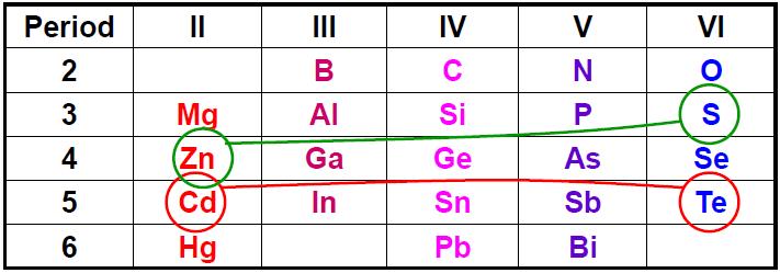
 Chapter 1 Overview of Semiconductor Materials and Physics Professor Paul K. Chu Conductivity / Resistivity of Insulators, Semiconductors, and Conductors Semiconductor Elements Period II III IV V VI 2 B
ECE 335: Electronic Engineering Lecture 2: Semiconductors
 Faculty of Engineering ECE 335: Electronic Engineering Lecture 2: Semiconductors Agenda Intrinsic Semiconductors Extrinsic Semiconductors N-type P-type Carrier Transport Drift Diffusion Semiconductors
Electro - Principles I
 Electro - Principles I Page 10-1 Atomic Theory It is necessary to know what goes on at the atomic level of a semiconductor so the characteristics of the semiconductor can be understood. In many cases a
Introduction to Semiconductor Physics. Prof.P. Ravindran, Department of Physics, Central University of Tamil Nadu, India
 Introduction to Semiconductor Physics 1 Prof.P. Ravindran, Department of Physics, Central University of Tamil Nadu, India http://folk.uio.no/ravi/cmp2013 Review of Semiconductor Physics Semiconductor fundamentals
Lecture 2. Semiconductor Physics. Sunday 4/10/2015 Semiconductor Physics 1-1
 Lecture 2 Semiconductor Physics Sunday 4/10/2015 Semiconductor Physics 1-1 Outline Intrinsic bond model: electrons and holes Charge carrier generation and recombination Intrinsic semiconductor Doping:
ECE 142: Electronic Circuits Lecture 3: Semiconductors
 Faculty of Engineering ECE 142: Electronic Circuits Lecture 3: Semiconductors Agenda Intrinsic Semiconductors Extrinsic Semiconductors N-type P-type Carrier Transport Drift Diffusion Semiconductors A semiconductor
3C3 Analogue Circuits
 Department of Electronic & Electrical Engineering Trinity College Dublin, 2014 3C3 Analogue Circuits Prof J K Vij jvij@tcd.ie Lecture 1: Introduction/ Semiconductors & Doping 1 Course Outline (subject
ELECTRONIC I Lecture 1 Introduction to semiconductor. By Asst. Prof Dr. Jassim K. Hmood
 ELECTRONIC I Lecture 1 Introduction to semiconductor By Asst. Prof Dr. Jassim K. Hmood SOLID-STATE ELECTRONIC MATERIALS Electronic materials generally can be divided into three categories: insulators,
EE143 Fall 2016 Microfabrication Technologies. Evolution of Devices
 EE143 Fall 2016 Microfabrication Technologies Prof. Ming C. Wu wu@eecs.berkeley.edu 511 Sutardja Dai Hall (SDH) 1-1 Evolution of Devices Yesterday s Transistor (1947) Today s Transistor (2006) 1-2 1 Why
1 Review of semiconductor materials and physics
 Part One Devices 1 Review of semiconductor materials and physics 1.1 Executive summary Semiconductor devices are fabricated using specific materials that offer the desired physical properties. There are
Lecture 1. OUTLINE Basic Semiconductor Physics. Reading: Chapter 2.1. Semiconductors Intrinsic (undoped) silicon Doping Carrier concentrations
 silicon Doping Carrier concentrations") Lecture 1 OUTLINE Basic Semiconductor Physics Semiconductors Intrinsic (undoped) silicon Doping Carrier concentrations Reading: Chapter 2.1 EE105 Fall 2007 Lecture 1, Slide 1 What is a Semiconductor? Low
Lecture 1 OUTLINE Basic Semiconductor Physics Semiconductors Intrinsic (undoped) silicon Doping Carrier concentrations Reading: Chapter 2.1 EE105 Fall 2007 Lecture 1, Slide 1 What is a Semiconductor? Low
ELECTRONIC DEVICES AND CIRCUITS SUMMARY
 ELECTRONIC DEVICES AND CIRCUITS SUMMARY Classification of Materials: Insulator: An insulator is a material that offers a very low level (or negligible) of conductivity when voltage is applied. Eg: Paper,
EECS143 Microfabrication Technology
 EECS143 Microfabrication Technology Professor Ali Javey Introduction to Materials Lecture 1 Evolution of Devices Yesterday s Transistor (1947) Today s Transistor (2006) Why Semiconductors? Conductors e.g
Engineering 2000 Chapter 8 Semiconductors. ENG2000: R.I. Hornsey Semi: 1
 Engineering 2000 Chapter 8 Semiconductors ENG2000: R.I. Hornsey Semi: 1 Overview We need to know the electrical properties of Si To do this, we must also draw on some of the physical properties and we
Ch. 2: Energy Bands And Charge Carriers In Semiconductors
 Ch. 2: Energy Bands And Charge Carriers In Semiconductors Discrete energy levels arise from balance of attraction force between electrons and nucleus and repulsion force between electrons each electron
Unit IV Semiconductors Engineering Physics
 Introduction A semiconductor is a material that has a resistivity lies between that of a conductor and an insulator. The conductivity of a semiconductor material can be varied under an external electrical
Lecture 2 Electrons and Holes in Semiconductors
 EE 471: Transport Phenomena in Solid State Devices Spring 2018 Lecture 2 Electrons and Holes in Semiconductors Bryan Ackland Department of Electrical and Computer Engineering Stevens Institute of Technology
Semiconductor physics I. The Crystal Structure of Solids
 Lecture 3 Semiconductor physics I The Crystal Structure of Solids 1 Semiconductor materials Types of solids Space lattices Atomic Bonding Imperfection and doping in SOLIDS 2 Semiconductor Semiconductors
Electronic Devices & Circuits
 Electronic Devices & Circuits For Electronics & Communication Engineering By www.thegateacademy.com Syllabus Syllabus for Electronic Devices Energy Bands in Intrinsic and Extrinsic Silicon, Carrier Transport,
A semiconductor is an almost insulating material, in which by contamination (doping) positive or negative charge carriers can be introduced.
 positive or negative charge carriers can be introduced.") Semiconductor A semiconductor is an almost insulating material, in which by contamination (doping) positive or negative charge carriers can be introduced. Page 2 Semiconductor materials Page 3 Energy levels
Semiconductor A semiconductor is an almost insulating material, in which by contamination (doping) positive or negative charge carriers can be introduced. Page 2 Semiconductor materials Page 3 Energy levels
Processing of Semiconducting Materials Prof. Pallab Banerji Department of Material Science Indian Institute of Technology, Kharagpur
 Processing of Semiconducting Materials Prof. Pallab Banerji Department of Material Science Indian Institute of Technology, Kharagpur Lecture - 4 Doping in Semiconductors Good morning. Let us start with
Semiconductors. Semiconductors also can collect and generate photons, so they are important in optoelectronic or photonic applications.
 Semiconductors Semiconducting materials have electrical properties that fall between true conductors, (like metals) which are always highly conducting and insulators (like glass or plastic or common ceramics)
electronics fundamentals
 electronics fundamentals circuits, devices, and applications THOMAS L. FLOYD DAVID M. BUCHLA Lesson 1: Diodes and Applications Semiconductors Figure 1-1 The Bohr model of an atom showing electrons in orbits
CLASS 1 & 2 REVISION ON SEMICONDUCTOR PHYSICS. Reference: Electronic Devices by Floyd
 CLASS 1 & 2 REVISION ON SEMICONDUCTOR PHYSICS Reference: Electronic Devices by Floyd 1 ELECTRONIC DEVICES Diodes, transistors and integrated circuits (IC) are typical devices in electronic circuits. All
Electron Energy, E E = 0. Free electron. 3s Band 2p Band Overlapping energy bands. 3p 3s 2p 2s. 2s Band. Electrons. 1s ATOM SOLID.
 Electron Energy, E Free electron Vacuum level 3p 3s 2p 2s 2s Band 3s Band 2p Band Overlapping energy bands Electrons E = 0 1s ATOM 1s SOLID In a metal the various energy bands overlap to give a single
Electronic Circuits for Mechatronics ELCT 609 Lecture 2: PN Junctions (1)
") Electronic Circuits for Mechatronics ELCT 609 Lecture 2: PN Junctions (1) Assistant Professor Office: C3.315 E-mail: eman.azab@guc.edu.eg 1 Electronic (Semiconductor) Devices P-N Junctions (Diodes): Physical
Electronic Circuits for Mechatronics ELCT 609 Lecture 2: PN Junctions (1) Assistant Professor Office: C3.315 E-mail: eman.azab@guc.edu.eg 1 Electronic (Semiconductor) Devices P-N Junctions (Diodes): Physical
EE 346: Semiconductor Devices
 EE 346: Semiconductor Devices Lecture - 6 02/06/2017 Tewodros A. Zewde 1 DENSTY OF STATES FUNCTON Since current is due to the flow of charge, an important step in the process is to determine the number
Resistance (R) Temperature (T)
 Temperature (T)") CHAPTER 1 Physical Properties of Elements and Semiconductors 1.1 Introduction Semiconductors constitute a large class of substances which have resistivities lying between those of insulators and conductors.
CHAPTER 1 Physical Properties of Elements and Semiconductors 1.1 Introduction Semiconductors constitute a large class of substances which have resistivities lying between those of insulators and conductors.
EE 5211 Analog Integrated Circuit Design. Hua Tang Fall 2012
 EE 5211 Analog Integrated Circuit Design Hua Tang Fall 2012 Today s topic: 1. Introduction to Analog IC 2. IC Manufacturing (Chapter 2) Introduction What is Integrated Circuit (IC) vs discrete circuits?
UConn ECE 4211, Semiconductor Devices and Nanostructures Lecture Week 1 January 17, 2017
 UConn ECE 411, Semiconductor Devices and Nanostructures Lecture Week 1 January 17, 017 Device Operation: One of the objectives of this course is to understand operation of carrier transport in semiconductor
EECS130 Integrated Circuit Devices
 EECS130 Integrated Circuit Devices Professor Ali Javey 8/30/2007 Semiconductor Fundamentals Lecture 2 Read: Chapters 1 and 2 Last Lecture: Energy Band Diagram Conduction band E c E g Band gap E v Valence
Charge Carriers in Semiconductor
 Charge Carriers in Semiconductor To understand PN junction s IV characteristics, it is important to understand charge carriers behavior in solids, how to modify carrier densities, and different mechanisms
ITT Technical Institute ET215 Devices I Unit 1
 ITT Technical Institute ET215 Devices I Unit 1 Chapter 1 Chapter 2, Sections 2.1-2.4 Chapter 1 Basic Concepts of Analog Circuits Recall ET115 & ET145 Ohms Law I = V/R If voltage across a resistor increases
Semiconductors 1. Explain different types of semiconductors in detail with necessary bond diagrams. Intrinsic semiconductors:
 Semiconductors 1. Explain different types of semiconductors in detail with necessary bond diagrams. There are two types of semi conductors. 1. Intrinsic semiconductors 2. Extrinsic semiconductors Intrinsic
CHAPTER 2: ENERGY BANDS & CARRIER CONCENTRATION IN THERMAL EQUILIBRIUM. M.N.A. Halif & S.N. Sabki
 CHAPTER 2: ENERGY BANDS & CARRIER CONCENTRATION IN THERMAL EQUILIBRIUM OUTLINE 2.1 INTRODUCTION: 2.1.1 Semiconductor Materials 2.1.2 Basic Crystal Structure 2.1.3 Basic Crystal Growth technique 2.1.4 Valence
CLASS 12th. Semiconductors
 CLASS 12th Semiconductors 01. Distinction Between Metals, Insulators and Semi-Conductors Metals are good conductors of electricity, insulators do not conduct electricity, while the semiconductors have
Lecture (02) Introduction to Electronics II, PN Junction and Diodes I
 Introduction to Electronics II, PN Junction and Diodes I") Lecture (02) Introduction to Electronics II, PN Junction and Diodes I By: Dr. Ahmed ElShafee ١ Agenda Current in semiconductors/conductors N type, P type semiconductors N Type Semiconductor P Type Semiconductor
Lecture (02) Introduction to Electronics II, PN Junction and Diodes I By: Dr. Ahmed ElShafee ١ Agenda Current in semiconductors/conductors N type, P type semiconductors N Type Semiconductor P Type Semiconductor
From Last Time Important new Quantum Mechanical Concepts. Atoms and Molecules. Today. Symmetry. Simple molecules.
 Today From Last Time Important new Quantum Mechanical Concepts Indistinguishability: Symmetries of the wavefunction: Symmetric and Antisymmetric Pauli exclusion principle: only one fermion per state Spin
1 Name: Student number: DEPARTMENT OF PHYSICS AND PHYSICAL OCEANOGRAPHY MEMORIAL UNIVERSITY OF NEWFOUNDLAND. Fall :00-11:00
 1 Name: DEPARTMENT OF PHYSICS AND PHYSICAL OCEANOGRAPHY MEMORIAL UNIVERSITY OF NEWFOUNDLAND Final Exam Physics 3000 December 11, 2012 Fall 2012 9:00-11:00 INSTRUCTIONS: 1. Answer all seven (7) questions.
David J. Starling Penn State Hazleton PHYS 214
 Being virtually killed by a virtual laser in a virtual space is just as effective as the real thing, because you are as dead as you think you are. -Douglas Adams, Mostly Harmless David J. Starling Penn
ECE 250 Electronic Devices 1. Electronic Device Modeling
 ECE 250 Electronic Devices 1 ECE 250 Electronic Device Modeling ECE 250 Electronic Devices 2 Introduction to Semiconductor Physics You should really take a semiconductor device physics course. We can only
Basic Semiconductor Physics
 6 Basic Semiconductor Physics 6.1 Introduction With this chapter we start with the discussion of some important concepts from semiconductor physics, which are required to understand the operation of solar
EE 446/646 Photovoltaic Devices I. Y. Baghzouz
 EE 446/646 Photovoltaic Devices I Y. Baghzouz What is Photovoltaics? First used in about 1890, the word has two parts: photo, derived from the Greek word for light, volt, relating to electricity pioneer
Electronics The basics of semiconductor physics
 Electronics The basics of semiconductor physics Prof. Márta Rencz, Gergely Nagy BME DED September 16, 2013 The basic properties of semiconductors Semiconductors conductance is between that of conductors
Free Electron Model for Metals
 Free Electron Model for Metals Metals are very good at conducting both heat and electricity. A lattice of in a sea of electrons shared between all nuclei (moving freely between them): This is referred
SEMICONDUCTOR PHYSICS
 SEMICONDUCTOR PHYSICS by Dibyendu Chowdhury Semiconductors The materials whose electrical conductivity lies between those of conductors and insulators, are known as semiconductors. Silicon Germanium Cadmium
Semiconductor Devices and Circuits Fall Midterm Exam. Instructor: Dr. Dietmar Knipp, Professor of Electrical Engineering. Name: Mat. -Nr.
 Semiconductor Devices and Circuits Fall 2003 Midterm Exam Instructor: Dr. Dietmar Knipp, Professor of Electrical Engineering Name: Mat. -Nr.: Guidelines: Duration of the Midterm: 1 hour The exam is a closed
EXTRINSIC SEMICONDUCTOR
 EXTRINSIC SEMICONDUCTOR EXTRINSIC SEMICONDUCTOR A semiconductor in which the impurity atoms are added by doping process is called Extrinsic semiconductor. The addition of impurities increases the carrier
LECTURE 23. MOS transistor. 1 We need a smart switch, i.e., an electronically controlled switch. Lecture Digital Circuits, Logic
 LECTURE 23 Lecture 16-20 Digital Circuits, Logic 1 We need a smart switch, i.e., an electronically controlled switch 2 We need a gain element for example, to make comparators. The device of our dreams
Free Electron Model for Metals
 Free Electron Model for Metals Metals are very good at conducting both heat and electricity. A lattice of in a sea of electrons shared between all nuclei (moving freely between them): This is referred
Review of Semiconductor Fundamentals
 ECE 541/ME 541 Microelectronic Fabrication Techniques Review of Semiconductor Fundamentals Zheng Yang (ERF 3017, email: yangzhen@uic.edu) Page 1 Semiconductor A semiconductor is an almost insulating material,
Calculating Band Structure
 Calculating Band Structure Nearly free electron Assume plane wave solution for electrons Weak potential V(x) Brillouin zone edge Tight binding method Electrons in local atomic states (bound states) Interatomic
n N D n p = n i p N A
 Summary of electron and hole concentration in semiconductors Intrinsic semiconductor: E G n kt i = pi = N e 2 0 Donor-doped semiconductor: n N D where N D is the concentration of donor impurity Acceptor-doped
ECE 442. Spring, Lecture -2
 ECE 442 Power Semiconductor Devices and Integrated circuits Spring, 2006 University of Illinois at Chicago Lecture -2 Semiconductor physics band structures and charge carriers 1. What are the types of
Semiconductor Physics
 Semiconductor Physics Motivation Is it possible that there might be current flowing in a conductor (or a semiconductor) even when there is no potential difference supplied across its ends? Look at the
Mat E 272 Lecture 25: Electrical properties of materials
 Mat E 272 Lecture 25: Electrical properties of materials December 6, 2001 Introduction: Calcium and copper are both metals; Ca has a valence of +2 (2 electrons per atom) while Cu has a valence of +1 (1
Introduction to Electronics and Semiconductor
 Introduction to Electronics and Semiconductor 1 Chapter Objectives To study and understand basic electronics. To study and understand semiconductor principles. 2 Definition Electronics is the branch of
5. Semiconductors and P-N junction
 5. Semiconductors and P-N junction Thomas Zimmer, University of Bordeaux, France Summary Learning Outcomes... 2 Physical background of semiconductors... 2 The silicon crystal... 2 The energy bands... 3
Semiconductors CHAPTER 3. Introduction The pn Junction with an Applied Voltage Intrinsic Semiconductors 136
 CHAPTER 3 Semiconductors Introduction 135 3.1 Intrinsic Semiconductors 136 3.2 Doped Semiconductors 139 3.3 Current Flow in Semiconductors 142 3.4 The pn Junction 148 3.5 The pn Junction with an Applied
Diodes. EE223 Digital & Analogue Electronics Derek Molloy 2012/2013.
 Diodes EE223 Digital & Analogue Electronics Derek Molloy 2012/2013 Derek.Molloy@dcu.ie Diodes: A Semiconductor? Conductors Such as copper, aluminium have a cloud of free electrons weak bound valence electrons
Electronics EC /2/2012. * In-class exams: 40% 7 th week exam 25% 12 th week exam 15%
 Arab Academy for Science, Technology and Maritime Transport Electronics EC 331 Dr. Mohamed Hassan Course Assessment * In-class exams: 40% 7 th week exam 25% 12 th week exam 15% *Tutorial exams and activities:
EE495/695 Introduction to Semiconductors I. Y. Baghzouz ECE Department UNLV
 EE495/695 Introduction to Semiconductors I Y. Baghzouz ECE Department UNLV Introduction Solar cells have always been aligned closely with other electronic devices. We will cover the basic aspects of semiconductor
Chemistry Instrumental Analysis Lecture 8. Chem 4631
 Chemistry 4631 Instrumental Analysis Lecture 8 UV to IR Components of Optical Basic components of spectroscopic instruments: stable source of radiant energy transparent container to hold sample device
Semiconductor Devices, Fall Gunnar Malm, Associate Professor Integrated Devices and Circuits, Kista Campus
 Semiconductor Devices, Fall 2014 Gunnar Malm, Associate Professor Integrated Devices and Circuits, Kista Campus gunta@kth.se, 08-790 4332 Semiconductor procesing at KTH Electrum Laboratory Stepper Lithography
The photovoltaic effect occurs in semiconductors where there are distinct valence and
 How a Photovoltaic Cell Works The photovoltaic effect occurs in semiconductors where there are distinct valence and conduction bands. (There are energies at which electrons can not exist within the solid)
1. Introduction of solid state 1.1. Elements of solid state physics:
 1. Introduction of solid state 1.1. Elements of solid state physics: To understand the operation of many of the semiconductor devices we need, at least, an appreciation of the solid state physics of homogeneous
FREQUENTLY ASKED QUESTIONS February 21, 2017
 FREQUENTLY ASKED QUESTIONS February 21, 2017 Content Questions How do you place a single arsenic atom with the ratio 1 in 100 million? Sounds difficult to get evenly spread throughout. Yes, techniques
Lecture 0. EE206 Electronics I
 Lecture 0 Course Overview EE206 Electronics I Course description: Theory, characteristics and operation of diodes, bipolar junction transistors and MOSFET transistors. When: Tue Thu 10:30-12:20 (Lectures)
KATIHAL FİZİĞİ MNT-510
 KATIHAL FİZİĞİ MNT-510 YARIİLETKENLER Kaynaklar: Katıhal Fiziği, Prof. Dr. Mustafa Dikici, Seçkin Yayıncılık Katıhal Fiziği, Şakir Aydoğan, Nobel Yayıncılık, Physics for Computer Science Students: With
The Semiconductor in Equilibrium
 Lecture 6 Semiconductor physics IV The Semiconductor in Equilibrium Equilibrium, or thermal equilibrium No external forces such as voltages, electric fields. Magnetic fields, or temperature gradients are
SEMICONDUCTORS. Conductivity lies between conductors and insulators. The flow of charge in a metal results from the
 SEMICONDUCTORS Conductivity lies between conductors and insulators The flow of charge in a metal results from the movement of electrons Electros are negatively charged particles (q=1.60x10⁻¹⁹ C ) The outermost
Semiconductor Device Physics
 1 Semiconductor Device Physics Lecture 1 http://zitompul.wordpress.com 2 0 1 3 2 Semiconductor Device Physics Textbook: Semiconductor Device Fundamentals, Robert F. Pierret, International Edition, Addison
Introduction to Engineering Materials ENGR2000. Dr.Coates
 Introduction to Engineering Materials ENGR2000 Chapter 18: Electrical Properties Dr.Coates 18.2 Ohm s Law V = IR where R is the resistance of the material, V is the voltage and I is the current. l R A
Semiconductor Physics fall 2012 problems
 Semiconductor Physics fall 2012 problems 1. An n-type sample of silicon has a uniform density N D = 10 16 atoms cm -3 of arsenic, and a p-type silicon sample has N A = 10 15 atoms cm -3 of boron. For each
* motif: a single or repeated design or color
 Chapter 2. Structure A. Electronic structure vs. Geometric structure B. Clean surface vs. Adsorbate covered surface (substrate + overlayer) C. Adsorbate structure - how are the adsorbed molecules bound
ESE 372 / Spring 2013 / Lecture 5 Metal Oxide Semiconductor Field Effect Transistor
 Metal Oxide Semiconductor Field Effect Transistor V G V G 1 Metal Oxide Semiconductor Field Effect Transistor We will need to understand how this current flows through Si What is electric current? 2 Back
Contents CONTENTS. Page 2 of 47
 J. A. Hargreaves Lockerbie Academy June 2015 Contents CONTENTS Contents... 2 CHAPTER 7 CONDUCTORS, SEMICONDUCTORS AND INSULATORS... 4 Summary of Content... 4 Summary of this chapter- notes from column
Chapter 4: Bonding in Solids and Electronic Properties. Free electron theory
 Chapter 4: Bonding in Solids and Electronic Properties Free electron theory Consider free electrons in a metal an electron gas. regards a metal as a box in which electrons are free to move. assumes nuclei
Lecture 3b. Bonding Model and Dopants. Reading: (Cont d) Notes and Anderson 2 sections
 Notes and Anderson 2 sections") Lecture 3b Bonding Model and Dopants Reading: (Cont d) Notes and Anderson 2 sections 2.3-2.7 The need for more control over carrier concentration Without help the total number of carriers (electrons and
Lecture 3b Bonding Model and Dopants Reading: (Cont d) Notes and Anderson 2 sections 2.3-2.7 The need for more control over carrier concentration Without help the total number of carriers (electrons and
Variation of Energy Bands with Alloy Composition E
 Variation of Energy Bands with Alloy Composition E 3.0 E.8.6 L 0.3eV Al x GaAs AlAs 1- xas 1.43eV.16eV X k.4 L. X.0 X 1.8 L 1.6 1.4 0 0. 0.4 0.6 X 0.8 1 1 Carriers in intrinsic Semiconductors Ec 4º 1º
Semiconductor device structures are traditionally divided into homojunction devices
 0. Introduction: Semiconductor device structures are traditionally divided into homojunction devices (devices consisting of only one type of semiconductor material) and heterojunction devices (consisting
Electrons are shared in covalent bonds between atoms of Si. A bound electron has the lowest energy state.
 Photovoltaics Basic Steps the generation of light-generated carriers; the collection of the light-generated carriers to generate a current; the generation of a large voltage across the solar cell; and
Carriers Concentration in Semiconductors - V. Prof.P. Ravindran, Department of Physics, Central University of Tamil Nadu, India
 Carriers Concentration in Semiconductors - V 1 Prof.P. Ravindran, Department of Physics, Central University of Tamil Nadu, India http://folk.uio.no/ravi/semi2013 Motion and Recombination of Electrons and
Lecture (02) PN Junctions and Diodes
 PN Junctions and Diodes") Lecture (02) PN Junctions and Diodes By: Dr. Ahmed ElShafee ١ I Agenda N type, P type semiconductors N Type Semiconductor P Type Semiconductor PN junction Energy Diagrams of the PN Junction and Depletion
Lecture (02) PN Junctions and Diodes By: Dr. Ahmed ElShafee ١ I Agenda N type, P type semiconductors N Type Semiconductor P Type Semiconductor PN junction Energy Diagrams of the PN Junction and Depletion
SEMI- CONDUCTOR PHYSICS
 C H A P T E R51 Learning Objectives The Atom Bohr's Atomic Model Electron Energy Levels in Hydrogen Atom Orbital (or Azimuthal) Quantum Number Orbital Magnetic Quantum Number (m l ) Magnetic Spin Quantum
Chapter 2. Semiconductor Fundamentals
 hapter Semiconductor Fundamentals.0 Introduction There are altogether 9 types of natural occurring elements, of which only few types are important in semiconductor physics and technology. They are the
Basic cell design. Si cell
 Basic cell design Si cell 1 Concepts needed to describe photovoltaic device 1. energy bands in semiconductors: from bonds to bands 2. free carriers: holes and electrons, doping 3. electron and hole current:
First-Hand Investigation: Modeling of Semiconductors
 perform an investigation to model the behaviour of semiconductors, including the creation of a hole or positive charge on the atom that has lost the electron and the movement of electrons and holes in
EE 346: Semiconductor Devices. 02/08/2017 Tewodros A. Zewde 1
 EE 346: Semiconductor Devices 02/08/2017 Tewodros A. Zewde 1 DOPANT ATOMS AND ENERGY LEVELS Without help the total number of carriers (electrons and holes) is limited to 2ni. For most materials, this is
Determination of properties in semiconductor materials by applying Matlab
 Determination of properties in semiconductor materials by applying Matlab Carlos Figueroa. 1, Raúl Riera A. 2 1 Departamento de Ingeniería Industrial. Universidad de Sonora A.P. 5-088, Hermosillo, Sonora.
Course overview. Me: Dr Luke Wilson. The course: Physics and applications of semiconductors. Office: E17 open door policy
 Course overview Me: Dr Luke Wilson Office: E17 open door policy email: luke.wilson@sheffield.ac.uk The course: Physics and applications of semiconductors 10 lectures aim is to allow time for at least one
Classification of Solids
 Classification of Solids Classification by conductivity, which is related to the band structure: (Filled bands are shown dark; D(E) = Density of states) Class Electron Density Density of States D(E) Examples
3.1 Introduction to Semiconductors. Y. Baghzouz ECE Department UNLV
 3.1 Introduction to Semiconductors Y. Baghzouz ECE Department UNLV Introduction In this lecture, we will cover the basic aspects of semiconductor materials, and the physical mechanisms which are at the
Lecture 7: Extrinsic semiconductors - Fermi level
 Lecture 7: Extrinsic semiconductors - Fermi level Contents 1 Dopant materials 1 2 E F in extrinsic semiconductors 5 3 Temperature dependence of carrier concentration 6 3.1 Low temperature regime (T < T
Semiconductor Physics Problems 2015
 Semiconductor Physics Problems 2015 Page and figure numbers refer to Semiconductor Devices Physics and Technology, 3rd edition, by SM Sze and M-K Lee 1. The purest semiconductor crystals it is possible
ENERGY BANDS AND GAPS IN SEMICONDUCTOR. Muhammad Hafeez Javed
 ENERGY BANDS AND GAPS IN SEMICONDUCTOR Muhammad Hafeez Javed www.rmhjaved.com rmhjaved@gmail.com Out Line Introduction Energy band Classification of materials Direct and indirect band gap of SC Classification
Chapter 1 INTRODUCTION SEMICONDUCTORS MATERIAL
 Chapter 1 INTRODUCTION TO SEMICONDUCTORS MATERIAL Objectives Discuss basic structures of atoms Discuss properties of insulators, conductors, and semiconductors Discuss covalent bonding Describe the conductions