Screening Effects in Probing the Electric Double Layer by Scanning Electrochemical Potential Microscopy (SECPM)
|
|
|
- Brian Jordan
- 5 years ago
- Views:
Transcription
 R.")
1 Presented at the COMSOL Conference 2009 Milan Screening Effects in Probing the Electric Double Layer by Scanning Electrochemical Potential Microscopy (SECPM) R. Fayçal Hamou MaxPlanckInstitut für Eisenforschung GmbH Interface Chemistry and Surface Engineering Department Atomistic Modeling Group (AMG) 1
2 V e V IHP 2 0
3 Experimental techniques Atomic force microscopy Scanning tunneling microscopy Scanning electrochemical microscopy : ECSTM, SECPM Allow electrochemists to learn more about the structure of the double layer at the atomic level. On the theoretical side, the new numerical methods of calculations provide a possibility to simulate, all the changes within the double layer. 3


4 Scanning Electrochemical Potential Microscopy (SECPM) Probing the potential profile of the EDL SECPM :Patented in


5 SECPM probe EDL Potential Profiling Electrolyte Electrode 5
6 Previous experimental results Potential profile In the SECPM experiments presented here, the decay length of the potential profile was always smaller than the Debye length from the Gouy Chapman Stern theory Debye length depends on the applied potential. Cedric Hurth; Chunzeng Li; Allen J. Bard; J. Phys. Chem. C 2007, 111,
7 SECPM probe Scanning electron micrographs of a PtIr tip prepared by the procedure described earlier in the text. at low (a) and high (b) magnification. PhD Thesis C. M. Hurth 2005 under the supervision of Prof. Allen J. Bard, The University of Texas at Austin 7
 Poisson")

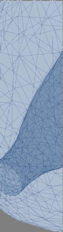
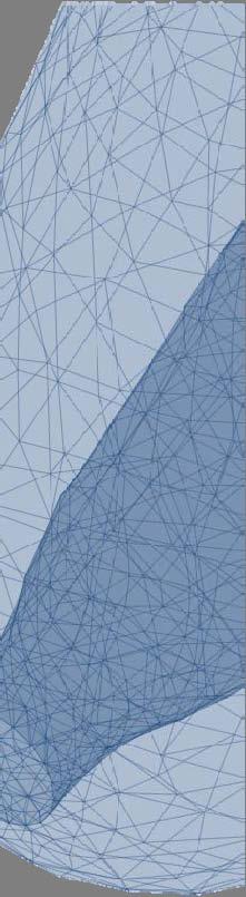
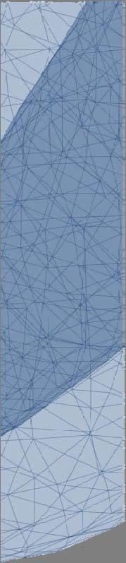
8 SECPM simulation Metallic probe Coating Electrolyte Electrode Metallic apex Using the PoissonBoltzmann for simulating the EDL (by including a Stern layer) Poisson equation to model the dielectric coating Suitable boundaries, Moving mesh, time dependent simulation: Probe moving at 10 nm/s Using Comsol Multiphysics software 8


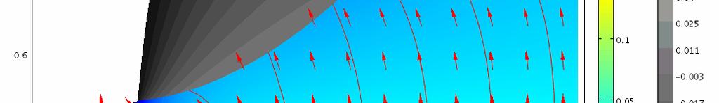
9 3D distribution of the electric field and potential 9


10 Effect of the metallic apex geometry : protruding probe Length protrusion effect 15 nm 23 nm Geometry 1 Geometry 2 11 nm Geometry 3 Quasi flat surface 2.5nm 10
11 11
12 12
13 13


14 Effect of the metallic apex geometry : protruding probe 14


15 Effect of the metallic apex geometry : protruding probe Potential profile between the Probe and the electrode for different separation distances. 15


16 Effect of the metallic apex geometry : protruding probe Geometry 2 Geometry 1 Surface charge density on the metallic protrusion 16


17 Effect of the exposed metallic surface r=8nm r=15nm r=22nm r=60nm r=30nm 17
18 18
19 19
20 Effect of the exposed metallic surface Variation of the electric flux passing through the exposed metallic tip during the approach 20
21 Effect of the exposed metallic surface Variation of the tip surface charge density during the approach 21
22 The effect of the Open Circuit Potential: Positively charged 22
23 The effect of the Open Circuit Potential: Positively charged ocp=0.148 V 23
24 The effect of the Open Circuit Potential: Positively charged ocp=0.046 V 24
25 The effect of the Open Circuit Potential: Positively charged 25
26 The effect of the Open Circuit Potential: Positively charged 26
27 The effect of the Open Circuit Potential: Positively charged 27
28 The effect of the Open Circuit Potential: Positively charged 28
29 The effect of the Open Circuit Potential: Positively charged 29
30 The effect of the Open Circuit Potential: Positively charged 30
31 The effect of the Open Circuit Potential: Positively charged Variation of the electric flux passing through the exposed metallic tip during the approach 31
32 The effect of the Open Circuit Potential: Positive charge Variation of the tip surface charge density during the approach 32
33 The effect of the Open Circuit Potential: Negatively charged ocp=0.149 V 33


34 The effect of the Open Circuit Potential: Negatively charged ocp=0.149 V 34
35 The effect of the Open Circuit Potential: Negatively charged ocp=0.045 V 35
36 The effect of the Open Circuit Potential: Negatively charged 36
37 The effect of the Open Circuit Potential: Negatively charged 37
38 The effect of the Open Circuit Potential: Negatively charged 38
39 The effect of the Open Circuit Potential: Negatively charged 39
40 The effect of the Open Circuit Potential: Negatively charged 40
41 The effect of the Open Circuit Potential: Negatively charged 41
42 The effect of the Open Circuit Potential: Negatively charged Variation of the electric flux passing through the exposed metallic tip during the approach 42
43 The effect of the Open Circuit Potential: Negatively charged Variation of the tip surface charge density during the approach 43
44 Conclusion In this investigation it was shown that the tip geometry has an influence on the probed potential. A sharp protrusion distorts the charge distribution, which can effect the probed potential considerably. A clear electrostatic screening effects was observed in probing the double layer. This effect depends on the strength of the double layer at the probe. This simulation will be extended for the surface potential mapping in order to comprehend better the importance of the effects mentioned above. 44
Supporting Information. The Study of Multireactional Electrochemical Interfaces Via a Tip Generation/Substrate
 Supporting Information The Study of Multireactional Electrochemical Interfaces Via a Tip Generation/Substrate Collection Mode of Scanning Electrochemical Microscopy The Hydrogen Evolution Reaction for
Simulating the Electrical Double Layer Guigen Zhang, Ph.D.
 Presented at the COMSOL Conference Boston Simulating the Electrical Double Layer Guigen Zhang, Ph.D. Dept. of Bioengineering, Dept. of Electrical & Computer Engineering Institute for Biological Interfaces
Probing into the Electrical Double Layer Using a Potential Nano-Probe
 A3 Foresight Program, 2. 27-3. 1, 26 Probing into the Electrical Double Layer Using a Potential Nano-Probe Heon Kang ( 姜憲 ) Department of Chemistry, Seoul National University, Republic of Korea (E-mail:
Classical Models of the Interface between an Electrode and Electrolyte. M.Sc. Ekaterina Gongadze
 Presented at the COMSOL Conference 009 Milan Classical Models of the Interface between an Electrode and Electrolyte M.Sc. Ekaterina Gongadze Faculty of Informatics and Electrical Engineering Comsol Conference
Direct Probing of Electrical Double Layers by Scanning Electrochemical Potential Microscopy
 4620 J. Phys. Chem. C 2007, 111, 4620-4627 Direct Probing of Electrical Double Layers by Scanning Electrochemical Potential Microscopy Cedric Hurth, Chunzeng Li, and Allen J. Bard*, Department of Chemistry
Real-Space Investigation of Electrical Double Layers. Potential Gradient Measurement with a Nanometer Potential Probe
 pubs.acs.org/jpcc Real-Space Investigation of Electrical Double Layers. Potential Gradient Measurement with a Nanometer Potential Probe Young-Hwan Yoon, Dae-Ha Woo, Taeho Shin, Taek Dong Chung,* and Heon
SUPPLEMENTARY INFORMATION
 The effect of particle proximity on the oxygen reduction rate of size-selected platinum clusters Markus Nesselberger 1, Melanie Roefzaad 1, R. Fayçal Hamou 2, P. Ulrich Biedermann 2, Florian F. Schweinberger
Supporting Information
 Supporting Information Detection of CO2 in the Electrochemical Reduction of Carbon Dioxide in DMF by Scanning Electrochemical Microscopy Tianhan Kai, Min Zhou, Zhiyao Duan, Graeme A. Henkelman, Allen J.
1044 Lecture #14 of 18
 Lecture #14 of 18 1044 1045 Q: What s in this set of lectures? A: B&F Chapter 13 main concepts: Section 1.2.3: Diffuse double layer structure Sections 13.1 & 13.2: Gibbs adsorption isotherm; Electrocapillary
Supplementary Information
 Supplementary Information Supplementary Figures Supplementary Figure S1. Change in open circuit potential ( OCP) of 1% W-doped BiVO 4 photoanode upon illumination with different light intensities. Above
Nanotechnology in Biological Engineering II
 Nanotechnology in Biological Engineering II THE EFFECT OF ELECTRICAL DOUBLE LAYER ON THE ELECTROCHEMICAL PROCESSES OF NANOMETER INTERDIGITATED ELECTRODES Xiaoling Yang 1 and Guigen Zhang 1,2,3 1 Micro/Nano
SUPPLEMENTARY NOTES Supplementary Note 1: Fabrication of Scanning Thermal Microscopy Probes
 SUPPLEMENTARY NOTES Supplementary Note 1: Fabrication of Scanning Thermal Microscopy Probes Fabrication of the scanning thermal microscopy (SThM) probes is summarized in Supplementary Fig. 1 and proceeds
Colloid Chemistry. La chimica moderna e la sua comunicazione Silvia Gross.
 Colloid Chemistry La chimica moderna e la sua comunicazione Silvia Gross Istituto Dipartimento di Scienze di e Scienze Tecnologie Chimiche Molecolari ISTM-CNR, Università Università degli Studi degli Studi
Simulation of Nanopores in Capacitive Energy Extraction based on Double Layer Expansion (CDLE)
") Simulation of Nanopores in Capacitive Energy Extraction based on Double Layer Expansion (CDLE) Emilio RuizReina 1, Félix Carrique 2, Ángel Delgado 3, María del Mar Fernández 3 1 Department of Applied Physics
Simulation of Nanopores in Capacitive Energy Extraction based on Double Layer Expansion (CDLE) Emilio RuizReina 1, Félix Carrique 2, Ángel Delgado 3, María del Mar Fernández 3 1 Department of Applied Physics
Supporting Information. In-Situ Detection of the Adsorbed Fe(II) Intermediate and the Mechanism of
 Intermediate and the Mechanism of") Supporting Information In-Situ Detection of the Adsorbed Fe(II) Intermediate and the Mechanism of Magnetite Electrodeposition by Scanning Electrochemical Microscopy Mohsin A Bhat, #, Nikoloz Nioradze,
Supporting Information In-Situ Detection of the Adsorbed Fe(II) Intermediate and the Mechanism of Magnetite Electrodeposition by Scanning Electrochemical Microscopy Mohsin A Bhat, #, Nikoloz Nioradze,
957 Lecture #13 of 18
 Lecture #13 of 18 957 958 Q: What was in this set of lectures? A: B&F Chapter 2 main concepts: Section 2.1 : Section 2.3: Salt; Activity; Underpotential deposition Transference numbers; Liquid junction
Electrolyte Concentration Dependence of Ion Transport through Nanochannels
 Electrolyte Concentration Dependence of Ion Transport through Nanochannels Murat Bakirci mbaki001@odu.edu Yunus Erkaya yerka001@odu.edu ABSTRACT The magnitude of current through a conical nanochannel filled
Charging Kinetics of Micropores in Supercapacitors
 Clemson University TigerPrints All Theses Theses 5-2012 Charging Kinetics of Micropores in Supercapacitors Daniel Oberklein Clemson University, dfoberklein@roadrunner.com Follow this and additional works
Supplementary Information
 Supplementary Information Supplementary Figure 1 Raman spectroscopy of CVD graphene on SiO 2 /Si substrate. Integrated Raman intensity maps of D, G, 2D peaks, scanned across the same graphene area. Scale
Analysis of Geometrical Aspects of a Kelvin Probe
 Analysis of Geometrical Aspects of a Kelvin Probe Stefan Ciba 1, Alexander Frey 2 and Ingo Kuehne* 1 1 Heilbronn University, Institute for Fast Mechatronic Systems (ISM), Kuenzelsau, Germany 2 University
Lecture 3 Charged interfaces
 Lecture 3 Charged interfaces rigin of Surface Charge Immersion of some materials in an electrolyte solution. Two mechanisms can operate. (1) Dissociation of surface sites. H H H H H M M M +H () Adsorption
Supporting Information. Three-Dimensional Super-Resolution Imaging of Single Nanoparticle Delivered by Pipettes
 Supporting Information Three-Dimensional Super-Resolution Imaging of Single Nanoparticle Delivered by Pipettes Yun Yu,, Vignesh Sundaresan,, Sabyasachi Bandyopadhyay, Yulun Zhang, Martin A. Edwards, Kim
V. Electrostatics Lecture 24: Diffuse Charge in Electrolytes
 V. Electrostatics Lecture 24: Diffuse Charge in Electrolytes MIT Student 1. Poisson-Nernst-Planck Equations The Nernst-Planck Equation is a conservation of mass equation that describes the influence of
Bruno Bastos Sales, Joost Helsen and Arne Verliefde
 FEM modeling of capacitive deionization for complex streams Dennis Cardoen Bruno Bastos Sales, Joost Helsen and Arne Verliefde International Conference on Numerical and Mathematical ing of Flow and Transport
Capacitive properties of a gold/electrolyte interface
 Capacitive properties of a gold/electrolyte interface Lab Course Manual Physik E19 (AG Krischer), Technische Universität München Abstract When metals are brought together with electrolytes, many interesting
Supplementary Figure 1. AFM scan of DPTAP bilayers. Supplementary Figure 2. Nanopipette geometry used for FEM simulations.
 Supplementary Figure 1. AFM scan of DPTAP bilayers. (a) Topography image with distinct single, double and triple layer structures. (b) Line profile corresponding to the line in (a) of a single bilayer
V. Electrostatics. MIT Student
 V. Electrostatics Lecture 26: Compact Part of the Double Layer MIT Student 1 Double-layer Capacitance 1.1 Stern Layer As was discussed in the previous lecture, the Gouy-Chapman model predicts unphysically
The Computational Simulation of the Positive Ion Propagation to Uneven Substrates
 WDS' Proceedings of Contributed Papers, Part II, 5 9,. ISBN 978-8-778-85-9 MATFYZPRESS The Computational Simulation of the Positive Ion Propagation to Uneven Substrates V. Hrubý and R. Hrach Charles University,
Application of Linear, Nonlinear and Nanoscale Conductivity Spectroscopy for Characterising Ion Transport in Solid Electrolytes
 Application of Linear, Nonlinear and Nanoscale Conductivity Spectroscopy for Characterising Ion Transport in Solid Electrolytes Bernhard Roling Institute of Physical Chemistry and Collaborative Research
Non-Faradaic Impedance Characterization of an
 Electronic Supplementary Material (ESI) for Lab on a Chip. This journal is The Royal Society of Chemistry 2014 Supplementary Information Non-Faradaic Impedance Characterization of an Evaporating Droplet
Numerical Modeling of the Bistability of Electrolyte Transport in Conical Nanopores
 Numerical Modeling of the Bistability of Electrolyte Transport in Conical Nanopores Long Luo, Robert P. Johnson, Henry S. White * Department of Chemistry, University of Utah, Salt Lake City, UT 84112,
Supplementary Information for:
 Supplementary Information for: In-situ measurement of electric-field screening in hysteresis-free PTAA/ FA.83 Cs.7 Pb(I.83 Br.7 ) 3 /C6 perovskite solar cells gives an ion mobility of ~3 x -7 cm /Vs; to
Poisson equation based modeling of DC and AC electroosmosis
 COMSOL Conference Prague 2006 Page 1 Poisson equation based modeling of DC and AC electroosmosis Michal Přibyl & Dalimil Šnita Institute of Chemical Technology, Prague, Czech Republic Department of Chemical
Electrostatic Double Layer Force: Part III
 NPTEL Chemical Engineering Interfacial Engineering Module 3: Lecture 4 Electrostatic Double Layer Force: Part III Dr. Pallab Ghosh Associate Professor Department of Chemical Engineering IIT Guwahati, Guwahati
Investigation of the diffusion of ferricyanide through porous membranes using the SECM150
 Investigation of the diffusion of ferricyanide through porous membranes using the SECM150 I INTRODUCTION Scanning ElectroChemical Microscopy (SECM) has the ability to provide spatially resolved, rather
Nanoscale work function measurements by Scanning Tunneling Spectroscopy
 Related Topics Tunneling effect, Defects, Scanning Tunneling Microscopy (STM), (STS), Local Density of States (LDOS), Work function, Surface activation, Catalysis Principle Scanning tunneling microscopy
Dependence of Potential and Ion Distribution on Electrokinetic Radius in Infinite and Finite-length Nano-channels
 Presented at the COMSOL Conference 2008 Boston Dependence of Potential and Ion Distribution on Electrokinetic Radius in Infinite and Finite-length Nano-channels Jarrod Schiffbauer *,1, Josh Fernandez 2,
Simulation of MEA in PEMFC and Interface of Nanometer-Sized Electrodes
 Presented at the COMSOL Conference 2010 China Simulation of MEA in PEMFC and Interface of Nanometer-Sized Electrodes Zhang Qianfan, Liu Yuwen, Chen Shengli * College of Chemistry and Molecular Science,
Supporting Information: Ultra-Sensitive Potentiometric Measurements of Dilute Redox Molecule
 Supporting Information: Ultra-Sensitive Potentiometric Measurements of Dilute Redox Molecule Solutions and Determination of Sensitivity Factors at Platinum Ultramicroelectrodes Stephen J. Percival and
Kevin C. Leonard and Allen J. Bard* INTRODUCTION
 pubs.acs.org/jacs The Study of Multireactional Electrochemical Interfaces via a Tip Generation/Substrate Collection Mode of Scanning Electrochemical Microscopy: The Hydrogen Evolution Reaction for Mn in
Chapter 12. Nanometrology. Oxford University Press All rights reserved.
 Chapter 12 Nanometrology Introduction Nanometrology is the science of measurement at the nanoscale level. Figure illustrates where nanoscale stands in relation to a meter and sub divisions of meter. Nanometrology
Field-Assisted Splitting of Pure Water Based on Deep-Sub-Debye-Length Nanogap Electrochemical Cells
 Field-Assisted Splitting of Pure Water Based on Deep-Sub-Debye-Length Nanogap Electrochemical Cells Yifei Wang 1, S. R. Narayanan 2 and Wei Wu 1* 1 Ming Hsieh Department of Electrical Engineering, University
Supporting Information File 1. Tunneling Ultramicroelectrode (T-UME): Nanoelectrodes and Nanoparticle Collisions
: Nanoelectrodes and Nanoparticle Collisions") Supporting Information File 1 Tunneling Ultramicroelectrode (T-UME): Nanoelectrodes and Nanoparticle Collisions Jiyeon Kim, Byung-Kwon Kim, SungKi Cho and Allen J. Bard* Center for Electrochemistry, Department
Supporting Information File 1 Tunneling Ultramicroelectrode (T-UME): Nanoelectrodes and Nanoparticle Collisions Jiyeon Kim, Byung-Kwon Kim, SungKi Cho and Allen J. Bard* Center for Electrochemistry, Department
Scanning probe studies of the electrical activity at interfaces formed by silicon wafer direct bonding
 phys. stat. sol. (c) 4, No. 8, 893 897 (007) / DOI 10.100/pssc.00675481 Scanning probe studies of the electrical activity at interfaces formed by silicon wafer direct bonding M. Ratzke *, 1,, O. Vyvenko
CZ České Budějovice, Czech Republic b Technical University of Liberec, Department of Materials Science, Hálkova 6, D Dresden, Germany
 INVESTIGATION OF ELECTRIC CONDITIONS IN THE VICINITY OF CARBON NANOTUBES GROWN IN A DC PLASMA SHEATH J. Blažek a, P. Špatenka b, Ch. Taeschner c, A. Leonhardt c a University of South Bohemia, Department
Multimedia : Boundary Lubrication Podcast, Briscoe, et al. Nature , ( )
") 3.05 Nanomechanics of Materials and Biomaterials Thursday 04/05/07 Prof. C. Ortiz, MITDMSE I LECTURE 14: TE ELECTRICAL DOUBLE LAYER (EDL) Outline : REVIEW LECTURE #11 : INTRODUCTION TO TE ELECTRICAL DOUBLE
3.05 Nanomechanics of Materials and Biomaterials Thursday 04/05/07 Prof. C. Ortiz, MITDMSE I LECTURE 14: TE ELECTRICAL DOUBLE LAYER (EDL) Outline : REVIEW LECTURE #11 : INTRODUCTION TO TE ELECTRICAL DOUBLE
Supporting information: Stability limits of tin-based electrocatalyst supports. Max-Planck-Institut für Eisenforschung GmbH, Düsseldorf, Germany
 Supporting information: Stability limits of tin-based electrocatalyst supports Simon Geiger a,*, Olga Kasian a, Andrea M. Mingers a, Karl J. J. Mayrhofer a,b,c, Serhiy Cherevko a,b,* a Department of Interface
Design of a Dielectrophoretic Based Micropipette for Gene Expression Applications Using COMSOL
 Design of a Dielectrophoretic Based Micropipette for Gene Expression Applications Using COMSOL D. Wijesinghe 1, and D. Nawarathna *1 1 Department of Electrical and Computer Engineering, North Dakota State
REPORT ON SCANNING TUNNELING MICROSCOPE. Course ME-228 Materials and Structural Property Correlations Course Instructor Prof. M. S.
 REPORT ON SCANNING TUNNELING MICROSCOPE Course ME-228 Materials and Structural Property Correlations Course Instructor Prof. M. S. Bobji Submitted by Ankush Kumar Jaiswal (09371) Abhay Nandan (09301) Sunil
Contents. Preface XI Symbols and Abbreviations XIII. 1 Introduction 1
 V Contents Preface XI Symbols and Abbreviations XIII 1 Introduction 1 2 Van der Waals Forces 5 2.1 Van der Waals Forces Between Molecules 5 2.1.1 Coulomb Interaction 5 2.1.2 Monopole Dipole Interaction
Scanning Probe Microscopy. EMSE-515 F. Ernst
 Scanning Probe Microscopy EMSE-515 F. Ernst 1 Literature 2 3 Scanning Probe Microscopy: The Lab on a Tip by Ernst Meyer,Ans Josef Hug,Roland Bennewitz 4 Scanning Probe Microscopy and Spectroscopy : Theory,
Chapter-II CHEMISTRY OF PHOTOELECTRODE- ELECTROLYTE INTERFACE
 z Chapter-II CHEMISTRY OF PHOTOELECTRODE- ELECTROLYTE INTERFACE 2.1 Introduction In recent years, semiconductor-electrolyte cells have been attracting a great deal of interest in the field of solar energy
Supplementary Information for
 Electronic Supplementary Material (ESI) for Physical Chemistry Chemical Physics. This journal is the Owner Societies 014 Supplementary Information for High Resolution Mapping of Oxygen Reduction Reaction
Charging and Transport Dynamics of a Flow-
 Charging and Transport Dynamics of a Flow- Through Electrode Capacitive Deionization System Supporting information Yatian Qu, a,b Patrick G. Campbell, b Ali Hemmatifar, a Jennifer M. Knipe, b Colin K.
Basic Laboratory. Materials Science and Engineering. Atomic Force Microscopy (AFM)
") Basic Laboratory Materials Science and Engineering Atomic Force Microscopy (AFM) M108 Stand: 20.10.2015 Aim: Presentation of an application of the AFM for studying surface morphology. Inhalt 1.Introduction...
Basic Laboratory Materials Science and Engineering Atomic Force Microscopy (AFM) M108 Stand: 20.10.2015 Aim: Presentation of an application of the AFM for studying surface morphology. Inhalt 1.Introduction...
Diffuse-charge effects on the transient response of electrochemical cells
 Diffuse-charge effects on the transient response of electrochemical cells M. van Soestbergen,,2 P. M. Biesheuvel, 3 and M. Z. Bazant 4 Materials Innovation Institute, Mekelweg 2, 2628 CD Delft, The Netherlands
Structure and charging kinetics of electrical double layers at large electrode voltages
 Microfluid Nanofluid (21) 8:73 78 DOI 1.17/s144-9-542-2 SHORT COMMUNICATION Structure and charging kinetics of electrical double layers at large electrode voltages Clint Cagle Guang Feng Rui Qiao Jingsong
Plasma Modeling with COMSOL Multiphysics
 Plasma Modeling with COMSOL Multiphysics Copyright 2014 COMSOL. Any of the images, text, and equations here may be copied and modified for your own internal use. All trademarks are the property of their
Scanning Tunneling Microscopy: theory and examples
 Scanning Tunneling Microscopy: theory and examples Jan Knudsen The MAX IV laboratory & Division of synchrotron radiation research K5-53 (Sljus) jan.knudsen@sljus.lu.se April 17, 018 http://www.sljus.lu.se/staff/rainer/spm.htm
Scanning Probe Microscopy (SPM)
") Scanning Probe Microscopy (SPM) Scanning Tunneling Microscopy (STM) --- G. Binnig, H. Rohrer et al, (1982) Near-Field Scanning Optical Microscopy (NSOM) --- D. W. Pohl (1982) Atomic Force Microscopy (AFM)
Scanning Probe Microscopy (SPM) Scanning Tunneling Microscopy (STM) --- G. Binnig, H. Rohrer et al, (1982) Near-Field Scanning Optical Microscopy (NSOM) --- D. W. Pohl (1982) Atomic Force Microscopy (AFM)
Next layer is called diffuse layer----ions not held tightly----thickness is > 1000 angstroms-- exact distance depends on ionic strength of soln
 What does double layer of IPE look like?-see Fig.1.2.3 Also called Electrified Inteface At no external E appl -- inner Stern layer or Inner Helmholz plane (IHP) contains mostly solvent solvent molecules
Scanning Force Microscopy
 Scanning Force Microscopy Roland Bennewitz Rutherford Physics Building 405 Phone 398-3058 roland.bennewitz@mcgill.ca Scanning Probe is moved along scan lines over a sample surface 1 Force Microscopy Data
Supporting Information. Electrochemical Vapor Deposition (E-CVD) of Semiconductors from Gas. Phase with a Solid Membrane Cell
 of Semiconductors from Gas. Phase with a Solid Membrane Cell") Supporting Information Electrochemical Vapor Deposition (E-CVD) of Semiconductors from Gas Phase with a Solid Membrane Cell Sung Ki Cho 1, Fu-Ren F. Fan, and Allen J. Bard * Center for Electrochemistry,
Supporting Information Electrochemical Vapor Deposition (E-CVD) of Semiconductors from Gas Phase with a Solid Membrane Cell Sung Ki Cho 1, Fu-Ren F. Fan, and Allen J. Bard * Center for Electrochemistry,
Copyright. Joaquin Rodriguez Lopez
 Copyright by Joaquin Rodriguez Lopez 2010 The Dissertation Committee for Joaquin Rodriguez Lopez Certifies that this is the approved version of the following dissertation: The Use of Scanning Electrochemical
Ion Concentration and Electromechanical Actuation Simulations of Ionic Polymer-Metal Composites
 October 5-7, 2016, Boston, Massachusetts, USA Ion Concentration and Electromechanical Actuation Simulations of Ionic Polymer-Metal Composites Tyler Stalbaum, Qi Shen, and Kwang J. Kim Active Materials
Short communication On Asymmetric Shape of Electric Double Layer Capacitance Curve
 Int. J. Electrochem. Sci., 10 (015) 1-7 International Journal of ELECTROCHEMICAL SCIENCE www.electrochemsci.org Short communication On Asymmetric Shape of Electric Double Layer Capacitance Curve Aljaž
Supporting Information. 15 January, Ms. ID: ac b. Parallel Screening of Electrocatalyst Candidates using Bipolar
 Supporting Information 15 January, 2013 Ms. ID: ac-2012-03581b Parallel Screening of Electrocatalyst Candidates using Bipolar Electrochemistry Stephen E. Fosdick, Sean P. Berglund, C. Buddie Mullins, and
Scanning electrochemical microscopy (SECM) is a wellestablished
 is a wellestablished") pubs.acs.org/ac Electrophoretic Migration and Particle Collisions in Scanning Electrochemical Microscopy Aliaksei Boika and Allen J. Bard* Center for Electrochemistry, Department of Chemistry and Biochemistry,
pubs.acs.org/ac Electrophoretic Migration and Particle Collisions in Scanning Electrochemical Microscopy Aliaksei Boika and Allen J. Bard* Center for Electrochemistry, Department of Chemistry and Biochemistry,
NTEGRA for EC PRESENTATION
 NTEGRA for EC PRESENTATION Application Purpose: In-situ control/modification of the surface morphology of single crystal and polycrystal electrodes (samples) during electrochemical process (in situ) in
Mikaël Cugnet, Issam Baghdadi, and Marion Perrin OCTOBER 10, Excerpt from the Proceedings of the 2012 COMSOL Conference in Milan
 Mikaël Cugnet, Issam Baghdadi, and Marion Perrin OCTOBER 0, 202 Comsol Conference Europe 202, Milan, CEA Italy 0 AVRIL 202 PAGE Excerpt from the Proceedings of the 202 COMSOL Conference in Milan SUMMARY
Spatially resolving density-dependent screening around a single charged atom in graphene
 Supplementary Information for Spatially resolving density-dependent screening around a single charged atom in graphene Dillon Wong, Fabiano Corsetti, Yang Wang, Victor W. Brar, Hsin-Zon Tsai, Qiong Wu,
3D modeling of Electrical Field and Electrical Potential in different contamination condition in Polymeric Insulator
 3D modeling of Electrical Field and Electrical Potential in different contamination condition in Polymeric Insulator A. Majzoobi *, I. A. Joneidi, S. Mohajer, H.Mohseni, A. A. Shayegani High Voltage Lab,
Surface Complexation.
 Surface Complexation. Jean-François Gaillard, Notes for CE-367 OBJECTIVES To show how the presence of particles in natural and engineered systems controls the fate of many trace elements. The concepts
Adaptive numerical simulation of Streamer. Shailendra Singh
 Adaptive numerical simulation of Streamer Shailendra Singh Tools: BDV from Drift diffusion calculation Motivation: Streamer criteria works very well in moderately uniform field. But in highly non uniform
Figure S1 TEM image of nanoparticles, showing the hexagonal shape of the particles.
 Electronic Supplementary Material (ESI) for Journal of Materials Chemistry A. This journal is The Royal Society of Chemistry 2014 Electronic Supplementary Information Au@Poly(acrylic acid) Plasmons and
Modelling the Static and Dynamic Behaviour of Electrolytes: A Modified Poisson-Nernst-Planck Approach
 Modelling the Static and Dynamic Behaviour of Electrolytes: A Modified Poisson-Nernst-Planck Approach A thesis submitted to the University of Manchester for the degree of Doctor of Philosophy in the Faculty
Chapter 10. Nanometrology. Oxford University Press All rights reserved.
 Chapter 10 Nanometrology Oxford University Press 2013. All rights reserved. 1 Introduction Nanometrology is the science of measurement at the nanoscale level. Figure illustrates where nanoscale stands
Charged Interfaces & electrokinetic
 Lecture Note #7 Charged Interfaces & electrokinetic phenomena Reading: Shaw, ch. 7 Origin of the charge at colloidal surfaces 1. Ionization Proteins acquire their charge by ionization of COOH and NH 2
Atomic Force Microscopy and Real Atomic Resolution. Simple Computer Simulations.
 EUROPHYSICS LETTERS Europhys. Lett., 26 (2), pp. 103-107 (1994) 10 April 1994 Atomic Force Microscopy and Real Atomic Resolution. Simple Computer Simulations. V. KOUTSOS, E. MANIAS, G. TEN BRINKE and G.
Supporting Information. Single Particle Detection by Area Amplification Single Wall Carbon Nanotube Attachment to a Nanoelectrode
 Supporting Information Single Particle Detection by Area Amplification Single Wall Carbon Nanotube Attachment to a Nanoelectrode Jun Hui Park, Scott N. Thorgaard, Bo Zhang, Allen J. Bard * Center for Electrochemistry,
Simulation of Turbulent Flow of a Rotating Cylinder Electrode. Influence of Using Plates and Concentric Cylinder as Counter Electrodes
 Int. J. Electrochem. Sci., 8 (2013) 4690-4699 International Journal of ELECTROCHEMICAL SCIENCE www.electrochemsci.org Simulation of Turbulent Flow of a Rotating Cylinder Electrode. Influence of Using Plates
Curriculum Vitae December 2006
 Appendix: (A brief description of some representative results) (1) Electronic states of Pb adatom and Pb adatom chains on Pb(111) have been investigated by spatially scanning tunneling spectroscopy (STS)
Specific ion effects on the interaction of. hydrophobic and hydrophilic self assembled
 Supporting Information Specific ion effects on the interaction of hydrophobic and hydrophilic self assembled monolayers T. Rios-Carvajal*, N. R. Pedersen, N. Bovet, S.L.S. Stipp, T. Hassenkam. Nano-Science
Figure 2: Simulation results of concentration by line scan along the x-axis at different partitioning coefficients after 0.48 ms.
 Executive Summary One of the critical hurdles of the success of many clean energy technologies is energy storage. For this, new and advanced computational tools to predict battery properties are very important.
Experimental Observation of Nonlinear Ionic Transport at the Nanometer Scale
 Experimental Observation of Nonlinear Ionic Transport at the Nanometer Scale NANO LETTERS 2006 Vol. 6, No. 11 2531-2535 Diego Krapf, Bernadette M. Quinn, Meng-Yue Wu, Henny W. Zandbergen, Cees Dekker,
Generalization of Gouy-Chapman-Stern Model of Electric Double Layer for a Morphologically Complex Electrode: Deterministic and Stochastic Morphology
 Chapter 3 Generalization of Gouy-Chapman-Stern Model of Electric Double Layer for a Morphologically Complex Electrode: Deterministic and Stochastic Morphology All generalizations are dangerous, even this
Supporting Information
 Supporting Information Electrogenerated Chemiluminescence of Single Conjugated Polymer Nanoparticles Ya-Lan Chang, Rodrigo E. Palacios, Fu-Ren F. Fan, Allen J. Bard, and Paul F. Barbara Department of Chemistry
Theory of Charge Transport in Mixed Conductors: Description of Interfacial Contributions Compatible with the Gibbs Thermodynamics
 Theory of Charge Transport in Mixed Conductors: Description of Interfacial Contributions Compatible with the Gibbs Thermodynamics Mikhail A. Vorotyntsev LSEO-UMR 5188 CNRS, Université de Bourgogne, Dijon,
Supplementary Figures
 Supplementary Figures Supplementary Figure 1. AFM profiles of the charge transport and perovskite layers. AFM Image showing the thickness (y axis) of the layer with respect to the horizontal position of
Nanoscale characteristics by Scanning Tunneling Spectroscopy
 Related Topics Tunneling effect, Scanning Tunneling Microscopy (STM), (STS), Local Density of States (LDOS), Band structure, Band Gap, k-space, Brioullin Zone, Metal, Semi-Metal, Semiconductor Principle
Two-Electrode Measurements Of Electrostatic Double Layer Potentials With Atomic Force Microscopy
 University of South Carolina Scholar Commons Theses and Dissertations 2018 Two-Electrode Measurements Of Electrostatic Double Layer Potentials With Atomic Force Microscopy Jason Giamberardino University
Yin-Quan Li, Orawon Chailapakul, and Richard M. Crooks a) Department of Chemistry, Texas A&M University, College Station, Texas
 Department of Chemistry, Texas A&M University, College Station, Texas") Electrochemical scanning tunneling microscopy study of the electrochemical behavior of naked and n-alkanethiol-modified Au(111) surfaces in F - and CN -containing electrolyte solutions Yin-Quan Li, Orawon
Electrochemical scanning tunneling microscopy study of the electrochemical behavior of naked and n-alkanethiol-modified Au(111) surfaces in F - and CN -containing electrolyte solutions Yin-Quan Li, Orawon
Università degli Studi di Bari "Aldo Moro"
 Università degli Studi di Bari "Aldo Moro" Table of contents 1. Introduction to Atomic Force Microscopy; 2. Introduction to Raman Spectroscopy; 3. The need for a hybrid technique Raman AFM microscopy;
General concept and defining characteristics of AFM. Dina Kudasheva Advisor: Prof. Mary K. Cowman
 General concept and defining characteristics of AFM Dina Kudasheva Advisor: Prof. Mary K. Cowman Overview Introduction History of the SPM invention Technical Capabilities Principles of operation Examples
Ultrafast nanophotonics - optical control of coherent electron -
 ICTP 18.2.8 Ultrafast nanophotonics - optical control of coherent electron - Hirofumi Yanagisawa LMU, MPQ Hirofumi Yanagisawa Japan (Tokyo) Switzerland (Zurich) Germany (Munich) http://roundtripticket.me/world-map-labled.html/best-image-of-diagram-world-map-and-labeled-for-labled
Supporting Information for
 Supporting Information for Electrodeposition of Isolated Platinum Atoms and Clusters on Bismuth Characterization and Electrocatalysis Min Zhou, Jeffrey E. Dick, and Allen J. Bard Center for Electrochemistry,
EMISSION OF QD IN ELECTROSTATIC FIELDS
 EMISSION OF QD IN ELECTROSTATIC FIELDS P. Hruska, L. Grmela Physics Department, FEEC, Brno University of Technology Abstract The paper presents the wave functions ψ, probability functions ψψ* and the ground
Joshua Whittam, 1 Andrew L. Hector, 1 * Christopher Kavanagh, 2 John R. Owen 1 and Gillian Reid 1
 Supporting Information: Combination of Solid State and Electrochemical Impedance Spectroscopy to Explore Effects of Porosity in Sol-Gel Derived BaTiO3 Thin Films Joshua Whittam, 1 Andrew L. Hector, 1 *
Single Molecule Electrochemistry on a Porous Silica-Coated Electrode
 Supporting information for Single Molecule Electrochemistry on a Porous Silica-Coated Electrode Jin Lu, Yunshan Fan, Marco Howard, Joshua C. Vaughan, and Bo Zhang* Department of Chemistry, University of
Supplementary Figure 2 Photoluminescence in 1L- (black line) and 7L-MoS 2 (red line) of the Figure 1B with illuminated wavelength of 543 nm.
 and 7L-MoS 2 (red line) of the Figure 1B with illuminated wavelength of 543 nm.") PL (normalized) Intensity (arb. u.) 1 1 8 7L-MoS 1L-MoS 6 4 37 38 39 4 41 4 Raman shift (cm -1 ) Supplementary Figure 1 Raman spectra of the Figure 1B at the 1L-MoS area (black line) and 7L-MoS area (red
PL (normalized) Intensity (arb. u.) 1 1 8 7L-MoS 1L-MoS 6 4 37 38 39 4 41 4 Raman shift (cm -1 ) Supplementary Figure 1 Raman spectra of the Figure 1B at the 1L-MoS area (black line) and 7L-MoS area (red