Ultrafast nanophotonics - optical control of coherent electron -
|
|
|
- Elisabeth Parks
- 5 years ago
- Views:
Transcription


1 ICTP Ultrafast nanophotonics - optical control of coherent electron - Hirofumi Yanagisawa LMU, MPQ
 Germany (Munich)")

2 Hirofumi Yanagisawa Japan (Tokyo) Switzerland (Zurich) Germany (Munich)
3 Laser-induced electron emission from a metallic tip
4 Slow response Phonon system nano-, pico- sec Ultrafast response Electronic system femto-, atto- sec CW laser Pulse Laser (ps) Pulse Laser (fs) 5 Nature series 10 PRL PRL 30, 1193 Nucl. Instr. And Meth. A 256,191 PRL 96,


5 Ultrafast nanophotonics? Time Size nm um mm m Size atto-femto Here! pico-nano milli-sec Time

6 Ultrafast nanophotonics Light Nano structure
7
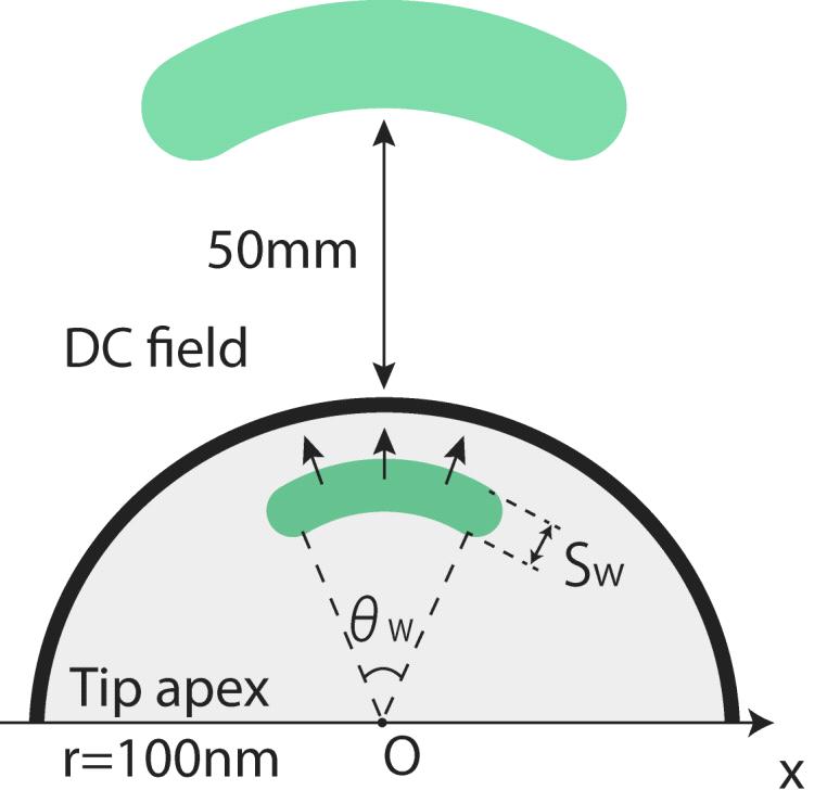
8 k Nano-sphere r=100nm ~wavelength (800nm)
9 sec Atto Femto Pico Nano Electron Phonon (lattice) 1st 2nd 2nd Plasmonics Tunnelling Rescattering Quiver Sub-cycle Weak field Laser absorption El-El scattering (heating El) El-Ph scattering (heating Ph) Phase transition Coherent phonon Surface Diffusion Melting Strong field El: Electron Ph: Phonon

10 Sphere Nano-structures Star Tip Adv. Mater. 26, 2353 Bowtie
11 Laser-induced electron emission from a metallic tip
12 Reference books - Principles of Nano-Optics Novotny and Hecht - Physics of Surface and Interfaces Harald Ibach - Field Emission and Field Ionization Robert Gomer
13 We learn today 1. Characeterization of tip apex 2. Beauty of nanophotonics in laser-induced electron emission from tip 3. Optical control of coherent electron wave
14 Let s learn more about tip and electron emission Why electron source?


15 1nm = 10-9 m Electron Electron Microscopy Best probe for Nano-object Electron gun Nano-object Detector Atom The TEM picture is taken from

 1fs =")


16 Introduction 2 Electron gun- M. Aeschlimann, Nature 446, 301 (2007) 1fs = sec Space 3D Dynamical information New Phenomena Coherence Laser pulse Electron gun ~100nm and ~100fs Tip Time Pulsed laser Brightness lens Tip B. Cho, PRL 92, (2004) C. Oshima, Nature 396, 557 (1998) ~1fs P. Hommelhoff, PRL 96, (2006)
17 How can we get electrons? Surface and work function

18 Work function Work functions Ionization Energy (surface) (atom) E vac 2-6eV Work function Φ E F Vacuum Metal Change surface to surface
 5.")
19 How can we get electrons? 1. Thermal emission 2. Photoemission 3. Field emission 4. Photo-field emission (fs) 5. Optical field emission (as)
20 How can we get electrons? e -x Thermionic emission Photoemission E vac E vac photon E F E F J T 2 exp(-φ/kt) J I n (n order photon)

21 Metal Vacuum Field emission Nanometer sharpness Mesh Grid -1~-2kV Tip E F Surface Barrier
22 How thin barrier has to be? F=3-6V/nm Φ 3-6eV E F Metal Vacuum ~1nm J F 2 exp(-aφ 3/2 /bf)


23 Photo-field emission photoemission optical fieldemission E F hν hν hν E E x x Weak field Strong field
24 Various way to characterize tip apex
25 1 Langmuir 10-6 mbar x 1 second 1.6eV!! Photon and Particle Interactions with Surfaces in Space Volume 37 of the series Astrophysics and Space Science Library pp M. Bujor

26 How to make and keep clean surface? Ar + Ar + 1 Langmuir 10-6 mbar x second Ar mbar -> 1 sec 10-7 mbar -> 10 sec 10-8 mbar -> 2 min 10-9 mbar -> 20 min Heating mbar -> 3 hr
 Around 1935 2. Field ion microscopy (FIM) Around 1950 individual atoms and their arrangement. 3.")
27 Characterization of tip apex First time in history, Erwin Mueller (German physist) A Biographical Memoir Vol 82 by ALLAN J. MELMED 1. Field emission microscopy (FEM) Around Field ion microscopy (FIM) Around 1950 individual atoms and their arrangement. 3. Atom probe field ion microscopy (APFIM)
28 Field Emission and Field Ionization: Robert Gomer FEM Magnification: x/br b~
 (310)(011)(310) (111) Radius ~ 100nm")
29 Field emission pattern with and without laser Intensity high Without laser Field Emission and Field Ionization: Robert Gomer low Tungsten Tip Vtip=-2250V (111) (310)(011)(310) (111) Radius ~ 100nm Side
![Various Field emission image from W[011] N 2 Clean Phys. Rev.](/docs-images/93/113413684/images/30-0.jpg "Lett. 45, 1856 (1980).")
30 Various Field emission image from W[011] N 2 Clean Phys. Rev. Lett. 45, 1856 (1980). O 2 FEM pattern change depending on adsorbate

31 Graphene Simulation, Edited by Jian Ru Gong, ISBN Spatial resolution => 1 2nm


32 Power of FEM FEM View from V tip =-900V Nano-tip?


33 Power of FEM Nano-tip? FEM V tip =-900V

34 Positive bias Positively charged
35
 Mesh Grid y Air Vacuum (UHV) Lens : f=15mm Oscillator 800nm,")
 PC Sample :")
36 Experimental set up Field Emission Microscopy Resistive anode MCP (Chevron) Mesh Grid y Air Vacuum (UHV) Lens : f=15mm Oscillator 800nm, 76MHz, 55fs Laser Polarization θ p Heating φ θ y High voltage Pre amplifier Position computer focus 4μm z x (negative) PC Sample : Tungsten wire

 Radius ~ 100nm")
 Side Vtip=-2250V")
37 Field emission pattern with and without laser Intensity high Without laser With laser (800nm) low 30nm (111) Radius ~ 100nm Tungsten Tip (310)(011)(310) P L =20mW (111) Side Vtip=-2250V Vtip=-1600V
38 What is physics behind?

39 Surface electromagnetic wave Electromagnetic wave couples with surface charge Surface plasmon polariton: Epsilon_R <0 Zenneck wave : Epsilon_R >0, Epsilon_Im >>0 Phys. Rev. B 44, 5855 (1991).


40 Propagation of surface electromagnetic waves Propagation of Laser E k Photo-field Time average emission Rapex =100nm MaX-1: C. Hafner With laser k Max θ p =0 θ p =30 θ p =60 θ p =90 θ p =120 θ p =150 Min


41 Let s simulate laser-induced field emission images
 FEM j exp F DC E vac")

42 Simulation of LFEM (photo-field emission model) FEM j exp F DC E vac F=F DC Work function e - E F j exp -j calc =0 Φ MaX-1: C. Hafner Photo-field Field emission


 E F jcalc LFEM")
43 Simulation of LFEM (photo-field emission model) FEM F DC F laser E vac e - F 2 laser hν j exp -j calc =0 Φ, F DC f(e) E F jcalc LFEM Photo-field emission
44 Simulations : Photo-field emission model PRL 103, (2009) θ p =0 θ p =30 θ p =60 Exp. Exp. Experiment Simulation Sim. Sim. Exp. θ p =90 θ p =120 θ p =150 Exp. Exp. Sim. Sim. Sim. Top

45 Q1: Upon laser irradiation, which side of apex will be hotter, laser exposed side or shadow side? Time ave. With laser k


46 E field Deposited energy J/cm 3 Electron Temp. Phys. Rev. B 86, (2012)

47 What s nice? Tip Coherence length ~200nm Spatio-temporal control of coherent electron emission Coherence time ~200fs At 30K Coherence length ~10nm At room temperature B. Cho, Phys. Rev. Lett. 92, (2004)
48 Optical control of Young s interference
 (310) (310) (111)")
49 Without laser With laser (7fs, 40mW) Interference (111) (310) (310) (111)

50 Polarization dependence of interference pattern Pol=10 Pol=40 C C D A B A Interference Pol=90 Pol=110 A-B C-D B B A
51 Data analysis: Gaussian fitting Pol= x Line profile L I S L I S x Gaussian fitting

52 Polarization dependence of electron 1 intensity x L S I 2*(L*S) 0.5 L+S 0.01 x x Polarization angle (degree) L L S 2*(L*S) 0.5 (A+B) 2 =A 2 +B 2 +2AB I S


53 Simulations : Interference Far field Potential landscape 2D TDSE (013) (111) Interference peak
 Energy")
54 Simulations : Energy dependence of interference Scientific Reports 7, (2017) Energy Dependence
55 Transmission Probability Q2: Do we need quantum mechanical treatment for transmission probability of photoemission? E F Photo-field emission hν hν hν Photoemission E Photoemission E vac Photon x E F
56 DeVries, P. L. A First Course in Computational Physics (John Wiley & Sons, Inc., 1994) 9eV Electron 10eV 0eV Surface

57 Electron 11eV 10eV 0eV Surface
58 Electron 15eV 10eV 0eV Surface
59 Time-resolved electron holography k k Delay line

60 ? k A B k Delay line Beam Splitter Such a dense electron source cannot be available.

61 Summary Introduction of myself Electron emission from a nano-tip How can we get electrons? -work function -various ways to emit electrons How to characterize tip apex: FEM Laser-induced field emission Site-selective technique Optical control of Young s interference

62 Tomorrow More about electron dynamics
SUPPLEMENTARY INFORMATION
 doi:1.138/nature1878 I. Experimental setup OPA, DFG Ti:Sa Oscillator, Amplifier PD U DC U Analyzer HV Energy analyzer MCP PS CCD Polarizer UHV Figure S1: Experimental setup used in mid infrared photoemission
MSE 321 Structural Characterization
 Optical Microscope Plan Lenses In an "ideal" single-element lens system all planar wave fronts are focused to a point at distance f from the lens; therefore: Image near the optical axis will be in perfect
tip conducting surface
 PhysicsAndMathsTutor.com 1 1. The diagram shows the tip of a scanning tunnelling microscope (STM) above a conducting surface. The tip is at a potential of 1.0 V relative to the surface. If the tip is sufficiently
Elastic Constants and Microstructure of Amorphous SiO 2 Thin Films Studied by Brillouin Oscillations
 1st International Symposium on Laser Ultrasonics: Science, Technology and Applications July 16-18 2008, Montreal, Canada Elastic Constants and Microstructure of Amorphous SiO 2 Thin Films Studied by Brillouin
Laser matter interaction
 Laser matter interaction PH413 Lasers & Photonics Lecture 26 Why study laser matter interaction? Fundamental physics Chemical analysis Material processing Biomedical applications Deposition of novel structures
Ecole Franco-Roumaine : Magnétisme des systèmes nanoscopiques et structures hybrides - Brasov, Modern Analytical Microscopic Tools
 1. Introduction Solid Surfaces Analysis Group, Institute of Physics, Chemnitz University of Technology, Germany 2. Limitations of Conventional Optical Microscopy 3. Electron Microscopies Transmission Electron
Ultrafast X-Ray-Matter Interaction and Damage of Inorganic Solids October 10, 2008
 Ultrafast X-Ray-Matter Interaction and Damage of Inorganic Solids October 10, 2008 Richard London rlondon@llnl.gov Workshop on Interaction of Free Electron Laser Radiation with Matter Hamburg This work
= 6 (1/ nm) So what is probability of finding electron tunneled into a barrier 3 ev high?
 So what is probability of finding electron tunneled into a barrier 3 ev high?") STM STM With a scanning tunneling microscope, images of surfaces with atomic resolution can be readily obtained. An STM uses quantum tunneling of electrons to map the density of electrons on the surface
STM STM With a scanning tunneling microscope, images of surfaces with atomic resolution can be readily obtained. An STM uses quantum tunneling of electrons to map the density of electrons on the surface
h p λ = mν Back to de Broglie and the electron as a wave you will learn more about this Equation in CHEM* 2060
 Back to de Broglie and the electron as a wave λ = mν h = h p you will learn more about this Equation in CHEM* 2060 We will soon see that the energies (speed for now if you like) of the electrons in the
MeV electron diffraction and microscopy
 UESDM, UCLA, Dec. 12 14, 2012 MeV electron diffraction and microscopy in Osaka University Jinfeng Yang Osaka University, Japan Collaborators: (RIKEN) Yoshie Murooka (Osaka Univ.) Y. Naruse, K. Kan, K.
ρ. Photoemission is presumed to occur if the photon energy is enough to raise qf πε, where q is the electron charge, F the electric field, and ε 0 φ ω
 Pulsed photoelectric field emission from needle cathodes C. Hernandez Garcia and C. A. Brau Vanderbilt University, Department of Physics, Nashville, TN 37235, USA Experiments have been carried out to measure
Recent Status of Polarized Electron Sources at Nagoya University
 Recent Status of Polarized Electron Sources at Nagoya University M. Kuwahara, N. Yamamoto, F. Furuta, T. Nakanishi, S. Okumi, M. Yamamoto, M. Kuriki *, T. Ujihara ** and K. Takeda ** Graduate School of
Optical Spectroscopy of Advanced Materials
 Phys 590B Condensed Matter Physics: Experimental Methods Optical Spectroscopy of Advanced Materials Basic optics, nonlinear and ultrafast optics Jigang Wang Department of Physics, Iowa State University
Imaging Methods: Scanning Force Microscopy (SFM / AFM)
") Imaging Methods: Scanning Force Microscopy (SFM / AFM) The atomic force microscope (AFM) probes the surface of a sample with a sharp tip, a couple of microns long and often less than 100 Å in diameter.
Imaging Methods: Scanning Force Microscopy (SFM / AFM) The atomic force microscope (AFM) probes the surface of a sample with a sharp tip, a couple of microns long and often less than 100 Å in diameter.
STRONG DOUBLE LAYER STRUCTURE IN THERMIONIC VACUUM ARC PLASMA *
 STRONG DOUBLE LAYER STRUCTURE IN THERMIONIC VACUUM ARC PLASMA * V. TIRON 1, L. MIHAESCU 1, C.P. LUNGU 2 and G. POPA 1 1 Faculty of Physics, Al. I. Cuza University, 700506, Iasi, Romania 2 National Institute
Modeling Electron Emission From Diamond-Amplified Cathodes
 Modeling Electron Emission From Diamond-Amplified Cathodes D. A. Dimitrov Tech-X Corporation, Boulder, CO I. Ben-Zvi, T. Rao, J. Smedley, E. Wang, X. Chang Brookhaven National Lab, NY This work is funded
Nanophysics: Main trends
 Nano-opto-electronics Nanophysics: Main trends Nanomechanics Main issues Light interaction with small structures Molecules Nanoparticles (semiconductor and metallic) Microparticles Photonic crystals Nanoplasmonics
1 Mathematical description of ultrashort laser pulses
 1 Mathematical description of ultrashort laser pulses 1.1 We first perform the Fourier transform directly on the Gaussian electric field: E(ω) = F[E(t)] = A 0 e 4 ln ( t T FWHM ) e i(ω 0t+ϕ CE ) e iωt
Needle cathodes for high-brightness beams. Chase Boulware Jonathan Jarvis Heather Andrews Charlie Brau
 Needle cathodes for high-brightness beams Chase Boulware Jonathan Jarvis Heather Andrews Charlie Brau Outline of the talk What is brightness? Definition Sources Why is brightness important? Light sources
Structure of Surfaces
 Structure of Surfaces C Stepped surface Interference of two waves Bragg s law Path difference = AB+BC =2dsin ( =glancing angle) If, n =2dsin, constructive interference Ex) in a cubic lattice of unit cell
EE485 Introduction to Photonics
 Pattern formed by fluorescence of quantum dots EE485 Introduction to Photonics Photon and Laser Basics 1. Photon properties 2. Laser basics 3. Characteristics of laser beams Reading: Pedrotti 3, Sec. 1.2,
Scanning Probe Microscopy. Amanda MacMillan, Emmy Gebremichael, & John Shamblin Chem 243: Instrumental Analysis Dr. Robert Corn March 10, 2010
 Scanning Probe Microscopy Amanda MacMillan, Emmy Gebremichael, & John Shamblin Chem 243: Instrumental Analysis Dr. Robert Corn March 10, 2010 Scanning Probe Microscopy High-Resolution Surface Analysis
Energy Spectroscopy. Excitation by means of a probe
 Energy Spectroscopy Excitation by means of a probe Energy spectral analysis of the in coming particles -> XAS or Energy spectral analysis of the out coming particles Different probes are possible: Auger
Experimental methods in physics. Local probe microscopies I
 Experimental methods in physics Local probe microscopies I Scanning tunnelling microscopy (STM) Jean-Marc Bonard Academic year 09-10 1. Scanning Tunneling Microscopy 1.1. Introduction Image of surface
Potential and Carrier Distribution in AlGaN Superlattice
 Vol. 108 (2005) ACTA PHYSICA POLONICA A No. 4 Proceedings of the XXXIV International School of Semiconducting Compounds, Jaszowiec 2005 Potential and Carrier Distribution in AlGaN Superlattice K.P. Korona,
The Initial Process of Photoinduced Phase Transition in an Organic Electron-Lattice Correlated System using 10-fs Pulse
 The Initial Process of Photoinduced Phase Transition in an Organic Electron-Lattice Correlated System using 1-fs Pulse S. Koshihara, K. Onda, Y. Matsubara, T. Ishikawa, Y. Okimoto, T. Hiramatsu, G. Saito,
Supplementary Figures
 Supplementary Figures Supplementary Figure. X-ray diffraction pattern of CH 3 NH 3 PbI 3 film. Strong reflections of the () family of planes is characteristics of the preferred orientation of the perovskite
X-ray Photon Correlation Spectroscopy (XPCS) at Synchrotron and FEL sources
 at Synchrotron and FEL sources") X-ray Photon Correlation Spectroscopy (XPCS) at Synchrotron and FEL sources Christian Gutt Department of Physics, University ofsiegen, Germany gutt@physik.uni-siegen.de Outline How to measure dynamics
X-ray Photon Correlation Spectroscopy (XPCS) at Synchrotron and FEL sources Christian Gutt Department of Physics, University ofsiegen, Germany gutt@physik.uni-siegen.de Outline How to measure dynamics
High-Resolution. Transmission. Electron Microscopy
 Part 4 High-Resolution Transmission Electron Microscopy 186 Significance high-resolution transmission electron microscopy (HRTEM): resolve object details smaller than 1nm (10 9 m) image the interior of
M2 TP. Low-Energy Electron Diffraction (LEED)
") M2 TP Low-Energy Electron Diffraction (LEED) Guide for report preparation I. Introduction: Elastic scattering or diffraction of electrons is the standard technique in surface science for obtaining structural
M2 TP Low-Energy Electron Diffraction (LEED) Guide for report preparation I. Introduction: Elastic scattering or diffraction of electrons is the standard technique in surface science for obtaining structural
High quantum efficiency S-20 photocathodes for photon counting applications
 High quantum efficiency S-20 photocathodes for photon counting applications D. A. Orlov a,*, J. DeFazio b, S. Duarte Pinto a, R. Glazenborg a and E. Kernen a a PHOTONIS Netherlands BV, Dwazziewegen 2,
MSE 321 Structural Characterization
 Auger Spectroscopy Auger Electron Spectroscopy (AES) Scanning Auger Microscopy (SAM) Incident Electron Ejected Electron Auger Electron Initial State Intermediate State Final State Physical Electronics
Scattering-type near-field microscopy for nanoscale optical imaging
 Scattering-type near-field microscopy for nanoscale optical imaging Rainer Hillenbrand Nano-Photonics Group Max-Planck-Institut für Biochemie 82152 Martinsried, Germany Infrared light enables label-free
Nanoelectronics 09. Atsufumi Hirohata Department of Electronics. Quick Review over the Last Lecture
 Nanoelectronics 09 Atsufumi Hirohata Department of Electronics 13:00 Monday, 12/February/2018 (P/T 006) Quick Review over the Last Lecture ( Field effect transistor (FET) ): ( Drain ) current increases
Lecture 10: Surface Plasmon Excitation. 5 nm
 Excitation Lecture 10: Surface Plasmon Excitation 5 nm Summary The dispersion relation for surface plasmons Useful for describing plasmon excitation & propagation This lecture: p sp Coupling light to surface
X-Ray Spectro-Microscopy Joachim Stöhr Stanford Synchrotron Radiation Laboratory
 X-Ray Spectro-Microscopy Joachim Stöhr Stanford Synchrotron Radiation Laboratory X-Rays have come a long way Application to Magnetic Systems 1 µm 1895 1993 2003 http://www-ssrl.slac.stanford.edu/stohr/index.htm
Development of Soft X-rayX using Laser Compton Scattering
 26 th Advanced ICFA Beam Dynamics Workshop on Nanometre-Size Colliding Beams September 2-6, 2002 at Lausanne Development of Soft X-rayX Source using Laser Compton Scattering R. Kuroda*, S. Kashiwagi*,
NANOSTRUCTURED CARBON THIN FILMS DEPOSITION USING THERMIONIC VACUUM ARC (TVA) TECHNOLOGY
 TECHNOLOGY") Journal of Optoelectronics and Advanced Materials Vol. 5, No. 3, September 2003, p. 667-673 NANOSTRUCTURED CARBON THIN FILMS DEPOSITION USING THERMIONIC VACUUM ARC (TVA) TECHNOLOGY G. Musa, I. Mustata,
Journal of Optoelectronics and Advanced Materials Vol. 5, No. 3, September 2003, p. 667-673 NANOSTRUCTURED CARBON THIN FILMS DEPOSITION USING THERMIONIC VACUUM ARC (TVA) TECHNOLOGY G. Musa, I. Mustata,
Laserphysik. Prof. Yong Lei & Dr. Yang Xu. Fachgebiet Angewandte Nanophysik, Institut für Physik
 Laserphysik Prof. Yong Lei & Dr. Yang Xu Fachgebiet Angewandte Nanophysik, Institut für Physik Contact: yong.lei@tu-ilmenau.de; yang.xu@tu-ilmenau.de Office: Heisenbergbau V 202, Unterpörlitzer Straße
Spectroscopy at nanometer scale
 Spectroscopy at nanometer scale 1. Physics of the spectroscopies 2. Spectroscopies for the bulk materials 3. Experimental setups for the spectroscopies 4. Physics and Chemistry of nanomaterials Various
Title: Ultrafast photocurrent measurement of the escape time of electrons and holes from
 Title: Ultrafast photocurrent measurement of the escape time of electrons and holes from carbon nanotube PN junction photodiodes Authors: Nathaniel. M. Gabor 1,*, Zhaohui Zhong 2, Ken Bosnick 3, Paul L.
Visualization of Xe and Sn Atoms Generated from Laser-Produced Plasma for EUV Light Source
 3rd International EUVL Symposium NOVEMBER 1-4, 2004 Miyazaki, Japan Visualization of Xe and Sn Atoms Generated from Laser-Produced Plasma for EUV Light Source H. Tanaka, A. Matsumoto, K. Akinaga, A. Takahashi
Lecture 10 Light-Matter Interaction Part 4 Surface Polaritons 2. EECS Winter 2006 Nanophotonics and Nano-scale Fabrication P.C.
 Lecture 10 Light-Matter Interaction Part 4 Surface Polaritons 2 EECS 598-002 Winter 2006 Nanophotonics and Nano-scale Fabrication P.C.Ku Schedule for the rest of the semester Introduction to light-matter
Supplementary Figure S1. The detailed procedure for TEM imaging of graphene torn edge. (a) TEM image of a graphene torn edge before the tear
 TEM image of a graphene torn edge before the tear") Supplementary Figure S1. The detailed procedure for TEM imaging of graphene torn edge. (a) TEM image of a graphene torn edge before the tear propagation. Once a tear is identified at low magnification,
Supplementary Figure S1. The detailed procedure for TEM imaging of graphene torn edge. (a) TEM image of a graphene torn edge before the tear propagation. Once a tear is identified at low magnification,
Graphene Based Saturable Absorber Modelockers at 2µm
 ISLA Workshop Munich Integrated disruptive components for 2µm fibre Lasers ISLA Graphene Based Saturable Absorber Modelockers at 2µm Prof. Werner Blau - Trinity College Dublin Friday, 26th of June 2015
nano-ftir: Material Characterization with Nanoscale Spatial Resolution
 neaspec presents: neasnom microscope nano-ftir: Material Characterization with Nanoscale Spatial Resolution AMC Workshop 2017 6th of June Dr. 2017 Tobias Gokus Company neaspec GmbH leading experts of nanoscale
Lecture 20 Optical Characterization 2
 Lecture 20 Optical Characterization 2 Schroder: Chapters 2, 7, 10 1/68 Announcements Homework 5/6: Is online now. Due Wednesday May 30th at 10:00am. I will return it the following Wednesday (6 th June).
Basic structure of SEM
 Table of contents Basis structure of SEM SEM imaging modes Comparison of ordinary SEM and FESEM Electron behavior Electron matter interaction o Elastic interaction o Inelastic interaction o Interaction
Single Emitter Detection with Fluorescence and Extinction Spectroscopy
 Single Emitter Detection with Fluorescence and Extinction Spectroscopy Michael Krall Elements of Nanophotonics Associated Seminar Recent Progress in Nanooptics & Photonics May 07, 2009 Outline Single molecule
Energy Spectroscopy. Ex.: Fe/MgO
 Energy Spectroscopy Spectroscopy gives access to the electronic properties (and thus chemistry, magnetism,..) of the investigated system with thickness dependence Ex.: Fe/MgO Fe O Mg Control of the oxidation
Development of Cs 2 Te photocathode RF gun system for compact THz SASE-FEL
 Development of Cs 2 Te photocathode RF gun system for compact THz SASE-FEL R. Kuroda, H. Ogawa, N. Sei, H. Toyokawa, K. Yagi-Watanabe, M. Yasumoto, M. Koike, K. Yamada, T. Yanagida*, T. Nakajyo*, F. Sakai*
F. Elohim Becerra Chavez
 F. Elohim Becerra Chavez Email:fbecerra@unm.edu Office: P&A 19 Phone: 505 277-2673 Lectures: Tuesday and Thursday, 9:30-10:45 P&A Room 184. Textbook: Laser Electronics (3rd Edition) by Joseph T. Verdeyen.
aka Light Properties of Light are simultaneously
 Today Interaction of Light with Matter Thermal Radiation Kirchhoff s Laws aka Light Properties of Light are simultaneously wave-like AND particle-like Sometimes it behaves like ripples on a pond (waves).
Spectroscopies for Unoccupied States = Electrons
 Spectroscopies for Unoccupied States = Electrons Photoemission 1 Hole Inverse Photoemission 1 Electron Tunneling Spectroscopy 1 Electron/Hole Emission 1 Hole Absorption Will be discussed with core levels
Summary lecture IX. The electron-light Hamilton operator reads in second quantization
 Summary lecture IX The electron-light Hamilton operator reads in second quantization Absorption coefficient α(ω) is given by the optical susceptibility Χ(ω) that is determined by microscopic polarization
Present status of 200keV polarized electron gun at Nagoya University
 Present status of 200keV polarized electron gun at Nagoya University Nagoya University Masahiro Yamamoto, N. Yamamoto, T. Nakanishi, S. Okumi, F. Furuta, M. Miyamoto, M. Kuwahara, K. Naniwa, K. Yasui KEK
Lecture 11: Introduction to diffraction of light
 Lecture 11: Introduction to diffraction of light Diffraction of waves in everyday life and applications Diffraction in everyday life Diffraction in applications Spectroscopy: physics, chemistry, medicine,
Scanning Electron Microscopy
 Scanning Electron Microscopy Field emitting tip Grid 2kV 100kV Anode ZEISS SUPRA Variable Pressure FESEM Dr Heath Bagshaw CMA bagshawh@tcd.ie Why use an SEM? Fig 1. Examples of features resolvable using
Methods of surface analysis
 Methods of surface analysis Nanomaterials characterisation I RNDr. Věra Vodičková, PhD. Surface of solid matter: last monoatomic layer + absorbed monolayer physical properties are effected (crystal lattice
Linear pulse propagation
 Ultrafast Laser Physics Ursula Keller / Lukas Gallmann ETH Zurich, Physics Department, Switzerland www.ulp.ethz.ch Linear pulse propagation Ultrafast Laser Physics ETH Zurich Superposition of many monochromatic
Chap. 3. Elementary Quantum Physics
 Chap. 3. Elementary Quantum Physics 3.1 Photons - Light: e.m "waves" - interference, diffraction, refraction, reflection with y E y Velocity = c Direction of Propagation z B z Fig. 3.1: The classical view
Lecture 19 Optical MEMS (1)
") EEL6935 Advanced MEMS (Spring 5) Instructor: Dr. Huikai Xie Lecture 19 Optical MEMS (1) Agenda: Optics Review EEL6935 Advanced MEMS 5 H. Xie 3/8/5 1 Optics Review Nature of Light Reflection and Refraction
EEL6935 Advanced MEMS (Spring 5) Instructor: Dr. Huikai Xie Lecture 19 Optical MEMS (1) Agenda: Optics Review EEL6935 Advanced MEMS 5 H. Xie 3/8/5 1 Optics Review Nature of Light Reflection and Refraction
Photoelectric Effect Experiment
 Experiment 1 Purpose The photoelectric effect is a key experiment in modern physics. In this experiment light is used to excite electrons that (given sufficient energy) can escape from a material producing
Supplementary Information for. Vibrational Spectroscopy at Electrolyte Electrode Interfaces with Graphene Gratings
 Supplementary Information for Vibrational Spectroscopy at Electrolyte Electrode Interfaces with Graphene Gratings Supplementary Figure 1. Simulated from pristine graphene gratings at different Fermi energy
Quantum Condensed Matter Physics Lecture 12
 Quantum Condensed Matter Physics Lecture 12 David Ritchie QCMP Lent/Easter 2016 http://www.sp.phy.cam.ac.uk/drp2/home 12.1 QCMP Course Contents 1. Classical models for electrons in solids 2. Sommerfeld
F. Elohim Becerra Chavez
 F. Elohim Becerra Chavez Email:fbecerra@unm.edu Office: P&A 19 Phone: 505 277-2673 Lectures: Monday and Wednesday, 5:30-6:45 pm P&A Room 184. Textbook: Many good ones (see webpage) Lectures follow order
Supplementary Materials for
 www.advances.sciencemag.org/cgi/content/full/1/5/e1400173/dc1 Supplementary Materials for Exploration of metastability and hidden phases in correlated electron crystals visualized by femtosecond optical
Studies of the Spin Dynamics of Charge Carriers in Semiconductors and their Interfaces. S. K. Singh, T. V. Shahbazyan, I. E. Perakis and N. H.
 Studies of the Spin Dynamics of Charge Carriers in Semiconductors and their Interfaces S. K. Singh, T. V. Shahbazyan, I. E. Perakis and N. H. Tolk Department of Physics and Astronomy Vanderbilt University,
Brightness and Coherence of Synchrotron Radiation and Free Electron Lasers. Zhirong Huang SLAC, Stanford University May 13, 2013
 Brightness and Coherence of Synchrotron Radiation and Free Electron Lasers Zhirong Huang SLAC, Stanford University May 13, 2013 Introduction GE synchrotron (1946) opened a new era of accelerator-based
PIs: Louis DiMauro & Pierre Agostini
 Interaction of Clusters with Intense, Long Wavelength Fields PIs: Louis DiMauro & Pierre Agostini project objective: explore intense laser-cluster interactions in the strong-field limit project approach:
Schemes to generate entangled photon pairs via spontaneous parametric down conversion
 Schemes to generate entangled photon pairs via spontaneous parametric down conversion Atsushi Yabushita Department of Electrophysics National Chiao-Tung University? Outline Introduction Optical parametric
Supporting Information: Ultrafast Excited State Transport and Decay Dynamics in Cesium Lead Mixed-Halide Perovskites
 Supporting Information: Ultrafast Excited State Transport and Decay Dynamics in Cesium Lead MixedHalide Perovskites Casey L. Kennedy, Andrew H. Hill, Eric S. Massaro, Erik M. Grumstrup *,,. Department
Electronic thermal transport in nanoscale metal layers
 Electronic thermal transport in nanoscale metal layers David Cahill, Richard Wilson, Wei Wang, Joseph Feser Department of Materials Science and Engineering Materials Research Laboratory University of Illinois
STM: Scanning Tunneling Microscope
 STM: Scanning Tunneling Microscope Basic idea STM working principle Schematic representation of the sample-tip tunnel barrier Assume tip and sample described by two infinite plate electrodes Φ t +Φ s =
Part II: Thin Film Characterization
 Part II: Thin Film Characterization General details of thin film characterization instruments 1. Introduction to Thin Film Characterization Techniques 2. Structural characterization: SEM, TEM, AFM, STM
Evaluation of Detection Efficiency of Atom Probe Tomography
 Paper Evaluation of Detection Efficiency of Atom Probe Tomography Masato Morita 1,2 *, Masanobu Karasawa 1, Takahiro Asaka 1 and Masanori Owari 1,3 1 Institute of Industrial Science, The University of
Q. Shen 1,2) and T. Toyoda 1,2)
 and T. Toyoda 1,2)") Photosensitization of nanostructured TiO 2 electrodes with CdSe quntum dots: effects of microstructure in substrates Q. Shen 1,2) and T. Toyoda 1,2) Department of Applied Physics and Chemistry 1), and
Photosensitization of nanostructured TiO 2 electrodes with CdSe quntum dots: effects of microstructure in substrates Q. Shen 1,2) and T. Toyoda 1,2) Department of Applied Physics and Chemistry 1), and
Chapter 10: Wave Properties of Particles
 Chapter 10: Wave Properties of Particles Particles such as electrons may demonstrate wave properties under certain conditions. The electron microscope uses these properties to produce magnified images
The illumination source: the electron beam
 The SEM Column The illumination source: the electron beam The probe of the electron microscope is an electron beam with very high and stable energy (10-100 kev) in order to get images with high resolution.
Simple strategy for enhancing terahertz emission from coherent longitudinal optical phonons using undoped GaAs/n-type GaAs epitaxial layer structures
 Presented at ISCS21 June 4, 21 Session # FrP3 Simple strategy for enhancing terahertz emission from coherent longitudinal optical phonons using undoped GaAs/n-type GaAs epitaxial layer structures Hideo
Surface Studies by Scanning Tunneling Microscopy
 Surface Studies by Scanning Tunneling Microscopy G. Binnig, H. Rohrer, Ch. Gerber, and E. Weibel IBM Zurich Research Laboratory, 8803 Ruschlikon-ZH, Switzerland (Received by Phys. Rev. Lett. on 30th April,
MSE 321 Structural Characterization
 Auger Spectroscopy Auger Electron Spectroscopy (AES) Scanning Auger Microscopy (SAM) Incident Electron Ejected Electron Auger Electron Initial State Intermediate State Final State Physical Electronics
MEMS Metrology. Prof. Tianhong Cui ME 8254
 MEMS Metrology Prof. Tianhong Cui ME 8254 What is metrology? Metrology It is the science of weights and measures Refers primarily to the measurements of length, weight, time, etc. Mensuration- A branch
Industrial Applications of Ultrafast Lasers: From Photomask Repair to Device Physics
 Industrial Applications of Ultrafast Lasers: From Photomask Repair to Device Physics Richard Haight IBM TJ Watson Research Center PO Box 218 Yorktown Hts., NY 10598 Collaborators Al Wagner Pete Longo Daeyoung
Part 1: MetalMetal Contacts Workfunction Differences Flat band (a) (Pt) = 5.36 ev Pt Vacuum Fermi level Electrons Mo Vacuum Fermi level Electrons (Mo)
 (Pt) = 5.36 ev Pt Vacuum Fermi level Electrons Mo Vacuum Fermi level Electrons (Mo)") Applications Using Band Diagrams and Fermi Energy Level Applications to Devices Physics Physics Homojunctions Heterojunctions pn junction metals/c junctions diodes pnp junction pnp Bipolar transistors
Applications Using Band Diagrams and Fermi Energy Level Applications to Devices Physics Physics Homojunctions Heterojunctions pn junction metals/c junctions diodes pnp junction pnp Bipolar transistors
Chemical Analysis in TEM: XEDS, EELS and EFTEM. HRTEM PhD course Lecture 5
 Chemical Analysis in TEM: XEDS, EELS and EFTEM HRTEM PhD course Lecture 5 1 Part IV Subject Chapter Prio x-ray spectrometry 32 1 Spectra and mapping 33 2 Qualitative XEDS 34 1 Quantitative XEDS 35.1-35.4
Lecture 9: Introduction to Diffraction of Light
 Lecture 9: Introduction to Diffraction of Light Lecture aims to explain: 1. Diffraction of waves in everyday life and applications 2. Interference of two one dimensional electromagnetic waves 3. Typical
Spin-resolved photoelectron spectroscopy
 Spin-resolved photoelectron spectroscopy Application Notes Spin-resolved photoelectron spectroscopy experiments were performed in an experimental station consisting of an analysis and a preparation chamber.
Spectroscopy of Nanostructures. Angle-resolved Photoemission (ARPES, UPS)
") Spectroscopy of Nanostructures Angle-resolved Photoemission (ARPES, UPS) Measures all quantum numbers of an electron in a solid. E, k x,y, z, point group, spin E kin, ϑ,ϕ, hν, polarization, spin Electron
Spectroscopy of Nanostructures Angle-resolved Photoemission (ARPES, UPS) Measures all quantum numbers of an electron in a solid. E, k x,y, z, point group, spin E kin, ϑ,ϕ, hν, polarization, spin Electron
Highly Efficient and Anomalous Charge Transfer in van der Waals Trilayer Semiconductors
 Highly Efficient and Anomalous Charge Transfer in van der Waals Trilayer Semiconductors Frank Ceballos 1, Ming-Gang Ju 2 Samuel D. Lane 1, Xiao Cheng Zeng 2 & Hui Zhao 1 1 Department of Physics and Astronomy,
Ultrafast Laser Physics!
 Ultrafast Laser Physics! Ursula Keller / Lukas Gallmann ETH Zurich, Physics Department, Switzerland www.ulp.ethz.ch Chapter 10: Ultrafast Measurements Ultrafast Laser Physics ETH Zurich Ultrafast laser
Surface Characte i r i zat on LEED Photoemission Phot Linear optics
 Surface Characterization i LEED Photoemission Linear optics Surface characterization with electrons MPS M.P. Seah, WA W.A. Dench, Surf. Interf. Anal. 1 (1979) 2 LEED low energy electron diffraction De
Small Quantum Systems Scientific Instrument
 Small Quantum Systems Scientific Instrument WP-85 A. De Fanis, T. Mazza, H. Zhang, M. Meyer European XFEL GmbH TDR_2012: http://www.xfel.eu/documents/technical_documents XFEL Users Meeting 2014, January
Raman spectroscopy study of rotated double-layer graphene: misorientation angle dependence of electronic structure
 Supplementary Material for Raman spectroscopy study of rotated double-layer graphene: misorientation angle dependence of electronic structure Kwanpyo Kim 1,2,3, Sinisa Coh 1,3, Liang Z. Tan 1,3, William
Slow, Fast, and Backwards Light: Fundamentals and Applications Robert W. Boyd
 Slow, Fast, and Backwards Light: Fundamentals and Applications Robert W. Boyd Institute of Optics and Department of Physics and Astronomy University of Rochester www.optics.rochester.edu/~boyd with George
Structure analysis: Electron diffraction LEED TEM RHEED
 Structure analysis: Electron diffraction LEED: Low Energy Electron Diffraction SPA-LEED: Spot Profile Analysis Low Energy Electron diffraction RHEED: Reflection High Energy Electron Diffraction TEM: Transmission
PART 2 : BALANCED HOMODYNE DETECTION
 PART 2 : BALANCED HOMODYNE DETECTION Michael G. Raymer Oregon Center for Optics, University of Oregon raymer@uoregon.edu 1 of 31 OUTLINE PART 1 1. Noise Properties of Photodetectors 2. Quantization of
Oriented single crystal photocathodes: A route to high-quality electron pulses. W. Andreas Schroeder. Benjamin L. Rickman and Tuo Li
 Femtosecond Electron Imaging and Spectroscopy (FEIS-2) 2015 Lansing, Michigan, May 6-9, 2015. Oriented single crystal photocathodes: A route to high-quality electron pulses W. Andreas Schroeder Benjamin
Out-of-equilibrium electron dynamics in photoexcited topological insulators studied by TR-ARPES
 Cliquez et modifiez le titre Out-of-equilibrium electron dynamics in photoexcited topological insulators studied by TR-ARPES Laboratoire de Physique des Solides Orsay, France June 15, 2016 Workshop Condensed
New Plasma Diagnosis by Coherence Length Spectroscopy
 New Plasma Diagnosis by Coherence Length Spectroscopy Nopporn Poolyarat a and Young W. Kim b a The Development and Promotion of Science and Technology (DPST), Thailand b Department of Physics, Lehigh University