Clock signal in digital circuit is responsible for synchronizing the transfer to the data between processing elements.
|
|
|
- Bernice Benson
- 6 years ago
- Views:
Transcription
1 1

2 2
3 Introduction Clock signal in digital circuit is responsible for synchronizing the transfer to the data between processing elements. Defines the precise instants when the circuit is allowed to change the state. Clock signal should appear to all the processing elements at the same instance. 3
4 Review: Sequential Definitions Use two level sensitive latches of opposite type to build one master-slave flipflop that changes state on a clock edge (when the slave is transparent) Static storage static uses a bistable element with feedback to store its state and thus preserves state as long as the power is on Loading new data into the element: 1) cutting the feedback path (mux based); 2) overpowering the feedback path (SRAM based) Dynamic storage dynamic stores state on parasitic capacitors so the state held for only a period of time (milliseconds); requires periodic refresh dynamic is usually simpler (fewer transistors), higher speed, lower power but due to noise immunity issues always modify the circuit so that it is pseudostatic 4
5 Timing Classifications Synchronous systems All memory elements in the system are simultaneously updated using a globally distributed periodic synchronization signal (i.e., a global clock signal) Functionality is ensure by strict constraints on the clock signal generation and distribution to minimize Clock skew (spatial variations in clock edges) Clock jitter (temporal variations in clock edges) Asynchronous systems Self-timed (controlled) systems No need for a globally distributed clock, but have asynchronous circuit overheads (handshaking logic, etc.) Hybrid systems Synchronization between different clock domains Interfacing between asynchronous and synchronous domains 5
6 Clock Definition and Parameters The Clock is a periodic synchronization signal used as a time reference for data transfer in synchronous digital system. Skew Spatial variation of clock signal as distributed through the chip Clock Jitter Temporal variation of the clock with respect to reference edge Duty cycle variation 50/50 design target 6
7 Review: Synchronous Timing Basics R1 R2 In D Q Combinational logic D Q clk t clk1 t c-q, t su, t hold, t cdreg t plogic, t cdlogic t clk2 7
8 Review: Synchronous Timing Basics Under ideal conditions (i.e., when tclk1 = tclk2) T tc-q + tplogic + tsu thold tcdlogic + tcdreg Under real conditions, the clock signal can have both spatial (clock skew) and temporal (clock jitter) variations skew is constant from cycle to cycle (by definition); skew can be positive (clock and data flowing in the same direction) or negative (clock and data flowing in opposite directions) jitter causes T to change on a cycle-by-cycle basis 8
9 9
10 10
11 11
12 Sources of Clock Skew and Jitter in Clock Network 4 power supply 1 clock generation 3 interconnect 6 capacitive load PLL 2 clock drivers 7 capacitive coupling Skew manufacturing device variations in clock drivers interconnect variations environmental variations (power supply and temperature) 5 temperature Jitter clock generation capacitive loading and coupling environmental variations (power supply and temperature) 12
13 13
14 Clock-special signal Clock signals are often regarded as simple control signals; however, these signals have some very special characteristics and attributes. loaded with the greatest fanout, ravel over the longest distances, and operate at the highest speeds of any signal, either control or data, within the entire system. 14
15 Integral part of system design Tradeoffs --- system speed, physical die area, and power dissipation are greatly affected by the clock distribution network. The design methodology and structural topology of the clock distribution network should be considered in the development of a system for distributing the clock signals. 15
16 Requirements Clock waveforms must be particularly clean and sharp. No skew 16
17 Difficulty The requirement of distributing a tightly controlled clock signal to each synchronous register on a large hierarchically structured integrated circuit within specific temporal bounds is difficult. 17
18 Again: Synchronous Timing Basics R1 R2 In D Q Combinational logic D Q clk t clk1 t c-q, t su, t hold, t cdreg t plogic, t cdlogic t clk2 18
19 Review: Synchronous Timing Basics Under ideal conditions (i.e., when tclk1 = tclk2) T tc-q + tplogic + tsu thold tcdlogic + tcdreg Under real conditions, the clock signal can have both spatial (clock skew) and temporal (clock jitter) variations skew is constant from cycle to cycle (by definition); skew can be positive (clock and data flowing in the same direction) or negative (clock and data flowing in opposite directions) jitter causes T to change on a cycle-by-cycle basis 19
20 Sources of Clock Skew and Jitter in Clock Network 4 power supply 1 clock generation 3 interconnect 6 capacitive load PLL 2 clock drivers 7 capacitive coupling Skew manufacturing device variations in clock drivers interconnect variations environmental variations (power supply and temperature) 5 temperature Jitter clock generation capacitive loading and coupling environmental variations (power supply and temperature) 20
21 Positive Clock Skew Clock and data flow in the same direction In clk D R1 1 Q t clk1 δ > 0 2 Combinational logic T T + δ delay 3 4 R2 D Q t clk2 T : δ + t hold t hold : 21
22 Positive Clock Skew Clock and data flow in the same direction In clk D R1 1 Q t clk1 δ > 0 Combinational logic T T + δ delay 3 R2 D Q t clk2 2 4 T : t hold : δ + t hold T + δ t c-q + t plogic + t su so T t c-q + t plogic + t su - δ t hold + δ t cdlogic + t cdreg so t hold t cdlogic + t cdreg - δ 22
23 Positive Clock Skew δ > 0: Improves performance, but makes t hold harder to meet. If t hold is not met (race conditions), the circuit malfunctions independent of the clock period! 23
24 Negative Clock Skew Clock and data flow in opposite directions In D R1 Q t clk1 1 Combinational logic T T + δ delay 3 R2 D Q t clk2 clk 2 δ < 0 4 T : t hold : 24
25 Negative Clock Skew Clock and data flow in opposite directions In D R1 Q t clk1 1 Combinational logic T T + δ delay 3 R2 D Q t clk2 clk 2 δ < 0 4 T T : + δ t c-q + t plogic + t su so T t c-q + t plogic + t su - δ t hold t : hold + δ t cdlogic + t cdreg so t hold t cdlogic + t cdreg - δ 25
26 Negative Clock Skew δ < 0: Degrades performance, but thold is easier to meet (eliminating race conditions) 26
27 Clock Jitter Jitter causes T to vary on a cycleby-cycle basis In clk R1 t clk T Combinational logic -t jitter +t jitter T : 27
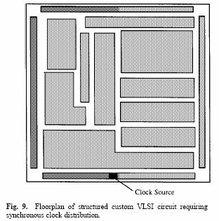
28 Clock Jitter Jitter causes T to vary on a cycle-by-cycle basis In clk R1 t clk T Combinational logic -t jitter +t jitter T T : - 2t jitter t c-q + t plogic + t su so T t c-q + t plogic + t su + 2t jitter Jitter directly reduces the performance of a sequential circuit 28
29 Combined Impact of Skew and Jitter Constraints on the minimum clock period (δ > 0) In D 1 R1 Q t clk1 δ > 0 -t jitter Combinational logic T T + δ 6 12 D R2 Q t clk2 T t c-q + t plogic + t su - δ + 2t jitter t hold t cdlogic + t cdreg δ 2t jitter δ > 0 with jitter: Degrades performance, and makes t hold even harder to meet. (The acceptable skew is reduced by jitter.) 29
30 30
31 Technology scaling Technology scaling, in that long global interconnect lines become much more highly resistive as line dimensions are decreased. This increased line resistance is one of the primary reasons for the growing importance of clock distribution on synchronous performance. 31
32 Clock distribution strategies (only relative phase between two clocking element is important) 32
33 Achieve Zero skew routing Route clock to destinations such that clock edges appear at the same time 33
34 Clock tree Single driver---if the interconnect resistance of the buffer at the clock source is small as compared to the buffer output resistance, maintaining high-quality waveform shapes (i.e., short transition times) Use elmore formula to compute delay Balance delay paths Drawback---large delay, drive capability should be high 34
35 Terminology The unique clock source is frequently described as the root of the tree, the initial portion of the tree as the trunk, individual paths driving each register as the branches, and the registers being driven as the leaves 35
36 Buffered clock Tree interconnect resistance large The most common and general approach to equi-potential clock distribution is the use of buffered trees, It leads to an asymmetric structure ALL PATHS ARE BALANCED 36
37 37
38 38
39 Buffered clock Tree Insert buffers either at the clock source and/or along a clock path, forming a tree structure. 39
40 Buffers The distributed buffers serve the double function of amplifying the clock signals degraded by the distributed interconnect impedances and isolating the local clock nets from upstream load impedances 40
41 DESIGN All nodes have capacitance All branches have resistance Fix the load (fan out ) of each buffer Compute no.of levels required Position the buffers optimally Guidelines- minimize delay buffer delay=segment delay 41
42 42
43 3D Skew Visualization 43
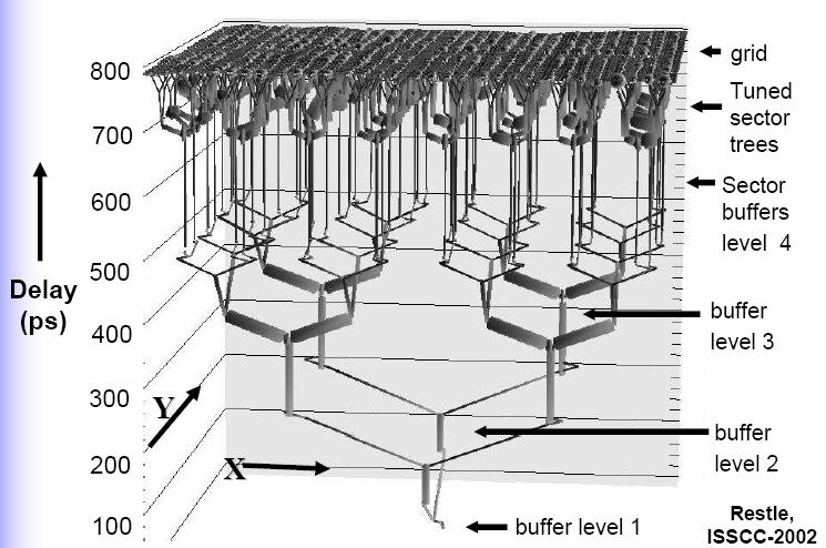
44 Mesh version of clk tree 44
45 Mesh version of clock tree Shunt paths further down the clock distribution network are placed to minimize the interconnect resistance within the clock tree. This mesh structure effectively places the branch resistances in parallel, minimizing the clock skew. 45
46 46
47 CDN properties H TREE symmetric,regular array, clk skew can be small X TREE- variant of H TREE Zero skew is achieved maintaining the distributed interconnect and buffers to be identical from the clock signal source to the clocked register of each clock path. each clock path from the clock source to a clocked register has practically the same delay. 47
48 Skew The primary delay difference between the clock signal paths is due to variations in process parameters that affect the interconnect impedance and, in particular, any active distributed buffer amplifiers. The amount of clock skew within an H-tree structured clock distribution network is strongly dependent upon the physical size, the control of the semiconductor process, and the degree to which active buffers are distributed within the H- 48 tree structure
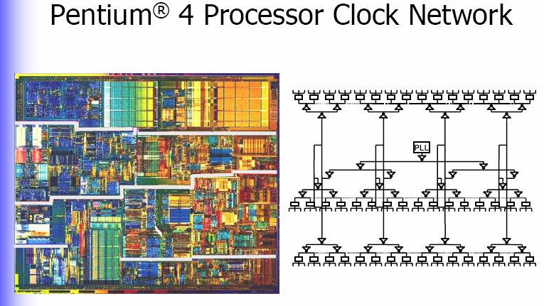
49 Clock Distribution H-tree CLK Clock is distributed in a tree-like fashion 49
50 H-Tree Clock Network If the paths are perfectly balanced, clock skew is zero Clock Can insert clock gating at multiple levels in clock tree Can shut off entire subtree if all gating conditions are satisfied Idle condition Clock Gated clock 50
51 More realistic H-tree [Restle98] 51
52 Tapered H tree The conductor widths in H-tree structures are designed to progressively decrease as the signal propagates to lower levels of the hierarchy. This strategy minimizes reflections of the high-speed clock signals at the branching points. 52
53 H Tree---Difficulty -1 Clock routed in both the vertical and horizontal directions. For a standard twolevel metal CMOS process, this manhattan structure creates added difficulty in routing the clock lines without using either resistive interconnect or multiple high resistance vias between the two metal lines. 3 level metal process 53
54 Difficulty -2 Furthermore, the interconnect capacitance (and therefore the power dissipation) is much greater for the H-tree as compared with the standard clock tree since the total wire length tends to be much greater An important tradeoff between clock delay and clock skew in the design of highspeed clock distribution networks. 54
55 Grid Low skew achievable Lots of excess interconnect Large power dissipation 55
56 Clock distribution-hierarchical Distribute global reference to various parts of the chip with zero skew Local distribution of the clock while considering local load variations., permitted clk skew,. Power saving strategies are used here. 56
57 GCLK Gridded global clock signal (GCLK) is distributed over the entire IC in order to maintain a low-resistance reference clock signal and to distribute the power dissipated by the clock distribution network across the die area The global clock signal GCLK is the source of thousands of buffered and conditional (or gated) clock signals driving registers across the IC 57
58 58
59 Example: DEC Alpha Clock Frequency: 300 MHz Million Transistors Total Clock Load: 3.75 nf Power in Clock Distribution network : 20 W (out of 50) Uses Two Level Clock Distribution: Single 6-stage driver at center of chip Secondary buffers drive left and right side clock grid in Metal3 and Metal4 Total driver size: 58 cm! 59
60 DEC Alpha (EV5) 300 MHz clock (9.3 million transistors on a 16.5x18.1 mm die in 0.5 micron CMOS technology) single phase clock 3.75 nf total clock load Extensive use of dynamic logic 20 W (out of 50) in clock distribution network Two level clock distribution Single 6 stage driver at the center of the chip Secondary buffers drive the left and right sides of the clock grid in m3 and m4 Total equivalent driver size of 58 cm!! 60
61 21164 Clocking t rise = 0.35ns t cycle = 3.3ns Clock waveform final drivers pre-driver Location of clock driver on die t skew = 150ps 2 phase single wire clock, distributed globally 2 distributed driver channels Reduced RC delay/skew Improved thermal distribution 3.75nF clock load 58 cm final driver width Local inverters for latching Conditional clocks in caches to reduce power More complex race checking Device variation 61

62 Clock Drivers 62
63 EV6 (Alpha 21264) Clocking 600 MHz 0.35 micron CMOS t cycle = 1.67ns t rise = 0.35ns Global clock waveform t skew = 50ps PLL 2 Phase, with multiple conditional buffered clocks 2.8 nf clock load 40 cm final driver width Local clocks can be gated off to save power Reduced load/skew Reduced thermal issues Multiple clocks complicate race checking 63
64 21264 Clocking 64
65 PLL ps

66 Clock Skew in Alpha Processor Absolute skew smaller than 90 ps The critical instruction and execution units all see the clock within 65 ps 66


67 ps EV6 Clock Results ps GCLK Skew (at Vdd/2 Crossings) GCLK Rise Times (20% to 80% Extrapolated to 0% to 100%) 67
CMPEN 411 VLSI Digital Circuits Spring 2012 Lecture 17: Dynamic Sequential Circuits And Timing Issues
 CMPEN 411 VLSI Digital Circuits Spring 2012 Lecture 17: Dynamic Sequential Circuits And Timing Issues [Adapted from Rabaey s Digital Integrated Circuits, Second Edition, 2003 J. Rabaey, A. Chandrakasan,
EE115C Winter 2017 Digital Electronic Circuits. Lecture 19: Timing Analysis
 EE115C Winter 2017 Digital Electronic Circuits Lecture 19: Timing Analysis Outline Timing parameters Clock nonidealities (skew and jitter) Impact of Clk skew on timing Impact of Clk jitter on timing Flip-flop-
Xarxes de distribució del senyal de. interferència electromagnètica, consum, soroll de conmutació.
 Xarxes de distribució del senyal de rellotge. Clock skew, jitter, interferència electromagnètica, consum, soroll de conmutació. (transparències generades a partir de la presentació de Jan M. Rabaey, Anantha
The Linear-Feedback Shift Register
 EECS 141 S02 Timing Project 2: A Random Number Generator R R R S 0 S 1 S 2 1 0 0 0 1 0 1 0 1 1 1 0 1 1 1 0 1 1 0 0 1 1 0 0 The Linear-Feedback Shift Register 1 Project Goal Design a 4-bit LFSR SPEED, SPEED,
Lecture 9: Clocking, Clock Skew, Clock Jitter, Clock Distribution and some FM
 Lecture 9: Clocking, Clock Skew, Clock Jitter, Clock Distribution and some FM Mark McDermott Electrical and Computer Engineering The University of Texas at Austin 9/27/18 VLSI-1 Class Notes Why Clocking?
CMPEN 411. Spring Lecture 18: Static Sequential Circuits
 CMPEN 411 VLSI Digital Circuits Spring 2011 Lecture 18: Static Sequential Circuits [Adapted from Rabaey s Digital Integrated Circuits, Second Edition, 2003 J. Rabaey, A. Chandrakasan, B. Nikolic] Sp11
Lecture 25. Dealing with Interconnect and Timing. Digital Integrated Circuits Interconnect
 Lecture 25 Dealing with Interconnect and Timing Administrivia Projects will be graded by next week Project phase 3 will be announced next Tu.» Will be homework-like» Report will be combined poster Today
Lecture 23. Dealing with Interconnect. Impact of Interconnect Parasitics
 Lecture 23 Dealing with Interconnect Impact of Interconnect Parasitics Reduce Reliability Affect Performance Classes of Parasitics Capacitive Resistive Inductive 1 INTERCONNECT Dealing with Capacitance
Timing Issues. Digital Integrated Circuits A Design Perspective. Jan M. Rabaey Anantha Chandrakasan Borivoje Nikolić. January 2003
 Digital Integrated Circuits A Design Perspective Jan M. Rabaey Anantha Chandrakasan Borivoje Nikolić Timing Issues January 2003 1 Synchronous Timing CLK In R Combinational 1 R Logic 2 C in C out Out 2
ΗΜΥ 307 ΨΗΦΙΑΚΑ ΟΛΟΚΛΗΡΩΜΕΝΑ ΚΥΚΛΩΜΑΤΑ Εαρινό Εξάμηνο 2018
 ΗΜΥ 307 ΨΗΦΙΑΚΑ ΟΛΟΚΛΗΡΩΜΕΝΑ ΚΥΚΛΩΜΑΤΑ Εαρινό Εξάμηνο 2018 ΔΙΑΛΕΞΕΙΣ 12-13: esigning ynamic and Static CMOS Sequential Circuits ΧΑΡΗΣ ΘΕΟΧΑΡΙΔΗΣ (ttheocharides@ucy.ac.cy) (ack: Prof. Mary Jane Irwin and
GMU, ECE 680 Physical VLSI Design 1
 ECE680: Physical VLSI Design Chapter VII Timing Issues in Digital Circuits (chapter 10 in textbook) GMU, ECE 680 Physical VLSI Design 1 Synchronous Timing (Fig. 10 1) CLK In R Combinational 1 R Logic 2
Lecture 9: Sequential Logic Circuits. Reading: CH 7
 Lecture 9: Sequential Logic Circuits Reading: CH 7 Sequential Logic FSM (Finite-state machine) Inputs Current State COMBINATIONAL LOGIC Registers Outputs = f(current, inputs) Next state 2 storage mechanisms
Topics. Dynamic CMOS Sequential Design Memory and Control. John A. Chandy Dept. of Electrical and Computer Engineering University of Connecticut
 Topics Dynamic CMOS Sequential Design Memory and Control Dynamic CMOS In static circuits at every point in time (except when switching) the output is connected to either GND or V DD via a low resistance
MODULE 5 Chapter 7. Clocked Storage Elements
 MODULE 5 Chapter 7 Clocked Storage Elements 3/9/2015 1 Outline Background Clocked Storage Elements Timing, terminology, classification Static CSEs Latches Registers Dynamic CSEs Latches Registers 3/9/2015
Integrated Circuits & Systems
 Federal University of Santa Catarina Center for Technology Computer Science & Electronics Engineering Integrated Circuits & Systems INE 5442 Lecture 18 CMOS Sequential Circuits - 1 guntzel@inf.ufsc.br
Luis Manuel Santana Gallego 31 Investigation and simulation of the clock skew in modern integrated circuits
 Luis Manuel Santana Gallego 31 Investigation and simulation of the clock skew in modern egrated circuits 3. Clock skew 3.1. Definitions For two sequentially adjacent registers, as shown in figure.1, C
Digital Integrated Circuits A Design Perspective
 Digital Integrated Circuits A Design Perspective Jan M. Rabaey Anantha Chandrakasan Borivoje Nikolic Designing Sequential Logic Circuits November 2002 Sequential Logic Inputs Current State COMBINATIONAL
ESE 570: Digital Integrated Circuits and VLSI Fundamentals
 ESE 570: Digital Integrated Circuits and VLSI Fundamentals Lec 19: March 29, 2018 Memory Overview, Memory Core Cells Today! Charge Leakage/Charge Sharing " Domino Logic Design Considerations! Logic Comparisons!
! Charge Leakage/Charge Sharing. " Domino Logic Design Considerations. ! Logic Comparisons. ! Memory. " Classification. " ROM Memories.
 ESE 57: Digital Integrated Circuits and VLSI Fundamentals Lec 9: March 9, 8 Memory Overview, Memory Core Cells Today! Charge Leakage/ " Domino Logic Design Considerations! Logic Comparisons! Memory " Classification
CSE241 VLSI Digital Circuits Winter Lecture 07: Timing II
 CSE241 VLSI Digital Circuits Winter 2003 Lecture 07: Timing II CSE241 L3 ASICs.1 Delay Calculation Cell Fall Cap\Tr 0.05 0.2 0.5 0.01 0.02 0.16 0.30 0.5 2.0 0.04 0.32 0.178 0.08 0.64 0.60 1.20 0.1ns 0.147ns
CMOS Inverter. Performance Scaling
 Announcements Exam #2 regrade requests due today. Homework #8 due today. Final Exam: Th June 12, 8:30 10:20am, CMU 120 (extension to 11:20am requested). Grades available for viewing via Catalyst. CMOS
ESE 570: Digital Integrated Circuits and VLSI Fundamentals
 ESE 570: Digital Integrated Circuits and VLSI Fundamentals Lec 18: March 27, 2018 Dynamic Logic, Charge Injection Lecture Outline! Sequential MOS Logic " D-Latch " Timing Constraints! Dynamic Logic " Domino
Issues on Timing and Clocking
 ECE152B TC 1 Issues on Timing and Clocking X Combinational Logic Z... clock clock clock period ECE152B TC 2 Latch and Flip-Flop L CK CK 1 L1 1 L2 2 CK CK CK ECE152B TC 3 Clocking X Combinational Logic...
GMU, ECE 680 Physical VLSI Design
 ECE680: Physical VLSI esign Chapter IV esigning Sequential Logic Circuits (Chapter 7) 1 Sequential Logic Inputs Current State COMBINATIONAL LOGIC Registers Outputs Next state 2 storage mechanisms positive
Lecture 21: Packaging, Power, & Clock
 Lecture 21: Packaging, Power, & Clock Outline Packaging Power Distribution Clock Distribution 2 Packages Package functions Electrical connection of signals and power from chip to board Little delay or
Clock Strategy. VLSI System Design NCKUEE-KJLEE
 Clock Strategy Clocked Systems Latch and Flip-flops System timing Clock skew High speed latch design Phase locked loop ynamic logic Multiple phase Clock distribution Clocked Systems Most VLSI systems are
Chapter 13. Clocked Circuits SEQUENTIAL VS. COMBINATIONAL CMOS TG LATCHES, FLIP FLOPS. Baker Ch. 13 Clocked Circuits. Introduction to VLSI
 Chapter 13 Clocked Circuits SEQUENTIAL VS. COMBINATIONAL CMOS TG LATCHES, FLIP FLOPS SET-RESET (SR) ARBITER LATCHES FLIP FLOPS EDGE TRIGGERED DFF FF TIMING Joseph A. Elias, Ph.D. Adjunct Professor, University
CARNEGIE MELLON UNIVERSITY DEPARTMENT OF ELECTRICAL AND COMPUTER ENGINEERING DIGITAL INTEGRATED CIRCUITS FALL 2002
 CARNEGIE MELLON UNIVERSITY DEPARTMENT OF ELECTRICAL AND COMPUTER ENGINEERING 18-322 DIGITAL INTEGRATED CIRCUITS FALL 2002 Final Examination, Monday Dec. 16, 2002 NAME: SECTION: Time: 180 minutes Closed
Clocking Issues: Distribution, Energy
 EE M216A.:. Fall 2010 Lecture 12 Clocking Issues: istribution, Energy Prof. ejan Marković ee216a@gmail.com Clock istribution Goals: eliver clock to all memory elements with acceptable skew eliver clock
9/18/2008 GMU, ECE 680 Physical VLSI Design
 ECE680: Physical VLSI esign Chapter IV esigning Sequential Logic Circuits (Chapter 7) 1 Sequential Logic Inputs Current State COMBINATIONAL LOGIC Registers Outputs Next state 2 storage mechanisms positive
Digital Integrated Circuits A Design Perspective
 igital Integrated Circuits A esign Perspective Jan M. Rabaey Anantha Chandrakasan Borivoje Nikolic esigning Sequential Logic Circuits November 2002 Sequential Logic Inputs Current State COMBINATIONAL LOGIC
EEC 216 Lecture #3: Power Estimation, Interconnect, & Architecture. Rajeevan Amirtharajah University of California, Davis
 EEC 216 Lecture #3: Power Estimation, Interconnect, & Architecture Rajeevan Amirtharajah University of California, Davis Outline Announcements Review: PDP, EDP, Intersignal Correlations, Glitching, Top
Digital Integrated Circuits A Design Perspective. Semiconductor. Memories. Memories
 Digital Integrated Circuits A Design Perspective Semiconductor Chapter Overview Memory Classification Memory Architectures The Memory Core Periphery Reliability Case Studies Semiconductor Memory Classification
Digital Integrated Circuits A Design Perspective
 igital Integrated Circuits A esign Perspective Jan M. Rabaey Anantha Chandrakasan Borivoje Nikolic esigning Sequential Logic Circuits November 2002 Naming Conventions In our text: a latch is level sensitive
Jan M. Rabaey Anantha Chandrakasan Borivoje Nikolic. November Digital Integrated Circuits 2nd Sequential Circuits
 igital Integrated Circuits A esign Perspective Jan M. Rabaey Anantha Chandrakasan Borivoje Nikolic esigning i Sequential Logic Circuits November 2002 Sequential Logic Inputs Current State COMBINATIONAL
Topics. CMOS Design Multi-input delay analysis. John A. Chandy Dept. of Electrical and Computer Engineering University of Connecticut
 Topics CMO Design Multi-input delay analysis pring 25 Transmission Gate OUT Z OUT Z pring 25 Transmission Gate OUT When is low, the output is at high impedance When is high, the output follows However,
Semiconductor Memories
 Semiconductor References: Adapted from: Digital Integrated Circuits: A Design Perspective, J. Rabaey UCB Principles of CMOS VLSI Design: A Systems Perspective, 2nd Ed., N. H. E. Weste and K. Eshraghian
EE141- Spring 2007 Digital Integrated Circuits
 EE141- Spring 27 igital Integrated Circuits Lecture 19 Sequential Circuits 1 Administrative Stuff Project Ph. 2 due Tu. 5pm 24 Cory box + email ee141- project@bwrc.eecs.berkeley.edu Hw 8 Posts this Fr.,
ESE 570: Digital Integrated Circuits and VLSI Fundamentals
 ESE 570: Digital Integrated Circuits and VLSI Fundamentals Lec 23: April 17, 2018 I/O Circuits, Inductive Noise, CLK Generation Lecture Outline! Packaging! Variation and Testing! I/O Circuits! Inductive
Very Large Scale Integration (VLSI)
") Very Large Scale Integration (VLSI) Lecture 4 Dr. Ahmed H. Madian Ah_madian@hotmail.com Dr. Ahmed H. Madian-VLSI Contents Delay estimation Simple RC model Penfield-Rubenstein Model Logical effort Delay
Very Large Scale Integration (VLSI) Lecture 4 Dr. Ahmed H. Madian Ah_madian@hotmail.com Dr. Ahmed H. Madian-VLSI Contents Delay estimation Simple RC model Penfield-Rubenstein Model Logical effort Delay
Memory, Latches, & Registers
 Memory, Latches, & Registers 1) Structured Logic Arrays 2) Memory Arrays 3) Transparent Latches 4) How to save a few bucks at toll booths 5) Edge-triggered Registers L13 Memory 1 General Table Lookup Synthesis
Lecture 27: Latches. Final presentations May 8, 1-5pm, BWRC Final reports due May 7 Final exam, Monday, May :30pm, 241 Cory
 EE241 - Spring 2008 Advanced Digital Integrated Circuits Lecture 27: Latches Timing Announcements Wrapping-up the class: Final presentations May 8, 1-5pm, BWRC Final reports due May 7 Final exam, Monday,
VLSI Design, Fall Logical Effort. Jacob Abraham
 6. Logical Effort 6. Logical Effort Jacob Abraham Department of Electrical and Computer Engineering The University of Texas at Austin VLSI Design Fall 207 September 20, 207 ECE Department, University of
Digital Integrated Circuits A Design Perspective
 Semiconductor Memories Adapted from Chapter 12 of Digital Integrated Circuits A Design Perspective Jan M. Rabaey et al. Copyright 2003 Prentice Hall/Pearson Outline Memory Classification Memory Architectures
Y. Tsiatouhas. VLSI Systems and Computer Architecture Lab
 CMOS INTEGRATE CIRCUIT ESIGN TECHNIUES University of Ioannina Memory Elements and other Circuits ept. of Computer Science and Engineering Y. Tsiatouhas CMOS Integrated Circuit esign Techniques Overview.
Name: Answers. Mean: 83, Standard Deviation: 12 Q1 Q2 Q3 Q4 Q5 Q6 Total. ESE370 Fall 2015
 University of Pennsylvania Department of Electrical and System Engineering Circuit-Level Modeling, Design, and Optimization for Digital Systems ESE370, Fall 2015 Final Tuesday, December 15 Problem weightings
UMBC. At the system level, DFT includes boundary scan and analog test bus. The DFT techniques discussed focus on improving testability of SAFs.
 Overview Design for testability(dft) makes it possible to: Assure the detection of all faults in a circuit. Reduce the cost and time associated with test development. Reduce the execution time of performing
5. Sequential Logic x Computation Structures Part 1 Digital Circuits. Copyright 2015 MIT EECS
 5. Sequential Logic 6.004x Computation Structures Part 1 igital Circuits Copyright 2015 MIT EECS 6.004 Computation Structures L5: Sequential Logic, Slide #1 Something We Can t Build (Yet) What if you were
Chapter Overview. Memory Classification. Memory Architectures. The Memory Core. Periphery. Reliability. Memory
 SRAM Design Chapter Overview Classification Architectures The Core Periphery Reliability Semiconductor Classification RWM NVRWM ROM Random Access Non-Random Access EPROM E 2 PROM Mask-Programmed Programmable
ESE 570: Digital Integrated Circuits and VLSI Fundamentals
 ESE 570: Digital Integrated Circuits and VLSI Fundamentals Lec 24: April 19, 2018 Crosstalk and Wiring, Transmission Lines Lecture Outline! Crosstalk! Repeaters in Wiring! Transmission Lines " Where transmission
EE141Microelettronica. CMOS Logic
 Microelettronica CMOS Logic CMOS logic Power consumption in CMOS logic gates Where Does Power Go in CMOS? Dynamic Power Consumption Charging and Discharging Capacitors Short Circuit Currents Short Circuit
Designing Sequential Logic Circuits
 igital Integrated Circuits (83-313) Lecture 5: esigning Sequential Logic Circuits Semester B, 2016-17 Lecturer: r. Adam Teman TAs: Itamar Levi, Robert Giterman 26 April 2017 isclaimer: This course was
ECEN 248: INTRODUCTION TO DIGITAL SYSTEMS DESIGN. Week 9 Dr. Srinivas Shakkottai Dept. of Electrical and Computer Engineering
 ECEN 248: INTRODUCTION TO DIGITAL SYSTEMS DESIGN Week 9 Dr. Srinivas Shakkottai Dept. of Electrical and Computer Engineering TIMING ANALYSIS Overview Circuits do not respond instantaneously to input changes
! Crosstalk. ! Repeaters in Wiring. ! Transmission Lines. " Where transmission lines arise? " Lossless Transmission Line.
 ESE 570: Digital Integrated Circuits and VLSI Fundamentals Lec 24: April 19, 2018 Crosstalk and Wiring, Transmission Lines Lecture Outline! Crosstalk! Repeaters in Wiring! Transmission Lines " Where transmission
9/18/2008 GMU, ECE 680 Physical VLSI Design
 ECE680: Physical VLSI Design Chapter III CMOS Device, Inverter, Combinational circuit Logic and Layout Part 3 Combinational Logic Gates (textbook chapter 6) 9/18/2008 GMU, ECE 680 Physical VLSI Design
EE 447 VLSI Design. Lecture 5: Logical Effort
 EE 447 VLSI Design Lecture 5: Logical Effort Outline Introduction Delay in a Logic Gate Multistage Logic Networks Choosing the Best Number of Stages Example Summary EE 4475: VLSI Logical Design Effort
Sequential vs. Combinational
 Sequential Circuits Sequential vs. Combinational Combinational Logic: Output depends only on current input TV channel selector (-9) inputs system outputs Sequential Logic: Output depends not only on current
L4: Sequential Building Blocks (Flip-flops, Latches and Registers)
") L4: Sequential Building Blocks (Flip-flops, Latches and Registers) Acknowledgements:., Materials in this lecture are courtesy of the following people and used with permission. - Randy H. Katz (University
L4: Sequential Building Blocks (Flip-flops, Latches and Registers) Acknowledgements:., Materials in this lecture are courtesy of the following people and used with permission. - Randy H. Katz (University
LOGIC CIRCUITS. Basic Experiment and Design of Electronics. Ho Kyung Kim, Ph.D.
 Basic Experiment and Design of Electronics LOGIC CIRCUITS Ho Kyung Kim, Ph.D. hokyung@pusan.ac.kr School of Mechanical Engineering Pusan National University Digital IC packages TTL (transistor-transistor
Lecture 6: Logical Effort
 Lecture 6: Logical Effort Outline Logical Effort Delay in a Logic Gate Multistage Logic Networks Choosing the Best Number of Stages Example Summary Introduction Chip designers face a bewildering array
Logical Effort: Designing for Speed on the Back of an Envelope David Harris Harvey Mudd College Claremont, CA
 Logical Effort: Designing for Speed on the Back of an Envelope David Harris David_Harris@hmc.edu Harvey Mudd College Claremont, CA Outline o Introduction o Delay in a Logic Gate o Multi-stage Logic Networks
Topic 8: Sequential Circuits
 Topic 8: Sequential Circuits Readings : Patterson & Hennesy, Appendix B.4 - B.6 Goals Basic Principles behind Memory Elements Clocks Applications of sequential circuits Introduction to the concept of the
ESE 570: Digital Integrated Circuits and VLSI Fundamentals
 ESE 570: Digital Integrated Circuits and VLSI Fundamentals Lec 21: April 4, 2017 Memory Overview, Memory Core Cells Penn ESE 570 Spring 2017 Khanna Today! Memory " Classification " ROM Memories " RAM Memory
EE141-Fall 2011 Digital Integrated Circuits
 EE4-Fall 20 Digital Integrated Circuits Lecture 5 Memory decoders Administrative Stuff Homework #6 due today Project posted Phase due next Friday Project done in pairs 2 Last Lecture Last lecture Logical
EE241 - Spring 2006 Advanced Digital Integrated Circuits
 EE241 - Spring 2006 Advanced Digital Integrated Circuits Lecture 20: Asynchronous & Synchronization Self-timed and Asynchronous Design Functions of clock in synchronous design 1) Acts as completion signal
Lecture 8: Combinational Circuit Design
 Lecture 8: Combinational Circuit Design Mark McDermott Electrical and Computer Engineering The University of Texas at ustin 9/5/8 Verilog to Gates module mux(input s, d0, d, output y); assign y = s? d
Chapter 5 CMOS Logic Gate Design
 Chapter 5 CMOS Logic Gate Design Section 5. -To achieve correct operation of integrated logic gates, we need to satisfy 1. Functional specification. Temporal (timing) constraint. (1) In CMOS, incorrect
Fault Modeling. 李昆忠 Kuen-Jong Lee. Dept. of Electrical Engineering National Cheng-Kung University Tainan, Taiwan. VLSI Testing Class
 Fault Modeling 李昆忠 Kuen-Jong Lee Dept. of Electrical Engineering National Cheng-Kung University Tainan, Taiwan Class Fault Modeling Some Definitions Why Modeling Faults Various Fault Models Fault Detection
Chapter 7. Sequential Circuits Registers, Counters, RAM
 Chapter 7. Sequential Circuits Registers, Counters, RAM Register - a group of binary storage elements suitable for holding binary info A group of FFs constitutes a register Commonly used as temporary storage
Semiconductor memories
 Semiconductor memories Semiconductor Memories Data in Write Memory cell Read Data out Some design issues : How many cells? Function? Power consuption? Access type? How fast are read/write operations? Semiconductor
Itanium TM Processor Clock Design
 Itanium TM Processor Design Utpal Desai 1, Simon Tam, Robert Kim, Ji Zhang, Stefan Rusu Intel Corporation, M/S SC12-502, 2200 Mission College Blvd, Santa Clara, CA 95052 ABSTRACT The Itanium processor
EECS 427 Lecture 14: Timing Readings: EECS 427 F09 Lecture Reminders
 EECS 427 Lecture 14: Timing Readings: 10.1-10.3 EECS 427 F09 Lecture 14 1 Reminders CA assignments Please submit CA6 by tomorrow noon CA7 is due in a week Seminar by Prof. Bora Nikolic SRAM variability
Hold Time Illustrations
 Hold Time Illustrations EE213-L09-Sequential Logic.1 Pingqiang, ShanghaiTech, 2018 Hold Time Illustrations EE213-L09-Sequential Logic.2 Pingqiang, ShanghaiTech, 2018 Hold Time Illustrations EE213-L09-Sequential
Implementation of Clock Network Based on Clock Mesh
 International Conference on Information Technology and Management Innovation (ICITMI 2015) Implementation of Clock Network Based on Clock Mesh He Xin 1, a *, Huang Xu 2,b and Li Yujing 3,c 1 Sichuan Institute
MOSIS REPORT. Spring MOSIS Report 1. MOSIS Report 2. MOSIS Report 3
 MOSIS REPORT Spring 2010 MOSIS Report 1 MOSIS Report 2 MOSIS Report 3 MOSIS Report 1 Design of 4-bit counter using J-K flip flop I. Objective The purpose of this project is to design one 4-bit counter
ECE429 Introduction to VLSI Design
 ECE429 Introduction to VLSI Design Lecture 5: LOGICAL EFFORT Erdal Oruklu Illinois Institute of Technology Some of these slides have been adapted from the slides provided by David Harris, Harvey Mudd College
MODULE III PHYSICAL DESIGN ISSUES
 VLSI Digital Design MODULE III PHYSICAL DESIGN ISSUES 3.2 Power-supply and clock distribution EE - VDD -P2006 3:1 3.1.1 Power dissipation in CMOS gates Power dissipation importance Package Cost. Power
EE241 - Spring 2007 Advanced Digital Integrated Circuits. Announcements
 EE241 - Spring 2007 Advanced Digital Integrated Circuits Lecture 25: Synchronization Timing Announcements Homework 5 due on 4/26 Final exam on May 8 in class Project presentations on May 3, 1-5pm 2 1 Project
Next, we check the race condition to see if the circuit will work properly. Note that the minimum logic delay is a single sum.
 UNIVERSITY OF CALIFORNIA College of Engineering Department of Electrical Engineering and Computer Sciences Last modified on May 1, 2003 by Dejan Markovic (dejan@eecs.berkeley.edu) Prof. Jan Rabaey EECS
LOGIC CIRCUITS. Basic Experiment and Design of Electronics
 Basic Experiment and Design of Electronics LOGIC CIRCUITS Ho Kyung Kim, Ph.D. hokyung@pusan.ac.kr School of Mechanical Engineering Pusan National University Outline Combinational logic circuits Output
Static CMOS Circuits. Example 1
 Static CMOS Circuits Conventional (ratio-less) static CMOS Covered so far Ratio-ed logic (depletion load, pseudo nmos) Pass transistor logic ECE 261 Krish Chakrabarty 1 Example 1 module mux(input s, d0,
EECS 151/251A Homework 5
 EECS 151/251A Homework 5 Due Monday, March 5 th, 2018 Problem 1: Timing The data-path shown below is used in a simple processor. clk rd1 rd2 0 wr regfile 1 0 ALU REG 1 The elements used in the design have
NTE74HC299 Integrated Circuit TTL High Speed CMOS, 8 Bit Universal Shift Register with 3 State Output
 NTE74HC299 Integrated Circuit TTL High Speed CMOS, 8 Bit Universal Shift Register with 3 State Output Description: The NTE74HC299 is an 8 bit shift/storage register with three state bus interface capability
UNIVERSITY OF CALIFORNIA, BERKELEY College of Engineering Department of Electrical Engineering and Computer Sciences
 UNIVERSITY OF CALIFORNIA, BERKELEY College of Engineering Department of Electrical Engineering and Computer Sciences Elad Alon Homework #9 EECS141 PROBLEM 1: TIMING Consider the simple state machine shown
Managing Physical Design Issues in ASIC Toolflows Complex Digital Systems Christopher Batten February 21, 2006
 Managing Physical Design Issues in ASI Toolflows 6.375 omplex Digital Systems hristopher Batten February 1, 006 Managing Physical Design Issues in ASI Toolflows Logical Effort Physical Design Issues lock
Digital System Clocking: High-Performance and Low-Power Aspects. Vojin G. Oklobdzija, Vladimir M. Stojanovic, Dejan M. Markovic, Nikola M.
 Digital System Clocking: High-Performance and Low-Power Aspects Vojin G. Oklobdzija, Vladimir M. Stojanovic, Dejan M. Markovic, Nikola M. Nedovic Wiley-Interscience and IEEE Press, January 2003 Nov. 14,
CMOS Digital Integrated Circuits Lec 13 Semiconductor Memories
 Lec 13 Semiconductor Memories 1 Semiconductor Memory Types Semiconductor Memories Read/Write (R/W) Memory or Random Access Memory (RAM) Read-Only Memory (ROM) Dynamic RAM (DRAM) Static RAM (SRAM) 1. Mask
ALU A functional unit
 ALU A functional unit that performs arithmetic operations such as ADD, SUB, MPY logical operations such as AND, OR, XOR, NOT on given data types: 8-,16-,32-, or 64-bit values A n-1 A n-2... A 1 A 0 B n-1
Problems in VLSI design
 Problems in VLSI design wire and transistor sizing signal delay in RC circuits transistor and wire sizing Elmore delay minimization via GP dominant time constant minimization via SDP placement problems
C.K. Ken Yang UCLA Courtesy of MAH EE 215B
 Decoders: Logical Effort Applied C.K. Ken Yang UCLA yang@ee.ucla.edu Courtesy of MAH 1 Overview Reading Rabaey 6.2.2 (Ratio-ed logic) W&H 6.2.2 Overview We have now gone through the basics of decoders,
L4: Sequential Building Blocks (Flip-flops, Latches and Registers)
") L4: Sequential Building Blocks (Flip-flops, Latches and Registers) Acknowledgements: Lecture material adapted from R. Katz, G. Borriello, Contemporary Logic esign (second edition), Prentice-Hall/Pearson
L4: Sequential Building Blocks (Flip-flops, Latches and Registers) Acknowledgements: Lecture material adapted from R. Katz, G. Borriello, Contemporary Logic esign (second edition), Prentice-Hall/Pearson
Physical Design of Digital Integrated Circuits (EN0291 S40) Sherief Reda Division of Engineering, Brown University Fall 2006
 Sherief Reda Division of Engineering, Brown University Fall 2006") Physical Design of Digital Integrated Circuits (EN0291 S40) Sherief Reda Division of Engineering, Brown University Fall 2006 1 Lecture 04: Timing Analysis Static timing analysis STA for sequential circuits
Physical Design of Digital Integrated Circuits (EN0291 S40) Sherief Reda Division of Engineering, Brown University Fall 2006 1 Lecture 04: Timing Analysis Static timing analysis STA for sequential circuits
EE382 Processor Design Winter 1999 Chapter 2 Lectures Clocking and Pipelining
 Slide 1 EE382 Processor Design Winter 1999 Chapter 2 Lectures Clocking and Pipelining Slide 2 Topics Clocking Clock Parameters Latch Types Requirements for reliable clocking Pipelining Optimal pipelining
CMOS logic gates. João Canas Ferreira. March University of Porto Faculty of Engineering
 CMOS logic gates João Canas Ferreira University of Porto Faculty of Engineering March 2016 Topics 1 General structure 2 General properties 3 Cell layout João Canas Ferreira (FEUP) CMOS logic gates March
Spiral 2 7. Capacitance, Delay and Sizing. Mark Redekopp
 2-7.1 Spiral 2 7 Capacitance, Delay and Sizing Mark Redekopp 2-7.2 Learning Outcomes I understand the sources of capacitance in CMOS circuits I understand how delay scales with resistance, capacitance
ALU, Latches and Flip-Flops
 CSE14: Components and Design Techniques for Digital Systems ALU, Latches and Flip-Flops Tajana Simunic Rosing Where we are. Last time: ALUs Plan for today: ALU example, latches and flip flops Exam #1 grades
Adders, subtractors comparators, multipliers and other ALU elements
 CSE4: Components and Design Techniques for Digital Systems Adders, subtractors comparators, multipliers and other ALU elements Adders 2 Circuit Delay Transistors have instrinsic resistance and capacitance
Introduction to Computer Engineering. CS/ECE 252, Fall 2012 Prof. Guri Sohi Computer Sciences Department University of Wisconsin Madison
 Introduction to Computer Engineering CS/ECE 252, Fall 2012 Prof. Guri Sohi Computer Sciences Department University of Wisconsin Madison Chapter 3 Digital Logic Structures Slides based on set prepared by
Skew-Tolerant Circuit Design
 Skew-Tolerant Circuit Design David Harris David_Harris@hmc.edu December, 2000 Harvey Mudd College Claremont, CA Outline Introduction Skew-Tolerant Circuits Traditional Domino Circuits Skew-Tolerant Domino
ESE570 Spring University of Pennsylvania Department of Electrical and System Engineering Digital Integrated Cicruits AND VLSI Fundamentals
 University of Pennsylvania Department of Electrical and System Engineering Digital Integrated Cicruits AND VLSI Fundamentals ESE570, Spring 017 Final Wednesday, May 3 4 Problems with point weightings shown.