Solution 11:00 AM, Wednesday February 10, 2010, 108 Nedderman Hall 80 minutes allowed (last four digits of your student #) ( if new)
|
|
|
- Derick Sharp
- 5 years ago
- Views:
Transcription
1 MidTerm - EE 5342 (print last name) (print first name) Solution 11:00 AM, Wednesday February 10, 2010, 108 Nedderman Hall 80 minutes allowed (last four digits of your student #) ( if new) Instructions: 1. Do your own work. 2. You may use a legal copy of the Massobrio and Antognetti text, you may write notes in your text, and 1 page of additional notes. You may NOT pass a book or note sheet to another student. 3. Calculator allowed. You may NOT share a calculator with another student. 4. Where values or equations are given on this cover sheet, use them in lieu of any other source. If a value is not given, explicitly state definitions and assumptions that you use. 5. Where necessary, calculate parameters if they cannot be read from a graph. 6. Do all work in the spaces provided on this exam paper. If you write on the back of a sheet, make the notation "PTO" in your solution in order to assure that material written on the back of the page is evaluated for a grade. AN EXTRA BLANK SHEET IS ATTACHED AT THE BACK OF THE EXAM. 7. Show all calculations, making numerical substitutions and giving numerical results where possible. 8. Write answers in space given. 9. Unless stated otherwise, T = 300K, V t = mv (to agree with M&K k and q values) 10. Unless otherwise stated, the material is silicon (300K) with n i = 1.45E10 cm -3 N c = 2.8E19 cm -3 qχ Si = 4.05 ev E g,si = ev. N v = 1.04E19 cm For the work function of poly silicon, use φ n+ = χ si = 4.05 V φ p+ = χ Si + E g,si /q = V. 12. For minority carrier (either electrons or holes) lifetime in silicon, use the relationship τ min = (4.5E-5 sec)/(1 + N i /1E17 + (N i /5E17) 2 ), where N i = the total impurity concentration in cm For holes in silicon doped primarily with boron, assume μ p = {470.5 [1+(N i 2.23E17) ]}+44.9, in cm 2 /V-sec. 14. For electrons in silicon doped primarily with phosphorous, assume μ n = {1414 [1+(N i 9.2E16) ]}+68.5, in cm 2 /V-sec. 15. For electrons in silicon doped primarily with arsenic, assume μ n = {1417 [1+(N i 9.68E16) ]}+52.2, in cm 2 /V-sec. (In 12 through 16, N i = the total impurity concentration in n- or p-type material, compensated or not). 16. Metal gate work functions should be assumed to be φ M,Al = 4.1 V for aluminum, φ M,Pt = 5.3 V for platinum, φ M,Au = 4.75 V for gold 17. The electron affinity of SiO 2 is χ SiO2 = 0.95 V. 18. Planck constant h = 6.625E-34 J-s = 4.135E-15 ev-s, (1 ev = 1.602E-19 Joule). 19. free electron mass m o = 9.11E-28 g. 20. Boltzmann constant, k = 1.38E-23 J/K 21. Electron charge, q = 1.602E-19 Coulomb 22. Permittivity of free space, ε o = 8.854E-14 Fd/cm 23. Relative permittivity of silicon, ε r = Relative permittivity of silicon dioxide, ε rox = The breakdown voltage of an abrupt (step) junction (asymmetrical or one-sided) diode with doping on the lightly doped side of N B is V B = 60(Eg/1.1) 3/2 (10 16 /N B ) 3/4 V. The critical field for breakdown is modeled as E crit = (120V qn B /(ε r ε 0 )) 1/2 (Eg/1.1) 3/4 (10 16 /N B ) 3/8 26. Each part is worth [x] points, as given in the problem. 27. Turn your cell phone off. Page 1
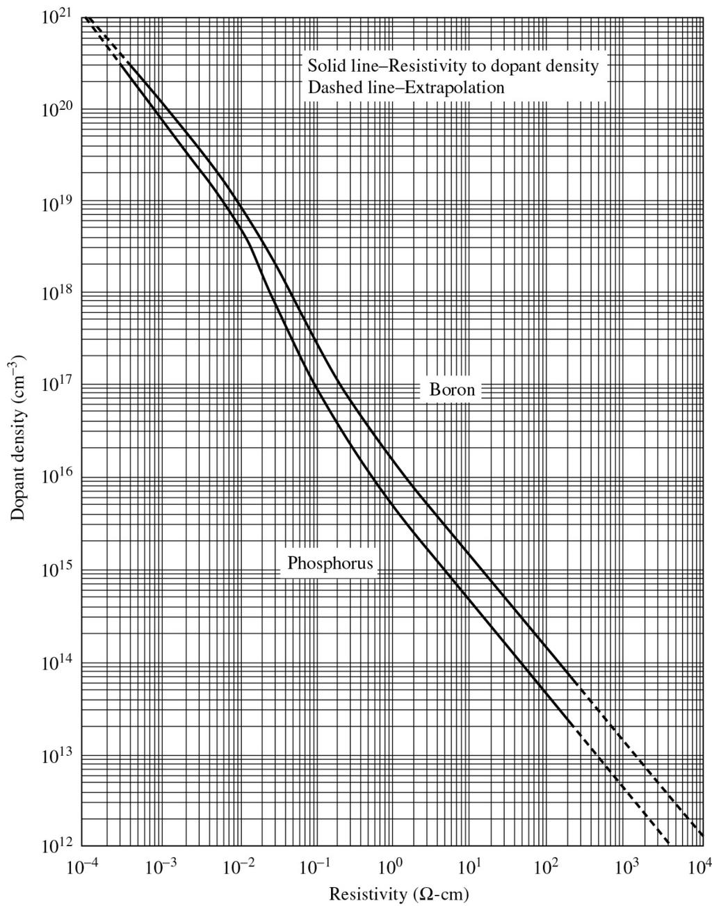
2 Be sure to note the special conditions for statements 12 through 15 after statement 15 on page A region of silicon has 7E15/cm 3 phosphorous and 1E17/cm 3 boron. a. Calculate the majority carrier concentration and type. Na > Nd, so po = -(Nd-Na) = -(7E16/cm3-1E17/cm3) po = 9.3E+16 /cm3 Answer 1a[7] Majority carrier concentration = 9.3E+16 /cm 3, type =. b. Calculate the minority carrier concentration and type. no = ni^2/po no = 2.3E+03 /cm3 Answer 1b[7] Minority carrier concentration = 2.3E+03 /cm 3, type =. c. What is the majority carrier mobility. The net impurity concentration is Na+Nd = 1.07E+17 /cm3 So from the chart, MUp = 310 cm2/v-sec Answer 1c[7] Majority carrier mobility = 310 cm 2 /V-sec. d. What is the minority carrier diffusion coefficient. The net impurity concentration is Na+Nd = 1.07E17/cm3, so from the chart Dn = 18 cm2/sec Answer 1d[7] Minority carrier diffusion coefficient = 18 cm 2 /sec. e. This material is made into a diode with the doping on the other side being 4E15/cm 3. What is the contact potential of this diode? Vbi = Vt*ln(Na*Nd/ni^2) Vbi = V Answer 1e[8] Contact potential = V. f. What is the capacitance per unit area for this diode when the applied voltage is zero volts? From the chart, for N- = 4E15/cm3, and Vbi-Va = 700 mv C'jo = 22.5 nf/cm2 Answer 1f[8] Capacitance per unit area = 21 n Fd/cm. Page 2
3 2. A region of silicon has n = 2E17/cm 3 and a majority carrier mobility of 550 cm 2 /V-sec, and a minority carrier mobility of 250 cm 2 /V-sec. Assume that the total impurity concentration is 2.8E17/cm 3. a. What is the minority carrier lifetime in this region? From the chart, for Ni = 2.8E17/cm3 TAUp = 9E-6 sec Answer 2a[8] The minority carrier lifetime is 9E-6 sec. b. What is the minority carrier diffusion length in this region? Lp = (Dp*TAUp) = (250cm2/V-sec* V*9e-6sec) Lp = 7.63E-03 cm Answer 2b[8] The minority carrier diffusion length is 7.63E-03 cm. c. What is the saturation current density for minority current injection into this region from an P+ anode region into the cathode region described above (assume a short diode with charge neutral region width 2 μm)? Is = q*ni^2*dmin/(nd*xcnr) = q*ni^2*mumin*vt/(nd*xcnr) Is = 5.44E-12 A/cm2 Answer 2c[8] The saturation current density is 5.44E-12 A/cm2. d. If the charge neutral region of the cathode region in part c is changed to 500 μm long, what does the saturation current density become? Xcnr will be replaced by Lp*tanh(Xcnr/Lp) = 7.63E-03 cm, so this is a long diode since Lp = 76.3 microns << Xcnr = 500 microns. Is = q*ni^2*dmin/(nd*lmin*tanh(xcnr/lmin) Is = 1.43E-13A/cm2 Answer 2d[8] The saturation current density is 1.43E-13 A/cm2. Page 3
4 3 A diode has a saturation current of 1.2E-14 A. a Evaluate the diode current at 820 mv. id = IS*(exp(vD/Vt)-1) id = A Answer 3a[8] The diode current is 723 ma. b Evaluate the diode conductance at 820 mv. gd = id/(n*vt) gd = 28.0 S Answer 3b[8] The diode conductance is 28E+3 ma/v. c The diode is a n+p diode with p = 3E15/cm 3 in the ( short 2 μm CNR and uncompensated) anode region. What is the diffusion capacitance of this diode at 820 mv. Dn,min = 33.6 cm2/sec from the chart TAUtransit = Wcnr^2/(2*Dmin) TAUtransit = 5.95E-10 sec Cdiff = gd*tau = 1.67E-08 Fd Answer 3c[8] The diffusion capacitance is 1.67E-08 Fd. Page 4
5 Page 5
6 Note: Be sure to recognize that the scale on the left side is φ i - V a = V bi - V a Page 6
7 Figures on pp. 5-7 from Device Electronics for Integrated Circuits, 3/E by Richard S. Muller and Theodore I. Kamins, Copyright 2003 John Wiley & Sons. Inc. Page 7
8 Figures on this page from Physics of Semiconductor Devices, M. Shur, Prentice-Hall, Page 8
p = {470.5 [1+(N i 2.23E17) ]}+44.9, in cm 2 /V-sec. 14. For electrons in silicon doped primarily with phosphorous, assume
![p = {470.5 [1+(N i 2.23E17) ]}+44.9, in cm 2 /V-sec. 14. For electrons in silicon doped primarily with phosphorous, assume](/thumbs/88/117111080.jpg "p = {470.5 [1+(N i 2.23E17) ]}+44.9, in cm 2 /V-sec. 14. For electrons in silicon doped primarily with phosphorous, assume") Final - EE 5340/001 (print last name) (print first name) SOLUTION Wednesday, December 15, 2010, 11:00 AM, 108 Nedderman Hall 2 hr 30 min allowed (last four digits of your student #) (e-mail if new) Instructions:
Final - EE 5340/001 (print last name) (print first name) SOLUTION Wednesday, December 15, 2010, 11:00 AM, 108 Nedderman Hall 2 hr 30 min allowed (last four digits of your student #) (e-mail if new) Instructions:
Quiz #1 Practice Problem Set
 Name: Student Number: ELEC 3908 Physical Electronics Quiz #1 Practice Problem Set? Minutes January 22, 2016 - No aids except a non-programmable calculator - All questions must be answered - All questions
ECEN 3320 Semiconductor Devices Final exam - Sunday December 17, 2000
 Your Name: ECEN 3320 Semiconductor Devices Final exam - Sunday December 17, 2000 1. Review questions a) Illustrate the generation of a photocurrent in a p-n diode by drawing an energy band diagram. Indicate
UNIVERSITY OF CALIFORNIA, BERKELEY College of Engineering Department of Electrical Engineering and Computer Sciences
 UNIVERSITY OF CALIFORNIA, BERKELEY College of Engineering Department of Electrical Engineering and Computer Sciences EE 105: Microelectronic Devices and Circuits Spring 2008 MIDTERM EXAMINATION #1 Time
UNIVERSITY OF CALIFORNIA College of Engineering Department of Electrical Engineering and Computer Sciences. EECS 130 Professor Ali Javey Fall 2006
 UNIVERSITY OF CALIFORNIA College of Engineering Department of Electrical Engineering and Computer Sciences EECS 130 Professor Ali Javey Fall 2006 Midterm I Name: Closed book. One sheet of notes is allowed.
ECE-342 Test 2 Solutions, Nov 4, :00-8:00pm, Closed Book (one page of notes allowed)
") ECE-342 Test 2 Solutions, Nov 4, 2008 6:00-8:00pm, Closed Book (one page of notes allowed) Please use the following physical constants in your calculations: Boltzmann s Constant: Electron Charge: Free
ECE-342 Test 2 Solutions, Nov 4, 2008 6:00-8:00pm, Closed Book (one page of notes allowed) Please use the following physical constants in your calculations: Boltzmann s Constant: Electron Charge: Free
UNIVERSITY OF CALIFORNIA, BERKELEY College of Engineering Department of Electrical Engineering and Computer Sciences
 UNIVERSITY OF CALIFORNIA, BERKELEY College of Engineering Department of Electrical Engineering and Computer Sciences EECS 40 Spring 2000 Introduction to Microelectronic Devices Prof. King MIDTERM EXAMINATION
Semiconductor Physics Problems 2015
 Semiconductor Physics Problems 2015 Page and figure numbers refer to Semiconductor Devices Physics and Technology, 3rd edition, by SM Sze and M-K Lee 1. The purest semiconductor crystals it is possible
UNIVERSITY OF CALIFORNIA College of Engineering Department of Electrical Engineering and Computer Sciences. EECS 130 Professor Ali Javey Fall 2006
 UNIVERSITY OF CALIFORNIA College of Engineering Department of Electrical Engineering and Computer Sciences EECS 130 Professor Ali Javey Fall 2006 Midterm 2 Name: SID: Closed book. Two sheets of notes are
Schottky Rectifiers Zheng Yang (ERF 3017,
 ECE442 Power Semiconductor Devices and Integrated Circuits Schottky Rectifiers Zheng Yang (ERF 3017, email: yangzhen@uic.edu) Power Schottky Rectifier Structure 2 Metal-Semiconductor Contact The work function
Junction Diodes. Tim Sumner, Imperial College, Rm: 1009, x /18/2006
 Junction Diodes Most elementary solid state junction electronic devices. They conduct in one direction (almost correct). Useful when one converts from AC to DC (rectifier). But today diodes have a wide
1 Name: Student number: DEPARTMENT OF PHYSICS AND PHYSICAL OCEANOGRAPHY MEMORIAL UNIVERSITY OF NEWFOUNDLAND. Fall :00-11:00
 1 Name: DEPARTMENT OF PHYSICS AND PHYSICAL OCEANOGRAPHY MEMORIAL UNIVERSITY OF NEWFOUNDLAND Final Exam Physics 3000 December 11, 2012 Fall 2012 9:00-11:00 INSTRUCTIONS: 1. Answer all seven (7) questions.
6.012 Electronic Devices and Circuits
 Page 1 of 1 YOUR NAME Department of Electrical Engineering and Computer Science Massachusetts Institute of Technology 6.12 Electronic Devices and Circuits Exam No. 1 Wednesday, October 7, 29 7:3 to 9:3
Modeling PIN Photodiodes
 Modeling PIN Photodiodes Roger W. Pryor*, Ph.D. Pryor Knowledge Systems, Inc. *Corresponding author: 4918 Malibu Drive, Bloomfield Hills, MI 48302, rwpryor@pksez1.com Abstract: This paper presents one
Semiconductor Physics fall 2012 problems
 Semiconductor Physics fall 2012 problems 1. An n-type sample of silicon has a uniform density N D = 10 16 atoms cm -3 of arsenic, and a p-type silicon sample has N A = 10 15 atoms cm -3 of boron. For each
Session 6: Solid State Physics. Diode
 Session 6: Solid State Physics Diode 1 Outline A B C D E F G H I J 2 Definitions / Assumptions Homojunction: the junction is between two regions of the same material Heterojunction: the junction is between
UNIVERSITY OF CALIFORNIA College of Engineering Department of Electrical Engineering and Computer Sciences. Professor Chenming Hu.
 UNIVERSITY OF CALIFORNIA College of Engineering Department of Electrical Engineering and Computer Sciences EECS 130 Spring 2009 Professor Chenming Hu Midterm I Name: Closed book. One sheet of notes is
For the following statements, mark ( ) for true statement and (X) for wrong statement and correct it.
 for true statement and (X) for wrong statement and correct it.") Benha University Faculty of Engineering Shoubra Electrical Engineering Department First Year communications. Answer all the following questions Illustrate your answers with sketches when necessary. The
Benha University Faculty of Engineering Shoubra Electrical Engineering Department First Year communications. Answer all the following questions Illustrate your answers with sketches when necessary. The
CHAPTER 4: P-N P N JUNCTION Part 2. M.N.A. Halif & S.N. Sabki
 CHAPTER 4: P-N P N JUNCTION Part 2 Part 2 Charge Storage & Transient Behavior Junction Breakdown Heterojunction CHARGE STORAGE & TRANSIENT BEHAVIOR Once injected across the junction, the minority carriers
Midterm I - Solutions
 UNIVERSITY OF CALIFORNIA College of Engineering Department of Electrical Engineering and Computer Sciences EECS 130 Spring 2008 Professor Chenming Hu Midterm I - Solutions Name: SID: Grad/Undergrad: Closed
Diodes. EE223 Digital & Analogue Electronics Derek Molloy 2012/2013.
 Diodes EE223 Digital & Analogue Electronics Derek Molloy 2012/2013 Derek.Molloy@dcu.ie Diodes: A Semiconductor? Conductors Such as copper, aluminium have a cloud of free electrons weak bound valence electrons
Semiconductor Physics fall 2012 problems
 Semiconductor Physics fall 2012 problems 1. An n-type sample of silicon has a uniform density N D = 10 16 atoms cm -3 of arsenic, and a p-type silicon sample has N A = 10 15 atoms cm -3 of boron. For each
CEMTool Tutorial. Semiconductor physics
 EMTool Tutorial Semiconductor physics Overview This tutorial is part of the EMWARE series. Each tutorial in this series will teach you a specific topic of common applications by explaining theoretical
an introduction to Semiconductor Devices
 an introduction to Semiconductor Devices Donald A. Neamen Chapter 6 Fundamentals of the Metal-Oxide-Semiconductor Field-Effect Transistor Introduction: Chapter 6 1. MOSFET Structure 2. MOS Capacitor -
Chapter 7. The pn Junction
 Chapter 7 The pn Junction Chapter 7 PN Junction PN junction can be fabricated by implanting or diffusing donors into a P-type substrate such that a layer of semiconductor is converted into N type. Converting
Final Examination EE 130 December 16, 1997 Time allotted: 180 minutes
 Final Examination EE 130 December 16, 1997 Time allotted: 180 minutes Problem 1: Semiconductor Fundamentals [30 points] A uniformly doped silicon sample of length 100µm and cross-sectional area 100µm 2
Spring Semester 2012 Final Exam
 Spring Semester 2012 Final Exam Note: Show your work, underline results, and always show units. Official exam time: 2.0 hours; an extension of at least 1.0 hour will be granted to anyone. Materials parameters
pn JUNCTION THE SHOCKLEY MODEL
 The pn Junction: The Shockley Model ( S. O. Kasap, 1990-001) 1 pn JUNCTION THE SHOCKLEY MODEL Safa Kasap Department of Electrical Engineering University of Saskatchewan Canada Although the hole and its
Solid State Electronics. Final Examination
 The University of Toledo EECS:4400/5400/7400 Solid State Electronic Section elssf08fs.fm - 1 Solid State Electronics Final Examination Problems Points 1. 1. 14 3. 14 Total 40 Was the exam fair? yes no
Sample Exam # 2 ECEN 3320 Fall 2013 Semiconductor Devices October 28, 2013 Due November 4, 2013
 Sample Exam # 2 ECEN 3320 Fall 203 Semiconductor Devices October 28, 203 Due November 4, 203. Below is the capacitance-voltage curve measured from a Schottky contact made on GaAs at T 300 K. Figure : Capacitance
Semiconductor Devices and Circuits Fall Midterm Exam. Instructor: Dr. Dietmar Knipp, Professor of Electrical Engineering. Name: Mat. -Nr.
 Semiconductor Devices and Circuits Fall 2003 Midterm Exam Instructor: Dr. Dietmar Knipp, Professor of Electrical Engineering Name: Mat. -Nr.: Guidelines: Duration of the Midterm: 1 hour The exam is a closed
ECE 305 Exam 2: Spring 2017 March 10, 2017 Muhammad Alam Purdue University
 NAME: PUID: : ECE 305 Exam 2: Spring 2017 March 10, 2017 Muhammad Alam Purdue University This is a closed book exam You may use a calculator and the formula sheet Following the ECE policy, the calculator
Section 12: Intro to Devices
 Section 12: Intro to Devices Extensive reading materials on reserve, including Robert F. Pierret, Semiconductor Device Fundamentals EE143 Ali Javey Bond Model of Electrons and Holes Si Si Si Si Si Si Si
Fundamentals of the Metal Oxide Semiconductor Field-Effect Transistor
 Triode Working FET Fundamentals of the Metal Oxide Semiconductor Field-Effect Transistor The characteristics of energy bands as a function of applied voltage. Surface inversion. The expression for the
Student Number: CARLETON UNIVERSITY SELECTED FINAL EXAMINATION QUESTIONS
 Name: CARLETON UNIVERSITY SELECTE FINAL EXAMINATION QUESTIONS URATION: 6 HOURS epartment Name & Course Number: ELEC 3908 Course Instructors: S. P. McGarry Authorized Memoranda: Non-programmable calculators
Department of Electrical and Computer Engineering, Cornell University. ECE 3150: Microelectronics. Spring Exam 1 ` March 22, 2018
 Department of Electrical and Computer Engineering, Cornell University ECE 3150: Microelectronics Spring 2018 Exam 1 ` March 22, 2018 INSTRUCTIONS: Every problem must be done in the separate booklet Only
GATE SOLVED PAPER - EC
 03 ONE MARK Q. In a forward biased pn junction diode, the sequence of events that best describes the mechanism of current flow is (A) injection, and subsequent diffusion and recombination of minority carriers
EECS130 Integrated Circuit Devices
 EECS130 Integrated Circuit Devices Professor Ali Javey 9/18/2007 P Junctions Lecture 1 Reading: Chapter 5 Announcements For THIS WEEK OLY, Prof. Javey's office hours will be held on Tuesday, Sept 18 3:30-4:30
ECE 250 Electronic Devices 1. Electronic Device Modeling
 ECE 250 Electronic Devices 1 ECE 250 Electronic Device Modeling ECE 250 Electronic Devices 2 Introduction to Semiconductor Physics You should really take a semiconductor device physics course. We can only
collisions of electrons. In semiconductor, in certain temperature ranges the conductivity increases rapidly by increasing temperature
 1.9. Temperature Dependence of Semiconductor Conductivity Such dependence is one most important in semiconductor. In metals, Conductivity decreases by increasing temperature due to greater frequency of
Fundamentals of Semiconductor Physics
 Fall 2007 Fundamentals of Semiconductor Physics 万 歆 Zhejiang Institute of Modern Physics xinwan@zimp.zju.edu.cn http://zimp.zju.edu.cn/~xinwan/ Transistor technology evokes new physics The objective of
FIELD-EFFECT TRANSISTORS
 FIEL-EFFECT TRANSISTORS 1 Semiconductor review 2 The MOS capacitor 2 The enhancement-type N-MOS transistor 3 I-V characteristics of enhancement MOSFETS 4 The output characteristic of the MOSFET in saturation
Semiconductor Junctions
 8 Semiconductor Junctions Almost all solar cells contain junctions between different materials of different doping. Since these junctions are crucial to the operation of the solar cell, we will discuss
Appendix 1: List of symbols
 Appendix 1: List of symbols Symbol Description MKS Units a Acceleration m/s 2 a 0 Bohr radius m A Area m 2 A* Richardson constant m/s A C Collector area m 2 A E Emitter area m 2 b Bimolecular recombination
I. Semiconductor Device Capacitance-Voltage Characteristics
 Project 1 Assignment Diode Characterization (Solution Draft) EE 534 - Semiconductor Device Theory Project 1 Test on March 4, 005 Download this assignment at http://www.uta.edu/ronc/534/projects/534project1.pdf
Make sure the exam paper has 7 pages (including cover page) + 3 pages of data for reference
 + 3 pages of data for reference") UNIVERSITY OF CALIFORNIA College of Engineering Department of Electrical Engineering and Computer Sciences Fall 2005 EE143 Midterm Exam #1 Family Name First name SID Signature Make sure the exam paper
UNIVERSITY OF CALIFORNIA College of Engineering Department of Electrical Engineering and Computer Sciences Fall 2005 EE143 Midterm Exam #1 Family Name First name SID Signature Make sure the exam paper
The Intrinsic Silicon
 The Intrinsic ilicon Thermally generated electrons and holes Carrier concentration p i =n i ni=1.45x10 10 cm-3 @ room temp Generally: n i = 3.1X10 16 T 3/2 e -1.21/2KT cm -3 T= temperature in K o (egrees
Diodes. anode. cathode. cut-off. Can be approximated by a piecewise-linear-like characteristic. Lecture 9-1
 Diodes mplest nonlinear circuit element Basic operation sets the foundation for Bipolar Junction Transistors (BJTs) Also present in Field Effect Transistors (FETs) Ideal diode characteristic anode cathode
2. (2pts) What is the major reason that contacts from metal to poly are not allowed on top of the gate of a transistor?
 What is the major reason that contacts from metal to poly are not allowed on top of the gate of a transistor?") EE 330 Exam 1 Spring 2018 Name Instructions: Students may bring 1 page of notes (front and back) to this exam and a calculator but the use of any device that has wireless communication capability is prohibited.
EE 330 Exam 1 Spring 2018 Name Instructions: Students may bring 1 page of notes (front and back) to this exam and a calculator but the use of any device that has wireless communication capability is prohibited.
Carrier transport: Drift and Diffusion
 . Carrier transport: Drift and INEL 5209 - Solid State Devices - Spring 2012 Manuel Toledo April 10, 2012 Manuel Toledo Transport 1/ 32 Outline...1 Drift Drift current Mobility Resistivity Resistance Hall
Section 12: Intro to Devices
 Section 12: Intro to Devices Extensive reading materials on reserve, including Robert F. Pierret, Semiconductor Device Fundamentals Bond Model of Electrons and Holes Si Si Si Si Si Si Si Si Si Silicon
PHYSICAL ELECTRONICS(ECE3540) CHAPTER 9 METAL SEMICONDUCTOR AND SEMICONDUCTOR HETERO-JUNCTIONS
 CHAPTER 9 METAL SEMICONDUCTOR AND SEMICONDUCTOR HETERO-JUNCTIONS") PHYSICAL ELECTRONICS(ECE3540) CHAPTER 9 METAL SEMICONDUCTOR AND SEMICONDUCTOR HETERO-JUNCTIONS Tennessee Technological University Wednesday, October 30, 013 1 Introduction Chapter 4: we considered the
PHYSICAL ELECTRONICS(ECE3540) CHAPTER 9 METAL SEMICONDUCTOR AND SEMICONDUCTOR HETERO-JUNCTIONS Tennessee Technological University Wednesday, October 30, 013 1 Introduction Chapter 4: we considered the
Electrical Characteristics of MOS Devices
 Electrical Characteristics of MOS Devices The MOS Capacitor Voltage components Accumulation, Depletion, Inversion Modes Effect of channel bias and substrate bias Effect of gate oide charges Threshold-voltage
Basic Physics of Semiconductors
 Basic Physics of Semiconductors Semiconductor materials and their properties PN-junction diodes Reverse Breakdown EEM 205 Electronics I Dicle University, EEE Dr. Mehmet Siraç ÖZERDEM Semiconductor Physics
EE3901 A2001. Semiconductor Devices. Exam 1
 Name ECE Box # Problem Score Points 1 10 2 30 3 35 4 25 EE3901 A2001 Semiconductor Devices Exam 1 This is a closed book test! You are allowed one sheet (both sides) of notes. Note: Potentially useful reference
Lecture 04 Review of MOSFET
 ECE 541/ME 541 Microelectronic Fabrication Techniques Lecture 04 Review of MOSFET Zheng Yang (ERF 3017, email: yangzhen@uic.edu) What is a Transistor? A Switch! An MOS Transistor V GS V T V GS S Ron D
6.012 Electronic Devices and Circuits
 Page 1 of 12 YOUR NAME Department of Electrical Engineering and Computer Science Massachusetts Institute of Technology 6.012 Electronic Devices and Circuits FINAL EXAMINATION Open book. Notes: 1. Unless
The Devices: MOS Transistors
 The Devices: MOS Transistors References: Semiconductor Device Fundamentals, R. F. Pierret, Addison-Wesley Digital Integrated Circuits: A Design Perspective, J. Rabaey et.al. Prentice Hall NMOS Transistor
2. (2pts) What is the major difference between an epitaxial layer and a polysilicon layer?
 What is the major difference between an epitaxial layer and a polysilicon layer?") EE 330 Exam 1 Spring 2017 Name Instructions: Students may bring 1 page of notes (front and back) to this exam and a calculator but the use of any device that has wireless communication capability is prohibited.
EE 330 Exam 1 Spring 2017 Name Instructions: Students may bring 1 page of notes (front and back) to this exam and a calculator but the use of any device that has wireless communication capability is prohibited.
Lecture (02) Introduction to Electronics II, PN Junction and Diodes I
 Introduction to Electronics II, PN Junction and Diodes I") Lecture (02) Introduction to Electronics II, PN Junction and Diodes I By: Dr. Ahmed ElShafee ١ Agenda Current in semiconductors/conductors N type, P type semiconductors N Type Semiconductor P Type Semiconductor
Lecture (02) Introduction to Electronics II, PN Junction and Diodes I By: Dr. Ahmed ElShafee ١ Agenda Current in semiconductors/conductors N type, P type semiconductors N Type Semiconductor P Type Semiconductor
Electrical Resistance
 Electrical Resistance I + V _ W Material with resistivity ρ t L Resistance R V I = L ρ Wt (Unit: ohms) where ρ is the electrical resistivity 1 Adding parts/billion to parts/thousand of dopants to pure
ECE PN Junctions and Diodes
 ECE 342 2. PN Junctions and iodes Jose E. Schutt-Aine Electrical & Computer Engineering University of Illinois jschutt@emlab.uiuc.edu ECE 342 Jose Schutt Aine 1 B: material dependent parameter = 5.4 10
n N D n p = n i p N A
 Summary of electron and hole concentration in semiconductors Intrinsic semiconductor: E G n kt i = pi = N e 2 0 Donor-doped semiconductor: n N D where N D is the concentration of donor impurity Acceptor-doped
Lecture 2. Semiconductor Physics. Sunday 4/10/2015 Semiconductor Physics 1-1
 Lecture 2 Semiconductor Physics Sunday 4/10/2015 Semiconductor Physics 1-1 Outline Intrinsic bond model: electrons and holes Charge carrier generation and recombination Intrinsic semiconductor Doping:
ELECTRONIC DEVICES AND CIRCUITS SUMMARY
 ELECTRONIC DEVICES AND CIRCUITS SUMMARY Classification of Materials: Insulator: An insulator is a material that offers a very low level (or negligible) of conductivity when voltage is applied. Eg: Paper,
Department of Electrical and Computer Engineering, Cornell University. ECE 3150: Microelectronics. Spring Due on March 01, 2018 at 7:00 PM
 Department of Electrical and Computer Engineering, Cornell University ECE 3150: Microelectronics Spring 2018 Homework 4 Due on March 01, 2018 at 7:00 PM Suggested Readings: a) Lecture notes Important Note:
Carriers Concentration, Current & Hall Effect in Semiconductors. Prof.P. Ravindran, Department of Physics, Central University of Tamil Nadu, India
 Carriers Concentration, Current & Hall Effect in Semiconductors 1 Prof.P. Ravindran, Department of Physics, Central University of Tamil Nadu, India http://folk.uio.no/ravi/semi2013 Conductivity Charge
EE 130 Intro to MS Junctions Week 6 Notes. What is the work function? Energy to excite electron from Fermi level to the vacuum level
 EE 13 Intro to S Junctions eek 6 Notes Problem 1 hat is the work function? Energy to ecite electron from Fermi level to the vacuum level Electron affinity of 4.5eV Electron affinity of Ge 4.eV orkfunction
Make sure the exam paper has 9 pages (including cover page) + 3 pages of data for reference
 + 3 pages of data for reference") UNIVERSITY OF CALIFORNIA College of Engineering Department of Electrical Engineering and Computer Sciences Spring 2006 EE143 Midterm Exam #1 Family Name First name SID Signature Make sure the exam paper
UNIVERSITY OF CALIFORNIA College of Engineering Department of Electrical Engineering and Computer Sciences Spring 2006 EE143 Midterm Exam #1 Family Name First name SID Signature Make sure the exam paper
1 cover it in more detail right away, 2 indicate when it will be covered in detail, or. 3 invite you to office hours.
 14 1 8 6 IBM ES9 Bipolar Fujitsu VP IBM 39S Pulsar 4 IBM 39 IBM RY6 CDC Cyber 5 IBM 4381 IBM RY4 IBM 381 Apache Fujitsu M38 IBM 37 Merced IBM 36 IBM 333 Vacuum Pentium II(DSIP) 195 196 197 198 199 NTT
Electronic Devices & Circuits
 Electronic Devices & Circuits For Electronics & Communication Engineering By www.thegateacademy.com Syllabus Syllabus for Electronic Devices Energy Bands in Intrinsic and Extrinsic Silicon, Carrier Transport,
Diodes for Power Electronic Applications
 Lecture Notes Diodes for Power Electronic Applications William P. Robbins Professor, Dept. of Electrical and Computer Engineering University of Minnesota OUTLINE PN junction power diode construction Breakdown
ESE 570: Digital Integrated Circuits and VLSI Fundamentals
 ESE 570: Digital Integrated Circuits and VLSI Fundamentals Lec 4: January 29, 2019 MOS Transistor Theory, MOS Model Penn ESE 570 Spring 2019 Khanna Lecture Outline! CMOS Process Enhancements! Semiconductor
EECS130 Integrated Circuit Devices
 EECS130 Integrated Circuit Devices Professor Ali Javey 10/02/2007 MS Junctions, Lecture 2 MOS Cap, Lecture 1 Reading: finish chapter14, start chapter16 Announcements Professor Javey will hold his OH at
Lecture (02) PN Junctions and Diodes
 PN Junctions and Diodes") Lecture (02) PN Junctions and Diodes By: Dr. Ahmed ElShafee ١ I Agenda N type, P type semiconductors N Type Semiconductor P Type Semiconductor PN junction Energy Diagrams of the PN Junction and Depletion
Lecture (02) PN Junctions and Diodes By: Dr. Ahmed ElShafee ١ I Agenda N type, P type semiconductors N Type Semiconductor P Type Semiconductor PN junction Energy Diagrams of the PN Junction and Depletion
junctions produce nonlinear current voltage characteristics which can be exploited
 Chapter 6 P-N DODES Junctions between n-and p-type semiconductors are extremely important foravariety of devices. Diodes based on p-n junctions produce nonlinear current voltage characteristics which can
Chapter 2 The Well 9/5/2017. E E 480 Introduction to Analog and Digital VLSI Paul M. Furth New Mexico State University
 hapter 2 The Well E E 480 Introduction to Analog and Digital VLSI Paul M. Furth New Mexico State University p+ sub ~ 150 m thick, p-epi ~ 30 m thick All transistors go in p- epi layer Typical p- doping
MOS Transistor I-V Characteristics and Parasitics
 ECEN454 Digital Integrated Circuit Design MOS Transistor I-V Characteristics and Parasitics ECEN 454 Facts about Transistors So far, we have treated transistors as ideal switches An ON transistor passes
Extensive reading materials on reserve, including
 Section 12: Intro to Devices Extensive reading materials on reserve, including Robert F. Pierret, Semiconductor Device Fundamentals EE143 Ali Javey Bond Model of Electrons and Holes Si Si Si Si Si Si Si
Electronics EC /2/2012. * In-class exams: 40% 7 th week exam 25% 12 th week exam 15%
 Arab Academy for Science, Technology and Maritime Transport Electronics EC 331 Dr. Mohamed Hassan Course Assessment * In-class exams: 40% 7 th week exam 25% 12 th week exam 15% *Tutorial exams and activities:
ECE 305 Exam 3: Spring 2015 March 6, 2015 Mark Lundstrom Purdue University
 NAME: PUID: : ECE 305 Exam 3: March 6, 2015 Mark Lundstrom Purdue University This is a closed book exam You may use a calculator and the formula sheet at the end of this exam Following the ECE policy,
UNIVERSITY OF CALIFORNIA College of Engineering Department of Electrical Engineering and Computer Sciences. Midterm I
 UNIVERSITY OF CALIFORNIA College of Engineering Department of Electrical Engineering and Computer Sciences EECS 130 Fall 2006 Professor Ali Javey Midterm I Name: 1. Closed book. One sheet of notes is allowed.
! CMOS Process Enhancements. ! Semiconductor Physics. " Band gaps. " Field Effects. ! MOS Physics. " Cut-off. " Depletion.
 ESE 570: Digital Integrated Circuits and VLSI Fundamentals Lec 4: January 9, 019 MOS Transistor Theory, MOS Model Lecture Outline CMOS Process Enhancements Semiconductor Physics Band gaps Field Effects
ECE 305 Fall Final Exam (Exam 5) Wednesday, December 13, 2017
 Wednesday, December 13, 2017") NAME: PUID: ECE 305 Fall 017 Final Exam (Exam 5) Wednesday, December 13, 017 This is a closed book exam. You may use a calculator and the formula sheet at the end of this exam. Following the ECE policy,
NAME: PUID: ECE 305 Fall 017 Final Exam (Exam 5) Wednesday, December 13, 017 This is a closed book exam. You may use a calculator and the formula sheet at the end of this exam. Following the ECE policy,
L03: pn Junctions, Diodes
 8/30/2012 Page 1 of 5 Reference:C:\Users\Bernhard Boser\Documents\Files\Lib\MathCAD\Default\defaults.mcd L03: pn Junctions, Diodes Intrinsic Si Q: What are n, p? Q: Is the Si charged? Q: How could we make
Electronic Circuits for Mechatronics ELCT 609 Lecture 2: PN Junctions (1)
") Electronic Circuits for Mechatronics ELCT 609 Lecture 2: PN Junctions (1) Assistant Professor Office: C3.315 E-mail: eman.azab@guc.edu.eg 1 Electronic (Semiconductor) Devices P-N Junctions (Diodes): Physical
Electronic Circuits for Mechatronics ELCT 609 Lecture 2: PN Junctions (1) Assistant Professor Office: C3.315 E-mail: eman.azab@guc.edu.eg 1 Electronic (Semiconductor) Devices P-N Junctions (Diodes): Physical
MOS CAPACITOR AND MOSFET
 EE336 Semiconductor Devices 1 MOS CAPACITOR AND MOSFET Dr. Mohammed M. Farag Ideal MOS Capacitor Semiconductor Devices Physics and Technology Chapter 5 EE336 Semiconductor Devices 2 MOS Capacitor Structure
EE105 Fall 2015 Microelectronic Devices and Circuits: Semiconductor Fabrication and PN Junctions
 EE105 Fall 2015 Microelectronic Devices and Circuits: Semiconductor Fabrication and PN Junctions Prof. Ming C. Wu wu@eecs.berkeley.edu 511 Sutardja Dai Hall (SDH) 1 pn Junction p-type semiconductor in
PHYSICAL ELECTRONICS(ECE3540) CHAPTER 9 METAL SEMICONDUCTOR AND SEMICONDUCTOR HETERO-JUNCTIONS
 CHAPTER 9 METAL SEMICONDUCTOR AND SEMICONDUCTOR HETERO-JUNCTIONS") PHYSICAL ELECTRONICS(ECE3540) CHAPTER 9 METAL SEMICONDUCTOR AND SEMICONDUCTOR HETERO-JUNCTIONS Tennessee Technological University Monday, November 11, 013 1 Introduction Chapter 4: we considered the semiconductor
PHYSICAL ELECTRONICS(ECE3540) CHAPTER 9 METAL SEMICONDUCTOR AND SEMICONDUCTOR HETERO-JUNCTIONS Tennessee Technological University Monday, November 11, 013 1 Introduction Chapter 4: we considered the semiconductor
Lecture 0. EE206 Electronics I
 Lecture 0 Course Overview EE206 Electronics I Course description: Theory, characteristics and operation of diodes, bipolar junction transistors and MOSFET transistors. When: Tue Thu 10:30-12:20 (Lectures)
Numerical Example: Carrier Concentrations
 2 Numerical ample: Carrier Concentrations Donor concentration: N d = 10 15 cm -3 Thermal equilibrium electron concentration: n o N d = 10 15 cm 3 Thermal equilibrium hole concentration: 2 2 p o = n i no
Lecture 15 - The pn Junction Diode (I) I-V Characteristics. November 1, 2005
 I-V Characteristics. November 1, 2005") 6.012 - Microelectronic Devices and Circuits - Fall 2005 Lecture 15-1 Lecture 15 - The pn Junction Diode (I) I-V Characteristics November 1, 2005 Contents: 1. pn junction under bias 2. I-V characteristics
6.012 - Microelectronic Devices and Circuits - Fall 2005 Lecture 15-1 Lecture 15 - The pn Junction Diode (I) I-V Characteristics November 1, 2005 Contents: 1. pn junction under bias 2. I-V characteristics
Consider a uniformly doped PN junction, in which one region of the semiconductor is uniformly doped with acceptor atoms and the adjacent region is
 CHAPTER 7 The PN Junction Consider a uniformly doped PN junction, in which one region of the semiconductor is uniformly doped with acceptor atoms and the adjacent region is uniformly doped with donor atoms.
CMPEN 411 VLSI Digital Circuits. Lecture 03: MOS Transistor
 CMPEN 411 VLSI Digital Circuits Lecture 03: MOS Transistor Kyusun Choi [Adapted from Rabaey s Digital Integrated Circuits, Second Edition, 2003 J. Rabaey, A. Chandrakasan, B. Nikolic] CMPEN 411 L03 S.1
Lecture 16 The pn Junction Diode (III)
") Lecture 16 The pn Junction iode (III) Outline I V Characteristics (Review) Small signal equivalent circuit model Carrier charge storage iffusion capacitance Reading Assignment: Howe and Sodini; Chapter
Lecture 16 The pn Junction iode (III) Outline I V Characteristics (Review) Small signal equivalent circuit model Carrier charge storage iffusion capacitance Reading Assignment: Howe and Sodini; Chapter
Lecture-4 Junction Diode Characteristics
 1 Lecture-4 Junction Diode Characteristics Part-II Q: Aluminum is alloyed into n-type Si sample (N D = 10 16 cm 3 ) forming an abrupt junction of circular cross-section, with an diameter of 0.02 in. Assume
Determination of properties in semiconductor materials by applying Matlab
 Determination of properties in semiconductor materials by applying Matlab Carlos Figueroa. 1, Raúl Riera A. 2 1 Departamento de Ingeniería Industrial. Universidad de Sonora A.P. 5-088, Hermosillo, Sonora.
EECS130 Integrated Circuit Devices
 EECS130 Integrated Circuit Devices Professor Ali Javey 8/30/2007 Semiconductor Fundamentals Lecture 2 Read: Chapters 1 and 2 Last Lecture: Energy Band Diagram Conduction band E c E g Band gap E v Valence
Semiconductor Detectors
 Semiconductor Detectors Summary of Last Lecture Band structure in Solids: Conduction band Conduction band thermal conductivity: E g > 5 ev Valence band Insulator Charge carrier in conductor: e - Charge
Semiconductor Device Physics
 1 emiconductor Device Physics Lecture 8 http://zitompul.wordpress.com 2 0 1 3 emiconductor Device Physics 2 M Contacts and chottky Diodes 3 M Contact The metal-semiconductor (M) contact plays a very important