EE 330 Lecture 12. Devices in Semiconductor Processes. Resistors Diodes
|
|
|
- Kelly Lester
- 5 years ago
- Views:
Transcription
1 EE 330 Lecture 12 evices in Semiconductor Processes Resistors iodes
2 Exam 1 Friday Feb 16 Students may bring 1 page of notes HW assignment of week of Feb 11 due on Wed Sfeb 14 at beginning of class No 5:00 p.m extension so solutions can be posted Those with special accommodation needs, please send me an message or contact me so arrangements can be made Review session to be announced
3 Review from Last Lecture Resistivity olumetric measure of conduction capability of a material Area is A units : ohm cm L R AR L for homogeneous material, A, R, L
4 Review from Last Lecture Sheet Resistance W d L R RW R ( for d << w, d << L ) units : ohms / L for homogeneous materials, R is independent of W, L, R
5 Review from Last Lecture Resistivity of Materials used in Semiconductor Processing Cu: Al: Gold: Platinum: 1.7E-6 cm 2.7E-4 cm 2.4E-6 cm 3.0E-6 cm Polysilicon: 1E-2 to 1E4 cm* n-si: intrinsic Si: SiO 2 : typically.25 to 5 cm* (but larger range possible) 2.5E5 cm E14 cm * But fixed in a given process
6
7
8
9 Temperature Coefficients Used for indicating temperature sensitivity of resistors & capacitors For a resistor: 1 dr R dt 6 TCR 10 ppm C op. temp This diff eqn can easily be solved if TCR is a constant R R T RT 2 1 e T 2 T TCR T R T 1 T T TCR 10 dentical Expressions for Capacitors
10 oltage Coefficients Used for indicating voltage sensitivity of resistors & capacitors For a resistor: 1 dr CR R d ref voltage 6 10 ppm This diff eqn can easily be solved if CR is a constant R R 2 1 e CR R R CR dentical Expressions for Capacitors
11 Temperature and oltage Coefficients Temperature and voltage coefficients often quite large for diffused resistors Temperature and voltage coefficients often quite small for poly and metal resistors

12 From:F. Maloberti : esign of CMOS Analog ntegrated Circuits - Resistors, Capacitors, Switches
13 Example: etermine the percent change in resistance of a 5K Polysilicon resistor as the temperature increases from 30 o C to 60 o C if the TCR is constant and equal to 1500 ppm/ o C R T R T T T 1 TCR o 130 R T R T C R T R T 2 1 R T R T Thus the resistor increases by 4.5%
14 Basic evices and evice Models Resistor iode Capacitor MOSFET BJT
15
16
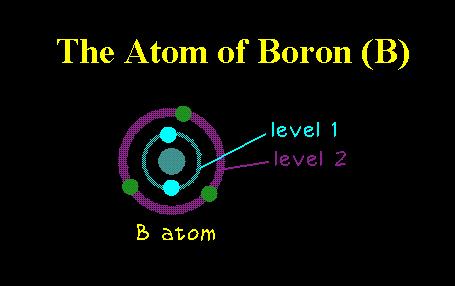
17 group (or family) 4 valence-band Electrons All elements in group have 4 valence-band electrons
18 Serves as an acceptor of electrons Acts as a p-type impurity when used as a silicon dopant All elements in group have 3 valence-band electrons Only 3 alenceband Electrons
19

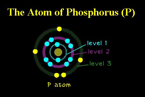
20 Serves as an donor of electrons Acts as an n-type impurity when used as a silicon dopant All elements in group have 5 valence-band electrons Five alenceband Electrons
21
22
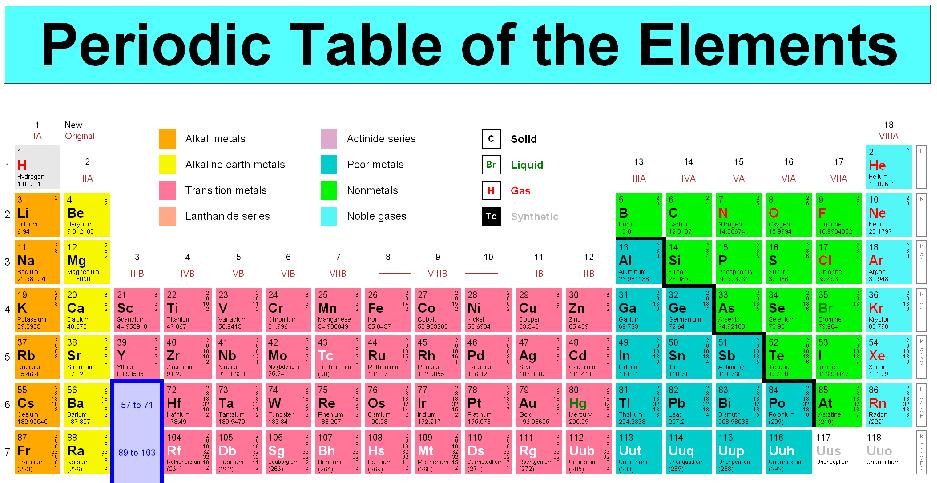
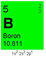
23 Silicon opants in Semiconductor Processes B (Boron) widely used a dopant for creating p-type regions P (Phosphorus) widely used a dopant for creating n-type regions (bulk doping, diffuses fast) As (Arsenic) widely used a dopant for creating n-type regions (Active region doping, diffuses slower)
24 iodes (pn junctions) epletion region created that is ionized but void of carriers
25 pn Junctions Physical Boundary Separating n-type and p-type regions f doping levels identical, depletion region extends equally into n-type and p-type regions
26 pn Junctions Physical Boundary Separating n-type and p-type regions Extends farther into p-type region if p-doping lower than n-doping
27 pn Junctions Physical Boundary Separating n-type and p-type regions Extends farther into n-type region if n-doping lower than p-doping
28 pn Junctions Positive voltages across the p to n junction are referred to forward bias Negative voltages across the p to n junction are referred to reverse bias As forward bias increases, depletion region thins and current starts to flow Current grows very rapidly as forward bias increases Current is very small under revere bias
29 pn Junctions Anode Anode Cathode Cathode Circuit Symbol
30 pn Junctions As forward bias increases, depletion region thins and current starts to flow Current grows very rapidly as forward bias increases Anode Cathode Simple iode Model: =0 >0 =0 <0 Simple model often referred to as the deal diode model
31 pn Junctions Simple iode Model: pn junction serves as a rectifier passing current in one direction and blocking it n the other direction
32 Rectifier Application: 1 OUT Simple iode Model: N 1K N = M sinωt M N t OUT M t
33 - characteristics of pn junction mproved iode Model: (signal or rectifier diode) d S in the 10fA to 100fA range d kt = t q iode Equation d t e 1 S What is t at room temp? t is about 26m at room temp k= (24) JK -1 q = (40) C k/q= K -1 iode equation due to William Schockley, inventor of BJT n 1919, William Henry Eccles coined the term diode n 1940, Russell Ohl stumbled upon the p-n junction diode
34 - characteristics of pn junction mproved iode Model: (signal or rectifier diode) iode Characteristics 0.01 d d d (amps) d (volts) iode Equation Under reverse bias ( d <0), Under forward bias ( d >0), d t e 1 S Simplification of iode Equation: S Se d t S in the 10fA to 100fA range kt = t q k= (24) JK -1 q = (40) C k/q= K -1 t is about 26m at room temp Simplification essentially identical model except for d very close to 0 iode Equation or forward bias simplification is unwieldy to work with analytically
35 - characteristics of pn junction mproved iode Model: iode Equation Simplification of iode Equation: Under reverse bias, Under forward bias, (signal or rectifier diode) d t e 1 S S S e d t S often in the 10fA to 100fA range S proportional to junction area t is about 26m at room temp How much error is introduced using the simplification for d > 0.5? d t S e 1 Se d t e 1 S d t e How much error is introduced using the simplification for d < - 0.5? e Simplification almost never introduces any significant error 9 9

36 Will you impress your colleagues or your boss if you use the more exact diode equation when d < -0.5 or d > +0.5? Will your colleagues or your boss be unimpressed if you use the more exact diode equation when d < -0.5 or d > +0.5?
37 pn Junctions Anode Cathode iode Equation: (good enough for most applications) JSAe 0 n T 0 0 Note: S =J s A J S = Sat Current ensity (in the 1aA/u 2 to 1fA/u 2 range) A= Junction Cross Section Area T =kt/q (k/q=1.381x10-23 C/ K/1.6x10-19 C=8.62x10⁻⁵ / K) n is approximately 1
38 pn Junctions iode Equation: J 0 S Ae n T 0 0 Anode J S is strongly temperature dependent With n=1, for >0, Cathode - G0 (T) J T m e Ae t t SX Typical values for key parameters: J SX =0.5A/μ 2, G0 =1.17, m=2.3
39 Example: pn Junctions - G0 (T) J m t T e Ae SX t What percent change in S will occur for a 1 C change in temperature at room temperature? - -G G0 G0 G0 G0 (T ) t T1 (T ) (T ) m m m m t T1 t 2 t t 2 t 2 J T e Ae - J T e Ae T e - T e SX T SX T T S S -G0 - - G0 G0 m t T1 (T ) m t T1 t 2 J T e Ae T e SX T T x x x10 S % 21% S
40 pn Junctions Anode Cathode iode Equation: (good enough for most applications) JSAe 0 n T 0 0 S =J s A Simple iode Model: Often termed the conducting or ON state Often termed the nonconducting or OFF state
41 Consider again the basic rectifier circuit OUT N R Previously considered sinusoidal excitation Previously gave qualitative analysis Rigorous analysis method is essential? O U T
42 Analysis of Nonlinear Circuits (Circuits with one or more nonlinear devices) What analysis tools or methods can be used? KCL? KL? Superposition? Nodal Analysis Mesh Analysis Two-Port Subcircuits oltage ivider? Current ivider? Thevenin and Norton Equivalent Circuits?
43 Consider again the basic rectifier circuit OUT N R N OUT R R d t e 1 S OUT S R e N t O U T 1 Even the simplest diode circuit does not have a closed-form solution when diode equation is used to model the diode!! ue to the nonlinear nature of the diode equation Simplifications are essential if analytical results are to be obtained
44 Lets study the diode equation a little further d t d S e 1 iode Characteristics d (amps) Linear-Linear Axis d (volts) Power issipation Becomes estructive if d > 0.85 (actually less)
45 Lets study the diode equation a little further d t e 1 d S iode Characteristics d (amps) E-06 1E-08 1E-10 1E-12 Linear-Log Axis d (volts) For two decades of current change, d is close to 0.6 This is the most useful current range for many applications
46 Lets study the diode equation a little further d t e 1 d S iode Characteristics 0.01 d (amps) d (volts) For two decades of current change, d is close to 0.6 This is the most useful current range when conducting for many applications
47 Lets study the diode equation a little further d d t e 1 S iode Characteristics d 0 d 0.6 d d d (amps) d (volts) Widely Used Piecewise Linear Model
48 Lets study the diode equation a little further d d t e 1 S iode Characteristics d (amps) d (volts) Better model in ON state though often not needed ncludes iode ON resistance
49 Lets study the diode equation a little further d t e 1 d S Piecewise Linear Model with iode Resistance d d 0 if 0.6 d R d d (R is rather small: often in the 20Ώ to 100Ώ range): if Equivalent Circuit A d C A C Off State d d A C d 0.6 R On State
50 The deal iode 0 if 0 0 if 0
51 The deal iode 0 if 0 0 if 0 OFF ON ON OFF alid for >0 0
52 iode Models d (amps) iode Characteristics d (volts) d (amps) iode Characteristics d (volts) iode Characteristics d (amps) d (volts) Which model should be used? The simplest model that will give acceptable results in the analysis of a circuit
53 iode Models iode Characteristics iode Equation d t e 1 S d (amps) d (volts) iode Characteristics d 0 d 0.6 if d if d d (amps) d (volts) iode Characteristics Piecewise Linear Models d d d R d if if d d d (amps) d (volts) 0 if 0 0 if 0
54 End of Lecture 12
EE 330 Lecture 13. Devices in Semiconductor Processes. Diodes
 EE 330 Lecture 13 evices in Semiconductor Processes iodes Exam 1 Friday Sept 22 Students may bring 1 page of notes Next weeks HW assignment due on Wed Sept 20 at beginning of class No 5:00 p.m extension
EE 330 Lecture 12. Devices in Semiconductor Processes. Diodes
 EE 330 Lecture 12 evices in Semiconuctor Processes ioes Review from Last Lecture http://www.ayah.com/perioic/mages/perioic%20table.png Review from Last Lecture Review from Last Lecture Silicon opants in
EE 330 Lecture 13. Devices in Semiconductor Processes. Diodes Capacitors Transistors
 EE 330 Lecture 13 evices in Semiconuctor Processes ioes Capacitors Transistors Review from Last Lecture pn Junctions Physical Bounary Separating n-type an p-type regions Extens farther into n-type region
EE 434 Lecture 13. Basic Semiconductor Processes Devices in Semiconductor Processes
 EE 434 Lecture 3 Basic Semiconductor Processes Devices in Semiconductor Processes Quiz 9 The top view of a device fabricated in a bulk CMOS process is shown in the figure below a) Identify the device b)
EE 434 Lecture 12. Process Flow (wrap up) Device Modeling in Semiconductor Processes
 Device Modeling in Semiconductor Processes") EE 434 Lecture 12 Process Flow (wrap up) Device Modeling in Semiconductor Processes Quiz 6 How have process engineers configured a process to assure that the thickness of the gate oxide for the p-channel
EE 434 Lecture 12 Process Flow (wrap up) Device Modeling in Semiconductor Processes Quiz 6 How have process engineers configured a process to assure that the thickness of the gate oxide for the p-channel
Semiconductor Physics fall 2012 problems
 Semiconductor Physics fall 2012 problems 1. An n-type sample of silicon has a uniform density N D = 10 16 atoms cm -3 of arsenic, and a p-type silicon sample has N A = 10 15 atoms cm -3 of boron. For each
EE 330 Lecture 14. Devices in Semiconductor Processes. Diodes Capacitors MOSFETs
 EE 330 Lecture 14 Devices in Semiconuctor Processes Dioes Capacitors MOSFETs Reminer: Exam 1 Friay Feb 16 Stuents may bring one page of notes (front an back) but no electronic ata storage or remote access
ECE321 Electronics I
 ECE321 Electronics I Lecture 4: Physics of Semiconductor iodes Payman Zarkesh-Ha Office: ECE Bldg. 230B Office hours: Tuesday 2:00-3:00PM or by appointment E-mail: pzarkesh.unm.edu Slide: 1 Review of Last
UNIVERSITY OF CALIFORNIA, BERKELEY College of Engineering Department of Electrical Engineering and Computer Sciences
 UNIVERSITY OF CALIFORNIA, BERKELEY College of Engineering Department of Electrical Engineering and Computer Sciences EECS 40 Spring 2000 Introduction to Microelectronic Devices Prof. King MIDTERM EXAMINATION
Lecture (02) PN Junctions and Diodes
 PN Junctions and Diodes") Lecture (02) PN Junctions and Diodes By: Dr. Ahmed ElShafee ١ I Agenda N type, P type semiconductors N Type Semiconductor P Type Semiconductor PN junction Energy Diagrams of the PN Junction and Depletion
Lecture (02) PN Junctions and Diodes By: Dr. Ahmed ElShafee ١ I Agenda N type, P type semiconductors N Type Semiconductor P Type Semiconductor PN junction Energy Diagrams of the PN Junction and Depletion
Lecture 0. EE206 Electronics I
 Lecture 0 Course Overview EE206 Electronics I Course description: Theory, characteristics and operation of diodes, bipolar junction transistors and MOSFET transistors. When: Tue Thu 10:30-12:20 (Lectures)
EE 330 Lecture 15. Devices in Semiconductor Processes. Diodes Capacitors MOSFETs
 EE 330 Lecture 15 evices in Semiconuctor Processes ioes Capacitors MOSFETs Review from Last Lecture Basic evices an evice Moels Resistor ioe Capacitor MOSFET BJT Review from Last Lecture Review from Last
ECE PN Junctions and Diodes
 ECE 342 2. PN Junctions and iodes Jose E. Schutt-Aine Electrical & Computer Engineering University of Illinois jschutt@emlab.uiuc.edu ECE 342 Jose Schutt Aine 1 B: material dependent parameter = 5.4 10
LECTURE 23. MOS transistor. 1 We need a smart switch, i.e., an electronically controlled switch. Lecture Digital Circuits, Logic
 LECTURE 23 Lecture 16-20 Digital Circuits, Logic 1 We need a smart switch, i.e., an electronically controlled switch 2 We need a gain element for example, to make comparators. The device of our dreams
UNIVERSITY OF CALIFORNIA, BERKELEY College of Engineering Department of Electrical Engineering and Computer Sciences
 UNIVERSITY OF CALIFORNIA, BERKELEY College of Engineering Department of Electrical Engineering and Computer Sciences EE 105: Microelectronic Devices and Circuits Spring 2008 MIDTERM EXAMINATION #1 Time
Junction Diodes. Tim Sumner, Imperial College, Rm: 1009, x /18/2006
 Junction Diodes Most elementary solid state junction electronic devices. They conduct in one direction (almost correct). Useful when one converts from AC to DC (rectifier). But today diodes have a wide
4. I-V characteristics of electric
 KL 4. - characteristics of electric conductors 4.1 ntroduction f an electric conductor is connected to a voltage source with voltage a current is produced. We define resistance being the ratio of the voltage
ITT Technical Institute ET215 Devices I Unit 1
 ITT Technical Institute ET215 Devices I Unit 1 Chapter 1 Chapter 2, Sections 2.1-2.4 Chapter 1 Basic Concepts of Analog Circuits Recall ET115 & ET145 Ohms Law I = V/R If voltage across a resistor increases
Electronics EC /2/2012. * In-class exams: 40% 7 th week exam 25% 12 th week exam 15%
 Arab Academy for Science, Technology and Maritime Transport Electronics EC 331 Dr. Mohamed Hassan Course Assessment * In-class exams: 40% 7 th week exam 25% 12 th week exam 15% *Tutorial exams and activities:
Semiconductor Devices and Circuits Fall Midterm Exam. Instructor: Dr. Dietmar Knipp, Professor of Electrical Engineering. Name: Mat. -Nr.
 Semiconductor Devices and Circuits Fall 2003 Midterm Exam Instructor: Dr. Dietmar Knipp, Professor of Electrical Engineering Name: Mat. -Nr.: Guidelines: Duration of the Midterm: 1 hour The exam is a closed
ESE 570: Digital Integrated Circuits and VLSI Fundamentals
 ESE 570: Digital Integrated Circuits and VLSI Fundamentals Lec 4: January 29, 2019 MOS Transistor Theory, MOS Model Penn ESE 570 Spring 2019 Khanna Lecture Outline! CMOS Process Enhancements! Semiconductor
EECS130 Integrated Circuit Devices
 EECS130 Integrated Circuit Devices Professor Ali Javey 9/18/2007 P Junctions Lecture 1 Reading: Chapter 5 Announcements For THIS WEEK OLY, Prof. Javey's office hours will be held on Tuesday, Sept 18 3:30-4:30
ESE 570: Digital Integrated Circuits and VLSI Fundamentals
 ESE 570: Digital Integrated Circuits and VLSI Fundamentals Lec 4: January 23, 2018 MOS Transistor Theory, MOS Model Penn ESE 570 Spring 2018 Khanna Lecture Outline! CMOS Process Enhancements! Semiconductor
Introduction to Transistors. Semiconductors Diodes Transistors
 Introduction to Transistors Semiconductors Diodes Transistors 1 Semiconductors Typical semiconductors, like silicon and germanium, have four valence electrons which form atomic bonds with neighboring atoms
Lecture (02) Introduction to Electronics II, PN Junction and Diodes I
 Introduction to Electronics II, PN Junction and Diodes I") Lecture (02) Introduction to Electronics II, PN Junction and Diodes I By: Dr. Ahmed ElShafee ١ Agenda Current in semiconductors/conductors N type, P type semiconductors N Type Semiconductor P Type Semiconductor
Lecture (02) Introduction to Electronics II, PN Junction and Diodes I By: Dr. Ahmed ElShafee ١ Agenda Current in semiconductors/conductors N type, P type semiconductors N Type Semiconductor P Type Semiconductor
The Devices. Digital Integrated Circuits A Design Perspective. Jan M. Rabaey Anantha Chandrakasan Borivoje Nikolic. July 30, 2002
 igital Integrated Circuits A esign Perspective Jan M. Rabaey Anantha Chandrakasan Borivoje Nikolic The evices July 30, 2002 Goal of this chapter Present intuitive understanding of device operation Introduction
Lecture 1. OUTLINE Basic Semiconductor Physics. Reading: Chapter 2.1. Semiconductors Intrinsic (undoped) silicon Doping Carrier concentrations
 silicon Doping Carrier concentrations") Lecture 1 OUTLINE Basic Semiconductor Physics Semiconductors Intrinsic (undoped) silicon Doping Carrier concentrations Reading: Chapter 2.1 EE105 Fall 2007 Lecture 1, Slide 1 What is a Semiconductor? Low
Lecture 1 OUTLINE Basic Semiconductor Physics Semiconductors Intrinsic (undoped) silicon Doping Carrier concentrations Reading: Chapter 2.1 EE105 Fall 2007 Lecture 1, Slide 1 What is a Semiconductor? Low
EE301 Electronics I , Fall
 EE301 Electronics I 2018-2019, Fall 1. Introduction to Microelectronics (1 Week/3 Hrs.) Introduction, Historical Background, Basic Consepts 2. Rewiev of Semiconductors (1 Week/3 Hrs.) Semiconductor materials
Classification of Solids
 Classification of Solids Classification by conductivity, which is related to the band structure: (Filled bands are shown dark; D(E) = Density of states) Class Electron Density Density of States D(E) Examples
Lecture 04 Review of MOSFET
 ECE 541/ME 541 Microelectronic Fabrication Techniques Lecture 04 Review of MOSFET Zheng Yang (ERF 3017, email: yangzhen@uic.edu) What is a Transistor? A Switch! An MOS Transistor V GS V T V GS S Ron D
EE 330 Lecture 22. Small Signal Modelling Operating Points for Amplifier Applications Amplification with Transistor Circuits
 EE 330 Lecture 22 Small Signal Modelling Operating Points for Amplifier Applications Amplification with Transistor Circuits Exam 2 Friday March 9 Exam 3 Friday April 13 Review Session for Exam 2: 6:00
SEMICONDUCTORS. Conductivity lies between conductors and insulators. The flow of charge in a metal results from the
 SEMICONDUCTORS Conductivity lies between conductors and insulators The flow of charge in a metal results from the movement of electrons Electros are negatively charged particles (q=1.60x10⁻¹⁹ C ) The outermost
Diodes. anode. cathode. cut-off. Can be approximated by a piecewise-linear-like characteristic. Lecture 9-1
 Diodes mplest nonlinear circuit element Basic operation sets the foundation for Bipolar Junction Transistors (BJTs) Also present in Field Effect Transistors (FETs) Ideal diode characteristic anode cathode
2. (2pts) What is the major reason that contacts from metal to poly are not allowed on top of the gate of a transistor?
 What is the major reason that contacts from metal to poly are not allowed on top of the gate of a transistor?") EE 330 Exam 1 Spring 2018 Name Instructions: Students may bring 1 page of notes (front and back) to this exam and a calculator but the use of any device that has wireless communication capability is prohibited.
EE 330 Exam 1 Spring 2018 Name Instructions: Students may bring 1 page of notes (front and back) to this exam and a calculator but the use of any device that has wireless communication capability is prohibited.
Session 0: Review of Solid State Devices. From Atom to Transistor
 Session 0: Review of Solid State Devices From Atom to Transistor 1 Objective To Understand: how Diodes, and Transistors operate! p n p+ n p- n+ n+ p 2 21 Century Alchemy! Ohm s law resistivity Resistivity
Chap. 11 Semiconductor Diodes
 Chap. 11 Semiconductor Diodes Semiconductor diodes provide the best resolution for energy measurements, silicon based devices are generally used for charged-particles, germanium for photons. Scintillators
Quiz #1 Practice Problem Set
 Name: Student Number: ELEC 3908 Physical Electronics Quiz #1 Practice Problem Set? Minutes January 22, 2016 - No aids except a non-programmable calculator - All questions must be answered - All questions
! CMOS Process Enhancements. ! Semiconductor Physics. " Band gaps. " Field Effects. ! MOS Physics. " Cut-off. " Depletion.
 ESE 570: Digital Integrated Circuits and VLSI Fundamentals Lec 4: January 9, 019 MOS Transistor Theory, MOS Model Lecture Outline CMOS Process Enhancements Semiconductor Physics Band gaps Field Effects
n N D n p = n i p N A
 Summary of electron and hole concentration in semiconductors Intrinsic semiconductor: E G n kt i = pi = N e 2 0 Donor-doped semiconductor: n N D where N D is the concentration of donor impurity Acceptor-doped
ELECTRONIC DEVICES AND CIRCUITS SUMMARY
 ELECTRONIC DEVICES AND CIRCUITS SUMMARY Classification of Materials: Insulator: An insulator is a material that offers a very low level (or negligible) of conductivity when voltage is applied. Eg: Paper,
Section 12: Intro to Devices
 Section 12: Intro to Devices Extensive reading materials on reserve, including Robert F. Pierret, Semiconductor Device Fundamentals Bond Model of Electrons and Holes Si Si Si Si Si Si Si Si Si Silicon
Chemistry Instrumental Analysis Lecture 8. Chem 4631
 Chemistry 4631 Instrumental Analysis Lecture 8 UV to IR Components of Optical Basic components of spectroscopic instruments: stable source of radiant energy transparent container to hold sample device
EE 230 Lecture 20. Nonlinear Op Amp Applications. The Comparator Nonlinear Analysis Methods
 EE 230 Lecture 20 Nonlinear Op Amp Applications The Comparator Nonlinear Analysis Methods Quiz 14 What is the major purpose of compensation when designing an operatinal amplifier? And the number is? 1
Review Energy Bands Carrier Density & Mobility Carrier Transport Generation and Recombination
 Review Energy Bands Carrier Density & Mobility Carrier Transport Generation and Recombination The Metal-Semiconductor Junction: Review Energy band diagram of the metal and the semiconductor before (a)
EECS130 Integrated Circuit Devices
 EECS130 Integrated Circuit Devices Professor Ali Javey 10/02/2007 MS Junctions, Lecture 2 MOS Cap, Lecture 1 Reading: finish chapter14, start chapter16 Announcements Professor Javey will hold his OH at
Semiconductor Physics fall 2012 problems
 Semiconductor Physics fall 2012 problems 1. An n-type sample of silicon has a uniform density N D = 10 16 atoms cm -3 of arsenic, and a p-type silicon sample has N A = 10 15 atoms cm -3 of boron. For each
UNIVERSITY OF CALIFORNIA College of Engineering Department of Electrical Engineering and Computer Sciences. EECS 130 Professor Ali Javey Fall 2006
 UNIVERSITY OF CALIFORNIA College of Engineering Department of Electrical Engineering and Computer Sciences EECS 130 Professor Ali Javey Fall 2006 Midterm I Name: Closed book. One sheet of notes is allowed.
For the following statements, mark ( ) for true statement and (X) for wrong statement and correct it.
 for true statement and (X) for wrong statement and correct it.") Benha University Faculty of Engineering Shoubra Electrical Engineering Department First Year communications. Answer all the following questions Illustrate your answers with sketches when necessary. The
Benha University Faculty of Engineering Shoubra Electrical Engineering Department First Year communications. Answer all the following questions Illustrate your answers with sketches when necessary. The
ECE-342 Test 2 Solutions, Nov 4, :00-8:00pm, Closed Book (one page of notes allowed)
") ECE-342 Test 2 Solutions, Nov 4, 2008 6:00-8:00pm, Closed Book (one page of notes allowed) Please use the following physical constants in your calculations: Boltzmann s Constant: Electron Charge: Free
ECE-342 Test 2 Solutions, Nov 4, 2008 6:00-8:00pm, Closed Book (one page of notes allowed) Please use the following physical constants in your calculations: Boltzmann s Constant: Electron Charge: Free
Diodes. EE223 Digital & Analogue Electronics Derek Molloy 2012/2013.
 Diodes EE223 Digital & Analogue Electronics Derek Molloy 2012/2013 Derek.Molloy@dcu.ie Diodes: A Semiconductor? Conductors Such as copper, aluminium have a cloud of free electrons weak bound valence electrons
Electronic Circuits for Mechatronics ELCT 609 Lecture 2: PN Junctions (1)
") Electronic Circuits for Mechatronics ELCT 609 Lecture 2: PN Junctions (1) Assistant Professor Office: C3.315 E-mail: eman.azab@guc.edu.eg 1 Electronic (Semiconductor) Devices P-N Junctions (Diodes): Physical
Electronic Circuits for Mechatronics ELCT 609 Lecture 2: PN Junctions (1) Assistant Professor Office: C3.315 E-mail: eman.azab@guc.edu.eg 1 Electronic (Semiconductor) Devices P-N Junctions (Diodes): Physical
6.012 Electronic Devices and Circuits
 Page 1 of 12 YOUR NAME Department of Electrical Engineering and Computer Science Massachusetts Institute of Technology 6.012 Electronic Devices and Circuits FINAL EXAMINATION Open book. Notes: 1. Unless
Course Administration. CPE/EE 427, CPE 527 VLSI Design I L04: MOS Transistors. Review: CMOS Process at a Glance
 Course Administration CPE/EE 7, CPE 7 VLI esign I L: MO Transistors epartment of Electrical and Computer Engineering University of Alabama in Huntsville Aleksandar Milenkovic ( www.ece.uah.edu/~milenka
! CMOS Process Enhancements. ! Semiconductor Physics. " Band gaps. " Field Effects. ! MOS Physics. " Cut-off. " Depletion.
 ESE 570: Digital Integrated Circuits and VLSI Fundamentals Lec 4: January 3, 018 MOS Transistor Theory, MOS Model Lecture Outline! CMOS Process Enhancements! Semiconductor Physics " Band gaps " Field Effects!
1st Year-Computer Communication Engineering-RUC. 4- P-N Junction
 4- P-N Junction We begin our study of semiconductor devices with the junction for three reasons. (1) The device finds application in many electronic systems, e.g., in adapters that charge the batteries
Electrical Resistance
 Electrical Resistance I + V _ W Material with resistivity ρ t L Resistance R V I = L ρ Wt (Unit: ohms) where ρ is the electrical resistivity 1 Adding parts/billion to parts/thousand of dopants to pure
Semiconductors. Semiconductors also can collect and generate photons, so they are important in optoelectronic or photonic applications.
 Semiconductors Semiconducting materials have electrical properties that fall between true conductors, (like metals) which are always highly conducting and insulators (like glass or plastic or common ceramics)
CLASS 12th. Semiconductors
 CLASS 12th Semiconductors 01. Distinction Between Metals, Insulators and Semi-Conductors Metals are good conductors of electricity, insulators do not conduct electricity, while the semiconductors have
5. Semiconductors and P-N junction
 5. Semiconductors and P-N junction Thomas Zimmer, University of Bordeaux, France Summary Learning Outcomes... 2 Physical background of semiconductors... 2 The silicon crystal... 2 The energy bands... 3
VLSI Design I; A. Milenkovic 1
 Review: implified CMO Inverter Process CPE/EE 7, CPE 7 VLI esign I L: MO Transistor cut line epartment of Electrical and Computer Engineering University of Alabama in Huntsville Aleksandar Milenkovic (
Introduction to Semiconductor Physics. Prof.P. Ravindran, Department of Physics, Central University of Tamil Nadu, India
 Introduction to Semiconductor Physics 1 Prof.P. Ravindran, Department of Physics, Central University of Tamil Nadu, India http://folk.uio.no/ravi/cmp2013 Review of Semiconductor Physics Semiconductor fundamentals
Electronics The basics of semiconductor physics
 Electronics The basics of semiconductor physics Prof. Márta Rencz, Gergely Nagy BME DED September 16, 2013 The basic properties of semiconductors Semiconductors conductance is between that of conductors
Diodes for Power Electronic Applications
 Lecture Notes Diodes for Power Electronic Applications William P. Robbins Professor, Dept. of Electrical and Computer Engineering University of Minnesota OUTLINE PN junction power diode construction Breakdown
Solid State Electronics. Final Examination
 The University of Toledo EECS:4400/5400/7400 Solid State Electronic Section elssf08fs.fm - 1 Solid State Electronics Final Examination Problems Points 1. 1. 14 3. 14 Total 40 Was the exam fair? yes no
Tunnel Diodes (Esaki Diode)
") Tunnel Diodes (Esaki Diode) Tunnel diode is the p-n junction device that exhibits negative resistance. That means when the voltage is increased the current through it decreases. Esaki diodes was named
Tunnel Diodes (Esaki Diode) Tunnel diode is the p-n junction device that exhibits negative resistance. That means when the voltage is increased the current through it decreases. Esaki diodes was named
ISSUES TO ADDRESS...
 Chapter 12: Electrical Properties School of Mechanical Engineering Choi, Hae-Jin Materials Science - Prof. Choi, Hae-Jin Chapter 12-1 ISSUES TO ADDRESS... How are electrical conductance and resistance
Chapter 2 The Well 9/5/2017. E E 480 Introduction to Analog and Digital VLSI Paul M. Furth New Mexico State University
 hapter 2 The Well E E 480 Introduction to Analog and Digital VLSI Paul M. Furth New Mexico State University p+ sub ~ 150 m thick, p-epi ~ 30 m thick All transistors go in p- epi layer Typical p- doping
The Intrinsic Silicon
 The Intrinsic ilicon Thermally generated electrons and holes Carrier concentration p i =n i ni=1.45x10 10 cm-3 @ room temp Generally: n i = 3.1X10 16 T 3/2 e -1.21/2KT cm -3 T= temperature in K o (egrees
Nature of Lesson (Lecture/Tutorial) H3 WK No. Day/ Date. Remarks. Duration. 4.00pm 6.30pm ALL. 2.5 hours. Introduction to Semiconductors Lecture 01
 H3 WK No. Day/ Date. Remarks. Duration. 4.00pm 6.30pm ALL. 2.5 hours. Introduction to Semiconductors Lecture 01") JANUARY 2018 INTAKE Subject : Semiconductor Physics & Devices Venue : HCI Schedule : Mondays for Tutorial (3pm 5pm / 5pm 7pm) or Tuesdays for Tutorial (3pm 5pm / 5pm 7pm) and Thursdays for Lecture (4pm-6.30
JANUARY 2018 INTAKE Subject : Semiconductor Physics & Devices Venue : HCI Schedule : Mondays for Tutorial (3pm 5pm / 5pm 7pm) or Tuesdays for Tutorial (3pm 5pm / 5pm 7pm) and Thursdays for Lecture (4pm-6.30
Semiconductor Physics Problems 2015
 Semiconductor Physics Problems 2015 Page and figure numbers refer to Semiconductor Devices Physics and Technology, 3rd edition, by SM Sze and M-K Lee 1. The purest semiconductor crystals it is possible
PN Junction
 P Junction 2017-05-04 Definition Power Electronics = semiconductor switches are used Analogue amplifier = high power loss 250 200 u x 150 100 u Udc i 50 0 0 50 100 150 200 250 300 350 400 i,u dc i,u u
Semiconductor Detectors
 Semiconductor Detectors Summary of Last Lecture Band structure in Solids: Conduction band Conduction band thermal conductivity: E g > 5 ev Valence band Insulator Charge carrier in conductor: e - Charge
Section 12: Intro to Devices
 Section 12: Intro to Devices Extensive reading materials on reserve, including Robert F. Pierret, Semiconductor Device Fundamentals EE143 Ali Javey Bond Model of Electrons and Holes Si Si Si Si Si Si Si
Digital Electronics Part II - Circuits
 Digital Electronics Part - Circuits Dr.. J. Wassell Gates from Transistors ntroduction Logic circuits are non-linear, consequently we will introduce a graphical technique for analysing such circuits The
Introduction to Semiconductor Devices
 Physics 233 Experiment 48 Introduction to Semiconductor Devices References 1. G.W. Neudeck, The PN Junction Diode, Addison-Wesley MA 1989 2. Background notes (Appendix A) 3. Specification sheet for Diode
2. (2pts) What is the major difference between an epitaxial layer and a polysilicon layer?
 What is the major difference between an epitaxial layer and a polysilicon layer?") EE 330 Exam 1 Spring 2017 Name Instructions: Students may bring 1 page of notes (front and back) to this exam and a calculator but the use of any device that has wireless communication capability is prohibited.
EE 330 Exam 1 Spring 2017 Name Instructions: Students may bring 1 page of notes (front and back) to this exam and a calculator but the use of any device that has wireless communication capability is prohibited.
Introduction to Semiconductor Devices
 Physics 233 Experiment 48 Introduction to Semiconductor Devices References 1. G.W. Neudeck, The PN Junction Diode, Addison-Wesley MA 1989 2. Background notes (Appendix A) 3. Specification sheet for Diode
Lecture 2. Semiconductor Physics. Sunday 4/10/2015 Semiconductor Physics 1-1
 Lecture 2 Semiconductor Physics Sunday 4/10/2015 Semiconductor Physics 1-1 Outline Intrinsic bond model: electrons and holes Charge carrier generation and recombination Intrinsic semiconductor Doping:
L03: pn Junctions, Diodes
 8/30/2012 Page 1 of 5 Reference:C:\Users\Bernhard Boser\Documents\Files\Lib\MathCAD\Default\defaults.mcd L03: pn Junctions, Diodes Intrinsic Si Q: What are n, p? Q: Is the Si charged? Q: How could we make
Extensive reading materials on reserve, including
 Section 12: Intro to Devices Extensive reading materials on reserve, including Robert F. Pierret, Semiconductor Device Fundamentals EE143 Ali Javey Bond Model of Electrons and Holes Si Si Si Si Si Si Si
Lecture 15 OUTLINE. MOSFET structure & operation (qualitative) Review of electrostatics The (N)MOS capacitor
 Review of electrostatics The (N)MOS capacitor") Lecture 15 OUTLINE MOSFET structure & operation (qualitative) Review of electrostatics The (N)MOS capacitor Electrostatics t ti Charge vs. voltage characteristic Reading: Chapter 6.1 6.2.1 EE105 Fall 2007
Lecture 15 OUTLINE MOSFET structure & operation (qualitative) Review of electrostatics The (N)MOS capacitor Electrostatics t ti Charge vs. voltage characteristic Reading: Chapter 6.1 6.2.1 EE105 Fall 2007
EE105 Fall 2015 Microelectronic Devices and Circuits: Semiconductor Fabrication and PN Junctions
 EE105 Fall 2015 Microelectronic Devices and Circuits: Semiconductor Fabrication and PN Junctions Prof. Ming C. Wu wu@eecs.berkeley.edu 511 Sutardja Dai Hall (SDH) 1 pn Junction p-type semiconductor in
electronics fundamentals
 electronics fundamentals circuits, devices, and applications THOMAS L. FLOYD DAVID M. BUCHLA Lesson 1: Diodes and Applications Semiconductors Figure 1-1 The Bohr model of an atom showing electrons in orbits
4/27 Friday. I have all the old homework if you need to collect them.
 4/27 Friday Last HW: do not need to turn it. Solution will be posted on the web. I have all the old homework if you need to collect them. Final exam: 7-9pm, Monday, 4/30 at Lambert Fieldhouse F101 Calculator
ECE 340 Lecture 27 : Junction Capacitance Class Outline:
 ECE 340 Lecture 27 : Junction Capacitance Class Outline: Breakdown Review Junction Capacitance Things you should know when you leave M.J. Gilbert ECE 340 Lecture 27 10/24/11 Key Questions What types of
Electro - Principles I
 Electro - Principles I Page 10-1 Atomic Theory It is necessary to know what goes on at the atomic level of a semiconductor so the characteristics of the semiconductor can be understood. In many cases a
UC DAVIS. Circuits I Course Outline
 UC DAVIS Circuits I Course Outline ENG 17 Professor Spencer Fall 2010 2041 Kemper Hall Lecture: MWF 4:10-5:00, 1003 Giedt Hall 752-6885 Discussion Section 1: W 1:10-2:00, 55 Roessler CRN: 61417 Discussion
U1 is zero based because its noninverting terminal is connected to circuit common. Therefore, the circuit reference voltage is 0 V.
 When you have completed this exercise, you will be able to operate a zener-clamped op amp comparator circuit using dc and ac voltages. You will verify your results with an oscilloscope. U1 is zero based
Department of Electrical and Computer Engineering, Cornell University. ECE 3150: Microelectronics. Spring Due on March 01, 2018 at 7:00 PM
 Department of Electrical and Computer Engineering, Cornell University ECE 3150: Microelectronics Spring 2018 Homework 4 Due on March 01, 2018 at 7:00 PM Suggested Readings: a) Lecture notes Important Note:
Basic Physics of Semiconductors
 Basic Physics of Semiconductors Semiconductor materials and their properties PN-junction diodes Reverse Breakdown EEM 205 Electronics I Dicle University, EEE Dr. Mehmet Siraç ÖZERDEM Semiconductor Physics
B. Both A and R are correct but R is not correct explanation of A. C. A is true, R is false. D. A is false, R is true
 1. Assertion (A): A demultiplexer can be used as a decode r. Reason (R): A demultiplexer can be built by using AND gates only. A. Both A and R are correct and R is correct explanation of A B. Both A and
Lecture 15 OUTLINE. MOSFET structure & operation (qualitative) Review of electrostatics The (N)MOS capacitor
 Review of electrostatics The (N)MOS capacitor") Lecture 15 OUTLINE MOSFET structure & operation (qualitative) Review of electrostatics The (N)MOS capacitor Electrostatics Charge vs. voltage characteristic Reading: Chapter 6.1 6.2.1 EE15 Spring 28 Lecture
Lecture 15 OUTLINE MOSFET structure & operation (qualitative) Review of electrostatics The (N)MOS capacitor Electrostatics Charge vs. voltage characteristic Reading: Chapter 6.1 6.2.1 EE15 Spring 28 Lecture
Lecture 6 PN Junction and MOS Electrostatics(III) Metal-Oxide-Semiconductor Structure
 Metal-Oxide-Semiconductor Structure") Lecture 6 PN Junction and MOS Electrostatics(III) Metal-Oxide-Semiconductor Structure Outline 1. Introduction to MOS structure 2. Electrostatics of MOS in thermal equilibrium 3. Electrostatics of MOS with
Lecture 6 PN Junction and MOS Electrostatics(III) Metal-Oxide-Semiconductor Structure Outline 1. Introduction to MOS structure 2. Electrostatics of MOS in thermal equilibrium 3. Electrostatics of MOS with
Unit IV Semiconductors Engineering Physics
 Introduction A semiconductor is a material that has a resistivity lies between that of a conductor and an insulator. The conductivity of a semiconductor material can be varied under an external electrical
B.Supmonchai June 26, q Introduction of device basic equations. q Introduction of models for manual analysis.
 June 26, 2004 oal of this chapter Chapter 2 MO Transistor Theory oonchuay upmonchai Integrated esign Application Research (IAR) Laboratory June 16th, 2004; Revised June 16th, 2005 q Present intuitive understanding
Homework 3 Solution. Due Friday (5pm), Feb. 14, 2013
, Feb. 14, 2013") University of California, Berkeley Spring 2013 EE 42/100 Prof. K. Pister Homework 3 Solution Due Friday (5pm), Feb. 14, 2013 Please turn the homework in to the drop box located next to 125 Cory Hall (labeled
University of California, Berkeley Spring 2013 EE 42/100 Prof. K. Pister Homework 3 Solution Due Friday (5pm), Feb. 14, 2013 Please turn the homework in to the drop box located next to 125 Cory Hall (labeled
Chapter 1 INTRODUCTION SEMICONDUCTORS MATERIAL
 Chapter 1 INTRODUCTION TO SEMICONDUCTORS MATERIAL Objectives Discuss basic structures of atoms Discuss properties of insulators, conductors, and semiconductors Discuss covalent bonding Describe the conductions
Electrical Characteristics of MOS Devices
 Electrical Characteristics of MOS Devices The MOS Capacitor Voltage components Accumulation, Depletion, Inversion Modes Effect of channel bias and substrate bias Effect of gate oide charges Threshold-voltage
12/10/09. Chapter 18: Electrical Properties. View of an Integrated Circuit. Electrical Conduction ISSUES TO ADDRESS...
 Chapter 18: Electrical Properties ISSUES TO ADDRESS... How are electrical conductance and resistance characterized? What are the physical phenomena that distinguish? For metals, how is affected by and
E2.2 Analogue Electronics
 E2.2 Analogue Electronics Instructor : Christos Papavassiliou Office, email : EE 915, c.papavas@imperial.ac.uk Lectures : Monday 2pm, room 408 (weeks 2-11) Thursday 3pm, room 509 (weeks 4-11) Problem,