EE 505 Lecture 7. Spectral Performance of Data Converters - Time Quantization - Amplitude Quantization Clock Jitter Statistical Circuit Modeling
|
|
|
- Jonas Stafford
- 5 years ago
- Views:
Transcription
1 EE 505 Lecture 7 Spectral Performance of Data Converters - Time Quantization - Amplitude Quantization Clock Jitter Statistical Circuit Modeling

2 . Review from last lecture. MatLab comparison: 512 Samples with Standard Sweep Spectre Results MatLab Results
3 . Review from last lecture. MatLab comparison: 512 Samples with Strobe Period Sweep Spectre Results MatLab Results
4 . Review from last lecture. Comparison of 4 windows

5 . Review from last lecture. Comparison of 4 windows
6 . Review from last lecture. Preliminary Observations about Windows Provide separation of spectral components Energy can be accumulated around spectral components Simple to apply Some windows work much better than others But windows do not provide dramatic improvement and can significantly degrade performance if sampling hypothesis are met
7 . Review from last lecture. Post-processing Method of circumventing the coherent sampling problem Can also be used for addressing spectral purity problem for test signal generation x kt S N 1 k 0 Post-Processor Χ k N 1 k 0 Non-coherent Easily implemented in MATLAB Will be considered in the laboratory Removes fundamental from samples and replaces with coherent fundamental before taking DFT
8 Spectral Characterization of Data Converters Distortion Analysis Time Quantization Effects of DACs of ADCs Amplitude Quantization Effects of DACs of ADCs Clock Jitter
9 Quantization Effects (time and amplitude depicted) 16,384 pts res = 4bits N P =25 20 msec
 16,384 pts res = 4bits N P =25 20")
10 Quantization Effects (time and amplitude depicted) 16,384 pts res = 4bits N P =25 20 msec
11 Quantization Effects (time and amplitude depicted) 16,384 pts res = 4bits
12 Quantization Effects (time and amplitude depicted) Simulation environment: N P =23 f SIG =50Hz V REF : -1V, 1V Res: will be varied N=2 n will be varied
13 Spectral Characterization of Data Converters Distortion Analysis Time Quantization Effects of DACs of ADCs Amplitude Quantization Effects of DACs of ADCs Clock Jitter

14 Quantization Effects Res = 4 bits
15 Quantization Effects Res = 4 bits Axis of Symmetry
16 Quantization Effects Res = 4 bits
17 Quantization Effects Res = 4 bits
18 Quantization Effects Res = 4 bits
19 Quantization Effects Res = 4 bits Expect quantization noise effects to be uniformly distributed!!
20 Quantization Effects Res = 4 bits Expect quantization noise effects to be uniformly distributed!!
21 Quantization Effects Res = 4 bits Expect quantization noise effects to be uniformly distributed!!
22 Quantization Effects Res = 4 bits Note presence of odd-ordered harmonic terms!!
23 Res = 4 bits Why are there spectral components present in the quantization noise? Recall the uncorrelated assumption was good only for about 4 bits or more!
24 Quantization Effects Res = 10 bits Quantization noise is much more uniform
25 Quantization Effects Res = 10 bits
26 Quantization Effects Res = 10 bits Harmonic Components not Visible
27 . Review from last lecture. Quantization Effects Res = 10 bits Compared to the previous slide, it appears that the quantization noise has gone down why does this occur?
28 Quantization Effects Res = 10 bits Compared to the previous slide, it appears that the quantization noise has gone down even more why does this occur?
29 Quantization Effects Res = 10 bits Compared to the previous slides, it appears that the quantization noise has gone down even more why does this occur?
30 Quantization Effects Res = 10 bits
31 Quantization Effects Res = 10 bits Very small third harmonic component but does not extend above other noise terms
32 . Review from last lecture. Spectral Characterization Amplitude Quantization Does not introduce spectral components for n large Nearly uniformly distributed Decreases with increasing N
33 Spectral Characterization of Data Converters Distortion Analysis Time Quantization Effects of DACs of ADCs Amplitude Quantization Effects of DACs of ADCs Clock Jitter
34 Spectral Characteristics of DACs and ADCs
35 Spectral Characteristics of DAC t Periodic Input Signal Sampling Clock T SIG t Sampled Input Signal (showing time points where samples taken)
36 Spectral Characteristics of DAC T SIG Quantization Levels T PERIOD Quantized Sampled Input Signal (with zero-order sample and hold)
37 Spectral Characteristics of DAC T DFT WINDOW T PERIOD T SIG T CLOCK Sampling Clock T DFT CLOCK DFT Clock
38 Spectral Characteristics of DAC T DFT WINDOW T PERIOD T SIG T CLOCK Sampling Clock T DFT CLOCK DFT Clock
39 Spectral Characteristics of DAC Sampling Clock DFT Clock
40 Spectral Characteristics of DAC Sampled Quantized Signal (zoomed) DFT Clock Sampling Clock
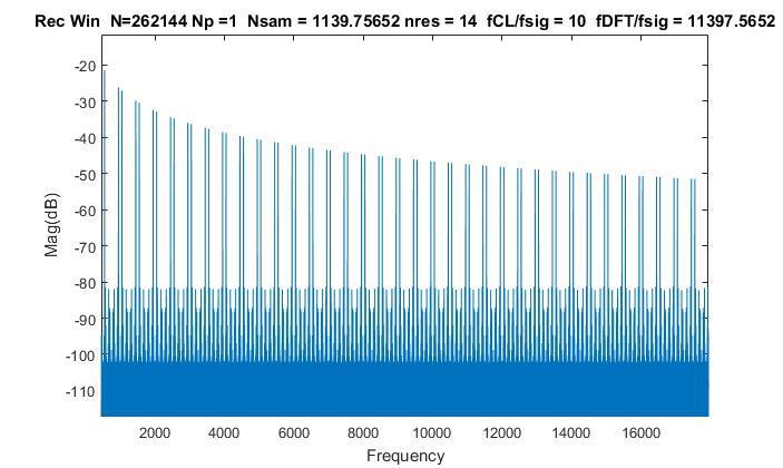
41 Spectral Characteristics of DAC Consider the following example f SIG =50 Hz f CL =500 Hz (DAC clock) f DFTCL =71.24K Hz n DFT =15 (coherent sampling) N P1 =23 (number of signal periods in DFT window) N P =1 n res =8 bits Xin(t) =.95sin(2πf SIG t) (-.4455dB) Matlab File: afft_quantization_dac_jan2017.m
42 DFT Simulation from Matlab n sam =
43 DFT Simulation from Matlab Expanded View n sam = Width of this region is f CL Analogous to the overall DFT window when directly sampled but modestly asymmetric

44 DFT Simulation from Matlab Expanded View n sam =
45 DFT Simulation from Matlab Expanded View n sam =
46 DAC Comparisons with Quantization Fundamental, second harmonic, and third harmonic N θ Nsam n A 1 A 2 A 3 32K K
47 Spectral Characteristics of DAC Consider the following example f SIG =50 Hz f CL =500 Hz (DAC clock) f DFTCL =71.24K Hz n DFT =18 (coherent sampling) N P1 =23 (number of signal periods in DFT window) N P =1 n res =8 bits Xin(t) =.95sin(2πf SIG t) (-.4455dB) Matlab File: afft_quantization_dac.m
48 DFT Simulation from Matlab n sam =
49 DFT Simulation from Matlab Expanded View n sam =
50 DFT Simulation from Matlab Expanded View n sam =
51 DFT Simulation from Matlab Expanded View n sam =
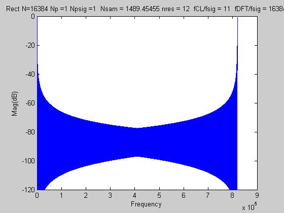
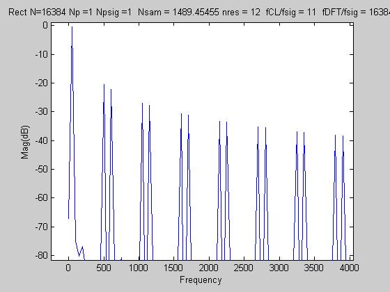
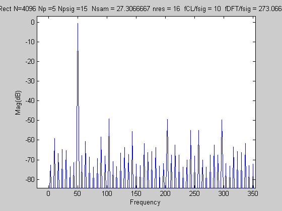
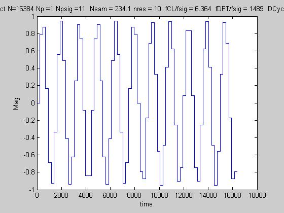
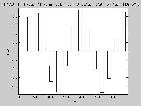
52 Spectral Characteristics of DAC Consider the following example f SIG =50 Hz f CL =500 Hz (DAC clock) f DFTCL =71.24K Hz n DFT =18 (coherent sampling) N P1 =23 (number of signal periods in DFT window) N P =1 n res =14bits Xin(t) =.95sin(2πf SIG t) (-.4455dB) Matlab File: afft_quantization_dac.m
53
54
55
56 Spectral Characteristics of DAC Consider the following example f SIG =50 Hz f CL =500 Hz (DAC clock) f DFTCL =71.24K Hz n DFT =18 (coherent sampling) N P1 =23 (number of signal periods in DFT window) N P =1 n res =16bits Xin(t) =.95sin(2πf SIG t) (-.4455dB) Matlab File: afft_quantization_dac.m
57
58
59
60 Spectral Characteristics of DAC Consider the following example f SIG =50 Hz f CL =497.8 Hz (DAC clock) f DFTCL = K Hz n DFT =16 (not coherent sampling) N P1 =23 (number of signal periods in DFT window) N P =1 n res =16bits Xin(t) =.95sin(2πf SIG t) (-.4455dB) Matlab File: afft_quantization_dac.m

61 DFT Simulation from Matlab

62 DFT Simulation from Matlab
63 DFT Simulation from Matlab
64 Skip to Next Separator
65 The spectral characteristics of DACs as affected by DAC clock rate, by DAC resolution, and by the length of the DFT window will be considered
66 Notation: T CL : Clock Period (=1/f CL ) T SIG : Signal Period (=1/f SIG ) T DFT : DFT period (=1/f DFT ) N SIG1 : Number of Signal Periods to establish periodicity with sampling clock N CL1 : Number of Clock Periods to establish periodicity with sampling clock N SIG : Number of Signal Periods in DFT window N CL : Number of Clock Periods in DFT window N P : Number of Periods in DFT window N SAM : Number of DFT samples in each clock period n: Length of DFT window in binary bits N: Length of DFT window n Q Number of binary bits of quantization
67 Graphical Interpretation of Signals for DAC Spectral Characterization T PERIOD T DFT Window T SIG T CLK T DFT Signal Clock Time Quantized Signal DFT CL In this example, N SIG1 =3, N CL1 =8, N P =2, N SIG =6, N CL =16
68 Consider the Following Examples Frequencies Number of Samples fsig fclk ffft NSIG1 NCLK1 NP NSIG NCL nfft N NSAM nq 1 a b c d e f a b c d e a b c d e f g a b c d e e
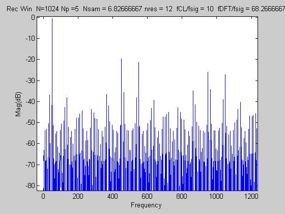
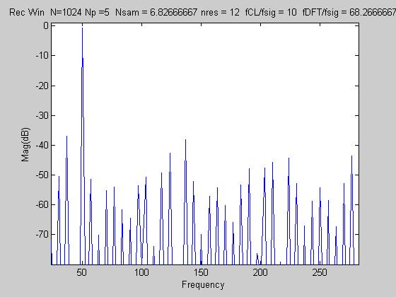
69 Quantization Effects N Q =6, 12 and 24 DFT = 1024
70
71
72
73 Magnitude of Fundamental nd Harmonic in db Res 12 No. points 1024 fsig = No.DFT Periods 5.00 No Sig Periods fcl/fsig Nsamp = 6.83 Rectangular Window Pyyt = Columns 1 through Columns 8 through Columns 15 through
74 Columns 22 through Columns 29 through Columns 36 through Columns 43 through Columns 50 through Columns 57 through
75 Columns 64 through Columns 71 through Columns 78 through Columns 85 through Columns 92 through Columns 99 through
76
77
78
79 Magnitude of Fundamental nd Harmonic in db Res 24 No. points 1024 fsig = No.DFT Periods 5.00 No Sig Periods fcl/fsig Nsamp = 6.83 Rectangular Window Pyyt = Columns 1 through Columns 8 through Columns 15 through Columns 22 through
80 Columns 29 through Columns 36 through Columns 43 through Columns 50 through Columns 57 through Columns 64 through
81 Columns 71 through Columns 78 through Columns 85 through Columns 92 through Columns 99 through Columns 106 through
82
83
84
85 Magnitude of Fundamental nd Harmonic in db Res 6 No. points 1024 fsig = No.DFT Periods 5.00 No Sig Periods fcl/fsig Nsamp = 6.83 Rectangular Window Pyyt = Columns 1 through Columns 8 through Columns 15 through Columns 22 through
86 Columns 29 through Columns 36 through Columns 43 through Columns 50 through Columns 57 through Columns 64 through
87 Columns 71 through Columns 78 through Columns 85 through Columns 92 through Columns 99 through Columns 106 through
88 DAC Comparisons with Quantization N θ Nsam n A 1 A 2 A 3 32K K
89 Comparison of DAC resolution levels 12-bit resolution DFT = bit resolution 24-bit resolution
90 Quantization Effects N Q =6, 12 and 14 DFT = 16,384
91
92
93
94
95 Rectangular Window Pyyt = Columns 1 through Columns 8 through Columns 15 through Columns 22 through Columns 29 through
96 Columns 36 through Columns 43 through Columns 50 through Columns 57 through Columns 64 through Columns 71 through
97 Columns 78 through Columns 85 through Columns 92 through Columns 99 through Columns 106 through
98
99
100
101
102 Res 24 No. points fsig = No.DFT Periods 5.00 No Sig Periods fcl/fsig Nsamp = Rectangular Window Pyyt = Columns 1 through Columns 8 through Columns 15 through Columns 22 through
103 Columns 29 through Columns 36 through Columns 43 through Columns 50 through Columns 57 through Columns 64 through
104 Columns 71 through Columns 78 through Columns 85 through Columns 92 through Columns 99 through Columns 106 through
105
106
107
108
109 Res 6 No. points fsig = No.DFT Periods 5.00 No Sig Periods fcl/fsig Nsamp = Rectangular Window Pyyt = Columns 1 through Columns 8 through Columns 15 through Columns 22 through
110 Columns 29 through Columns 36 through Columns 43 through Columns 50 through Columns 57 through Columns 64 through
111 Columns 71 through Columns 78 through Columns 85 through Columns 92 through Columns 99 through Columns 106 through
112 Comparison of DAC resolution levels DFT = 16, bit resolution 24-bit resolution 12-bit resolution
113 Comparison of DAC resolution levels DFT = 16, bit resolution 24-bit resolution 12-bit resolution
114 DAC Comparisons with Quantization N θ Nsam n A 1 A 2 A 3 32K K K K K
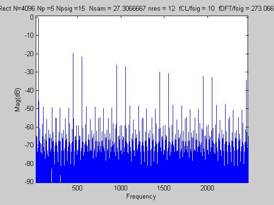
115 DFT Length Effects DFT = 8,10,12, 14, and 16 bits
116
117
118 Res 18 No. points 256 fsig = No.DFT Periods 5.00 No Sig Periods fcl/fsig Nsamp = 1.71 Rectangular Window Pyyt = Columns 1 through Columns 8 through Columns 15 through Columns 22 through
119 Columns 29 through Columns 36 through Columns 43 through Columns 50 through Columns 57 through Columns 64 through
120 Columns 29 through Columns 36 through Columns 43 through Columns 50 through Columns 57 through Columns 64 through
121
122
123
124 Res 18 No. points 1024 fsig = No.DFT Periods 5.00 No Sig Periods fcl/fsig Nsamp = 6.83 Rectangular Window Pyyt = Columns 1 through Columns 8 through Columns 15 through Columns 22 through
125 Columns 29 through Columns 36 through Columns 43 through Columns 50 through Columns 57 through Columns 64 through
126
127
128
129 Res 18 No. points 4096 fsig = No.DFT Periods 5.00 No Sig Periods fcl/fsig Nsamp = Rectangular Window Pyyt = Columns 1 through Columns 8 through Columns 15 through Columns 22 through
130 Columns 29 through Columns 36 through Columns 43 through Columns 50 through Columns 57 through Columns 64 through
131
132
133
134
135 Res 18 No. points fsig = No.DFT Periods 5.00 No Sig Periods fcl/fsig Nsamp = Rectangular Window Pyyt = Columns 1 through Columns 8 through Columns 15 through Columns 22 through
136
137
138
139
140 Magnitude of Fundamental nd Harmonic in db Res 18 No. points fsig = No.DFT Periods 5.00 No Sig Periods fcl/fsig Nsamp = Rectangular Window Pyyt = Columns 1 through Columns 8 through Columns 15 through Columns 22 through
141 Columns 29 through Columns 36 through Columns 43 through Columns 50 through Columns 57 through Columns 64 through
142 DFT Length Effects
143 DFT Length Effects
144 Comparison of DAC Resolution Levels Resolutions: = 4,6,8,10,12, 14, and 16 bits
145
146
147
148 Res 4 No. points 4096 fsig = No.DFT Periods 5.00 No Sig Periods fcl/fsig Nsamp = Rectangular Window Pyyt = Columns 1 through Columns 8 through Columns 15 through Columns 22 through Columns 29 through 35
149
150
151
152 Res 6 No. points 4096 fsig = No.DFT Periods 5.00 No Sig Periods fcl/fsig Nsamp = Rectangular Window Pyyt = Columns 1 through Columns 8 through Columns 15 through Columns 22 through Columns 29 through 35
153
154
155
156 Res 8 No. points 4096 fsig = No.DFT Periods 5.00 No Sig Periods fcl/fsig Nsamp = Rectangular Window Pyyt = Columns 1 through Columns 8 through Columns 15 through Columns 22 through Columns 29 through 35
157
158
159
160 Res 10 No. points 4096 fsig = No.DFT Periods 5.00 No Sig Periods fcl/fsig Nsamp = Rectangular Window Pyyt = Columns 1 through Columns 8 through Columns 15 through Columns 22 through
161
162
163
164 Res 12 No. points 4096 fsig = No.DFT Periods 5.00 No Sig Periods fcl/fsig Nsamp = Rectangular Window Pyyt = Columns 1 through Columns 8 through Columns 15 through Columns 22 through Columns 29 through 35
165
166
167
168 Columns 29 through 35 Res 14 No. points 4096 fsig = No.DFT Periods 5.00 No Sig Periods fcl/fsig Nsamp = Rectangular Window Pyyt = Columns 1 through Columns 8 through Columns 15 through Columns 22 through
169
170
171
172 Res 16 No. points 4096 fsig = No.DFT Periods 5.00 No Sig Periods fcl/fsig Nsamp = Rectangular Window Pyyt = Columns 1 through Columns 8 through Columns 15 through Columns 22 through
173 Comparison of DAC Resolution Levels
174 Comparison of DAC Resolution Levels
175 DAC Comparisons with Quantization N θ Nsam n A 1 A 2 A 3 32K K K K K K
176
177
178
179 Res 12 No. points fsig = No.DFT Periods 1.00 No Sig Periods 1.00 fcl/fsig Nsamp = Rectangular Window Pyyt = Columns 1 through Columns 8 through Columns 15 through Columns 22 through
180
181
182
183 Res 16 No. points 4096 fsig = No.DFT Periods No Sig Periods fcl/fsig Nsamp = Rectangular Window Pyyt = Columns 1 through Columns 8 through Columns 15 through Columns 22 through
184
185
186
187 Res 16 No. points 4096 fsig = No.DFT Periods No Sig Periods fcl/fsig Nsamp = 6.95 Rectangular Window Pyyt = Columns 1 through Columns 8 through Columns 15 through Columns 22 through
188
189
190
191 Res 16 No. points 4096 fsig = No.DFT Periods 5.00 No Sig Periods fcl/fsig Nsamp = Rectangular Window Pyyt = Columns 1 through Columns 8 through Columns 15 through Columns 22 through
192
193
194
195 Res 16 No. points 4096 fsig = No.DFT Periods 3.00 No Sig Periods 9.00 fcl/fsig Nsamp = 4.55 Rectangular Window Pyyt = Columns 1 through Columns 8 through Columns 15 through Columns 22 through Columns 29 through 35
196
197
198
199 Res 16 No. points 4096 fsig = No.DFT Periods 1.00 No Sig Periods 3.00 fcl/fsig Nsamp = Rectangular Window Pyyt = Columns 1 through Columns 8 through Columns 15 through Columns 22 through Columns 29 through 35
200 End Skip
201 Summary of time and amplitude quantization assessment Time and amplitude quantization do not introduce harmonic distortion Time and amplitude quantization do increase the noise floor
202 Duty Cycle Effects on Spectral Performance of DACS File: DAC Quantization with RTZ.m
203 Consider N P =1 N SIG =11 N CL =70 f sig =50 n res =10 Thus, f CLK =f SIG (N CL /N SIG )=318Hz The fft spectrum should be nominally symmetric around f CLK /2=159Hz so will get only the fundamental, second harmonic, and third harmonic in the fundamental frequency half-period which occurs at fft coefficient number 36 and the clock frequency will be at fft coefficient number 71 (and thus the fundamental will appear at fft coefficient numbers 11+1=12 and 71-11=60) The relationship between fft coefficient number and frequency is given by n-1 f= f NSIG SIG or by n=1+f N f SIG SIG
204
205
206
207
208 Magnitude of Fundamental nd Harmonic in db Res 10 No. points fsig = No.DFT Periods 1.00 No Sig Periods fcl/fsig 6.36 Nsamp = DutyCycle = 1.0 Rectangular Window Pyyt = Columns 1 through Columns 9 through Columns 17 through
209 Columns 25 through Columns 33 through Columns 41 through Columns 49 through Columns 57 through Columns 65 through
210 Columns 73 through Columns 81 through Columns 89 through Columns 97 through Columns 105 through

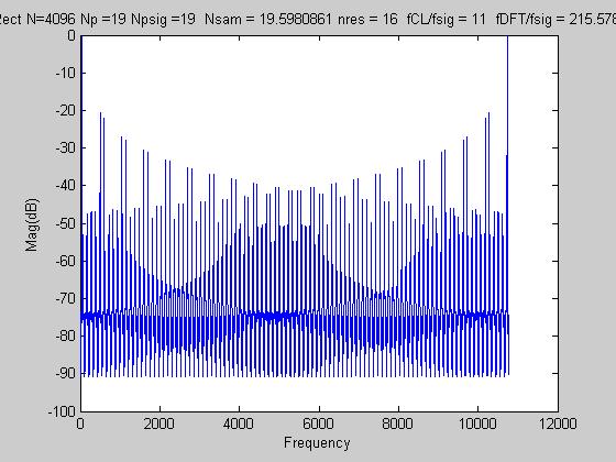
211
212
213
214
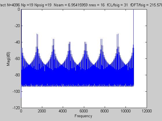
215 Magnitude of Fundamental nd Harmonic in db Res 10 No. points fsig = No.DFT Periods 1.00 No Sig Periods 11.0 fcl/fsig 6.36 Nsamp = DutyCycle = 0.5 Rectangular Window Columns 1 through Columns 9 through Columns 17 through Columns 25 through
216 Columns 33 through Columns 41 through Columns 49 through Columns 57 through Columns 65 through Columns 73 through
217 Columns 81 through Columns 89 through Columns 97 through Columns 105 through
218 DAC Comparisons with Quantization N θ Nsam n A 1 A 2 A 3 32K K K K K K K K
219 Summary of Duty Cycle Effects Duty Cycle does dot introduce harmonic distortion Duty Cycle reduction reduces signal levels thus degrades SNR
220 Number of Samples/Period One Sample per Period Multiple Samples per Period Many authors use a data acquisition system and select one sample/period Spectrum analyzer will generally measure continuous-time effects
221 Number of Samples/Period Nonlinear Settling Glitch Glitch Typical DAC Response
222 Number of Samples/Period Incorrect Settling Typical DAC Response
223 Number of Samples/Period Incorrect Settling Settling error can be multiple LSB at Nyquist Rate Multiple LSB settling error does not cause distortion if settling is linear Glitches are a significant contributor to spectral distortion (at high frequencies)
224 Typical SFDR Plot From: Y. Cong and R. L. Geiger, "A 1.5-v 14-bit 100-MS/s Self-Calibrated DAC," IEEE J. of Solid State Circuits, December 2003, vol. 38, no. 12, pp
225 Spectral Characterization of Data Converters Distortion Analysis Time Quantization Effects of DACs of ADCs Amplitude Quantization Effects of DACs of ADCs Clock Jitter
226 Effects of Jitter on Spectral Performance
227 Model of Jitter T S Ideal Clock Jittery Clock t Jk Assume t Jk are uncorrelated uniformly distributed random variables θ θ tjk U - T S, TS 2 2 Note: there can also be jitter in the ideal clock or there may be no ideal clock so zero crossings may be modeled as a random walk or a sum of a random walk and uniform jitter. Analysis more complicated in these cases.
228 Model of Jitter Assume t Jk are uncorrelated uniformly distributed random variables θ θ tjk U - T S, TS 2 2 Consider θ=.01,.001,.0001, Observe: If T S is a 100MHz clock, then T S =10nsec and θ=.0001 corresponds to 1psec (±0.5psec) of symmetric jitter
229
230
231
232
233 Statistical Characterization of Electronic Components and Circuits Recall: Almost all data converter structures work perfectly if components are ideal Major challenges in data converter design Parasitic Resistances and Capacitances Nonlinearity in components Statistical variation in components and circuits Model uncertainties Power supply variability
234 Consider a flash ADC V REF V IN R R R R Thermometer to Binary Decoder n X OUT Resistor values and offset voltages of Comparators are all random variables at design level Variations of these RVs affect the break point and thus the yield R
235 Consider Current-Steering DAC V DD I 1 I 1 /2 I 1 /4 I 1 /8 b 3 b 2 b 1 b 0 R F V OUT Ideally n -1 b i OUT 1 F n-i i=0 2 V = -I R
236 Consider Current-Steering DAC V DD V DD M REF M n-1 M 1 M 0 I 1 I 1 /2 I 1 /4 I 1 /8 b 3 b 2 b 1 b 0 R F V R I n-1 I 1 I 0 V OUT I REF b n-1 M (n-1)s M 1S b0 b 1 M 0S Basic Implementation of Current Sources Ideally Actually I μc W V -V 2 OX k k R Tp 2 L k L k=l0 k-1 W k=2 W0 I μc W V -V 2 k OXk k k R Tpk 2 L k I k is a random variables and is a function of the model parameters μ k, C OXk, W k, L k, and V Tpk μ k, C OXk, W k, L k, and V Tpk are all random variables
237 Recall from previous lecture How important is statistical analysis? Example: 7-bit FLASH ADC with R-string DAC V REF V IN Assume R-string is ideal, V REF =1V and V OS for each comparator must be at most +/- ½ LSB Case 1 Standard deviation is 5mV Case 2 P COMP = Y = ADC -32 R R R R Thermometer to Binary Decoder n X OUT Standard deviation is 1mV P COMP Y =0.988 ADC R Statistics play a key role in the performance and consequently yield of a data converter
238 End of Lecture 7
EE 505 Lecture 10. Spectral Characterization. Part 2 of 2
 EE 505 Lecture 10 Spectral Characterization Part 2 of 2 Review from last lecture Spectral Analysis If f(t) is periodic f(t) alternately f(t) = = A A ( kω t + ) 0 + Aksin θk k= 1 0 + a ksin t k= 1 k= 1
Distortion Analysis T
 EE 435 Lecture 32 Spectral Performance Windowing Spectral Performance of Data Converters - Time Quantization - Amplitude Quantization Quantization Noise . Review from last lecture. Distortion Analysis
EE 435. Lecture 32. Spectral Performance Windowing
 EE 435 Lecture 32 Spectral Performance Windowing . Review from last lecture. Distortion Analysis T 0 T S THEOREM?: If N P is an integer and x(t) is band limited to f MAX, then 2 Am Χ mnp 1 0 m h N and
EE 505 Lecture 8. Clock Jitter Statistical Circuit Modeling
 EE 505 Lecture 8 Clock Jitter Statistical Circuit Modeling Spectral Characterization of Data Converters Distortion Analysis Time Quantization Effects of DACs of ADCs Amplitude Quantization Effects of DACs
EE 435. Lecture 26. Data Converters. Data Converter Characterization
 EE 435 Lecture 26 Data Converters Data Converter Characterization . Review from last lecture. Data Converter Architectures Large number of different circuits have been proposed for building data converters
EE 230 Lecture 40. Data Converters. Amplitude Quantization. Quantization Noise
 EE 230 Lecture 40 Data Converters Amplitude Quantization Quantization Noise Review from Last Time: Time Quantization Typical ADC Environment Review from Last Time: Time Quantization Analog Signal Reconstruction
EE 435. Lecture 28. Data Converters Linearity INL/DNL Spectral Performance
 EE 435 Lecture 8 Data Converters Linearity INL/DNL Spectral Performance Performance Characterization of Data Converters Static characteristics Resolution Least Significant Bit (LSB) Offset and Gain Errors
EE 230 Lecture 43. Data Converters
 EE 230 Lecture 43 Data Converters Review from Last Time: Amplitude Quantization Unwanted signals in the output of a system are called noise. Distortion Smooth nonlinearities Frequency attenuation Large
EE247 Lecture 16. Serial Charge Redistribution DAC
 EE47 Lecture 16 D/A Converters D/A examples Serial charge redistribution DAC Practical aspects of current-switch DACs Segmented current-switch DACs DAC self calibration techniques Current copiers Dynamic
EE 435. Lecture 26. Data Converters. Data Converter Characterization
 EE 435 Lecture 26 Data Converters Data Converter Characterization . Review from last lecture. Data Converter Architectures n DAC R-2R (4-bits) R R R R V OUT 2R 2R 2R 2R R d 3 d 2 d 1 d 0 V REF By superposition:
Data Converter Fundamentals
 Data Converter Fundamentals David Johns and Ken Martin (johns@eecg.toronto.edu) (martin@eecg.toronto.edu) slide 1 of 33 Introduction Two main types of converters Nyquist-Rate Converters Generate output
Lecture 340 Characterization of DACs and Current Scaling DACs (5/1/10) Page 340-1
 Page 340-1") Lecture 34 Characterization of DACs and Current Scaling DACs (5//) Page 34 LECTURE 34 CHARACTERZATON OF DACS AND CURRENT SCALNG DACS LECTURE ORGANZATON Outline ntroduction Static characterization of DACs
Lecture 34 Characterization of DACs and Current Scaling DACs (5//) Page 34 LECTURE 34 CHARACTERZATON OF DACS AND CURRENT SCALNG DACS LECTURE ORGANZATON Outline ntroduction Static characterization of DACs
EE 435. Lecture 36. Quantization Noise ENOB Absolute and Relative Accuracy DAC Design. The String DAC
 EE 435 Lecture 36 Quantization Noise ENOB Absolute and elative Accuracy DAC Design The String DAC . eview from last lecture. Quantization Noise in ADC ecall: If the random variable f is uniformly distributed
EE 435. Lecture 30. Data Converters. Spectral Performance
 EE 435 Lecture 30 Data Converters Spectral Performance . Review from last lecture. INL Often Not a Good Measure of Linearity Four identical INL with dramatically different linearity X OUT X OUT X REF X
EE 435. Lecture 29. Data Converters. Linearity Measures Spectral Performance
 EE 435 Lecture 9 Data Converters Linearity Measures Spectral Performance Linearity Measurements (testing) Consider ADC V IN (t) DUT X IOUT V REF Linearity testing often based upon code density testing
D/A Converters. D/A Examples
 D/A architecture examples Unit element Binary weighted Static performance Component matching Architectures Unit element Binary weighted Segmented Dynamic element matching Dynamic performance Glitches Reconstruction
Lecture 10, ATIK. Data converters 3
 Lecture, ATIK Data converters 3 What did we do last time? A quick glance at sigma-delta modulators Understanding how the noise is shaped to higher frequencies DACs A case study of the current-steering
EEO 401 Digital Signal Processing Prof. Mark Fowler
 EEO 401 Digital Signal Processing Pro. Mark Fowler Note Set #14 Practical A-to-D Converters and D-to-A Converters Reading Assignment: Sect. 6.3 o Proakis & Manolakis 1/19 The irst step was to see that
Summary Last Lecture
 EE247 Lecture 19 ADC Converters Sampling (continued) Sampling switch charge injection & clock feedthrough Complementary switch Use of dummy device Bottom-plate switching Track & hold T/H circuits T/H combined
ELEN 610 Data Converters
 Spring 04 S. Hoyos - EEN-60 ELEN 60 Data onverters Sebastian Hoyos Texas A&M University Analog and Mixed Signal Group Spring 04 S. Hoyos - EEN-60 Electronic Noise Signal to Noise ratio SNR Signal Power
EE 435. Lecture 26. Data Converters. Differential Nonlinearity Spectral Performance
 EE 435 Lecture 26 Data Converters Differential Nonlinearity Spectral Performance . Review from last lecture. Integral Nonlinearity (DAC) Nonideal DAC INL often expressed in LSB INL = X k INL= max OUT OF
EE 435. Lecture 38. DAC Design Current Steering DACs Charge Redistribution DACs ADC Design
 EE 435 Lecture 38 DAC Design Current Steering DACs Charge edistribution DACs ADC Design eview from last lecture Current Steering DACs X N Binary to Thermometer ndecoder (all ON) S S N- S N V EF F nherently
A novel Capacitor Array based Digital to Analog Converter
 Chapter 4 A novel Capacitor Array based Digital to Analog Converter We present a novel capacitor array digital to analog converter(dac architecture. This DAC architecture replaces the large MSB (Most Significant
Digital to Analog Converters I
 Advanced Analog Building Blocks 2 Digital to Analog Converters I Albert Comerma (PI) (comerma@physi.uni-heidelberg.de) Course web WiSe 2017 DAC parameters DACs parameters DACs non ideal effects DACs performance
EE 505 Lecture 11. Statistical Circuit Modeling. R-string Example Offset Voltages
 EE 505 Lecture 11 Statistical Circuit Modeling -string Example Offset oltages eview from previous lecture: Current Steering DAC Statistical Characterization Binary Weighted IL b= 1 1 IGk 1 1 I
EE 521: Instrumentation and Measurements
 Aly El-Osery Electrical Engineering Department, New Mexico Tech Socorro, New Mexico, USA September 23, 2009 1 / 18 1 Sampling 2 Quantization 3 Digital-to-Analog Converter 4 Analog-to-Digital Converter
Nyquist-Rate D/A Converters. D/A Converter Basics.
 Nyquist-Rate D/A Converters David Johns and Ken Martin (johns@eecg.toronto.edu) (martin@eecg.toronto.edu) slide 1 of 20 D/A Converter Basics. B in D/A is a digital signal (or word), B in b i B in = 2 1
EE 505. Lecture 27. ADC Design Pipeline
 EE 505 Lecture 7 AD Design Pipeline Review Sampling Noise V n5 R S5 dv REF V n4 R S4 V ns V ns β= + If the ON impedance of the switches is small and it is assumed that = =, it can be shown that Vˆ IN-RMS
Slide Set Data Converters. Digital Enhancement Techniques
 0 Slide Set Data Converters Digital Enhancement Techniques Introduction Summary Error Measurement Trimming of Elements Foreground Calibration Background Calibration Dynamic Matching Decimation and Interpolation
Successive Approximation ADCs
 Department of Electrical and Computer Engineering Successive Approximation ADCs Vishal Saxena Vishal Saxena -1- Successive Approximation ADC Vishal Saxena -2- Data Converter Architectures Resolution [Bits]
Sistemas de Aquisição de Dados. Mestrado Integrado em Eng. Física Tecnológica 2016/17 Aula 3, 3rd September
 Sistemas de Aquisição de Dados Mestrado Integrado em Eng. Física Tecnológica 2016/17 Aula 3, 3rd September The Data Converter Interface Analog Media and Transducers Signal Conditioning Signal Conditioning
Lecture 4, Noise. Noise and distortion
 Lecture 4, Noise Noise and distortion What did we do last time? Operational amplifiers Circuit-level aspects Simulation aspects Some terminology Some practical concerns Limited current Limited bandwidth
Switched-Capacitor Circuits David Johns and Ken Martin University of Toronto
 Switched-Capacitor Circuits David Johns and Ken Martin University of Toronto (johns@eecg.toronto.edu) (martin@eecg.toronto.edu) University of Toronto 1 of 60 Basic Building Blocks Opamps Ideal opamps usually
An Efficient Bottom-Up Extraction Approach to Build the Behavioral Model of Switched-Capacitor. ΔΣ Modulator. Electronic Design Automation Laboratory
 Electronic Design Automation Laboratory National Central University Department of Electrical Engineering, Taiwan ( R.O.C) An Efficient Bottom-Up Extraction Approach to Build the Behavioral Model of Switched-Capacitor
ECEN 610 Mixed-Signal Interfaces
 ECEN 610 Mixed-Signal Interfaces Sebastian Hoyos Texas A&M University Analog and Mixed Signal Group Spring 014 S. Hoyos-ECEN-610 1 Sample-and-Hold Spring 014 S. Hoyos-ECEN-610 ZOH vs. Track-and-Hold V(t)
PARALLEL DIGITAL-ANALOG CONVERTERS
 CMOS Analog IC Design Page 10.2-1 10.2 - PARALLEL DIGITAL-ANALOG CONVERTERS CLASSIFICATION OF DIGITAL-ANALOG CONVERTERS CMOS Analog IC Design Page 10.2-2 CURRENT SCALING DIGITAL-ANALOG CONVERTERS GENERAL
Analog to Digital Converters (ADCs)
") Analog to Digital Converters (ADCs) Note: Figures are copyrighted Proakis & Manolakis, Digital Signal Processing, 4 th Edition, Pearson Publishers. Embedded System Design A Unified HW Approach, Vahid/Givargis,
Analog to Digital Converters (ADCs) Note: Figures are copyrighted Proakis & Manolakis, Digital Signal Processing, 4 th Edition, Pearson Publishers. Embedded System Design A Unified HW Approach, Vahid/Givargis,
Oversampling Converters
 Oversampling Converters David Johns and Ken Martin (johns@eecg.toronto.edu) (martin@eecg.toronto.edu) slide 1 of 56 Motivation Popular approach for medium-to-low speed A/D and D/A applications requiring
Research Article Linearity Analysis on a Series-Split Capacitor Array for High-Speed SAR ADCs
 Hindawi Publishing Corporation LSI Design olume 1, Article ID 76548, 8 pages doi:1.1155/1/76548 Research Article Linearity Analysis on a Series-Split Capacitor Array for High-Speed SAR ADCs Yan Zhu, 1
EE 5345 Biomedical Instrumentation Lecture 12: slides
 EE 5345 Biomedical Instrumentation Lecture 1: slides 4-6 Carlos E. Davila, Electrical Engineering Dept. Southern Methodist University slides can be viewed at: http:// www.seas.smu.edu/~cd/ee5345.html EE
Nyquist-Rate A/D Converters
 IsLab Analog Integrated ircuit Design AD-51 Nyquist-ate A/D onverters כ Kyungpook National University IsLab Analog Integrated ircuit Design AD-1 Nyquist-ate MOS A/D onverters Nyquist-rate : oversampling
Simulation of the Effects of Timing Jitter in Track-and-Hold and Sample-and-Hold Circuits
 5. Simulation of the Effects of Timing Jitter in Track-and-Hold and Sample-and-Hold Circuits V. Vasudevan Department of Electrical Engineering Indian Institute of Technology-Madras Chennai-636, India Email:
DEPARTMENT OF INFORMATION AND COMMUNICATION TECHNOLOGY
 UNIVERSITY OF TRENTO DEPARTMENT OF INFORMATION AND COMMUNICATION TECHNOLOGY 38050 Povo Trento Italy, Via Sommarive 14 http://www.dit.unitn.it A RISKS ASSESSMENT AND CONFORMANCE TESTING OF ANALOG-TO-DIGITAL
EE 505. Lecture 29. ADC Design. Oversampled
 EE 505 Lecture 29 ADC Desig Oversampled Review from Last Lecture SAR ADC V IN Sample Hold C LK V REF DAC DAC Cotroller DAC Cotroller stores estimates of iput i Successive Approximatio Register (SAR) At
Q. 1 Q. 25 carry one mark each.
 GATE 5 SET- ELECTRONICS AND COMMUNICATION ENGINEERING - EC Q. Q. 5 carry one mark each. Q. The bilateral Laplace transform of a function is if a t b f() t = otherwise (A) a b s (B) s e ( a b) s (C) e as
J.-M Friedt. FEMTO-ST/time & frequency department. slides and references at jmfriedt.free.fr.
 FEMTO-ST/time & frequency department jmfriedt@femto-st.fr slides and references at jmfriedt.free.fr February 21, 2018 1 / 17 Basics ADC: discrete time (aliasing) and discrete levels (quantization) V =
EXAMPLE DESIGN PART 2
 ECE37 Advanced Analog Circuits Lecture 3 EXAMPLE DESIGN PART 2 Richard Schreier richard.schreier@analog.com Trevor Caldwell trevor.caldwell@utoronto.ca Course Goals Deepen understanding of CMOS analog
Digital Signal Processing
 COMP ENG 4TL4: Digital Signal Processing Notes for Lecture #3 Wednesday, September 10, 2003 1.4 Quantization Digital systems can only represent sample amplitudes with a finite set of prescribed values,
EE 505 Lecture 10. Statistical Circuit Modeling
 EE 505 Lecture 10 Statistical Circuit Modeling Amplifier Gain Accuracy eview from previous lecture: - + String DAC Statistical Performance eview from previous lecture: esistors are uncorrelated but identically
An Anti-Aliasing Multi-Rate Σ Modulator
 An Anti-Aliasing Multi-Rate Σ Modulator Anthony Chan Carusone Depart. of Elec. and Comp. Eng. University of Toronto, Canada Franco Maloberti Department of Electronics University of Pavia, Italy May 6,
Measurement and Instrumentation. Sampling, Digital Devices, and Data Acquisition
 2141-375 Measurement and Instrumentation Sampling, Digital Devices, and Data Acquisition Basic Data Acquisition System Analog Form Analog Form Digital Form Display Physical varialble Sensor Signal conditioning
Analog and Telecommunication Electronics
 Politecnico di Torino Electronic Eng. Master Degree Analog and Telecommunication Electronics D2 - DAC taxonomy and errors» Static and dynamic parameters» DAC taxonomy» DAC circuits» Error sources AY 2015-16
Lecture 6, ATIK. Switched-capacitor circuits 2 S/H, Some nonideal effects Continuous-time filters
 Lecture 6, ATIK Switched-capacitor circuits 2 S/H, Some nonideal effects Continuous-time filters What did we do last time? Switched capacitor circuits The basics Charge-redistribution analysis Nonidealties
EXAMPLE DESIGN PART 2
 ECE37 Advanced Analog Circuits Lecture 4 EXAMPLE DESIGN PART 2 Richard Schreier richard.schreier@analog.com Trevor Caldwell trevor.caldwell@utoronto.ca Course Goals Deepen understanding of CMOS analog
EE247 Lecture 19. EECS 247 Lecture 19: Data Converters 2006 H.K. Page 1. Summary Last Lecture
 EE247 Lecture 19 ADC Converters Sampling (continued) Clock boosters (continued) Sampling switch charge injection & clock feedthrough Complementary switch Use of dummy device Bottom-plate switching Track
A Gray Code Based Time-to-Digital Converter Architecture and its FPGA Implementation
 A Gray Code Based Time-to-Digital Converter Architecture and its FPGA Implementation Congbing Li Haruo Kobayashi Gunma University Gunma University Kobayashi Lab Outline Research Objective & Background
Top-Down Design of a xdsl 14-bit 4MS/s Σ Modulator in Digital CMOS Technology
 Top-Down Design of a xdsl -bit 4MS/s Σ Modulator in Digital CMOS Technology R. del Río, J.M. de la Rosa, F. Medeiro, B. Pérez-Verdú, and A. Rodríguez-Vázquez Instituto de Microelectrónica de Sevilla CNM-CSIC
Analog Digital Sampling & Discrete Time Discrete Values & Noise Digital-to-Analog Conversion Analog-to-Digital Conversion
 Analog Digital Sampling & Discrete Time Discrete Values & Noise Digital-to-Analog Conversion Analog-to-Digital Conversion 6.082 Fall 2006 Analog Digital, Slide Plan: Mixed Signal Architecture volts bits
A Nonuniform Quantization Scheme for High Speed SAR ADC Architecture
 A Nonuniform Quantization Scheme for High Speed SAR ADC Architecture Youngchun Kim Electrical and Computer Engineering The University of Texas Wenjuan Guo Intel Corporation Ahmed H Tewfik Electrical and
ETSF15 Analog/Digital. Stefan Höst
 ETSF15 Analog/Digital Stefan Höst Physical layer Analog vs digital Sampling, quantisation, reconstruction Modulation Represent digital data in a continuous world Disturbances Noise and distortion Synchronization
Correlation, discrete Fourier transforms and the power spectral density
 Correlation, discrete Fourier transforms and the power spectral density visuals to accompany lectures, notes and m-files by Tak Igusa tigusa@jhu.edu Department of Civil Engineering Johns Hopkins University
Seminar: D. Jeon, Energy-efficient Digital Signal Processing Hardware Design Mon Sept 22, 9:30-11:30am in 3316 EECS
 EECS 452 Lecture 6 Today: Announcements: Rounding and quantization Analog to digital conversion Lab 3 starts next week Hw3 due on tuesday Project teaming meeting: today 7-9PM, Dow 3150 My new office hours:
Slide Set Data Converters. Background Elements
 0 Slide Set Data Converters Background Elements 1 Introduction Summary The Ideal Data Converter Sampling Amplitude Quantization Quantization Noise kt/c Noise Discrete and Fast Fourier Transforms The D/A
Signal types. Signal characteristics: RMS, power, db Probability Density Function (PDF). Analogue-to-Digital Conversion (ADC).
. Analogue-to-Digital Conversion (ADC).") Signal types. Signal characteristics:, power, db Probability Density Function (PDF). Analogue-to-Digital Conversion (ADC). Signal types Stationary (average properties don t vary with time) Deterministic
Signal types. Signal characteristics:, power, db Probability Density Function (PDF). Analogue-to-Digital Conversion (ADC). Signal types Stationary (average properties don t vary with time) Deterministic
INTRODUCTION TO DELTA-SIGMA ADCS
 ECE37 Advanced Analog Circuits INTRODUCTION TO DELTA-SIGMA ADCS Richard Schreier richard.schreier@analog.com NLCOTD: Level Translator VDD > VDD2, e.g. 3-V logic? -V logic VDD < VDD2, e.g. -V logic? 3-V
Lecture 5b: Line Codes
 Lecture 5b: Line Codes Dr. Mohammed Hawa Electrical Engineering Department University of Jordan EE421: Communications I Digitization Sampling (discrete analog signal). Quantization (quantized discrete
EE 505 Lecture 10. Statistical Circuit Modeling
 EE 505 Lecture 10 Statistical Circuit Modeling mplifier Gain ccuracy eview from previous lecture: - + eview from previous lecture: String DC Statistical Performance 1 1 k k k ILk j 1 j 1 k 1 OM j1 1 1
EE 435 Lecture 44. Switched-Capacitor Amplifiers Other Integrated Filters
 EE 435 Lecture 44 Switched-Capacitor Amplifiers Other Integrated Filters Switched-Capacitor Amplifiers Noninverting Amplifier Inverting Amplifier C A V = C C A V = - C Accurate control of gain is possible
High-Speed, High-Resolution, Radiation-Tolerant SAR ADC for Particle Physics Experiments
 Erik Jonsson School of Engineering & Computer Science High-Speed, High-Resolution, Radiation-Tolerant SAR ADC for Particle Physics Experiments Yun Chiu Erik Jonsson Distinguished Professor Texas Analog
2. SPECTRAL ANALYSIS APPLIED TO STOCHASTIC PROCESSES
 2. SPECTRAL ANALYSIS APPLIED TO STOCHASTIC PROCESSES 2.0 THEOREM OF WIENER- KHINTCHINE An important technique in the study of deterministic signals consists in using harmonic functions to gain the spectral
A Modeling Environment for the Simulation and Design of Charge Redistribution DACs Used in SAR ADCs
 204 UKSim-AMSS 6th International Conference on Computer Modelling and Simulation A Modeling Environment for the Simulation and Design of Charge Redistribution DACs Used in SAR ADCs Stefano Brenna, Andrea
Topic 7. Convolution, Filters, Correlation, Representation. Bryan Pardo, 2008, Northwestern University EECS 352: Machine Perception of Music and Audio
 Topic 7 Convolution, Filters, Correlation, Representation Short time Fourier Transform Break signal into windows Calculate DFT of each window The Spectrogram spectrogram(y,1024,512,1024,fs,'yaxis'); A
INTRODUCTION TO DELTA-SIGMA ADCS
 ECE1371 Advanced Analog Circuits Lecture 1 INTRODUCTION TO DELTA-SIGMA ADCS Richard Schreier richard.schreier@analog.com Trevor Caldwell trevor.caldwell@utoronto.ca Course Goals Deepen understanding of
Modeling All-MOS Log-Domain Σ A/D Converters
 DCIS 04 Modeling All-MOS Log Σ ADCs Intro Circuits Modeling Example Conclusions 1/22 Modeling All-MOS Log-Domain Σ A/D Converters X.Redondo 1, J.Pallarès 2 and F.Serra-Graells 1 1 Institut de Microelectrònica
The Linear-Feedback Shift Register
 EECS 141 S02 Timing Project 2: A Random Number Generator R R R S 0 S 1 S 2 1 0 0 0 1 0 1 0 1 1 1 0 1 1 1 0 1 1 0 0 1 1 0 0 The Linear-Feedback Shift Register 1 Project Goal Design a 4-bit LFSR SPEED, SPEED,
EE 435. Lecture 16. Compensation Systematic Two-Stage Op Amp Design
 EE 435 Lecture 6 Compensation Systematic Two-Stage Op Amp Design Review from last lecture Review of Basic Concepts Pole Locations and Stability Theorem: A system is stable iff all closed-loop poles lie
The influence of parasitic capacitors on SAR ADC characteristics
 The influence of parasitic capacitors on SAR ADC characteristics DMITRY NORMANOV, DMITRY OSIPOV National Research Nuclear University MEPHI ASIC Lab 59, Moscow, Kashirskoe shosse, 3 RUSSIA simplere@ya.ru
Low-Noise Sigma-Delta Capacitance-to-Digital Converter for Sub-pF Capacitive Sensors with Integrated Dielectric Loss Measurement
 Low-Noise Sigma-Delta Capacitance-to-Digital Converter for Sub-pF Capacitive Sensors with Integrated Dielectric Loss Measurement Markus Bingesser austriamicrosystems AG Rietstrasse 4, 864 Rapperswil, Switzerland
Sistemas de Aquisição de Dados. Mestrado Integrado em Eng. Física Tecnológica 2016/17 Aula 4, 10th October
 Sistemas de Aquisição de Dados Mestrado Integrado em Eng. Física Tecnológica 216/17 Aula 4, 1th October ADC Amplitude Quantization: ADC Digital Output Formats V REF +FS RANGE (SPAN) OR FS ANALOG INPUT
Lecture 310 Open-Loop Comparators (3/28/10) Page 310-1
 Page 310-1") Lecture 310 Open-Loop Comparators (3/28/10) Page 310-1 LECTURE 310 OPEN-LOOP COMPARATORS LECTURE ORGANIZATION Outline Characterization of comparators Dominant pole, open-loop comparators Two-pole, open-loop
Lecture 310 Open-Loop Comparators (3/28/10) Page 310-1 LECTURE 310 OPEN-LOOP COMPARATORS LECTURE ORGANIZATION Outline Characterization of comparators Dominant pole, open-loop comparators Two-pole, open-loop
SWITCHED CAPACITOR AMPLIFIERS
 SWITCHED CAPACITOR AMPLIFIERS AO 0V 4. AO 0V 4.2 i Q AO 0V 4.3 Q AO 0V 4.4 Q i AO 0V 4.5 AO 0V 4.6 i Q AO 0V 4.7 Q AO 0V 4.8 i Q AO 0V 4.9 Simple amplifier First approach: A 0 = infinite. C : V C = V s
Pipelined multi step A/D converters
 Department of Electrical Engineering Indian Institute of Technology, Madras Chennai, 600036, India 04 Nov 2006 Motivation for multi step A/D conversion Flash converters: Area and power consumption increase
Slide Set Data Converters. High-Order, CT Σ Converters and Σ DAC
 0 lide et Data Converters High-Order, CT Σ Converters and Σ DAC 1 NR Enhancement ummary High Order Noise haping Continuos-Time Σ Modulators Band-Pass Σ Modulators Oversampling DAC 2 NR Enhancement Many
Switched-Capacitor Filters
 Switched-Capacitor Filters Analog sampled-data filters: Continuous amplitude Quantized time Applications: Oversampled and D/A converters Analog front-ends (CDS, etc) Standalone filters E.g. National Semiconductor
ELEN E4810: Digital Signal Processing Topic 11: Continuous Signals. 1. Sampling and Reconstruction 2. Quantization
 ELEN E4810: Digital Signal Processing Topic 11: Continuous Signals 1. Sampling and Reconstruction 2. Quantization 1 1. Sampling & Reconstruction DSP must interact with an analog world: A to D D to A x(t)
DSP Configurations. responded with: thus the system function for this filter would be
 DSP Configurations In this lecture we discuss the different physical (or software) configurations that can be used to actually realize or implement DSP functions. Recall that the general form of a DSP
Higher-Order Σ Modulators and the Σ Toolbox
 ECE37 Advanced Analog Circuits Higher-Order Σ Modulators and the Σ Toolbox Richard Schreier richard.schreier@analog.com NLCOTD: Dynamic Flip-Flop Standard CMOS version D CK Q Q Can the circuit be simplified?
Analog and Mixed-Signal Center, TAMU
 Analog and MixedSignal enter, TAMU SampleandHold ircuit S/H: S H S H S H S H S t i S/H circuit o o S/H command i Block Diagram Idealized Response t Performances of S & H Realistic Transient Response: Input
Digital Signal 2 N Most Significant Bit (MSB) Least. Bit (LSB)
 Least. Bit (LSB)") 1 Digital Signal Binary or two stages: 0 (Low voltage 0-3 V) 1 (High voltage 4-5 V) Binary digit is called bit. Group of bits is called word. 8-bit group is called byte. For N-bit base-2 number = 2 N levels
1 Digital Signal Binary or two stages: 0 (Low voltage 0-3 V) 1 (High voltage 4-5 V) Binary digit is called bit. Group of bits is called word. 8-bit group is called byte. For N-bit base-2 number = 2 N levels
ir. Georgi Radulov 1, dr. ir. Patrick Quinn 2, dr. ir. Hans Hegt 1, prof. dr. ir. Arthur van Roermund 1 Eindhoven University of Technology Xilinx
 Calibration of Current Steering D/A Converters ir. eorgi Radulov 1, dr. ir. Patrick Quinn 2, dr. ir. Hans Hegt 1, prof. dr. ir. Arthur van Roermund 1 1 Eindhoven University of Technology 2 Xilinx Current-steering
EE4512 Analog and Digital Communications Chapter 4. Chapter 4 Receiver Design
 Chapter 4 Receiver Design Chapter 4 Receiver Design Probability of Bit Error Pages 124-149 149 Probability of Bit Error The low pass filtered and sampled PAM signal results in an expression for the probability
Lab 3 Revisited. Zener diodes IAP 2008 Lecture 4 1
 Lab 3 Revisited Zener diodes R C 6.091 IAP 2008 Lecture 4 1 Lab 3 Revisited +15 Voltage regulators 555 timers 270 1N758 0.1uf 5K pot V+ V- 2N2222 0.1uf V o. V CC V Vin s = 5 V Vc V c Vs 1 e t = RC Threshold
Correlator I. Basics. Chapter Introduction. 8.2 Digitization Sampling. D. Anish Roshi
 Chapter 8 Correlator I. Basics D. Anish Roshi 8.1 Introduction A radio interferometer measures the mutual coherence function of the electric field due to a given source brightness distribution in the sky.
Lecture 400 Discrete-Time Comparators (4/8/02) Page 400-1
 Page 400-1") Lecture 400 DiscreteTime omparators (4/8/02) Page 4001 LETURE 400 DISRETETIME OMPARATORS (LATHES) (READING: AH 475483) Objective The objective of this presentation is: 1.) Illustrate discretetime comparators
Lecture 400 DiscreteTime omparators (4/8/02) Page 4001 LETURE 400 DISRETETIME OMPARATORS (LATHES) (READING: AH 475483) Objective The objective of this presentation is: 1.) Illustrate discretetime comparators
EE290C Spring Motivation. Lecture 6: Link Performance Analysis. Elad Alon Dept. of EECS. Does eqn. above predict everything? EE290C Lecture 5 2
 EE29C Spring 2 Lecture 6: Link Performance Analysis Elad Alon Dept. of EECS Motivation V in, ampl Voff BER = 2 erfc 2σ noise Does eqn. above predict everything? EE29C Lecture 5 2 Traditional Approach Borrowed
Accurate Fourier Analysis for Circuit Simulators
 Accurate Fourier Analysis for Circuit Simulators Kenneth S. Kundert Cadence Design Systems (Based on Presentation to CICC 94) Abstract A new approach to Fourier analysis within the context of circuit simulation
System on a Chip. Prof. Dr. Michael Kraft
 System on a Chip Prof. Dr. Michael Kraft Lecture 3: Sample and Hold Circuits Switched Capacitor Circuits Circuits and Systems Sampling Signal Processing Sample and Hold Analogue Circuits Switched Capacitor
Voltage-Controlled Oscillator (VCO)
") Voltage-Controlled Oscillator (VCO) Desirable characteristics: Monotonic f osc vs. V C characteristic with adequate frequency range f max f osc Well-defined K vco f min slope = K vco VC V C in V K F(s)
Voltage-Controlled Oscillator (VCO) Desirable characteristics: Monotonic f osc vs. V C characteristic with adequate frequency range f max f osc Well-defined K vco f min slope = K vco VC V C in V K F(s)
EE 435. Lecture 37. Parasitic Capacitances in MOS Devices. String DAC Parasitic Capacitances
 EE 435 Lecture 37 Parasitic Capacitances in MOS Devices String DAC Parasitic Capacitances Parasitic Capacitors in MOSFET (will initially consider two) Parasitic Capacitors in MOSFET C GCH Parasitic Capacitors
EXTENDING THE RESOLUTION OF PARALLEL DIGITAL-ANALOG CONVERTERS
 CMOS Analog IC Design Page 10.3-1 10.3 - EXTENDING THE RESOLUTION OF PARALLEL DIGITAL-ANALOG CONVERTERS TECHNIQUE: Divide the total resolution N into k smaller sub-dacs each with a resolution of N k. Result: