Novel Devices and Circuits for Computing
|
|
|
- Barry Nelson
- 5 years ago
- Views:
Transcription
1 Novel Devices and Circuits for Computing UCSB 594BB Winter 213 Lectures 5 and 6: VCM cell
2 Class Outline VCM = Valence Change Memory General features Forming SET and RESET Heating Switching models Scaling prospects
3 Large choice of materials
4 Typical I V and Switching Mechanism Cartoon for Interface Type Devices Pt/ZrO x /Zr Green = O Purple = Zr in lower valence state Oxygen mobile, Zr is immobile
5 Types of VCM cells (a) AE MIM = AE/MIEC/OE AE = active electrode (low oxygen affinity, high work function, e.g Pt, Ir, TiN) OE = Ohmic electrode (opposite, e.g Ti, Ta) (a) Homogeneous monolayer, e.g. TiO2 x forming is crucial (b) Homogeneous bi layer, e.g. TiO2/TiO2 x or Ta2O5/TaOx (c) Hetergeneous bi layer, e.g. Al2O3/TiO2 x or HfO2/TiO2 x


 lower")

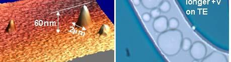
6 Forming Process ObservationofMagneliphases of intio2 Exp. setup Example of forming in TiN/HfOx/TiOx/TiN X ray diffraction TEM image Forming is thermally assisted and two step process (similar to TCM) lower forming voltage for less resistive films Creates a non stochiometric filament Possibly with morphological changes


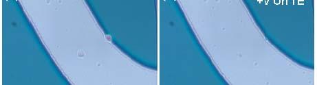
7 Oxygen Bubbles with Forming Process Forming to ON and OFF state with different polarity


 Many")

8 Interface Mechanism Oxygen vacancy profile modulation in disc region Vo is typically a shallow donor Barrier modulation (e.g. that of Schottky) Many indirect experiments supporting this simple model (next slides)


9 Ohmic Interface by Ti Layer Diffusion of Ti and chemical reaction with ihtio2 during annealing = TiO2 x


10 Switching Polarity Dependence on Ti Layer

11 Temperature Dependence for OFF/ON states Simplest model to explain observed behavior
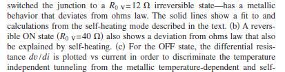
12 Thermometry Experiment
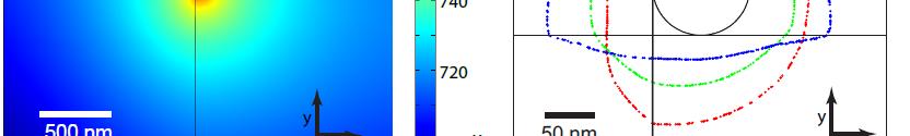
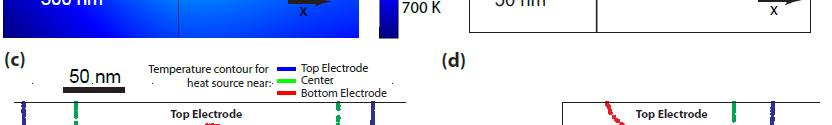
13 Chemical/Thermal/Electrical Mapping J.P. Strachan et al, Nanotechnology 211


14 Heating and Location XRF map infrared M.Janousch et al. Adv.Mat (27)
15 Bulk Mechanism
16 Vacancy Drift Model TiO x Switch Pt TiO 2 TiO 2 x Pt As fabricated, the oxide has a highly resistive TiO2 region and a conductive TiO2-x region that is highly doped with O vacancies, which are positively charged. 3 nm Pt TiO 2 TiO 2 x Pt When a positive bias voltage is applied to electrode 2, the positively charged O vacancies drift to the left, which narrows the tunneling gap. Strukov et al., Nature (28)
17 Model: Carrier Statistics E C, E D eφ(x) eφ n E G = E C E V eφ p E V, E A eφ(x) Shallow Dopants and Acceptors: n = N C F 1/2 [ (eφ n E C + eφ )/(k B T)] N C Exp[ (eφ n E C + eφ )/(k B T)] p = N VF 1/2[ (E V eφ p eφ )/(k BT)] N VExp[ (E V eφ p eφ )/(k BT)] f A = 1 1/(1+Exp[(E D eφ n eφ )/(k B T)] ]/2) 1 f D = 1 1/(1+Exp[(eφ p + eφ E A )/(k B T)] ]/2) 1
18 Defects in TiO 2 x HP s TiO 2 x C y N z devices N, C doping of TiO Calculated DOS 3 ) C concen ntration (cm C ALD 1C 15C 25C sputter Depth (normalized) Measured absorbance N co oncentration (cm -3 ) film thickness: ALD 1C 2 nm; 15C 16 nm 2C 21 nm; 25C 15 nm; sputter 6 nm sputter 25C ALD 1C 15C 2C 1 19 Depth (normalized) 1 ev TiO 2 TiO 2 x N x ev TiO 2 x TiO 2 x C y data from J.Yang Science 293, 269 (21) Science 297, 2243 (22)
19 Equilibrium Profile (v =, N D (x)/ t t = ) semiconductor with uniform N A fixed and N D (x) mobile ions 1 2 )/N D 1 N D Dopant N D (x) N A v =k BT/e E =v /L N A =8εε E G /(el) 2 Field E/E Length x/l
20 Equilibrium Profile (v =, N D (x)/ t t = ) conduction band edge )/N D semiconductor with uniform N A fixed and N D (x) mobile ions N D * /N D = 1 N D Dopant N D (x) 1 2 N A v =k BT/e E =v /L N A =8εε E G /(el) 2 Field E/E Length x/l
21 Equilibrium Profile (v =, N D (x)/ t t = ) conduction band edge Dopant N D (x) )/N D semiconductor with uniform N A fixed and N D (x) mobile ions N D * /N D = 1.1 N D N A v =k BT/e E =v /L N A =8εε E G /(el) 2 Field E/E Length x/l
22 Equilibrium Profile (v =, N D (x)/ t t = ) conduction band edge Dopant N D (x) )/N D semiconductor with uniform N A fixed and N D (x) mobile ions 1 N D * /N D = N D N A v =k BT/e E =v /L N A =8εε E G /(el) 2 Field E/E Length x/l
23 Quasi-Equilibrium Profile (v, N D D( (x)/ t t =, N D */N D =.1) v /v nt N D (x)/n DO Dopa semiconductor with uniform N A fixed and N D (x) mobile ions v/v = N D N A 1 ON state tt n + n n al φ/(e G /e) Potenti.5 v Length x/l Voltage v/v J Current J/J J =en D μ e E N A =8εε E G /(el) 2
24 Quasi-Equilibrium Profile (v, N D D( (x)/ t t =, N D */N D =.1) v /v nt N D (x)/n DO Dopa semiconductor with uniform N A fixed and N D (x) mobile ions v/v = N D N A 1 ON state tt n + n n al φ/(e G /e) Potenti.5 v J Current J/J OFF state 1 9 n + p n Length x/l Voltage v/v J =en D μ e E N A =8εε E G /(el) 2
25 Quasi-Equilibrium Profile (v, N D D( (x)/ t t =, N D */N D =.1) nt N D (x)/n DO Dopa Potenti al φ/(e G /e) semiconductor with uniform N A fixed and N D (x) mobile ions 4 4 v/v = N D N A v J Current J/J 1 ON state tt n + n n + v /v v > 1 33 v < 1 6 partial OFF state n + n p n + OFF state n + p n Length x/l Voltage v/v 1 9 J =en D μ e E N A =8εε E G /(el) 2
26 DO Dopa ant N D (x)/n D w / L 1 t / t.2 ON OFF (v = +12v ) w N A ON OFF Dynamics ial φ/(e G /e) time t/t Potenti t =L 2 /D i Cu urrent J/J Voltage v/v Voltage v/v
27 DO Dopa ant N D (x)/n D w / L 1 t / t.2 ON OFF (v = +12v ) w N A ON OFF Dynamics Potenti ial φ/(e G /e) Cu urrent J/J time t/t t =L 2 /D i Fie eld E/E 5 α Length x/l 1 w(t) = L (Av/B) 1/2 Tanh[(ABv) 1/2 t] 2 R ON w/d R OFF (1 w/d) Voltage v/v Voltage v/v
28 DO Dopa ant N D (x)/n D ON OFF (v = +12v ) OFF ON (v = 12v ) w w N A N 2 A Potenti ial φ/(e G /e) Cu urrent J/J time t/t time t/t t =L 2 /D i Voltage v/v Voltage v/v Voltage v/v Voltage v/v
29 Practical Parameters T = 3 K, v = 26 mv (v/v = 12 v = 3V) Case 1: L = 5 nm N A 8εε E G /(el) 2 = cm 3 E = 5 kv/cm E G = 3 ev N D * = cm 3 J = 4 A/cm 2 ε = 1 N D = cm 3 D Case 2: E G = 2eV.2 L= 1 nm N A cm 3 E = 25 kv/cm E G = 3 ev N D * = 1 21 cm 3 J = 2 ka/cm 2 ε = 5 N D = 1 21 cm 3 E max = 5 E, J max = 1 J (v = 3V) 5 5 nm 2 : J max =.2 μa 1 μa
30 Dynamics: Memristance 4 v/v = 12 sin[2π(t/t )/.1] Current J/J f = v t q = J t Sharp boundary Drift by ON electric field Soft boundary condition Charge q/ /q ( 1 3 ) Voltage v/v Flux f/f 1 Asymmetric Memristive


 More")

31 Bulk Resistive Switching: Experiment H.Yang et al. Nature Mat (29) More recent paper from R. Waser group (ask Brian)
32 Interfacial Switching: 1D model
 J J 1 2 1 1 1 1-1 4 12 4 B A 12 C APL")
/N DO N D 1 1 1 3 B C A Length x/l 1 APL 86, 11284")
33 Dynamics: Concentration Profile Reversal` in Bulk Device OFF ON OFF Pt BST Pt (exp) J J B A 12 C APL 73, 175 (1998) 1-2 v /v = t t Dopant D(x)/N DO N D B C A Length x/l 1 APL 86, (1998)

34 Inversion of Switching Polarity
35 Experimental Results
36 3D Model Electronic/Ionic/Thermal Model with Axial Symmetry
37 Ion drift diffusion: Fourier law: Electronic conductance: Coupled by Poisson eq: Goof paper for presentation


38
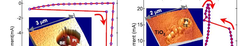
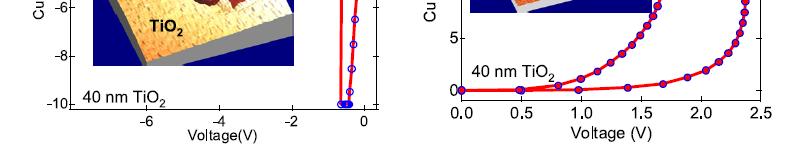
39 Scaling Prospects
40 Current Scaling V A z T = T 3 r H L H 1 X K mw rmax 5. k I k M R T = T 3 æ æ æ æ æ Vreset,V V æ æ æ æ æ æ.3 L= 3 nm H (nm) L=H I reset,ma Current is at least > 1 μa a D. Strukov, Applied Physics A, 211


")


41 Switching Time Scaling STO:Nb/STO/Ti More heating faster switching (with some saturation) Switching energy scales too Possible tradeoff with endurance and variations
42 Density Prospects Results from IMEC 212
Novel Devices and Circuits for Computing
 Novel Devices and Circuits for Computing UCSB 594BB Winter 2013 Lecture 3: ECM cell Class Outline ECM General features Forming and SET process RESET Variants and scaling prospects Equivalent model Electrochemical
Lecture 9: Metal-semiconductor junctions
 Lecture 9: Metal-semiconductor junctions Contents 1 Introduction 1 2 Metal-metal junction 1 2.1 Thermocouples.......................... 2 3 Schottky junctions 4 3.1 Forward bias............................
RRAM technology: From material physics to devices. Fabien ALIBART IEMN-CNRS, Lille
 RRAM technology: From material physics to devices Fabien ALIBART IEMN-CNRS, Lille Outline Introduction: RRAM technology and applications Few examples: Ferroelectric tunnel junction memory Mott Insulator
1. HP's memristor and applications 2. Models of resistance switching. 4. 3D circuit architectures 5. Proposal for evaluation framework
 OUTL LINE 1. HP's memristor and applications 2. Models of resistance switching 3. Volatility speed tradeo ffs 4. 3D circuit architectures 5. Proposal for evaluation framework HP S MEMRISTOR memristor =
Lecture 2. Introduction to semiconductors Structures and characteristics in semiconductors
 Lecture 2 Introduction to semiconductors Structures and characteristics in semiconductors Semiconductor p-n junction Metal Oxide Silicon structure Semiconductor contact Literature Glen F. Knoll, Radiation
Lecture 2. Introduction to semiconductors Structures and characteristics in semiconductors. Fabrication of semiconductor sensor
 Lecture 2 Introduction to semiconductors Structures and characteristics in semiconductors Semiconductor p-n junction Metal Oxide Silicon structure Semiconductor contact Fabrication of semiconductor sensor
PHYSICAL ELECTRONICS(ECE3540) CHAPTER 9 METAL SEMICONDUCTOR AND SEMICONDUCTOR HETERO-JUNCTIONS
 CHAPTER 9 METAL SEMICONDUCTOR AND SEMICONDUCTOR HETERO-JUNCTIONS") PHYSICAL ELECTRONICS(ECE3540) CHAPTER 9 METAL SEMICONDUCTOR AND SEMICONDUCTOR HETERO-JUNCTIONS Tennessee Technological University Wednesday, October 30, 013 1 Introduction Chapter 4: we considered the
PHYSICAL ELECTRONICS(ECE3540) CHAPTER 9 METAL SEMICONDUCTOR AND SEMICONDUCTOR HETERO-JUNCTIONS Tennessee Technological University Wednesday, October 30, 013 1 Introduction Chapter 4: we considered the
PHYSICAL ELECTRONICS(ECE3540) CHAPTER 9 METAL SEMICONDUCTOR AND SEMICONDUCTOR HETERO-JUNCTIONS
 CHAPTER 9 METAL SEMICONDUCTOR AND SEMICONDUCTOR HETERO-JUNCTIONS") PHYSICAL ELECTRONICS(ECE3540) CHAPTER 9 METAL SEMICONDUCTOR AND SEMICONDUCTOR HETERO-JUNCTIONS Tennessee Technological University Monday, November 11, 013 1 Introduction Chapter 4: we considered the semiconductor
PHYSICAL ELECTRONICS(ECE3540) CHAPTER 9 METAL SEMICONDUCTOR AND SEMICONDUCTOR HETERO-JUNCTIONS Tennessee Technological University Monday, November 11, 013 1 Introduction Chapter 4: we considered the semiconductor
Review Energy Bands Carrier Density & Mobility Carrier Transport Generation and Recombination
 Review Energy Bands Carrier Density & Mobility Carrier Transport Generation and Recombination The Metal-Semiconductor Junction: Review Energy band diagram of the metal and the semiconductor before (a)
Lecture 1. OUTLINE Basic Semiconductor Physics. Reading: Chapter 2.1. Semiconductors Intrinsic (undoped) silicon Doping Carrier concentrations
 silicon Doping Carrier concentrations") Lecture 1 OUTLINE Basic Semiconductor Physics Semiconductors Intrinsic (undoped) silicon Doping Carrier concentrations Reading: Chapter 2.1 EE105 Fall 2007 Lecture 1, Slide 1 What is a Semiconductor? Low
Lecture 1 OUTLINE Basic Semiconductor Physics Semiconductors Intrinsic (undoped) silicon Doping Carrier concentrations Reading: Chapter 2.1 EE105 Fall 2007 Lecture 1, Slide 1 What is a Semiconductor? Low
Supplementary Information
 Supplementary Information Ambient effects on electrical characteristics of CVD-grown monolayer MoS 2 field-effect transistors Jae-Hyuk Ahn, 1,2 William M. Parkin, 1 Carl H. Naylor, 1 A. T. Charlie Johnson,
Semiconductor Junctions
 8 Semiconductor Junctions Almost all solar cells contain junctions between different materials of different doping. Since these junctions are crucial to the operation of the solar cell, we will discuss
For the following statements, mark ( ) for true statement and (X) for wrong statement and correct it.
 for true statement and (X) for wrong statement and correct it.") Benha University Faculty of Engineering Shoubra Electrical Engineering Department First Year communications. Answer all the following questions Illustrate your answers with sketches when necessary. The
Benha University Faculty of Engineering Shoubra Electrical Engineering Department First Year communications. Answer all the following questions Illustrate your answers with sketches when necessary. The
Finding the Missing Memristor
 February 11, 29 Finding the Missing Memristor 3 nm Stan Williams HP 26 Hewlett-Packard Development Company, L.P. The information contained herein is subject to change without notice Acknowledgments People
MOS CAPACITOR AND MOSFET
 EE336 Semiconductor Devices 1 MOS CAPACITOR AND MOSFET Dr. Mohammed M. Farag Ideal MOS Capacitor Semiconductor Devices Physics and Technology Chapter 5 EE336 Semiconductor Devices 2 MOS Capacitor Structure
Lecture 15: Optoelectronic devices: Introduction
 Lecture 15: Optoelectronic devices: Introduction Contents 1 Optical absorption 1 1.1 Absorption coefficient....................... 2 2 Optical recombination 5 3 Recombination and carrier lifetime 6 3.1
Lecture 2. Introduction to semiconductors Structures and characteristics in semiconductors
 Lecture 2 Introduction to semiconductors Structures and characteristics in semiconductors Semiconductor p-n junction Metal Oxide Silicon structure Semiconductor contact Literature Glen F. Knoll, Radiation
EECS130 Integrated Circuit Devices
 EECS130 Integrated Circuit Devices Professor Ali Javey 10/02/2007 MS Junctions, Lecture 2 MOS Cap, Lecture 1 Reading: finish chapter14, start chapter16 Announcements Professor Javey will hold his OH at
Final Examination EE 130 December 16, 1997 Time allotted: 180 minutes
 Final Examination EE 130 December 16, 1997 Time allotted: 180 minutes Problem 1: Semiconductor Fundamentals [30 points] A uniformly doped silicon sample of length 100µm and cross-sectional area 100µm 2
Leakage Mechanisms. Thin films, fully depleted. Thicker films of interest for higher voltage applications. NC State
 Leakage Mechanisms Thin films, fully depleted Leakage controlled by combined thermionic / field emission across the Schottky barrier at the film-electrode interfaces. Film quality effects barrier height,
Avalanche breakdown. Impact ionization causes an avalanche of current. Occurs at low doping
 Avalanche breakdown Impact ionization causes an avalanche of current Occurs at low doping Zener tunneling Electrons tunnel from valence band to conduction band Occurs at high doping Tunneling wave decays
KATIHAL FİZİĞİ MNT-510
 KATIHAL FİZİĞİ MNT-510 YARIİLETKENLER Kaynaklar: Katıhal Fiziği, Prof. Dr. Mustafa Dikici, Seçkin Yayıncılık Katıhal Fiziği, Şakir Aydoğan, Nobel Yayıncılık, Physics for Computer Science Students: With
Symetrix Corporation Background
 Symetrix Corporation Background Symetrix has strong history as IP provider > 25 years of development >200 U.S. and foreign patents. > $70M in research revenues, royalties and other income from development.
Surfaces, Interfaces, and Layered Devices
 Surfaces, Interfaces, and Layered Devices Building blocks for nanodevices! W. Pauli: God made solids, but surfaces were the work of Devil. Surfaces and Interfaces 1 Interface between a crystal and vacuum
Schottky diodes. JFETs - MESFETs - MODFETs
 Technische Universität Graz Institute of Solid State Physics Schottky diodes JFETs - MESFETs - MODFETs Quasi Fermi level When the charge carriers are not in equilibrium the Fermi energy can be different
Section 12: Intro to Devices
 Section 12: Intro to Devices Extensive reading materials on reserve, including Robert F. Pierret, Semiconductor Device Fundamentals Bond Model of Electrons and Holes Si Si Si Si Si Si Si Si Si Silicon
Schottky Rectifiers Zheng Yang (ERF 3017,
 ECE442 Power Semiconductor Devices and Integrated Circuits Schottky Rectifiers Zheng Yang (ERF 3017, email: yangzhen@uic.edu) Power Schottky Rectifier Structure 2 Metal-Semiconductor Contact The work function
8. Schottky contacts / JFETs
 Technische Universität Graz Institute of Solid State Physics 8. Schottky contacts / JFETs Nov. 21, 2018 Technische Universität Graz Institute of Solid State Physics metal - semiconductor contacts Photoelectric
Semiconductor Physics and Devices
 The pn Junction 1) Charge carriers crossing the junction. 3) Barrier potential Semiconductor Physics and Devices Chapter 8. The pn Junction Diode 2) Formation of positive and negative ions. 4) Formation
ECE 340 Lecture 39 : MOS Capacitor II
 ECE 340 Lecture 39 : MOS Capacitor II Class Outline: Effects of Real Surfaces Threshold Voltage MOS Capacitance-Voltage Analysis Things you should know when you leave Key Questions What are the effects
Electrical and Reliability Characteristics of RRAM for Cross-point Memory Applications. Hyunsang Hwang
 Electrical and Reliability Characteristics of RRAM for Cross-point Memory Applications Hyunsang Hwang Dept. of Materials Science and Engineering Gwangju Institute of Science and Technology (GIST), KOREA
Chapter 7. The pn Junction
 Chapter 7 The pn Junction Chapter 7 PN Junction PN junction can be fabricated by implanting or diffusing donors into a P-type substrate such that a layer of semiconductor is converted into N type. Converting
Solid State Physics SEMICONDUCTORS - IV. Lecture 25. A.H. Harker. Physics and Astronomy UCL
 Solid State Physics SEMICONDUCTORS - IV Lecture 25 A.H. Harker Physics and Astronomy UCL 9.9 Carrier diffusion and recombination Suppose we have a p-type semiconductor, i.e. n h >> n e. (1) Create a local
ESE 570: Digital Integrated Circuits and VLSI Fundamentals
 ESE 570: Digital Integrated Circuits and VLSI Fundamentals Lec 4: January 23, 2018 MOS Transistor Theory, MOS Model Penn ESE 570 Spring 2018 Khanna Lecture Outline! CMOS Process Enhancements! Semiconductor
3. Two-dimensional systems
 3. Two-dimensional systems Image from IBM-Almaden 1 Introduction Type I: natural layered structures, e.g., graphite (with C nanostructures) Type II: artificial structures, heterojunctions Great technological
ESE 570: Digital Integrated Circuits and VLSI Fundamentals
 ESE 570: Digital Integrated Circuits and VLSI Fundamentals Lec 4: January 24, 2017 MOS Transistor Theory, MOS Model Penn ESE 570 Spring 2017 Khanna Lecture Outline! Semiconductor Physics " Band gaps "
Fundamentals of Semiconductor Physics
 Fall 2007 Fundamentals of Semiconductor Physics 万 歆 Zhejiang Institute of Modern Physics xinwan@zimp.zju.edu.cn http://zimp.zju.edu.cn/~xinwan/ Transistor technology evokes new physics The objective of
Semiconductor Physics fall 2012 problems
 Semiconductor Physics fall 2012 problems 1. An n-type sample of silicon has a uniform density N D = 10 16 atoms cm -3 of arsenic, and a p-type silicon sample has N A = 10 15 atoms cm -3 of boron. For each
Size-dependent Metal-insulator Transition Random Materials Crystalline & Amorphous Purely Electronic Switching
 Nanometallic RRAM I-Wei Chen Department of Materials Science and Engineering University of Pennsylvania Philadelphia, PA 19104 Nature Nano, 6, 237 (2011) Adv Mater,, 23, 3847 (2011) Adv Func Mater,, 22,
EECS130 Integrated Circuit Devices
 EECS130 Integrated Circuit Devices Professor Ali Javey 9/18/2007 P Junctions Lecture 1 Reading: Chapter 5 Announcements For THIS WEEK OLY, Prof. Javey's office hours will be held on Tuesday, Sept 18 3:30-4:30
Metal Semiconductor Contacts
 Metal Semiconductor Contacts The investigation of rectification in metal-semiconductor contacts was first described by Braun [33-35], who discovered in 1874 the asymmetric nature of electrical conduction
Consider a uniformly doped PN junction, in which one region of the semiconductor is uniformly doped with acceptor atoms and the adjacent region is
 CHAPTER 7 The PN Junction Consider a uniformly doped PN junction, in which one region of the semiconductor is uniformly doped with acceptor atoms and the adjacent region is uniformly doped with donor atoms.
Solid State Electronics. Final Examination
 The University of Toledo EECS:4400/5400/7400 Solid State Electronic Section elssf08fs.fm - 1 Solid State Electronics Final Examination Problems Points 1. 1. 14 3. 14 Total 40 Was the exam fair? yes no
Electrical Resistance
 Electrical Resistance I + V _ W Material with resistivity ρ t L Resistance R V I = L ρ Wt (Unit: ohms) where ρ is the electrical resistivity 1 Adding parts/billion to parts/thousand of dopants to pure
Current mechanisms Exam January 27, 2012
 Current mechanisms Exam January 27, 2012 There are four mechanisms that typically cause currents to flow: thermionic emission, diffusion, drift, and tunneling. Explain briefly which kind of current mechanisms
Section 12: Intro to Devices
 Section 12: Intro to Devices Extensive reading materials on reserve, including Robert F. Pierret, Semiconductor Device Fundamentals EE143 Ali Javey Bond Model of Electrons and Holes Si Si Si Si Si Si Si
Semiconductor Detectors are Ionization Chambers. Detection volume with electric field Energy deposited positive and negative charge pairs
 1 V. Semiconductor Detectors V.1. Principles Semiconductor Detectors are Ionization Chambers Detection volume with electric field Energy deposited positive and negative charge pairs Charges move in field
Introductory Nanotechnology ~ Basic Condensed Matter Physics ~
 Introductory Nanotechnology ~ Basic Condensed Matter Physics ~ Atsufumi Hirohata Department of Electronics Quick Review over the Last Lecture Classic model : Dulong-Petit empirical law c V, mol 3R 0 E
Organic Electronic Devices
 Organic Electronic Devices Week 4: Organic Photovoltaic Devices Lecture 4.1: Overview of Organic Photovoltaic Devices Bryan W. Boudouris Chemical Engineering Purdue University 1 Lecture Overview and Learning
Introduction to Optoelectronic Device Simulation by Joachim Piprek
 NUSOD 5 Tutorial MA Introduction to Optoelectronic Device Simulation by Joachim Piprek Outline:. Introduction: VCSEL Example. Electron Energy Bands 3. Drift-Diffusion Model 4. Thermal Model 5. Gain/Absorption
AN ABSTRACT OF THE THESIS OF
 AN ABSTRACT OF THE THESIS OF Santosh Murali for the degree of Master of Science in Electrical and Computer Engineering presented on December 20, 2011. Title: Investigation of Bipolar Resistive Switching
ECE 142: Electronic Circuits Lecture 3: Semiconductors
 Faculty of Engineering ECE 142: Electronic Circuits Lecture 3: Semiconductors Agenda Intrinsic Semiconductors Extrinsic Semiconductors N-type P-type Carrier Transport Drift Diffusion Semiconductors A semiconductor
Lecture 6 PN Junction and MOS Electrostatics(III) Metal-Oxide-Semiconductor Structure
 Metal-Oxide-Semiconductor Structure") Lecture 6 PN Junction and MOS Electrostatics(III) Metal-Oxide-Semiconductor Structure Outline 1. Introduction to MOS structure 2. Electrostatics of MOS in thermal equilibrium 3. Electrostatics of MOS with
Lecture 6 PN Junction and MOS Electrostatics(III) Metal-Oxide-Semiconductor Structure Outline 1. Introduction to MOS structure 2. Electrostatics of MOS in thermal equilibrium 3. Electrostatics of MOS with
UNIVERSITY OF CALIFORNIA College of Engineering Department of Electrical Engineering and Computer Sciences. EECS 130 Professor Ali Javey Fall 2006
 UNIVERSITY OF CALIFORNIA College of Engineering Department of Electrical Engineering and Computer Sciences EECS 130 Professor Ali Javey Fall 2006 Midterm 2 Name: SID: Closed book. Two sheets of notes are
junctions produce nonlinear current voltage characteristics which can be exploited
 Chapter 6 P-N DODES Junctions between n-and p-type semiconductors are extremely important foravariety of devices. Diodes based on p-n junctions produce nonlinear current voltage characteristics which can
The discussion about p-n junctions in the semiconductor device is fundamental both
 CHAPTER II MATERIALS JUNCTIONS 2.1 p-n Junctions 2.1.1 Homojunction The discussion about p-n junctions in the semiconductor device is fundamental both in modern electronic applications and in understanding
Semiconductor Physics
 Semiconductor Physics Motivation Is it possible that there might be current flowing in a conductor (or a semiconductor) even when there is no potential difference supplied across its ends? Look at the
The German University in Cairo. Faculty of Information Engineering & Technology Semiconductors (Elct 503) Electronics Department Fall 2014
 Electronics Department Fall 2014") The German University in Cairo th Electronics 5 Semester Faculty of Information Engineering & Technology Semiconductors (Elct 503) Electronics Department Fall 2014 Problem Set 3 1- a) Find the resistivity
The German University in Cairo th Electronics 5 Semester Faculty of Information Engineering & Technology Semiconductors (Elct 503) Electronics Department Fall 2014 Problem Set 3 1- a) Find the resistivity
Midterm I - Solutions
 UNIVERSITY OF CALIFORNIA College of Engineering Department of Electrical Engineering and Computer Sciences EECS 130 Spring 2008 Professor Chenming Hu Midterm I - Solutions Name: SID: Grad/Undergrad: Closed
Theory of Electrical Characterization of Semiconductors
 Theory of Electrical Characterization of Semiconductors P. Stallinga Universidade do Algarve U.C.E.H. A.D.E.E.C. OptoElectronics SELOA Summer School May 2000, Bologna (It) Overview Devices: bulk Schottky
Atmospheric pressure Plasma Enhanced CVD for large area deposition of TiO 2-x electron transport layers for PV. Heather M. Yates
 Atmospheric pressure Plasma Enhanced CVD for large area deposition of TiO 2-x electron transport layers for PV Heather M. Yates Why the interest? Perovskite solar cells have shown considerable promise
1 Name: Student number: DEPARTMENT OF PHYSICS AND PHYSICAL OCEANOGRAPHY MEMORIAL UNIVERSITY OF NEWFOUNDLAND. Fall :00-11:00
 1 Name: DEPARTMENT OF PHYSICS AND PHYSICAL OCEANOGRAPHY MEMORIAL UNIVERSITY OF NEWFOUNDLAND Final Exam Physics 3000 December 11, 2012 Fall 2012 9:00-11:00 INSTRUCTIONS: 1. Answer all seven (7) questions.
collisions of electrons. In semiconductor, in certain temperature ranges the conductivity increases rapidly by increasing temperature
 1.9. Temperature Dependence of Semiconductor Conductivity Such dependence is one most important in semiconductor. In metals, Conductivity decreases by increasing temperature due to greater frequency of
p-n junction biasing, p-n I-V characteristics, p-n currents Norlaili Mohd. Noh EEE /09
 CLASS 6&7 p-n junction biasing, p-n I-V characteristics, p-n currents 1 p-n junction biasing Unbiased p-n junction: the potential barrier is 0.7 V for Si and 0.3 V for Ge. Nett current across the p-n junction
ESE 372 / Spring 2013 / Lecture 5 Metal Oxide Semiconductor Field Effect Transistor
 Metal Oxide Semiconductor Field Effect Transistor V G V G 1 Metal Oxide Semiconductor Field Effect Transistor We will need to understand how this current flows through Si What is electric current? 2 Back
A. OTHER JUNCTIONS B. SEMICONDUCTOR HETEROJUNCTIONS -- MOLECULES AT INTERFACES: ORGANIC PHOTOVOLTAIC BULK HETEROJUNCTION DYE-SENSITIZED SOLAR CELL
 A. OTHER JUNCTIONS B. SEMICONDUCTOR HETEROJUNCTIONS -- MOLECULES AT INTERFACES: ORGANIC PHOTOVOLTAIC BULK HETEROJUNCTION DYE-SENSITIZED SOLAR CELL March 24, 2015 The University of Toledo, Department of
GaN based transistors
 GaN based transistors S FP FP dielectric G SiO 2 Al x Ga 1-x N barrier i-gan Buffer i-sic D Transistors "The Transistor was probably the most important invention of the 20th Century The American Institute
Figure 3.1 (p. 141) Figure 3.2 (p. 142)
 Figure 3.2 (p. 142)") Figure 3.1 (p. 141) Allowed electronic-energy-state systems for two isolated materials. States marked with an X are filled; those unmarked are empty. System 1 is a qualitative representation of a metal;
Figure 3.1 (p. 141) Allowed electronic-energy-state systems for two isolated materials. States marked with an X are filled; those unmarked are empty. System 1 is a qualitative representation of a metal;
MSE 310/ECE 340: Electrical Properties of Materials Fall 2014 Department of Materials Science and Engineering Boise State University
 MSE 310/ECE 340: Electrical Properties of Materials Fall 2014 Department of Materials Science and Engineering Boise State University Practice Final Exam 1 Read the questions carefully Label all figures
Characteristics and parameter extraction for NiGe/n-type Ge Schottky diode with variable annealing temperatures
 034 Chin. Phys. B Vol. 19, No. 5 2010) 057303 Characteristics and parameter extraction for NiGe/n-type Ge Schottky diode with variable annealing temperatures Liu Hong-Xia ), Wu Xiao-Feng ), Hu Shi-Gang
Challenges and Opportunities. Prof. J. Raynien Kwo 年
 Nanoelectronics Beyond Si: Challenges and Opportunities Prof. J. Raynien Kwo 年 立 Si CMOS Device Scaling Beyond 22 nm node High κ,, Metal gates, and High mobility channel 1947 First Transistor 1960 1960
Semiconductor Detectors
 Semiconductor Detectors Summary of Last Lecture Band structure in Solids: Conduction band Conduction band thermal conductivity: E g > 5 ev Valence band Insulator Charge carrier in conductor: e - Charge
Semiconductor Devices and Circuits Fall Midterm Exam. Instructor: Dr. Dietmar Knipp, Professor of Electrical Engineering. Name: Mat. -Nr.
 Semiconductor Devices and Circuits Fall 2003 Midterm Exam Instructor: Dr. Dietmar Knipp, Professor of Electrical Engineering Name: Mat. -Nr.: Guidelines: Duration of the Midterm: 1 hour The exam is a closed
Quiz #1 Practice Problem Set
 Name: Student Number: ELEC 3908 Physical Electronics Quiz #1 Practice Problem Set? Minutes January 22, 2016 - No aids except a non-programmable calculator - All questions must be answered - All questions
Hussein Ayedh. PhD Studet Department of Physics
 Hussein Ayedh PhD Studet Department of Physics OUTLINE Introduction Semiconductors Basics DLTS Theory DLTS Requirements Example Summary Introduction Energetically "deep trapping levels in semiconductor
! CMOS Process Enhancements. ! Semiconductor Physics. " Band gaps. " Field Effects. ! MOS Physics. " Cut-off. " Depletion.
 ESE 570: Digital Integrated Circuits and VLSI Fundamentals Lec 4: January 3, 018 MOS Transistor Theory, MOS Model Lecture Outline! CMOS Process Enhancements! Semiconductor Physics " Band gaps " Field Effects!
ECE 340 Lecture 27 : Junction Capacitance Class Outline:
 ECE 340 Lecture 27 : Junction Capacitance Class Outline: Breakdown Review Junction Capacitance Things you should know when you leave M.J. Gilbert ECE 340 Lecture 27 10/24/11 Key Questions What types of
Numerical Example: Carrier Concentrations
 2 Numerical ample: Carrier Concentrations Donor concentration: N d = 10 15 cm -3 Thermal equilibrium electron concentration: n o N d = 10 15 cm 3 Thermal equilibrium hole concentration: 2 2 p o = n i no
Electrical Conduction in Ceramic Materials 1 Ref: Barsoum, Fundamentals of Ceramics, Ch7, McGraw-Hill, 2000
 MME 467 Ceramics for Advanced Applications Lecture 19 Electrical Conduction in Ceramic Materials 1 Ref: Barsoum, Fundamentals of Ceramics, Ch7, McGraw-Hill, 2000 Prof. A. K. M. B. Rashid Department of
Lecture Outline. ESE 570: Digital Integrated Circuits and VLSI Fundamentals. Review: MOSFET N-Type, P-Type. Semiconductor Physics.
 ESE 57: Digital Integrated Circuits and VLSI Fundamentals Lec 4: January 24, 217 MOS Transistor Theory, MOS Model Lecture Outline! Semiconductor Physics " Band gaps " Field Effects! MOS Physics " Cutoff
Lecture 7: Extrinsic semiconductors - Fermi level
 Lecture 7: Extrinsic semiconductors - Fermi level Contents 1 Dopant materials 1 2 E F in extrinsic semiconductors 5 3 Temperature dependence of carrier concentration 6 3.1 Low temperature regime (T < T
SEMICONDUCTORS. Conductivity lies between conductors and insulators. The flow of charge in a metal results from the
 SEMICONDUCTORS Conductivity lies between conductors and insulators The flow of charge in a metal results from the movement of electrons Electros are negatively charged particles (q=1.60x10⁻¹⁹ C ) The outermost
ESE 570: Digital Integrated Circuits and VLSI Fundamentals
 ESE 570: Digital Integrated Circuits and VLSI Fundamentals Lec 4: January 29, 2019 MOS Transistor Theory, MOS Model Penn ESE 570 Spring 2019 Khanna Lecture Outline! CMOS Process Enhancements! Semiconductor
Semiconductor Device Physics
 1 Semiconductor Device Physics Lecture 3 http://zitompul.wordpress.com 2 0 1 3 Semiconductor Device Physics 2 Three primary types of carrier action occur inside a semiconductor: Drift: charged particle
Extensive reading materials on reserve, including
 Section 12: Intro to Devices Extensive reading materials on reserve, including Robert F. Pierret, Semiconductor Device Fundamentals EE143 Ali Javey Bond Model of Electrons and Holes Si Si Si Si Si Si Si
Uniform excitation: applied field and optical generation. Non-uniform doping/excitation: diffusion, continuity
 6.012 - Electronic Devices and Circuits Lecture 2 - Uniform Excitation; Non-uniform conditions Announcements Review Carrier concentrations in TE given the doping level What happens above and below room
Semiconductor Physics Problems 2015
 Semiconductor Physics Problems 2015 Page and figure numbers refer to Semiconductor Devices Physics and Technology, 3rd edition, by SM Sze and M-K Lee 1. The purest semiconductor crystals it is possible
ET3034TUx Utilization of band gap energy
 ET3034TUx - 3.3.1 - Utilization of band gap energy In the last two weeks we have discussed the working principle of a solar cell and the external parameters that define the performance of a solar cell.
Semiconductor Devices
 Semiconductor Devices - 2014 Lecture Course Part of SS Module PY4P03 Dr. P. Stamenov School of Physics and CRANN, Trinity College, Dublin 2, Ireland Hilary Term, TCD 17 th of Jan 14 Metal-Semiconductor
Chalcogenide semiconductor research and applications. Tutorial 2: Thin film characterization. Rafael Jaramillo Massachusetts Institute of Technology
 Chalcogenide semiconductor research and applications Tutorial 2: Thin film characterization Rafael Jaramillo Massachusetts Institute of Technology Section 1: Measuring composition August 20, 2017 Jaramillo
A constant potential of 0.4 V was maintained between electrodes 5 and 6 (the electrode
 (a) (b) Supplementary Figure 1 The effect of changing po 2 on the field-enhanced conductance A constant potential of 0.4 V was maintained between electrodes 5 and 6 (the electrode configuration is shown
J. Price, 1,2 Y. Q. An, 1 M. C. Downer 1 1 The university of Texas at Austin, Department of Physics, Austin, TX
 Understanding process-dependent oxygen vacancies in thin HfO 2 /SiO 2 stacked-films on Si (100) via competing electron-hole injection dynamic contributions to second harmonic generation. J. Price, 1,2
Holes (10x larger). Diode currents proportional to minority carrier densities on each side of the depletion region: J n n p0 = n i 2
. Diode currents proportional to minority carrier densities on each side of the depletion region: J n n p0 = n i 2") Part V. (40 pts.) A diode is composed of an abrupt PN junction with N D = 10 16 /cm 3 and N A =10 17 /cm 3. The diode is very long so you can assume the ends are at x =positive and negative infinity. 1.
Part V. (40 pts.) A diode is composed of an abrupt PN junction with N D = 10 16 /cm 3 and N A =10 17 /cm 3. The diode is very long so you can assume the ends are at x =positive and negative infinity. 1.
Basic Physics of Semiconductors
 Basic Physics of Semiconductors Semiconductor materials and their properties PN-junction diodes Reverse Breakdown EEM 205 Electronics I Dicle University, EEE Dr. Mehmet Siraç ÖZERDEM Semiconductor Physics
Available online at Energy Procedia 00 (2009) Energy Procedia 2 (2010) E-MRS Spring meeting 2009, Symposium B
 Energy Procedia 2 (2010) E-MRS Spring meeting 2009, Symposium B") Available online at www.sciencedirect.com Energy Procedia 00 (2009) 000 000 Energy Procedia 2 (2010) 169 176 Energy Procedia www.elsevier.com/locate/procedia www.elsevier.com/locate/procedia E-MRS Spring
Available online at www.sciencedirect.com Energy Procedia 00 (2009) 000 000 Energy Procedia 2 (2010) 169 176 Energy Procedia www.elsevier.com/locate/procedia www.elsevier.com/locate/procedia E-MRS Spring
ECE-305: Fall 2016 Minority Carrier Diffusion Equation (MCDE)
") ECE-305: Fall 2016 Minority Carrier Diffusion Equation (MCDE) Professor Peter Bermel Electrical and Computer Engineering Purdue University, West Lafayette, IN USA pbermel@purdue.edu Pierret, Semiconductor
ECE-305: Fall 2016 Minority Carrier Diffusion Equation (MCDE) Professor Peter Bermel Electrical and Computer Engineering Purdue University, West Lafayette, IN USA pbermel@purdue.edu Pierret, Semiconductor
Modeling of dielectric reliability in copper damascene interconnect systems under BTS conditions
 Modeling of dielectric reliability in copper damascene interconnect systems under BTS conditions P. Bělský 1, R. Streiter 2, H. Wolf 2, S. E. Schulz 1,2, O. Aubel 3, and T. Gessner 1,2 1 Chemnitz University
Lecture 5 Junction characterisation
 Lecture 5 Junction characterisation Jon Major October 2018 The PV research cycle Make cells Measure cells Despair Repeat 40 1.1% 4.9% Data Current density (ma/cm 2 ) 20 0-20 -1.0-0.5 0.0 0.5 1.0 Voltage
The photovoltaic effect occurs in semiconductors where there are distinct valence and
 How a Photovoltaic Cell Works The photovoltaic effect occurs in semiconductors where there are distinct valence and conduction bands. (There are energies at which electrons can not exist within the solid)
Metallic: 2n 1. +n 2. =3q Armchair structure always metallic = 2
 Properties of CNT d = 2.46 n 2 2 1 + n1n2 + n2 2π Metallic: 2n 1 +n 2 =3q Armchair structure always metallic a) Graphite Valence(π) and Conduction(π*) states touch at six points(fermi points) Carbon Nanotube: