Digital Microelectronic Circuits ( )
|
|
|
- Marcus Preston
- 5 years ago
- Views:
Transcription

1 Digital Microelectronic ircuits ( ) Presented by: Dr. Alex Fish Lecture 5: Parasitic apacitance and Driving a Load 1
2 Motivation Thus far, we have learned how to model our essential building block, the MOSFET transistor, and how to use these building blocks to create the most popular logic family, Static MOS. We analyzed the characteristics of a static MOS inverter, including its Static and Dynamic Properties. We saw that both the delay and the power consumption of a MOS gate depend on the load capacitance of the gate. t 0.69R P f V 2 pd eq Load dynamic DD 2
3 What will we learn today? Today, we will go back to our MOSFET transistor to try and understand what parasitic capacitances are inherent to its structure. Then, we will develop a model for equivalent capacitance estimation for delay calculation of a MOS inverter. Accordingly, we will examine the optimal sizing of a MOS gate. And finally, we will develop a methodology for sizing a chain of inverters to drive a large load. 3
4 What will we learn today? 5.1 MOSFET apacitance 5.2 Inverter Delay apacitance Model 5.3 Driving a Load 4


5 MOSFET apacitance 5.2 Inverter Delay apacitance Model 5.3 Driving a Load So back to our device, let s see what parasitic capacitances we have: MOSFET APAITANE 5
6 MOSFET apacitance One of the important parameters of a MOS Transistor is its capacitance. The MOSFET has two major categories of capacitance:» Gate/hannel apacitance capacitance caused by the insulating oxide layer under the gate.» Junction apacitance pn-junction capacitance between the diffusions and the substrate. t ox GS GD n + L n + G SB p-substrate DB 6
7 Gate apacitance The Gate apacitance includes:» Gate to hannel apacitance, G : The main capacitance that is dependent on the region of operation. In general: ox G WL oxwl tox» Gate Overlap apacitance, GDO, GSO : A constant (small) capacitance caused by gate overlap of the diffusions. W GSO GDO Overlap 7
8 Gate apacitance Looking at gate capacitance as a function of biasing shows how it changes.» In accumulation, the capacitance is across the oxide.» As V GS grows, the depletion layer decreases the capacitance (as if the dielectric gets longer)» Once the channel is formed, the capacitance jumps.» At pinch-off, the drain capacitance drops to zero. 8
9 Gate apacitance 9

10 Gate apacitance To model this non-linear behavior, we will use the following approximations: All capacitance is towards substrate GB WL ox apacitance symmetrically divided between source and drain GS GD WL ox 2 All capacitance to Source Question: How do we relate to Velocity Saturation? GS 2 3 WL ox 10

11 Junction (Diffusion) apacitance The Junction apacitance is the diffusion capacitance of the MOSFET. This is measured according to fabrication parameters diff bottom side walls Area Perimiter j jsw L W 2L W j diff jsw diff Diffusion cap is non-linear and voltage dependent. For simplicity, we will take it as constant in this course. 11
12 MOSFET apacitance Summary Dependence of MOS capacitances on W and L: 12

13 MOSFET apacitance Summary G GS GD GS GS GSO S D GD GD GDO GB GB SB GB DB SB Sdiff DB Ddiff B 13


14 MOSFET apacitance 5.2 Inverter Delay apacitance Model 5.3 Driving a Load OK, so we saw that the MOSFET has a bunch of non-linear parasitic capacitances, which makes them tough to use. To simplify life we ll now develop an: INVERTER DELAY APAITANE MODEL 14
15 apacitance Modeling As we saw, MOSFET capacitances are non-constant and non-linear. Therefore, it is hard to solve a general equation for an arbitrary transition/operation. Instead, we will develop a simple model that will approximate the capacitances during a specific transition that interests us. In this case, we are looking for the Load apacitance to use when finding the gate delay. Therefore, we will apply a step function to the input of an inverter and approximate the capacitances according to the MOSFET parasitics we just learned. 15
16 apacitance Modeling Let s look at a MOS inverter with all its parasitic capacitances:» onsidering the Gates of the transistors are the inputs to the inverter, any capacitor touching the gate should be considered input capacitance. V in» onsidering the Drains of the transistors are connected to the inverter output, any capacitor touching the Drains should be considered output capacitance. G GDP GSP GDN G GSN B GBN S GBP D D B S SBP DBP V out DBN SBN 16
17 apacitance Modeling We have to differentiate between output (intrinsic) capacitances and load (extrinsic) capacitances. Driver Load wire out,1 in,2 int ext Our total load capacitance is Load out,1 wire in,2 17


18 Intrinsic (Output) apacitance We ll now look at what makes up the intrinsic output capacitance of the driver. This is primarily made up of diffusion capacitances:» Both drain-to-body capacitances have a terminal with a constant voltage and the other connected to the output.» For a simple computation, we will replace them with an equivalent capacitance to ground.» These capacitances are very non-linear and we will not go into their calculation in this course. DBP DBP + DBN DBN 18
19 Intrinsic (Output) apacitance How about feedthrough capacitance?» Taking the input step as ideal, the gate-to-source and gate-to-body capacitances don t contribute to the propagation delay.» The source-to-body capacitance is shorted to the supply, so it doesn t switch. GSP + GBP GDP + GDN What about the gate-to-drain capacitance?» While the gate voltage rises (V in ), the drain voltage drops (V out ) and vice versa.» According to the Miller Effect, we can move this capacitance relative to ground, doubling its value.» This can be regarded as overlap capacitance, as for the majority of the transition the devices are in cutoff or saturation. GSN + GBN 2( GDP + GDN ) 19
20 The Miller Effect A capacitor experiencing identical, but opposite voltage swings at both its terminals can be replaced by a capacitor to ground, whose value is twice the original value. 20
21 Summary of Intrinsic Output ap 21
22 External apacitance Now, to annotate the parasitics during switching, we will cascade another inverter after the first. We first add the Wire apacitance. Then we add the gate capacitances of the second inverter.» These are approximately the oxide capacitance times the area: W L W L GN 2 GP2 OX N 2 N 2 P2 P2» Again, we can just add the pmos gate capacitance to the general capacitance to ground. P1 N1 W GP2 GN2 P2 N2 22
23 External apacitance What happened to overlap capacitance and the Miller Effect on GD2?» Remember that this is an approximate model, but» L=L eff +2*L ov, so G = ox *W*L drawn.» During the transient, for most of the time the load gate s transistors are in cutoff or in linear.» Miller effect won t appear, because the second gate won t switch until t pd1 is over. Therefore:» YES, GD2 and GS2 contribute to the load capacitance.» BUT, a good approximation is just G2 = OX *W*L 23
24 Summary of Next Stage Input ap 24
25 Parasitic apacitances - Summary Altogether, as a very general approximation, we get: 2( ) load GDP1 GDN 1 DBP1 DBN 1 GP2 GN 2 W Miller Diffusion Load GP2 An even more general approximation with N fan-out gates gives us: load out wire N in GDP1 + GDN1 P1 DBP1 P2 N1 DBN1 + W N2 GN2 25
26 Last Time MOS Inverter apacitance Model for t pd. 26
: Gate cap, no miller N load out wire in")
27 Last Time MOS apacitance Model» Driver ap ( out or int ): Diffusion + Miller» Load ap ( in or g ): Gate cap, no miller N load out wire in 27


28 MOSFET apacitance 5.2 Inverter Delay apacitance Model 5.3 Driving a Load Up till now, we discussed device sizing with an optimal fanout of 1. What happens if we want to cascade more gates to the output? DRIVING A LOAD 28
29 External apacitance Up till now, we assumed our inverter was only driving a copy of itself. This is known as intrinsic or unloaded delay. But we usually will have a larger fanout, and in some cases, we will need to drive large loads. Let s remember how we defined our load capacitance: load diff overlap fanout wire int ext We can now write our delay equation according to these components. t 0.69R 0.69R pd eq load eq int ext Driver out,1 int ext Load wire in,2 29
30 Sizing Factor (S) t 0.69R pd eq int ext This means that if we add a larger load, our delay will increase. This is intuitive, as it means we have to supply more current from the same source. If we were to widen our transistors by a factor S, this would decrease our resistance and increase our intrinsic * * capacitance. S R R S int int eq eq 30
31 S R R S * * int int eq eq Sizing Factor (S) t 0.69R pd eq int ext These two factors trade-off, which is why we get an optimal inverter size. * * * Req tpd unloaded 0.69Req 0.69 S 0.69Req S, int int int However, upsizing our gate doesn t affect the external capacitance and therefore decreases the loaded delay. R * eq ext ext t pd 0.69 Sint ext 0.69Req int 1 t p0 1 S Sint Sint 31

32 Sizing Factor (S) t t p t p R ext p0 eq int S int 32
33 Driving a Large Load So now we have a very large load to drive. We could just use a very large inverter.» But then someone would have to drive this large inverter. So considering we start with a limited input capacitance, how should we best drive this load? 34
34 Inverter hain In Out L If L is given:» How many stages are needed to minimize the delay?» How to size the inverters? Anyone want to guess the solution? 35
35 Delay Optimization Problem #1 To solve an optimization problem, we need a set of constraints:» Load apacitance.» Number of Inverters.» Size of input capacitance. 36
36 Delay Optimization Problem #1 To explore this problem, we must define a proportionality factor, γ. γ is a function of technology*, that describes the relationship between a gate s input gate capacitance ( g ) and its intrinsic output capacitance ( int ): int * γ is close to 1 for most submicron processes! g 37

37 Delay Optimization Problem #1 Now, we will write the delay as a function of γ, and the effective fanout, f: ext f t pd t p0 1 t p01 f g int ext g g We can see that the delay for a certain technology is only a function of the effective fanout! 38

38 Inverter with Load So we see that the delay increases with ratio of load to inverter size: t t p p0 1 f t p0 is the intrinsic delay of an unloaded inverter. γ is a technology dependent ratio. f is the Effective Fanout ratio of load to inverter size 39
39 Sizing a chain of inverters Now we will express the delay of a chain of inverters: t t p p0 1 f Assuming a negligible wire capacitance, for the j-th stage, we get: f t t t j g, j1 pd, j p0 1 p0 1 g, j And we can write the total delay as: N N g, j1 pd pd, j p0 1 j1 j1 g, j t t t 40
40 Sizing a chain of inverters We have N-1 unknowns, so we will derive N-1 partial derivatives: t g, j We receive a set of constraints: pd 0 t pd t p0 N 1 g, j1 j 1 g, j g, j1 g, j g, j g, j1 This means that: g, j g, j 1 g, j 1» Each inverter is sized up by the same factor, f.» Each inverter has the same effective fanout, f j =f.» Each inverter has the same delay, t p0 (1+f/ γ). 41
41 Sizing a chain of inverters Now this is interesting what if we multiply the fanout of each stage?: f N N N g, j1 g,2 g,3 g,4 g, N load load f j j1 j1 g, j g,1 g,2 g,3 g, N 1 g, N g,1 We found the ratio between input and load capacitance! f N / F load g,1 N F load g,1 42
42 Sizing a chain of inverters f N F g,1 We defined the overall effective fanout, F, between the input and load capacitance of the circuit. Using this parameter, we can express the total delay: t pd N t p0 1 N F F load 43
43 Example: 3 Stages In S=1 S=2 S=4 Out 1 1 f f 2 L = 8 1 L / 1 has to be evenly distributed across N = 3 stages: f
44 Delay Optimization Problem #2 Great but what is the optimal Number of Stages? This is a new Optimization Problem. You are given:» The size of the first inverter» The size of the load that needs to be driven Your goal:» Minimize delay by finding optimal number and sizes of gates So, need to find N that minimizes: t p N t p0 1 N F 45
45 Delay Optimization Problem #2 Starting with a minimum sized inverter with g,min, and driving a given load, load, we can see that:» With a small number of stages, we get a large delay due to the effective fanout (f, F).» With a large number of stages, we get a large delay due to the intrinsic delay (Nt p0 ) t pd N t p0 1 N F To find the optimal number of stages, we will differentiate and equate to zero. dt pd dn 0 N N F ln F F 0 fopt exp1 N f opt 46
46 Delay Optimization Problem #2 This equation only has an analytical solution for the case of γ=0. In this esoteric case we get: f opt exp 1 f opt fopt e Nopt 0 ln F If we take the typical case of γ=1, we can numerically solve the equation and arrive at: f opt 3.6 N log opt F 47
47 We are given: We need to find the optimal number of stages, so f opt =4. F N opt L in 64 L in 4 64 Example min log F log 64 3 f opt min So we need 3 stages that will be sized 1, 4, 16. Let s inspect what delay we would have gotten with various number of stages. 48
48 Example t pd N t p0 1 N F N f t p
49 Normalized delay function of F Let s consider the trade offs of driving loads with various approaches:» Unbuffered» Two-Stages» Optimal FO4 hain t pd N t p0 1 N F For a small load, F=10:» Unbuffered delay: t pd =11t p0» Two Stage delay: t pd =8.3t p0» Optimal FO4 hain: N opt =2t pd =8.3t p0 50
50 Normalized delay function of F For a slightly larger load, F=100:» Unbuffered delay: t pd =101t p0» Two Stage delay: t pd =22t p0» Optimal FO4 hain: N opt =4 t pd =16.6t p0» We see a large benefit for one extra stage, but the inverter chain might not be worth it. How about a really large load, F=10000:» Unbuffered delay: t pd =10001t p0» Two Stage delay: t pd =202t p0 t pd N t p0 1 N F» Optimal FO4 hain: N opt =7 t pd =33.1t p0» But we pay for this with a large number of stages and huge final stage inverter (W=1mm) 51
51 What about Energy (and Area)? How much additional Energy (and Area) does an inverter chain cost?» Using a single (minimal) inverter, our capacitance would be: 1 stage min min L» But the capacitance of N stages 1 1 f... 1 f N 1 N stages min min min L 1 f... 1 f N 1 1stage min min Overhead! 52
52 What about Energy (and Area)? So the overhead cap is: 1 f 1 f... f overhead N 2 min N fmin f f For example: L 20 pf, min 50 ff 20 pf 5 F 400, Nopt 5, f ff overhead pf 4 53

53 Example Overhead Numbers For the previous example: 54
54 onclusions In order to drive a large load, we should:» Use a chain of inverters.» Each inverter should increase its size by the same amount.» To minimize the delay, we should set the effective fanout to about 4. Remember!» You have to use a whole number of stages (i.e. you can t choose 2.5 stages).» Therefore, choose the closest number of stages for close to optimal effective fanout..» hoose according to signal polarity or optimal speed.» But fewer stages means less power! 55
Practice 7: CMOS Capacitance
 Practice 7: CMOS Capacitance Digital Electronic Circuits Semester A 2012 MOSFET Capacitances MOSFET Capacitance Components 3 Gate to Channel Capacitance In general, the gate capacitance is similar to a
Check course home page periodically for announcements. Homework 2 is due TODAY by 5pm In 240 Cory
 EE141 Fall 005 Lecture 6 MOS Capacitances, Propagation elay Important! Check course home page periodically for announcements Homework is due TOAY by 5pm In 40 Cory Homework 3 will be posted TOAY ue Thursday
MOSFET: Introduction
 E&CE 437 Integrated VLSI Systems MOS Transistor 1 of 30 MOSFET: Introduction Metal oxide semiconductor field effect transistor (MOSFET) or MOS is widely used for implementing digital designs Its major
ECE321 Electronics I
 ECE31 Electronics Lecture 1: CMOS nverter: Noise Margin & Delay Model Payman Zarkesh-Ha Office: ECE Bldg. 30B Office hours: Tuesday :00-3:00PM or by appointment E-mail: payman@ece.unm.edu Slide: 1 CMOS
EE 466/586 VLSI Design. Partha Pande School of EECS Washington State University
 EE 466/586 VLSI Design Partha Pande School of EECS Washington State University pande@eecs.wsu.edu Lecture 9 Propagation delay Power and delay Tradeoffs Follow board notes Propagation Delay Switching Time
! MOS Capacitances. " Extrinsic. " Intrinsic. ! Lumped Capacitance Model. ! First Order Capacitor Summary. ! Capacitance Implications
 ESE 570: Digital Integrated Circuits and VLSI Fundamentals Lec 7: February, 07 MOS SPICE Models, MOS Parasitic Details Lecture Outline! MOS Capacitances " Extrinsic " Intrinsic! Lumped Capacitance Model!
5.0 CMOS Inverter. W.Kucewicz VLSICirciuit Design 1
 5.0 CMOS Inverter W.Kucewicz VLSICirciuit Design 1 Properties Switching Threshold Dynamic Behaviour Capacitance Propagation Delay nmos/pmos Ratio Power Consumption Contents W.Kucewicz VLSICirciuit Design
VLSI Design and Simulation
 VLSI Design and Simulation Performance Characterization Topics Performance Characterization Resistance Estimation Capacitance Estimation Inductance Estimation Performance Characterization Inverter Voltage
EE115C Winter 2017 Digital Electronic Circuits. Lecture 3: MOS RC Model, CMOS Manufacturing
 EE115C Winter 2017 Digital Electronic Circuits Lecture 3: MOS RC Model, CMOS Manufacturing Agenda MOS Transistor: RC Model (pp. 104-113) S R on D CMOS Manufacturing Process (pp. 36-46) S S C GS G G C GD
The Physical Structure (NMOS)
") The Physical Structure (NMOS) Al SiO2 Field Oxide Gate oxide S n+ Polysilicon Gate Al SiO2 SiO2 D n+ L channel P Substrate Field Oxide contact Metal (S) n+ (G) L W n+ (D) Poly 1 Transistor Resistance Two
The Physical Structure (NMOS) Al SiO2 Field Oxide Gate oxide S n+ Polysilicon Gate Al SiO2 SiO2 D n+ L channel P Substrate Field Oxide contact Metal (S) n+ (G) L W n+ (D) Poly 1 Transistor Resistance Two
The CMOS Inverter: A First Glance
 The CMOS Inverter: A First Glance V DD S D V in V out C L D S CMOS Inverter N Well V DD V DD PMOS 2λ PMOS Contacts In Out In Out Metal 1 NMOS Polysilicon NMOS GND CMOS Inverter: Steady State Response V
MOS Transistor Theory
 CHAPTER 3 MOS Transistor Theory Outline 2 1. Introduction 2. Ideal I-V Characteristics 3. Nonideal I-V Effects 4. C-V Characteristics 5. DC Transfer Characteristics 6. Switch-level RC Delay Models MOS
ECE321 Electronics I
 EE31 Electronics I Lecture 8: MOSET Threshold Voltage and Parasitic apacitances Payman Zarkesh-Ha Office: EE Bldg. 3B Office hours: Tuesday :-3:PM or by appointment E-mail: payman@ece.unm.edu Slide: 1
COMP 103. Lecture 10. Inverter Dynamics: The Quest for Performance. Section 5.4.2, What is this lecture+ about? PERFORMANCE
 COMP 103 Lecture 10 Inverter Dynamics: The Quest for Performance Section 5.4.2, 5.4.3 [All lecture notes are adapted from Mary Jane Irwin, Penn State, which were adapted from Rabaey s Digital Integrated
ESE 570: Digital Integrated Circuits and VLSI Fundamentals
 ESE 570: Digital Integrated Circuits and VLSI Fundamentals Lec 7: February 4, 2016 MOS SPICE Models, MOS Parasitic Details Lecture Outline! MOS Capacitances " Extrinsic " Intrinsic! Lumped Capacitance
The Inverter. Digital Integrated Circuits A Design Perspective. Jan M. Rabaey Anantha Chandrakasan Borivoje Nikolic
 Digital Integrated Circuits A Design Perspective Jan M. Rabaey Anantha Chandrakasan Borivoje Nikolic The Inverter Revised from Digital Integrated Circuits, Jan M. Rabaey el, 2003 Propagation Delay CMOS
Digital Microelectronic Circuits ( ) The CMOS Inverter. Lecture 4: Presented by: Adam Teman
 The CMOS Inverter. Lecture 4: Presented by: Adam Teman") Digital Microelectronic Circuits (361-1-301 ) Presented by: Adam Teman Lecture 4: The CMOS Inverter 1 Last Lectures Moore s Law Terminology» Static Properties» Dynamic Properties» Power The MOSFET Transistor»
Digital Microelectronic Circuits (361-1-301 ) Presented by: Adam Teman Lecture 4: The CMOS Inverter 1 Last Lectures Moore s Law Terminology» Static Properties» Dynamic Properties» Power The MOSFET Transistor»
Announcements. EE141- Fall 2002 Lecture 7. MOS Capacitances Inverter Delay Power
 - Fall 2002 Lecture 7 MOS Capacitances Inverter Delay Power Announcements Wednesday 12-3pm lab cancelled Lab 4 this week Homework 2 due today at 5pm Homework 3 posted tonight Today s lecture MOS capacitances
THE INVERTER. Inverter
 THE INVERTER DIGITAL GATES Fundamental Parameters Functionality Reliability, Robustness Area Performance» Speed (delay)» Power Consumption» Energy Noise in Digital Integrated Circuits v(t) V DD i(t) (a)
Lecture 4: CMOS Transistor Theory
 Introduction to CMOS VLSI Design Lecture 4: CMOS Transistor Theory David Harris, Harvey Mudd College Kartik Mohanram and Steven Levitan University of Pittsburgh Outline q Introduction q MOS Capacitor q
EEC 116 Lecture #3: CMOS Inverters MOS Scaling. Rajeevan Amirtharajah University of California, Davis Jeff Parkhurst Intel Corporation
 EEC 116 Lecture #3: CMOS Inverters MOS Scaling Rajeevan Amirtharajah University of California, Davis Jeff Parhurst Intel Corporation Outline Review: Inverter Transfer Characteristics Lecture 3: Noise Margins,
EE105 Fall 2014 Microelectronic Devices and Circuits. NMOS Transistor Capacitances: Saturation Region
 EE105 Fall 014 Microelectronic Devices and Circuits Prof. Ming C. Wu wu@eecs.berkeley.edu 511 Sutardja Dai Hall (SDH) 1 NMOS Transistor Capacitances: Saturation Region Drain no longer connected to channel
Lecture 3: CMOS Transistor Theory
 Lecture 3: CMOS Transistor Theory Outline Introduction MOS Capacitor nmos I-V Characteristics pmos I-V Characteristics Gate and Diffusion Capacitance 2 Introduction So far, we have treated transistors
MOS Transistor Theory
 MOS Transistor Theory So far, we have viewed a MOS transistor as an ideal switch (digital operation) Reality: less than ideal EE 261 Krish Chakrabarty 1 Introduction So far, we have treated transistors
Integrated Circuits & Systems
 Federal University of Santa Catarina Center for Technology Computer Science & Electronics Engineering Integrated Circuits & Systems INE 5442 Lecture 14 The CMOS Inverter: dynamic behavior (sizing, inverter
Chapter 4 Field-Effect Transistors
 Chapter 4 Field-Effect Transistors Microelectronic Circuit Design Richard C. Jaeger Travis N. Blalock 5/5/11 Chap 4-1 Chapter Goals Describe operation of MOSFETs. Define FET characteristics in operation
Digital Integrated Circuits
 Digital Integrated ircuits YuZhuo Fu contact:fuyuzhuo@ic.sjtu.edu.cn Office location:47 room WeiDianZi building,no 800 Donghuan road,minhang amus Introduction Digital I 3.MOS Inverter Introduction Digital
The Devices. Digital Integrated Circuits A Design Perspective. Jan M. Rabaey Anantha Chandrakasan Borivoje Nikolic. July 30, 2002
 Digital Integrated Circuits A Design Perspective Jan M. Rabaey Anantha Chandrakasan Borivoje Nikolic The Devices July 30, 2002 Goal of this chapter Present intuitive understanding of device operation Introduction
University of Pennsylvania Department of Electrical Engineering. ESE 570 Midterm Exam March 14, 2013 FORMULAS AND DATA
 University of Pennsylvania Department of Electrical Engineering ESE 570 Midterm Exam March 4, 03 FORMULAS AND DATA. PHYSICAL CONSTANTS: n i = intrinsic concentration undoped) silicon =.45 x 0 0 cm -3 @
EE141-Fall Digital Integrated Circuits. Announcements. Lab #2 Mon., Lab #3 Fri. Homework #3 due Thursday. Homework #4 due next Thursday
 EE4-Fall 2000 Digital Integrated ircuits Lecture 6 Inverter Delay Optimization Announcements Lab #2 Mon., Lab #3 Fri. Homework #3 due Thursday Homework #4 due next Thursday 2 2 lass Material Last lecture
The CMOS Inverter: A First Glance
 The CMOS Inverter: A First Glance V DD V in V out C L CMOS Properties Full rail-to-rail swing Symmetrical VTC Propagation delay function of load capacitance and resistance of transistors No static power
EEC 118 Lecture #5: CMOS Inverter AC Characteristics. Rajeevan Amirtharajah University of California, Davis Jeff Parkhurst Intel Corporation
 EEC 8 Lecture #5: CMOS Inverter AC Characteristics Rajeevan Amirtharajah University of California, Davis Jeff Parkhurst Intel Corporation Acknowledgments Slides due to Rajit Manohar from ECE 547 Advanced
ESE570 Spring University of Pennsylvania Department of Electrical and System Engineering Digital Integrated Cicruits AND VLSI Fundamentals
 University of Pennsylvania Department of Electrical and System Engineering Digital Integrated Cicruits AND VLSI Fundamentals ESE570, Spring 2018 Final Monday, Apr 0 5 Problems with point weightings shown.
VLSI Design I; A. Milenkovic 1
 Review Voltage wing of PT Driving an Inverter PE/EE 47, PE 57 VLI Design I L9: MO & Wire apacitances Department of Electrical and omputer Engineering University of labama in Huntsville leksandar Milenkovic
EE 435. Lecture 37. Parasitic Capacitances in MOS Devices. String DAC Parasitic Capacitances
 EE 435 Lecture 37 Parasitic Capacitances in MOS Devices String DAC Parasitic Capacitances Parasitic Capacitors in MOSFET (will initially consider two) Parasitic Capacitors in MOSFET C GCH Parasitic Capacitors
EEC 118 Lecture #2: MOSFET Structure and Basic Operation. Rajeevan Amirtharajah University of California, Davis Jeff Parkhurst Intel Corporation
 EEC 118 Lecture #2: MOSFET Structure and Basic Operation Rajeevan Amirtharajah University of California, Davis Jeff Parkhurst Intel Corporation Announcements Lab 1 this week, report due next week Bring
MOS Transistor I-V Characteristics and Parasitics
 ECEN454 Digital Integrated Circuit Design MOS Transistor I-V Characteristics and Parasitics ECEN 454 Facts about Transistors So far, we have treated transistors as ideal switches An ON transistor passes
CMPEN 411 VLSI Digital Circuits Spring 2012
 CMPEN 411 VLSI Digital Circuits Spring 2012 Lecture 09: Resistance & Inverter Dynamic View [Adapted from Rabaey s Digital Integrated Circuits, Second Edition, 2003 J. Rabaey, A. Chandrakasan, B. Nikolic]
Digital Microelectronic Circuits ( ) Logical Effort. Lecture 7: Presented by: Adam Teman
 Logical Effort. Lecture 7: Presented by: Adam Teman") Digital Microelectronic ircuits (361-1-3021 ) Presented by: Adam Teman Lecture 7: Logical Effort Digital Microelectronic ircuits The VLSI Systems enter - BGU Lecture 7: Logical Effort 1 Last Lectures The
Digital Microelectronic ircuits (361-1-3021 ) Presented by: Adam Teman Lecture 7: Logical Effort Digital Microelectronic ircuits The VLSI Systems enter - BGU Lecture 7: Logical Effort 1 Last Lectures The
Chapter 5. The Inverter. V1. April 10, 03 V1.1 April 25, 03 V2.1 Nov Inverter
 Chapter 5 The Inverter V1. April 10, 03 V1.1 April 25, 03 V2.1 Nov.12 03 Objective of This Chapter Use Inverter to know basic CMOS Circuits Operations Watch for performance Index such as Speed (Delay calculation)
ENEE 359a Digital VLSI Design
 SLIDE 1 ENEE 359a Digital VLSI Design & Logical Effort Prof. blj@ece.umd.edu Credit where credit is due: Slides contain original artwork ( Jacob 2004) as well as material taken liberally from Irwin & Vijay
Interconnect (2) Buffering Techniques. Logical Effort
 Buffering Techniques. Logical Effort") Interconnect (2) Buffering Techniques. Logical Effort Lecture 14 18-322 Fall 2002 Textbook: [Sections 4.2.1, 8.2.3] A few announcements! M1 is almost over: The check-off is due today (by 9:30PM) Students
Interconnect (2) Buffering Techniques. Logical Effort Lecture 14 18-322 Fall 2002 Textbook: [Sections 4.2.1, 8.2.3] A few announcements! M1 is almost over: The check-off is due today (by 9:30PM) Students
Introduction to CMOS VLSI. Chapter 2: CMOS Transistor Theory. Harris, 2004 Updated by Li Chen, Outline
 Introduction to MOS VLSI Design hapter : MOS Transistor Theory copyright@david Harris, 004 Updated by Li hen, 010 Outline Introduction MOS apacitor nmos IV haracteristics pmos IV haracteristics Gate and
ECE 438: Digital Integrated Circuits Assignment #4 Solution The Inverter
 ECE 438: Digital Integrated Circuits Assignment #4 The Inverter Text: Chapter 5, Digital Integrated Circuits 2 nd Ed, Rabaey 1) Consider the CMOS inverter circuit in Figure P1 with the following parameters.
ELEC 3908, Physical Electronics, Lecture 26. MOSFET Small Signal Modelling
 ELEC 3908, Physical Electronics, Lecture 26 MOSFET Small Signal Modelling Lecture Outline MOSFET small signal behavior will be considered in the same way as for the diode and BJT Capacitances will be considered
Lecture 5: CMOS Transistor Theory
 Lecture 5: CMOS Transistor Theory Slides courtesy of Deming Chen Slides based on the initial set from David Harris CMOS VLSI Design Outline q q q q q q q Introduction MOS Capacitor nmos I-V Characteristics
Homework #2 10/6/2016. C int = C g, where 1 t p = t p0 (1 + C ext / C g ) = t p0 (1 + f/ ) f = C ext /C g is the effective fanout
 = t p0 (1 + f/ ) f = C ext /C g is the effective fanout") 0/6/06 Homework # Lecture 8, 9: Sizing and Layout of omplex MOS Gates Reading: hapter 4, sections 4.3-4.5 October 3 & 5, 06 hapter, section.5.5 Prof. R. Iris ahar Weste & Harris vailable on course webpage
0/6/06 Homework # Lecture 8, 9: Sizing and Layout of omplex MOS Gates Reading: hapter 4, sections 4.3-4.5 October 3 & 5, 06 hapter, section.5.5 Prof. R. Iris ahar Weste & Harris vailable on course webpage
EEE 421 VLSI Circuits
 EEE 421 CMOS Properties Full rail-to-rail swing high noise margins» Logic levels not dependent upon the relative device sizes transistors can be minimum size ratioless Always a path to V dd or GND in steady
Lecture Outline. ESE 570: Digital Integrated Circuits and VLSI Fundamentals. Review: CMOS Inverter: Visual VTC. Review: CMOS Inverter: Visual VTC
 ESE 570: Digital Integrated Circuits and LSI Fundamentals Lec 0: February 4, 207 MOS Inverter: Dynamic Characteristics Lecture Outline! Review: Symmetric CMOS Inverter Design! Inverter Power! Dynamic Characteristics
Lecture 12 CMOS Delay & Transient Response
 EE 471: Transport Phenomena in Solid State Devices Spring 2018 Lecture 12 CMOS Delay & Transient Response Bryan Ackland Department of Electrical and Computer Engineering Stevens Institute of Technology
HW 5 posted due in two weeks Lab this week Midterm graded Project to be launched in week 7
 HW 5 posted due in two weeks Lab this week Midterm graded Project to be launched in week 7 2 What do digital IC designers need to know? 5 EE4 EECS4 6 3 0< V GS - V T < V DS Pinch-off 7 For (V GS V T )
! PN Junction. ! MOS Transistor Topology. ! Threshold. ! Operating Regions. " Resistive. " Saturation. " Subthreshold (next class)
") ESE370: ircuitlevel Modeling, Design, and Optimization for Digital Systems Lec 7: September 20, 2017 MOS Transistor Operating Regions Part 1 Today! PN Junction! MOS Transistor Topology! Threshold! Operating
ESE370: ircuitlevel Modeling, Design, and Optimization for Digital Systems Lec 7: September 20, 2017 MOS Transistor Operating Regions Part 1 Today! PN Junction! MOS Transistor Topology! Threshold! Operating
CMOS INVERTER. Last Lecture. Metrics for qualifying digital circuits. »Cost» Reliability» Speed (delay)»performance
»performance") CMOS INVERTER Last Lecture Metrics for qualifying digital circuits»cost» Reliability» Speed (delay)»performance 1 Today s lecture The CMOS inverter at a glance An MOS transistor model for manual analysis
CMOS INVERTER Last Lecture Metrics for qualifying digital circuits»cost» Reliability» Speed (delay)»performance 1 Today s lecture The CMOS inverter at a glance An MOS transistor model for manual analysis
Digital Integrated Circuits (83-313) Lecture 5: Interconnect. Semester B, Lecturer: Adam Teman TAs: Itamar Levi, Robert Giterman 1
 Lecture 5: Interconnect. Semester B, Lecturer: Adam Teman TAs: Itamar Levi, Robert Giterman 1") Digital Integrated Circuits (83-313) Lecture 5: Interconnect Semester B, 2015-16 Lecturer: Adam Teman TAs: Itamar Levi, Robert Giterman 1 What will we learn today? 1 A First Glance at Interconnect 2 3
Digital Integrated Circuits (83-313) Lecture 5: Interconnect Semester B, 2015-16 Lecturer: Adam Teman TAs: Itamar Levi, Robert Giterman 1 What will we learn today? 1 A First Glance at Interconnect 2 3
Device Models (PN Diode, MOSFET )
") Device Models (PN Diode, MOSFET ) Instructor: Steven P. Levitan steve@ece.pitt.edu TA: Gayatri Mehta, José Martínez Book: Digital Integrated Circuits: A Design Perspective; Jan Rabaey Lab Notes: Handed
Device Models (PN Diode, MOSFET ) Instructor: Steven P. Levitan steve@ece.pitt.edu TA: Gayatri Mehta, José Martínez Book: Digital Integrated Circuits: A Design Perspective; Jan Rabaey Lab Notes: Handed
The Devices: MOS Transistors
 The Devices: MOS Transistors References: Semiconductor Device Fundamentals, R. F. Pierret, Addison-Wesley Digital Integrated Circuits: A Design Perspective, J. Rabaey et.al. Prentice Hall NMOS Transistor
Lecture 10 MOSFET (III) MOSFET Equivalent Circuit Models
 MOSFET Equivalent Circuit Models") Lecture 10 MOSFET (III) MOSFET Equivalent Circuit Models Outline Lowfrequency smallsignal equivalent circuit model Highfrequency smallsignal equivalent circuit model Reading Assignment: Howe and Sodini;
Lecture 10 MOSFET (III) MOSFET Equivalent Circuit Models Outline Lowfrequency smallsignal equivalent circuit model Highfrequency smallsignal equivalent circuit model Reading Assignment: Howe and Sodini;
Lecture 15: MOS Transistor models: Body effects, SPICE models. Context. In the last lecture, we discussed the modes of operation of a MOS FET:
 Lecture 15: MOS Transistor models: Body effects, SPICE models Context In the last lecture, we discussed the modes of operation of a MOS FET: oltage controlled resistor model I- curve (Square-Law Model)
DC and Transient Responses (i.e. delay) (some comments on power too!)
 (some comments on power too!)") DC and Transient Responses (i.e. delay) (some comments on power too!) Michael Niemier (Some slides based on lecture notes by David Harris) 1 Lecture 02 - CMOS Transistor Theory & the Effects of Scaling
DC and Transient Responses (i.e. delay) (some comments on power too!) Michael Niemier (Some slides based on lecture notes by David Harris) 1 Lecture 02 - CMOS Transistor Theory & the Effects of Scaling
Lecture 5: DC & Transient Response
 Lecture 5: DC & Transient Response Outline q Pass Transistors q DC Response q Logic Levels and Noise Margins q Transient Response q RC Delay Models q Delay Estimation 2 Activity 1) If the width of a transistor
Fig. 1 CMOS Transistor Circuits (a) Inverter Out = NOT In, (b) NOR-gate C = NOT (A or B)
 Inverter Out = NOT In, (b) NOR-gate C = NOT (A or B)") 1 Introduction to Transistor-Level Logic Circuits 1 By Prawat Nagvajara At the transistor level of logic circuits, transistors operate as switches with the logic variables controlling the open or closed
1 Introduction to Transistor-Level Logic Circuits 1 By Prawat Nagvajara At the transistor level of logic circuits, transistors operate as switches with the logic variables controlling the open or closed
Low Power VLSI Circuits and Systems Prof. Ajit Pal Department of Computer Science and Engineering Indian Institute of Technology, Kharagpur
 Low Power VLSI Circuits and Systems Prof. Ajit Pal Department of Computer Science and Engineering Indian Institute of Technology, Kharagpur Lecture No. # 08 MOS Inverters - III Hello, and welcome to today
EE5311- Digital IC Design
 EE5311- Digital IC Design Module 1 - The Transistor Janakiraman V Assistant Professor Department of Electrical Engineering Indian Institute of Technology Madras Chennai October 28, 2017 Janakiraman, IITM
and V DS V GS V T (the saturation region) I DS = k 2 (V GS V T )2 (1+ V DS )
 I DS = k 2 (V GS V T )2 (1+ V DS )") ECE 4420 Spring 2005 Page 1 FINAL EXAMINATION NAME SCORE /100 Problem 1O 2 3 4 5 6 7 Sum Points INSTRUCTIONS: This exam is closed book. You are permitted four sheets of notes (three of which are your sheets
ECE 4420 Spring 2005 Page 1 FINAL EXAMINATION NAME SCORE /100 Problem 1O 2 3 4 5 6 7 Sum Points INSTRUCTIONS: This exam is closed book. You are permitted four sheets of notes (three of which are your sheets
Delay and Power Estimation
 EEN454 Digital Integrated ircuit Design Delay and Power Estimation EEN 454 Delay Estimation We would like to be able to easily estimate delay Not as accurate as simulation But make it easier to ask What
VLSI Design The MOS Transistor
 VLSI Design The MOS Transistor Frank Sill Torres Universidade Federal de Minas Gerais (UFMG), Brazil VLSI Design: CMOS Technology 1 Outline Introduction MOS Capacitor nmos I-V Characteristics pmos I-V
Dynamic operation 20
 Dynamic operation 20 A simple model for the propagation delay Symmetric inverter (rise and fall delays are identical) otal capacitance is linear t p Minimum length devices R W C L t = 0.69R C = p W L 0.69
EE115C Digital Electronic Circuits Homework #4
 EE115 Digital Electronic ircuits Homework #4 Problem 1 Power Dissipation Solution Vdd =1.0V onsider the source follower circuit used to drive a load L =20fF shown above. M1 and M2 are both NMOS transistors
! Inverter Power. ! Dynamic Characteristics. " Delay ! P = I V. ! Tricky part: " Understanding I. " (pairing with correct V) ! Dynamic current flow:
 ! Dynamic current flow:") ESE 570: Digital Integrated ircuits and LSI Fundamentals Lecture Outline! Inverter Power! Dynamic haracteristics Lec 10: February 15, 2018 MOS Inverter: Dynamic haracteristics " Delay 3 Power Inverter
ESE 570: Digital Integrated ircuits and LSI Fundamentals Lecture Outline! Inverter Power! Dynamic haracteristics Lec 10: February 15, 2018 MOS Inverter: Dynamic haracteristics " Delay 3 Power Inverter
6.012 Electronic Devices and Circuits Spring 2005
 6.012 Electronic Devices and Circuits Spring 2005 May 16, 2005 Final Exam (200 points) -OPEN BOOK- Problem NAME RECITATION TIME 1 2 3 4 5 Total General guidelines (please read carefully before starting):
ECE 546 Lecture 10 MOS Transistors
 ECE 546 Lecture 10 MOS Transistors Spring 2018 Jose E. Schutt-Aine Electrical & Computer Engineering University of Illinois jesa@illinois.edu NMOS Transistor NMOS Transistor N-Channel MOSFET Built on p-type
Digital Microelectronic Circuits ( ) Ratioed Logic. Lecture 8: Presented by: Mr. Adam Teman
 Ratioed Logic. Lecture 8: Presented by: Mr. Adam Teman") Digital Microelectronic ircuits (361-1-3021 ) Presented by: Mr. Adam Teman Lecture 8: atioed Logic 1 Motivation In the previous lecture, we learned about Standard MOS Digital Logic design. MOS is unquestionably
Digital Microelectronic ircuits (361-1-3021 ) Presented by: Mr. Adam Teman Lecture 8: atioed Logic 1 Motivation In the previous lecture, we learned about Standard MOS Digital Logic design. MOS is unquestionably
Chapter 3-7. An Exercise. Problem 1. Digital IC-Design. Problem. Problem. 1, draw the static transistor schematic for the function Q = (A+BC)D
D") igital I-esign Problem Parameters rom a.35 um process hapter 3-7 n Exercise, draw the static transistor schematic or the unction (+), ind the corresponding domino gate using a PN net 3, ind the Euler path
igital I-esign Problem Parameters rom a.35 um process hapter 3-7 n Exercise, draw the static transistor schematic or the unction (+), ind the corresponding domino gate using a PN net 3, ind the Euler path
CMPEN 411 VLSI Digital Circuits. Lecture 04: CMOS Inverter (static view)
") CMPEN 411 VLSI Digital Circuits Lecture 04: CMOS Inverter (static view) Kyusun Choi [Adapted from Rabaey s Digital Integrated Circuits, Second Edition, 2003 J. Rabaey, A. Chandrakasan, B. Nikolic] CMPEN
CMPEN 411 VLSI Digital Circuits Lecture 04: CMOS Inverter (static view) Kyusun Choi [Adapted from Rabaey s Digital Integrated Circuits, Second Edition, 2003 J. Rabaey, A. Chandrakasan, B. Nikolic] CMPEN
EE5780 Advanced VLSI CAD
 EE5780 Advanced VLSI CAD Lecture 4 DC and Transient Responses, Circuit Delays Zhuo Feng 4.1 Outline Pass Transistors DC Response Logic Levels and Noise Margins Transient Response RC Delay Models Delay
ECE 497 JS Lecture - 12 Device Technologies
 ECE 497 JS Lecture - 12 Device Technologies Spring 2004 Jose E. Schutt-Aine Electrical & Computer Engineering University of Illinois jose@emlab.uiuc.edu 1 NMOS Transistor 2 ρ Source channel charge density
Device Models (PN Diode, MOSFET )
") Device Models (PN Diode, MOSFET ) Instructor: Steven P. Levitan steve@ece.pitt.edu TA: Gayatri Mehta, José Martínez Book: Digital Integrated Circuits: A Design Perspective; Jan Rabaey Lab Notes: Handed
Device Models (PN Diode, MOSFET ) Instructor: Steven P. Levitan steve@ece.pitt.edu TA: Gayatri Mehta, José Martínez Book: Digital Integrated Circuits: A Design Perspective; Jan Rabaey Lab Notes: Handed
Properties of CMOS Gates Snapshot
 MOS logic 1 Properties of MOS Gates Snapshot High noise margins: V OH and V OL are at V DD and GND, respectively. No static power consumption: There never exists a direct path between V DD and V SS (GND)
Lecture 6: DC & Transient Response
 Lecture 6: DC & Transient Response Slides courtesy of Deming Chen Slides based on the initial set from David Harris CMOS VLSI Design Outline Pass Transistors DC Response Logic Levels and Noise Margins
ESE 570: Digital Integrated Circuits and VLSI Fundamentals
 ESE 570: Digital Integrated Circuits and VLSI Fundamentals Lec 10: February 16, 2016 MOS Inverter: Dynamic Characteristics Lecture Outline! Review: Symmetric CMOS Inverter Design! Inverter Power! Dynamic
ESE570 Spring University of Pennsylvania Department of Electrical and System Engineering Digital Integrated Cicruits AND VLSI Fundamentals
 University of Pennsylvania Department of Electrical and System Engineering Digital Integrated Cicruits AND VLSI Fundamentals ESE570, Spring 017 Final Wednesday, May 3 4 Problems with point weightings shown.
Lecture 5: DC & Transient Response
 Lecture 5: DC & Transient Response Outline Pass Transistors DC Response Logic Levels and Noise Margins Transient Response RC Delay Models Delay Estimation 2 Pass Transistors We have assumed source is grounded
MOSFET Capacitance Model
 MOSFET Capacitance Model So far we discussed the MOSFET DC models. In real circuit operation, the device operates under time varying terminal voltages and the device operation can be described by: 1 small
Practice 3: Semiconductors
 Practice 3: Semiconductors Digital Electronic Circuits Semester A 2012 VLSI Fabrication Process VLSI Very Large Scale Integration The ability to fabricate many devices on a single substrate within a given
DC and Transient. Courtesy of Dr. Daehyun Dr. Dr. Shmuel and Dr.
 DC and Transient Courtesy of Dr. Daehyun Lim@WSU, Dr. Harris@HMC, Dr. Shmuel Wimer@BIU and Dr. Choi@PSU http://csce.uark.edu +1 (479) 575-604 yrpeng@uark.edu Pass Transistors We have assumed source is
! Dynamic Characteristics. " Delay
 EE 57: Digital Integrated ircuits and LI Fundamentals Lecture Outline! Dynamic haracteristics " Delay Lec : February, 8 MO Inverter and Interconnect Delay 3 Review: Propogation Delay Definitions Dynamic
Lecture 4: CMOS review & Dynamic Logic
 Lecture 4: CMOS review & Dynamic Logic Reading: ch5, ch6 Overview CMOS basics Power and energy in CMOS Dynamic logic 1 CMOS Properties Full rail-to-rail swing high noise margins Logic levels not dependent
EE 330. Lecture 35. Parasitic Capacitances in MOS Devices
 EE 330 Lecture 35 Parasitic Capacitances in MOS Devices Exam 2 Wed Oct 24 Exam 3 Friday Nov 16 Review from Last Lecture Cascode Configuration Discuss V CC gm1 gm1 I B VCC V OUT g02 g01 A - β β VXX Q 2
ECE-343 Test 1: Feb 10, :00-8:00pm, Closed Book. Name : SOLUTION
 ECE-343 Test : Feb 0, 00 6:00-8:00pm, Closed Book Name : SOLUTION C Depl = C J0 + V R /V o ) m C Diff = τ F g m ω T = g m C µ + C π ω T = g m I / D C GD + C or V OV GS b = τ i τ i = R i C i ω H b Z = Z
ESE570 Spring University of Pennsylvania Department of Electrical and System Engineering Digital Integrated Cicruits AND VLSI Fundamentals
 University of Pennsylvania Department of Electrical and System Engineering Digital Integrated Cicruits AND VLSI Fundamentals ESE570, Spring 2016 Final Friday, May 6 5 Problems with point weightings shown.
2007 Fall: Electronic Circuits 2 CHAPTER 10. Deog-Kyoon Jeong School of Electrical Engineering
 007 Fall: Electronic Circuits CHAPTER 10 Digital CMOS Logic Circuits Deog-Kyoon Jeong dkjeong@snu.ac.kr k School of Electrical Engineering Seoul lnational luniversity it Introduction In this chapter, we
MOS SWITCHING CIRCUITS
 ontent MOS SWIHING IRUIS nmos Inverter nmos Logic Functions MOS Inverter UNBUFFR MOS LOGI BUFFR MOS LOGI A antoni 010igital Switching 1 MOS Inverters V V V V V R Pull Up Pu Pu Pu Pull own G B Pd Pd Pd
CHAPTER 15 CMOS DIGITAL LOGIC CIRCUITS
 CHAPTER 5 CMOS DIGITAL LOGIC CIRCUITS Chapter Outline 5. CMOS Logic Gate Circuits 5. Digital Logic Inverters 5.3 The CMOS Inverter 5.4 Dynamic Operation of the CMOS Inverter 5.5 Transistor Sizing 5.6 Power
Digital Integrated Circuits 2nd Inverter
 Digital Integrated Circuits The Inverter The CMOS Inverter V DD Analysis Inverter complex gate Cost V in V out complexity & Area Integrity and robustness C L Static behavior Performance Dynamic response
Lecture 9: Interconnect
 Digital Integrated Circuits (83-313) Lecture 9: Interconnect Semester B, 2016-17 Lecturer: Dr. Adam Teman TAs: Itamar Levi, Robert Giterman 23 May 2017 Disclaimer: This course was prepared, in its entirety,
CMOS Transistors, Gates, and Wires
 CMOS Transistors, Gates, and Wires Should the hardware abstraction layers make today s lecture irrelevant? pplication R P C W / R W C W / 6.375 Complex Digital Systems Christopher atten February 5, 006
Chapter 2 CMOS Transistor Theory. Jin-Fu Li Department of Electrical Engineering National Central University Jungli, Taiwan
 Chapter 2 CMOS Transistor Theory Jin-Fu Li Department of Electrical Engineering National Central University Jungli, Taiwan Outline Introduction MOS Device Design Equation Pass Transistor Jin-Fu Li, EE,
ECE 342 Electronic Circuits. 3. MOS Transistors
 ECE 342 Electronic Circuits 3. MOS Transistors Jose E. Schutt-Aine Electrical & Computer Engineering University of Illinois jschutt@emlab.uiuc.edu 1 NMOS Transistor Typically L = 0.1 to 3 m, W = 0.2 to
EE 560 MOS TRANSISTOR THEORY PART 2. Kenneth R. Laker, University of Pennsylvania
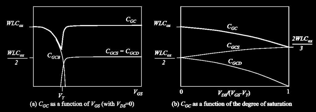
 1 EE 560 MOS TRANSISTOR THEORY PART nmos TRANSISTOR IN LINEAR REGION V S = 0 V G > V T0 channel SiO V D = small 4 C GC C BC substrate depletion region or bulk B p nmos TRANSISTOR AT EDGE OF SATURATION
The Devices. Devices
 The The MOS Transistor Gate Oxyde Gate Source n+ Polysilicon Drain n+ Field-Oxyde (SiO 2 ) p-substrate p+ stopper Bulk Contact CROSS-SECTION of NMOS Transistor Cross-Section of CMOS Technology MOS transistors