Nanometer Transistors and Their Models. Jan M. Rabaey
|
|
|
- Francine Parker
- 5 years ago
- Views:
Transcription

1 Nanometer Transistors and Their Models Jan M. Rabaey
2 Chapter Outline Nanometer transistor behavior and models Sub-threshold currents and leakage Variability Device and technology innovations
3 Nanometer Transistors and Their Models Emerging devices in the sub-100 nm regime post challenges to low-power design Leakage Variability Reliability Yet also offer some opportunities Increased mobility Improved control (?) State-of-the-art low-power design should build on and exploit these properties Requires clear understanding and good models
4 The Sub-100 nm Transistor Velocity-saturated Linear dependence between I D and V GS Threshold voltage V TH strongly impacted by channel length L and V DS Reduced threshold control through body biasing Leaky Sub-threshold leakage Gate leakage Decreasing I on over I off ratio
5 I D versus V DS for 65 nm bulk NMOS transistor I D (A) V GS = 1.0 V GS = 0.8 V GS = 0.6 V GS = 0.4 I D is a linear function of V GS V DS (V) Early saturation Decreased output resistance
6 Drain Current Under Velocity Saturation I DSat = v Sat WC ox (V GS V TH ) 2 V GS V TH + E C L Good model, could be used in hand or MATLAB analysis = W L μ C eff ox V V V ) 2 I DSat DSat ( GS TH with V DSat = ( V V ) E L V GS TH C GS VTH + EC L [Ref: Taur-Ning, 98]
7 Models for Sub-100 nm CMOS Transistors Further simplification: The unified model useful for hand analysis Assumes V DSat constant [Ref: Rabaey, DigIC 03]
8 Models for Sub-100 nm CMOS Transistors unified model simulation V linear 1.0V I DS [μa] vel. saturation 0.8V V saturation V V DSat V DS [V]
9 Alpha Power Law Model Alternate approach, useful for hand analysis of propagation delay I DS W = μ C 2 L ox V GS V Parameter α is between 1 and 2. In nm CMOS technology α ~ α TH This is not a physical model Simply empirical: Can fit (in minimum mean squares sense) to a variety of α s, V TH Need to find one with minimum square error fitted V TH can be different from physical [Ref: Sakurai, JSSC 90]
10 Output Resistance Drain current keeps increasing beyond the saturation point Slope in I V characteristics caused by: Channel-length modulation (CLM) Drain-induced barrier lowering (DIBL). The simulations show approximately linear dependence of I DS on V DS in saturation (modeled by λ factor) (kω) [Ref: BSIM 3v3 Manual]
11 Thresholds and Sub-Threshold Current 8.0E E 04 Drain current vs. gate source voltage V DS = 1.2 V I DS [A] 4.0E E E V THZ V GS [V]
12 Forward and Reverse Body Bias Threshold value can be adjusted through the fourth terminal, the transistor body. 0.5 Forward bias restricted by SB and DB junctions 0.45 V TH (V) Reverse bias Forward bias V BS (V)
13 Evolution of Threshold Control Body-biasing effect diminishes with technology scaling below 100 nm. No designer control at all in FD SOI technology nm mv ΔV TH (V) nm 65 nm 95 mv 55 mv V BB (V)
14 Impact of Channel Length on Threshold Voltages With halo implants Long-channel threshold V TH L min (for small values of V DS ) L V TH [V] Partial depletion of channel due to source and drain junctions larger in short-channel devices Channel Length [m] Simulated V TH of 90 nm technology
15 Impact of Channel Length on Threshold Voltages Normalized leakage current Length (nm) 50% increase in channel length decreases leakage current by almost a factor of 20 for 90 nm technology
16 Drain-Induced Barrier Lowering (DIBL) In a short-channel device, source drain distance is comparable to the depletion region widths, and the drain voltage can modulate the threshold V TH = V TH0 λ d V DS V TH Short channel V DS = 0.2V V DS = 1.2V Long channel Channel 0 (S) L (D)

17 MOS Transistor Leakage Components G Gate leakage S D Junction leakage D S leakage B(W)
18 Sub-threshold Leakage The transistor in weak inversion 3 V DS = 1.2V 4 G log I DS [log A] S C i C d Sub D 8 Sub-threshold slope S = kt/q ln10 (1+C d /C i ) V GS [V] Drain leakage current varies exponentially with V GS Sub-threshold swing S is ~ mv/decade

19 Impact of Reduced Threshold Voltages on Leakage four orders of magnitude 300 mv Leakage: sub-threshold current for V GS = 0
20 Sub-threshold Current Sub-threshold behavior can be modeled physically 2 VGS VTH VDS V = GS VTH W kt nkt q = kt q nkt q I DS 2nμCox e 1 e I Se 1 e L q VDS kt q 2 W kt where n is the slope factor ( 1, typically around 1.5) and I S = 2nμCox L q Very often expressed in base 10 VGS VTH S I DS = I S nvds S 1 for V DS > 100 mv kt where S = n ( ) ln(10), the sub-threshold swing, ranging between 60 mv and 100 mv q
21 Sub-threshold Current - Revisited Drain-Induced Barrier Lowering (DIBL) Threshold reduces approximately linearly with V DS V TH = V TH 0 λ V Body-Biasing Effect Threshold reduces approximately linearly with V BS V = V γ V Leading to: TH TH 0 d d DS BS γ nvds = S VGS VTH 0 + λdvds + dvbs S I DS IS Leakage is an exponential function of drain and bulk voltages
 exponential increase with V DS (DIBL) 3 10x in current technologies 0 0 0.1 0.2 0.3 0.4 0.5 0.")
22 Sub-threshold Current as a Function of V DS I D (A) λ d = 0.18 S = 100 mv/dec DIBL Two effects: diffusion current (like in bipolar transistor) exponential increase with V DS (DIBL) 3 10x in current technologies V DS (V) I D versus V DS for minimum size 65 nm NMOS transistor (V GS = 0)
 High electrical field between G and D causes tunneling and generation of electron hole pairs Causes current to flow between drain and bulk Involves many effects such as band-toband direct")
23 Gate-Induced Drain Leakage (GIDL) Excess drain current is observed, when gate voltage is moved below V TH, and moves to negative values (for NMOS) More pronounced for larger values of V DS (or GIDL ~ V DG ) High electrical field between G and D causes tunneling and generation of electron hole pairs Causes current to flow between drain and bulk Involves many effects such as band-toband direct tunneling and trap-assisted tunneling [Ref: J. Chen, TED 01] IEEE 2001
 10 8 GIDL V DS = 1.0 V V DS = 0.1 V 10 10 90 nm NMOS 10 12 0.4 0.2 0 0.")
24 Combining All Drain-Leakage Effects V DS = 2.5 V I D (A) 10 8 GIDL V DS = 1.0 V V DS = 0.1 V nm NMOS V GS (V)
25 Gate Leakage Introduction of high-k dielectrics Gate 1.2 nm SiO 2 Silicon substrate Scaling leads to gate-oxide thickness of a couple of molecules Causes gates to leak! MOS digital design has always been based on the assumption of infinite input resistance! Hence: Fundamental impact on design strategy! [Ref: K. Mistry, IEDM 07]
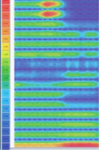
26 Gate-Leakage Mechanisms 1E 07 I 1E 08 ox /E 2 1E 09 A*cm 2 /MV 2 1E 10 1E 11 1E 12 1E 13 1E 14 1E 15 IEEE Å FN tunneling <50 Å Direct-oxide tunneling /E (MV/cm) Direct-oxide tunneling dominates for lower T ox [Ref: Chandrakasan-Bowhill, Ch3, 00]
27 10 9 T ox Direct-Oxide Tunneling Currents J G (A/cm 2 ) V DD trend nm 0.8 nm 1.0 nm 1.2 nm 1.5 nm 1.9 nm J G : exponential function of oxide thickness and applied voltage Vox 1 (1 ) ΦB α Vox / Tox J G e 3/2 V DD Also - Gate tunneling a strong function of temperature - Larger impact for NMOS than PMOS [Courtesy: S. Song, 01]
28 High-k Gate Dielectric T ox SiO 2 T g High-k Material Electrode Electrode Si substrate Si substrate Equivalent Oxide Thickness = EOT = T ox = T g * (3.9/ε g ), where 3.9 is relative permittivity of SiO 2 and ε g is relative permittivity of high-k material Currently SiO 2 /Ni; Candidate materials: HfO 2 ( ε eff ~15 30); HfSiO x ( ε eff ~12 16) Often combined with metal gate Reduced Gate Leakage for Similar Drive Current

29 High-k Dielectrics Gate 1.2 nm SiO 2 Gate electrode 3.0nm High-k Silicon substrate Silicon substrate High-k vs SiO 2 Benefits Gate capacitance Gate dielectric leakage 60% greater Faster transistors >100% reduction Lower power Buys a few generations of technology scaling [Courtesy: Intel]

30 Gate Leakage Current Density Limit Versus Simulated Gate Leakage [Ref: ITRS 2005]
31 Temperature Sensitivity Increasing temperature Reduces mobility Reduces V TH I on decreases with temperature I off increases with temperature I on /I off I DS nm NMOS Temp( C) increasing temperature V Gs
32 Variability Scaled device dimensions leading to increased impact of variations Device physics Manufacturing Temporal and environmental Impacts performance, power (mostly leakage) and manufacturing yield More pronounced in low-power design due to reduced supply/threshold voltage ratios
33 Variability Impacts Leakage 1.4 Normalized Frequency % 5X 130 nm Normalized Leakage (I( I sb ) Threshold variations have exponential impact on leakage [Ref: P. Gelsinger, DAC 04]
34 Variability Sources Physical Changes in characteristics of devices and wires. Caused by IC manufacturing process, device physics & wear-out (electro-migration). Time scale: 10 9 s (years). Environmental Changes in operational conditions (modes), V DD, temperature, local coupling. Caused by the specifics of the design implementation. Time scale: 10 6 to 10 9 s (clock tick).
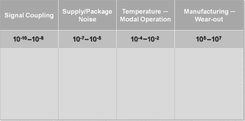
35 Variability Sources and Their Time Scales
36 Process Variations 3σ/mean 40% 30% 20% 10% 0% L eff w, h, ρ T ox, V TH Technology Node (nm) Percentage of total variation accounted for by within-die variation(device and interconnect) [Courtesy: S. Nassif, IBM] L (nm) V TH (mv) σ(v TH ) (mv) σ(v TH )/V TH 4.7% 5.8% 8.2% 9.3% 10.7% 16%
 Decrease of random dopants in channel increases impact of variations on threshold voltage [Courtesy: S.")
37 Threshold Variations Most Important for Power Mean Number of Dopant Atoms Technology Node (nm) Decrease of random dopants in channel increases impact of variations on threshold voltage [Courtesy: S. Borkar, Intel]
38 Device and Technology Innovations Power challenges introduced by nanometer MOS transistors can be partially addressed by new device structures and better materials Higher mobility Reduced leakage Better control However Most of these techniques provide only a one (or two) technology generation boost Need to be accompanied by circuit and system level methodologies


39 Device and Technology Innovations Strained silicon Silicon-on-Insulator Dual-gated devices Very high mobility devices MEMS transistors DG-SOI GP-SOI FinFET

40 Strained Silicon Improved ON-Current (10 25%) translates into: 84 97% leakage current reduction or 15% active power reduction [Ref: P. Gelsinger, DAC 04]
41 Strained Silicon Improves Transistor Performance and/or Reduces Leakage Transistor Leakage Current (na/μm) Std Strain Std Strain PMOS NMOS % I ON +10% I ON 0.04 I OFF Transistor Drive Current (ma/μm) [Ref: S. Chou, ISSCC 05] 0.20 I OFF
 Example: Si-Ge-Si heterostructure channel [Courtesy: G. Fitzgerald (MIT), K.")
42 Beyond Straining Hetero-junction devices allow for even larger carrier mobility Mobility (cm/s) Electrons (intrinsic) Si + strain ε Si Ge, GaAs InAs InSb Lattice Constant (Å) Example: Si-Ge-Si heterostructure channel [Courtesy: G. Fitzgerald (MIT), K. Saraswat (Stanford)]
![Silicon-on-Insulator (SOI) Thin silicon layer S G FD Thin Oxide Substrate D [Courtesy: IBM] Reduced capacitance (source and drain to bulk) results in lower dynamic power](/docs-images/83/87820815/images/43-2.jpg "Faster sub-threshold roll-off (close to 60 mv/decade) Random threshold fluctuations eliminated in fullydepleted SOI Reduced impact of soft-errors But More expensive Secondary")
43 Silicon-on-Insulator (SOI) Thin silicon layer S G FD Thin Oxide Substrate D [Courtesy: IBM] Reduced capacitance (source and drain to bulk) results in lower dynamic power Faster sub-threshold roll-off (close to 60 mv/decade) Random threshold fluctuations eliminated in fullydepleted SOI Reduced impact of soft-errors But More expensive Secondary effects
44 Example: Double-Gated Fully Depleted SOI thin BOX (< 10nm) VT control dopant (10 18 /cm 3 ) G (Ni silicide) thin SOI (< 20 nm) STI D well sub S STI well sub well contact STI Buried gate provides accurate threshold control over wide range Threshold voltage V TH (V) High dose Low dose w/o IEEE 2004 VDD = 1.0 V t SOI = 20 nm t BOX = 10 nm Well-bias voltage V well (V) nm bulk 65 nm bulk 45 nm bulk 32 nm bulk 65 nm FD-SOI 45 nm FD-SOI 32 nm FD-SOI [Ref: M. Yamaoka, VLSI 04, R. Tsuchiya, IEDM 04] 0 σ int σext σ int σext σ (V T) σ (VT) 1 2 Standard deviation (a.u.)


45 FinFETs An Entirely New Device Architecture IEEE 1999 UC Berkeley, 1999 Suppressed short-channel effects Higher on-current for reduced leakage Undoped channel No random dopant fluctuations [Ref: X. Huang, IEDM 99] S = 69 mv/decade
46 BackGated FinFET Source Gate length = L G Gate Fin Width = Drain T Si Fin Height H FIN = W /2 Source Switching Gate Gate length = Gate1 Drain L G Gate2 Vth Control Fin Height H FIN =W FIN Double-gated (DG) MOSFET Back-gated (BG) MOSFET Independent front and back gates One switching gate and V TH control gate Increased threshold control

47 New Transistors: FinFETs Intel tri-gate Berkeley PMOS FinFET Manufacturability still an issue may even cause more variations Source Gate Drain [Courtesy: T.J. King, UCB; Intel]
![Some Futuristic Devices FETs with sub-threshold swing < kt/q (I-MOS) Impact Ionization 1.0E 03 V S = 1V I-MOS Region ON Poly V D = 0V P + I-MOS Buried-Oxide [Courtesy: J. Plummer, Stanford] N + 1.](/docs-images/83/87820815/images/48-0.jpg "0E 05 MOS 1.0E 07 5 mv/dec. L I = 25 nm L G = 25 nm 1.0E 09 OFF T ox = 1 nm T si = 25 nm 1.0E 11 0 0.2 0.4 0.6 Zero off-current transistor Uses MEMS technology to physically change gate control.")
48 Some Futuristic Devices FETs with sub-threshold swing < kt/q (I-MOS) Impact Ionization 1.0E 03 V S = 1V I-MOS Region ON Poly V D = 0V P + I-MOS Buried-Oxide [Courtesy: J. Plummer, Stanford] N + 1.0E 05 MOS 1.0E 07 5 mv/dec. L I = 25 nm L G = 25 nm 1.0E 09 OFF T ox = 1 nm T si = 25 nm 1.0E Zero off-current transistor Uses MEMS technology to physically change gate control. Allows for zero-leakage sleep transistors and advanced memories [Ref: Abele05, Kam05] IEEE 2005
49 Summary Plenty of opportunity for scaling in the nanometer age Deep-submicron behavior of MOS transistors has substantial impact on design Power dissipation mostly influenced by increased leakage (SD and gate) and increasing impact of process variations Novel devices and materials will ensure scaling to a few nanometers
50 References Books and Book Chapters A. Chandrakasan, W. Bowhill, and F. Fox (eds.), Design of High-Performance Microprocessor Circuits, IEEE Press J. Rabaey, A. Chandrakasan, and B. Nikolic, Digital Integrated Circuits: A Design Perspective, 2nd ed, Prentice Hall Y. Taur and T.H. Ning, Fundamentals of Modern VLSI Devices, Cambridge University Press, Articles N. Abele, R. Fritschi, K. Boucart, F. Casset, P. Ancey, and A.M. Ionescu, Suspended-Gate MOSFET: Bringing New MEMS Functionality into Solid-State MOS Transistor, Proc. Electron Devices Meeting, IEDM Technical Digest. IEEE International, pp , Dec BSIM3V3 User Manual, J.H. Chen et al., An analytic three-terminal band-to-band tunneling model on GIDL in MOSFET, IEEE Trans. On Electron Devices, 48(7), pp , July S. Chou, Innovation and Integration in the Nanoelectronics Era, Digest ISSCC 2005, pp , February P. Gelsinger, Giga-scale Integration for Tera-Ops Performance, 41st DAC Keynote, DAC, 2004, ( X. Huang et al., "Sub 50-nm FinFET: PMOS, International Electron Devices Meeting Technical Digest, p. 67. Dec. 5 8, International Technology Roadmap for Semiconductors, H. Kam et al., A new nano-electro-mechanical field effect transistor (NEMFET) design for low-power electronics, IEDM Tech. Digest, pp , Dec K. Mistry et al., A 45nm Logic Technology with High-k+Metal Gate Transistors, Strained Silicon, 9 Cu Interconnect Layers, 193 nm Dry Patterning, and 100% Pb-free Packaging, Proceedings, IEDM, p. 247, Washington, Dec Predictive Technology Model (PTM), T. Sakurai and R. Newton. Alpha-power law MOSFET model and its applications to CMOS inverter delay and other formulas., IEEE Journal of Solid-State Circuits, 25(2), R. Tsuchiya et al., Silicon on thin BOX: a new paradigm of the CMOSFET for low-power high-performance application featuring wide-range back-bias control, Proceedings IEDM 2004, pp , Dec M. Yamaoka et al., Low power SRAM menu for SOC application using Yin-Yang-feedback memory cell technology, Digest of Technical Papers VLSI Symposium, pp , June W. Zhao, Y. Cao, New generation of predictive technology model for sub-45nm early design exploration, IEEE Transactions on Electron Devices, 53(11), pp , November 2006
The Devices. Digital Integrated Circuits A Design Perspective. Jan M. Rabaey Anantha Chandrakasan Borivoje Nikolic. July 30, 2002
 Digital Integrated Circuits A Design Perspective Jan M. Rabaey Anantha Chandrakasan Borivoje Nikolic The Devices July 30, 2002 Goal of this chapter Present intuitive understanding of device operation Introduction
Digital Integrated Circuits A Design Perspective. Jan M. Rabaey Anantha Chandrakasan Borivoje Nikolic. The Devices. July 30, Devices.
 Digital Integrated Circuits A Design Perspective Jan M. Rabaey Anantha Chandrakasan Borivoje Nikolic The July 30, 2002 1 Goal of this chapter Present intuitive understanding of device operation Introduction
CMPEN 411 VLSI Digital Circuits. Lecture 03: MOS Transistor
 CMPEN 411 VLSI Digital Circuits Lecture 03: MOS Transistor Kyusun Choi [Adapted from Rabaey s Digital Integrated Circuits, Second Edition, 2003 J. Rabaey, A. Chandrakasan, B. Nikolic] CMPEN 411 L03 S.1
EE5311- Digital IC Design
 EE5311- Digital IC Design Module 1 - The Transistor Janakiraman V Assistant Professor Department of Electrical Engineering Indian Institute of Technology Madras Chennai October 28, 2017 Janakiraman, IITM
Lecture 5: CMOS Transistor Theory
 Lecture 5: CMOS Transistor Theory Slides courtesy of Deming Chen Slides based on the initial set from David Harris CMOS VLSI Design Outline q q q q q q q Introduction MOS Capacitor nmos I-V Characteristics
The Devices. Digital Integrated Circuits A Design Perspective. Jan M. Rabaey Anantha Chandrakasan Borivoje Nikolic. July 30, 2002
 igital Integrated Circuits A esign Perspective Jan M. Rabaey Anantha Chandrakasan Borivoje Nikolic The evices July 30, 2002 Goal of this chapter Present intuitive understanding of device operation Introduction
Nanoscale CMOS Design Issues
 Nanoscale CMOS Design Issues Jaydeep P. Kulkarni Assistant Professor, ECE Department The University of Texas at Austin jaydeep@austin.utexas.edu Fall, 2017, VLSI-1 Class Transistor I-V Review Agenda Non-ideal
Device Models (PN Diode, MOSFET )
") Device Models (PN Diode, MOSFET ) Instructor: Steven P. Levitan steve@ece.pitt.edu TA: Gayatri Mehta, José Martínez Book: Digital Integrated Circuits: A Design Perspective; Jan Rabaey Lab Notes: Handed
Device Models (PN Diode, MOSFET ) Instructor: Steven P. Levitan steve@ece.pitt.edu TA: Gayatri Mehta, José Martínez Book: Digital Integrated Circuits: A Design Perspective; Jan Rabaey Lab Notes: Handed
MOSFET: Introduction
 E&CE 437 Integrated VLSI Systems MOS Transistor 1 of 30 MOSFET: Introduction Metal oxide semiconductor field effect transistor (MOSFET) or MOS is widely used for implementing digital designs Its major
Lecture 11: MOSFET Modeling
 Digital Integrated Circuits (83-313) Lecture 11: MOSFET ing Semester B, 2016-17 Lecturer: Dr. Adam Teman TAs: Itamar Levi, Robert Giterman 18 June 2017 Disclaimer: This course was prepared, in its entirety,
Device Models (PN Diode, MOSFET )
") Device Models (PN Diode, MOSFET ) Instructor: Steven P. Levitan steve@ece.pitt.edu TA: Gayatri Mehta, José Martínez Book: Digital Integrated Circuits: A Design Perspective; Jan Rabaey Lab Notes: Handed
Device Models (PN Diode, MOSFET ) Instructor: Steven P. Levitan steve@ece.pitt.edu TA: Gayatri Mehta, José Martínez Book: Digital Integrated Circuits: A Design Perspective; Jan Rabaey Lab Notes: Handed
A final review session will be offered on Thursday, May 10 from 10AM to 12noon in 521 Cory (the Hogan Room).
.") A final review session will be offered on Thursday, May 10 from 10AM to 12noon in 521 Cory (the Hogan Room). The Final Exam will take place from 12:30PM to 3:30PM on Saturday May 12 in 60 Evans.» All of
A final review session will be offered on Thursday, May 10 from 10AM to 12noon in 521 Cory (the Hogan Room). The Final Exam will take place from 12:30PM to 3:30PM on Saturday May 12 in 60 Evans.» All of
Impact of Scaling on The Effectiveness of Dynamic Power Reduction Schemes
 Impact of Scaling on The Effectiveness of Dynamic Power Reduction Schemes D. Duarte Intel Corporation david.e.duarte@intel.com N. Vijaykrishnan, M.J. Irwin, H-S Kim Department of CSE, Penn State University
MOS Transistor Theory
 CHAPTER 3 MOS Transistor Theory Outline 2 1. Introduction 2. Ideal I-V Characteristics 3. Nonideal I-V Effects 4. C-V Characteristics 5. DC Transfer Characteristics 6. Switch-level RC Delay Models MOS
EECS130 Integrated Circuit Devices
 EECS130 Integrated Circuit Devices Professor Ali Javey 10/30/2007 MOSFETs Lecture 4 Reading: Chapter 17, 19 Announcements The next HW set is due on Thursday. Midterm 2 is next week!!!! Threshold and Subthreshold
VLSI Design The MOS Transistor
 VLSI Design The MOS Transistor Frank Sill Torres Universidade Federal de Minas Gerais (UFMG), Brazil VLSI Design: CMOS Technology 1 Outline Introduction MOS Capacitor nmos I-V Characteristics pmos I-V
MOS Transistor I-V Characteristics and Parasitics
 ECEN454 Digital Integrated Circuit Design MOS Transistor I-V Characteristics and Parasitics ECEN 454 Facts about Transistors So far, we have treated transistors as ideal switches An ON transistor passes
The Future of CMOS. David Pulfrey. CHRONOLOGY of the FET. Lecture Lilienfeld s patent (BG FET) 1965 Commercialization (Fairchild)
 1965 Commercialization (Fairchild)") The Future of CMOS David Pulfrey 1 CHRONOLOGY of the FET 1933 Lilienfeld s patent (BG FET) 1965 Commercialization (Fairchild) 1991 The most abundant object made by mankind (C.T. Sah) 2003 The 10 nm FET
The Future of CMOS David Pulfrey 1 CHRONOLOGY of the FET 1933 Lilienfeld s patent (BG FET) 1965 Commercialization (Fairchild) 1991 The most abundant object made by mankind (C.T. Sah) 2003 The 10 nm FET
L ECE 4211 UConn F. Jain Scaling Laws for NanoFETs Chapter 10 Logic Gate Scaling
 L13 04202017 ECE 4211 UConn F. Jain Scaling Laws for NanoFETs Chapter 10 Logic Gate Scaling Scaling laws: Generalized scaling (GS) p. 610 Design steps p.613 Nanotransistor issues (page 626) Degradation
MOS Transistors. Prof. Krishna Saraswat. Department of Electrical Engineering Stanford University Stanford, CA
 MOS Transistors Prof. Krishna Saraswat Department of Electrical Engineering S Stanford, CA 94305 saraswat@stanford.edu 1 1930: Patent on the Field-Effect Transistor! Julius Lilienfeld filed a patent describing
Scaling Issues in Planar FET: Dual Gate FET and FinFETs
 Scaling Issues in Planar FET: Dual Gate FET and FinFETs Lecture 12 Dr. Amr Bayoumi Fall 2014 Advanced Devices (EC760) Arab Academy for Science and Technology - Cairo 1 Outline Scaling Issues for Planar
EE410 vs. Advanced CMOS Structures
 EE410 vs. Advanced CMOS Structures Prof. Krishna S Department of Electrical Engineering S 1 EE410 CMOS Structure P + poly-si N + poly-si Al/Si alloy LPCVD PSG P + P + N + N + PMOS N-substrate NMOS P-well
Integrated Circuits & Systems
 Federal University of Santa Catarina Center for Technology Computer Science & Electronics Engineering Integrated Circuits & Systems INE 5442 Lecture 10 MOSFET part 1 guntzel@inf.ufsc.br ual-well Trench-Isolated
A Multi-Gate CMOS Compact Model BSIMMG
 A Multi-Gate CMOS Compact Model BSIMMG Darsen Lu, Sriramkumar Venugopalan, Tanvir Morshed, Yogesh Singh Chauhan, Chung-Hsun Lin, Mohan Dunga, Ali Niknejad and Chenming Hu University of California, Berkeley
The Devices: MOS Transistors
 The Devices: MOS Transistors References: Semiconductor Device Fundamentals, R. F. Pierret, Addison-Wesley Digital Integrated Circuits: A Design Perspective, J. Rabaey et.al. Prentice Hall NMOS Transistor
Lecture 4: CMOS Transistor Theory
 Introduction to CMOS VLSI Design Lecture 4: CMOS Transistor Theory David Harris, Harvey Mudd College Kartik Mohanram and Steven Levitan University of Pittsburgh Outline q Introduction q MOS Capacitor q
The Devices. Jan M. Rabaey
 The Devices Jan M. Rabaey Goal of this chapter Present intuitive understanding of device operation Introduction of basic device equations Introduction of models for manual analysis Introduction of models
Multiple Gate CMOS and Beyond
 Multiple CMOS and Beyond Dept. of EECS, KAIST Yang-Kyu Choi Outline 1. Ultimate Scaling of MOSFETs - 3nm Nanowire FET - 8nm Non-Volatile Memory Device 2. Multiple Functions of MOSFETs 3. Summary 2 CMOS
CHAPTER 5 EFFECT OF GATE ELECTRODE WORK FUNCTION VARIATION ON DC AND AC PARAMETERS IN CONVENTIONAL AND JUNCTIONLESS FINFETS
 98 CHAPTER 5 EFFECT OF GATE ELECTRODE WORK FUNCTION VARIATION ON DC AND AC PARAMETERS IN CONVENTIONAL AND JUNCTIONLESS FINFETS In this chapter, the effect of gate electrode work function variation on DC
CMOS INVERTER. Last Lecture. Metrics for qualifying digital circuits. »Cost» Reliability» Speed (delay)»performance
»performance") CMOS INVERTER Last Lecture Metrics for qualifying digital circuits»cost» Reliability» Speed (delay)»performance 1 Today s lecture The CMOS inverter at a glance An MOS transistor model for manual analysis
CMOS INVERTER Last Lecture Metrics for qualifying digital circuits»cost» Reliability» Speed (delay)»performance 1 Today s lecture The CMOS inverter at a glance An MOS transistor model for manual analysis
Today s lecture. EE141- Spring 2003 Lecture 4. Design Rules CMOS Inverter MOS Transistor Model
 - Spring 003 Lecture 4 Design Rules CMOS Inverter MOS Transistor Model Today s lecture Design Rules The CMOS inverter at a glance An MOS transistor model for manual analysis Important! Labs start next
Microelectronics Part 1: Main CMOS circuits design rules
 GBM8320 Dispositifs Médicaux telligents Microelectronics Part 1: Main CMOS circuits design rules Mohamad Sawan et al. Laboratoire de neurotechnologies Polystim! http://www.cours.polymtl.ca/gbm8320/! med-amine.miled@polymtl.ca!
III-V CMOS: What have we learned from HEMTs? J. A. del Alamo, D.-H. Kim 1, T.-W. Kim, D. Jin, and D. A. Antoniadis
 III-V CMOS: What have we learned from HEMTs? J. A. del Alamo, D.-H. Kim 1, T.-W. Kim, D. Jin, and D. A. Antoniadis Microsystems Technology Laboratories, MIT 1 presently with Teledyne Scientific 23rd International
MSE 310/ECE 340: Electrical Properties of Materials Fall 2014 Department of Materials Science and Engineering Boise State University
 MSE 310/ECE 340: Electrical Properties of Materials Fall 2014 Department of Materials Science and Engineering Boise State University Practice Final Exam 1 Read the questions carefully Label all figures
Chapter 5 MOSFET Theory for Submicron Technology
 Chapter 5 MOSFET Theory for Submicron Technology Short channel effects Other small geometry effects Parasitic components Velocity saturation/overshoot Hot carrier effects ** Majority of these notes are
FLCC Seminar. Spacer Lithography for Reduced Variability in MOSFET Performance
 1 Seminar Spacer Lithography for Reduced Variability in MOSFET Performance Prof. Tsu-Jae King Liu Electrical Engineering & Computer Sciences Dept. University of California at Berkeley Graduate Student:
ESE 570: Digital Integrated Circuits and VLSI Fundamentals
 ESE 570: Digital Integrated Circuits and VLSI Fundamentals Lec 4: January 23, 2018 MOS Transistor Theory, MOS Model Penn ESE 570 Spring 2018 Khanna Lecture Outline! CMOS Process Enhancements! Semiconductor
ECE 497 JS Lecture - 12 Device Technologies
 ECE 497 JS Lecture - 12 Device Technologies Spring 2004 Jose E. Schutt-Aine Electrical & Computer Engineering University of Illinois jose@emlab.uiuc.edu 1 NMOS Transistor 2 ρ Source channel charge density
Technische Universität Graz. Institute of Solid State Physics. 11. MOSFETs
 Technische Universität Graz Institute of Solid State Physics 11. MOSFETs Dec. 12, 2018 Gradual channel approximation accumulation depletion inversion http://lampx.tugraz.at/~hadley/psd/l10/gradualchannelapprox.php
Enhanced Mobility CMOS
 Enhanced Mobility CMOS Judy L. Hoyt I. Åberg, C. Ni Chléirigh, O. Olubuyide, J. Jung, S. Yu, E.A. Fitzgerald, and D.A. Antoniadis Microsystems Technology Laboratory MIT, Cambridge, MA 02139 Acknowledge
Practice 3: Semiconductors
 Practice 3: Semiconductors Digital Electronic Circuits Semester A 2012 VLSI Fabrication Process VLSI Very Large Scale Integration The ability to fabricate many devices on a single substrate within a given
6.012 Electronic Devices and Circuits
 Page 1 of 10 YOUR NAME Department of Electrical Engineering and Computer Science Massachusetts Institute of Technology 6.012 Electronic Devices and Circuits Exam No. 2 Thursday, November 5, 2009 7:30 to
Status. Embedded System Design and Synthesis. Power and temperature Definitions. Acoustic phonons. Optic phonons
 Status http://robertdick.org/esds/ Office: EECS 2417-E Department of Electrical Engineering and Computer Science University of Michigan Specification, languages, and modeling Computational complexity,
MOS Transistor Theory
 MOS Transistor Theory So far, we have viewed a MOS transistor as an ideal switch (digital operation) Reality: less than ideal EE 261 Krish Chakrabarty 1 Introduction So far, we have treated transistors
Chapter 4 Field-Effect Transistors
 Chapter 4 Field-Effect Transistors Microelectronic Circuit Design Richard C. Jaeger Travis N. Blalock 5/5/11 Chap 4-1 Chapter Goals Describe operation of MOSFETs. Define FET characteristics in operation
EE105 Fall 2014 Microelectronic Devices and Circuits. NMOS Transistor Capacitances: Saturation Region
 EE105 Fall 014 Microelectronic Devices and Circuits Prof. Ming C. Wu wu@eecs.berkeley.edu 511 Sutardja Dai Hall (SDH) 1 NMOS Transistor Capacitances: Saturation Region Drain no longer connected to channel
Semiconductor Physics Problems 2015
 Semiconductor Physics Problems 2015 Page and figure numbers refer to Semiconductor Devices Physics and Technology, 3rd edition, by SM Sze and M-K Lee 1. The purest semiconductor crystals it is possible
Lecture 3: CMOS Transistor Theory
 Lecture 3: CMOS Transistor Theory Outline Introduction MOS Capacitor nmos I-V Characteristics pmos I-V Characteristics Gate and Diffusion Capacitance 2 Introduction So far, we have treated transistors
Scaling of MOS Circuits. 4. International Technology Roadmap for Semiconductors (ITRS) 6. Scaling factors for device parameters
 6. Scaling factors for device parameters") 1 Scaling of MOS Circuits CONTENTS 1. What is scaling?. Why scaling? 3. Figure(s) of Merit (FoM) for scaling 4. International Technology Roadmap for Semiconductors (ITRS) 5. Scaling models 6. Scaling factors
1 Scaling of MOS Circuits CONTENTS 1. What is scaling?. Why scaling? 3. Figure(s) of Merit (FoM) for scaling 4. International Technology Roadmap for Semiconductors (ITRS) 5. Scaling models 6. Scaling factors
High Mobility Materials and Novel Device Structures for High Performance Nanoscale MOSFETs
 High Mobility Materials and Novel Device Structures for High Performance Nanoscale MOSFETs Prof. (Dr.) Tejas Krishnamohan Department of Electrical Engineering Stanford University, CA & Intel Corporation
EEC 118 Lecture #2: MOSFET Structure and Basic Operation. Rajeevan Amirtharajah University of California, Davis Jeff Parkhurst Intel Corporation
 EEC 118 Lecture #2: MOSFET Structure and Basic Operation Rajeevan Amirtharajah University of California, Davis Jeff Parkhurst Intel Corporation Announcements Lab 1 this week, report due next week Bring
Semiconductor Physics fall 2012 problems
 Semiconductor Physics fall 2012 problems 1. An n-type sample of silicon has a uniform density N D = 10 16 atoms cm -3 of arsenic, and a p-type silicon sample has N A = 10 15 atoms cm -3 of boron. For each
Journal of Electron Devices, Vol. 18, 2013, pp JED [ISSN: ]
![Journal of Electron Devices, Vol. 18, 2013, pp JED [ISSN: ]](/thumbs/86/93990983.jpg "Journal of Electron Devices, Vol. 18, 2013, pp JED [ISSN: ]") DrainCurrent-Id in linearscale(a/um) Id in logscale Journal of Electron Devices, Vol. 18, 2013, pp. 1582-1586 JED [ISSN: 1682-3427 ] SUITABILITY OF HIGH-k GATE DIELECTRICS ON THE DEVICE PERFORMANCE AND
DrainCurrent-Id in linearscale(a/um) Id in logscale Journal of Electron Devices, Vol. 18, 2013, pp. 1582-1586 JED [ISSN: 1682-3427 ] SUITABILITY OF HIGH-k GATE DIELECTRICS ON THE DEVICE PERFORMANCE AND
CMPEN 411 VLSI Digital Circuits. Lecture 04: CMOS Inverter (static view)
") CMPEN 411 VLSI Digital Circuits Lecture 04: CMOS Inverter (static view) Kyusun Choi [Adapted from Rabaey s Digital Integrated Circuits, Second Edition, 2003 J. Rabaey, A. Chandrakasan, B. Nikolic] CMPEN
CMPEN 411 VLSI Digital Circuits Lecture 04: CMOS Inverter (static view) Kyusun Choi [Adapted from Rabaey s Digital Integrated Circuits, Second Edition, 2003 J. Rabaey, A. Chandrakasan, B. Nikolic] CMPEN
Introduction and Background
 Analog CMOS Integrated Circuit Design Introduction and Background Dr. Jawdat Abu-Taha Department of Electrical and Computer Engineering Islamic University of Gaza jtaha@iugaza.edu.ps 1 Marking Assignments
ECE 546 Lecture 10 MOS Transistors
 ECE 546 Lecture 10 MOS Transistors Spring 2018 Jose E. Schutt-Aine Electrical & Computer Engineering University of Illinois jesa@illinois.edu NMOS Transistor NMOS Transistor N-Channel MOSFET Built on p-type
Part 5: Quantum Effects in MOS Devices
 Quantum Effects Lead to Phenomena such as: Ultra Thin Oxides Observe: High Leakage Currents Through the Oxide - Tunneling Depletion in Poly-Si metal gate capacitance effect Thickness of Inversion Layer
The Inverter. Digital Integrated Circuits A Design Perspective. Jan M. Rabaey Anantha Chandrakasan Borivoje Nikolic
 Digital Integrated Circuits A Design Perspective Jan M. Rabaey Anantha Chandrakasan Borivoje Nikolic The Inverter Revised from Digital Integrated Circuits, Jan M. Rabaey el, 2003 Propagation Delay CMOS
ESE 570: Digital Integrated Circuits and VLSI Fundamentals
 ESE 570: Digital Integrated Circuits and VLSI Fundamentals Lec 4: January 29, 2019 MOS Transistor Theory, MOS Model Penn ESE 570 Spring 2019 Khanna Lecture Outline! CMOS Process Enhancements! Semiconductor
Future trends in radiation hard electronics
 Future trends in radiation hard electronics F. Faccio CERN, Geneva, Switzerland Outline Radiation effects in CMOS technologies Deep submicron CMOS for radiation environments What is the future going to
The Intrinsic Silicon
 The Intrinsic ilicon Thermally generated electrons and holes Carrier concentration p i =n i ni=1.45x10 10 cm-3 @ room temp Generally: n i = 3.1X10 16 T 3/2 e -1.21/2KT cm -3 T= temperature in K o (egrees
A Leakage Control System for Thermal Stability During Burn-In Test
 A Leakage Control System for Thermal Stability During Burn-In Test Mesut Meterelliyoz, Hamid Mahmoodi, and Kaushik Roy School of Electrical and Computer Engineering, Purdue University, West Lafayette,
Lecture 04 Review of MOSFET
 ECE 541/ME 541 Microelectronic Fabrication Techniques Lecture 04 Review of MOSFET Zheng Yang (ERF 3017, email: yangzhen@uic.edu) What is a Transistor? A Switch! An MOS Transistor V GS V T V GS S Ron D
S=0.7 [0.5x per 2 nodes] ESE370: Circuit-Level Modeling, Design, and Optimization for Digital Systems. Today. Scaling ITRS Roadmap
![S=0.7 [0.5x per 2 nodes] ESE370: Circuit-Level Modeling, Design, and Optimization for Digital Systems. Today. Scaling ITRS Roadmap](/thumbs/92/110446830.jpg "S=0.7 [0.5x per 2 nodes] ESE370: Circuit-Level Modeling, Design, and Optimization for Digital Systems. Today. Scaling ITRS Roadmap") ESE370: Circuit-Level Modeling, Design, and Optimization for Digital Systems Day 15: October 4, 2013 Scaling Today VLSI Scaling Trends/Disciplines Effects Alternatives (cheating) 1 2 Scaling ITRS Roadmap
ESE370: Circuit-Level Modeling, Design, and Optimization for Digital Systems Day 15: October 4, 2013 Scaling Today VLSI Scaling Trends/Disciplines Effects Alternatives (cheating) 1 2 Scaling ITRS Roadmap
ECE 342 Electronic Circuits. 3. MOS Transistors
 ECE 342 Electronic Circuits 3. MOS Transistors Jose E. Schutt-Aine Electrical & Computer Engineering University of Illinois jschutt@emlab.uiuc.edu 1 NMOS Transistor Typically L = 0.1 to 3 m, W = 0.2 to
ECE-305: Fall 2017 MOS Capacitors and Transistors
 ECE-305: Fall 2017 MOS Capacitors and Transistors Pierret, Semiconductor Device Fundamentals (SDF) Chapters 15+16 (pp. 525-530, 563-599) Professor Peter Bermel Electrical and Computer Engineering Purdue
EE241 - Spring 2005 Advanced Digital Integrated Circuits. Admin. Lecture 10: Power Intro
 EE241 - Spring 2005 Advanced Digital Integrated Circuits Lecture 10: Power Intro Admin Project Phase 2 due Monday March 14, 5pm (by e-mail to jan@eecs.berkeley.edu and huifangq@eecs.berkeley.edu) Should
Beyond Si: Opportunities and Challenges for CMOS Technology Based on High-Mobility Channel Materials T.P. Ma Yale University
 Beyond Si: Opportunities and Challenges for CMOS Technology Based on High-Mobility Channel Materials T.P. Ma Yale University Acknowledgments: Abigail Lubow, Xiao Sun, Shufeng Ren Switching Speed of CMOS
FIELD-EFFECT TRANSISTORS
 FIEL-EFFECT TRANSISTORS 1 Semiconductor review 2 The MOS capacitor 2 The enhancement-type N-MOS transistor 3 I-V characteristics of enhancement MOSFETS 4 The output characteristic of the MOSFET in saturation
Announcements. EE141- Fall 2002 Lecture 7. MOS Capacitances Inverter Delay Power
 - Fall 2002 Lecture 7 MOS Capacitances Inverter Delay Power Announcements Wednesday 12-3pm lab cancelled Lab 4 this week Homework 2 due today at 5pm Homework 3 posted tonight Today s lecture MOS capacitances
EE105 - Fall 2006 Microelectronic Devices and Circuits
 EE105 - Fall 2006 Microelectronic Devices and Circuits Prof. Jan M. Rabaey (jan@eecs) Lecture 7: MOS Transistor Some Administrative Issues Lab 2 this week Hw 2 due on We Hw 3 will be posted same day MIDTERM
CSE493/593. Designing for Low Power
 CSE493/593 Designing for Low Power Mary Jane Irwin [Adapted from Rabaey s Digital Integrated Circuits, 2002, J. Rabaey et al.].1 Why Power Matters Packaging costs Power supply rail design Chip and system
Lecture 6 Power Zhuo Feng. Z. Feng MTU EE4800 CMOS Digital IC Design & Analysis 2010
 EE4800 CMOS Digital IC Design & Analysis Lecture 6 Power Zhuo Feng 6.1 Outline Power and Energy Dynamic Power Static Power 6.2 Power and Energy Power is drawn from a voltage source attached to the V DD
Fig. 1 CMOS Transistor Circuits (a) Inverter Out = NOT In, (b) NOR-gate C = NOT (A or B)
 Inverter Out = NOT In, (b) NOR-gate C = NOT (A or B)") 1 Introduction to Transistor-Level Logic Circuits 1 By Prawat Nagvajara At the transistor level of logic circuits, transistors operate as switches with the logic variables controlling the open or closed
1 Introduction to Transistor-Level Logic Circuits 1 By Prawat Nagvajara At the transistor level of logic circuits, transistors operate as switches with the logic variables controlling the open or closed
The Devices. Devices
 The The MOS Transistor Gate Oxyde Gate Source n+ Polysilicon Drain n+ Field-Oxyde (SiO 2 ) p-substrate p+ stopper Bulk Contact CROSS-SECTION of NMOS Transistor Cross-Section of CMOS Technology MOS transistors
! CMOS Process Enhancements. ! Semiconductor Physics. " Band gaps. " Field Effects. ! MOS Physics. " Cut-off. " Depletion.
 ESE 570: Digital Integrated Circuits and VLSI Fundamentals Lec 4: January 3, 018 MOS Transistor Theory, MOS Model Lecture Outline! CMOS Process Enhancements! Semiconductor Physics " Band gaps " Field Effects!
Digital Integrated Circuits A Design Perspective
 Semiconductor Memories Adapted from Chapter 12 of Digital Integrated Circuits A Design Perspective Jan M. Rabaey et al. Copyright 2003 Prentice Hall/Pearson Outline Memory Classification Memory Architectures
CMOS Inverter (static view)
") Review: Design Abstraction Levels SYSTEM CMOS Inverter (static view) + MODULE GATE [Adapted from Chapter 5. 5.3 CIRCUIT of G DEVICE Rabaey s Digital Integrated Circuits,, J. Rabaey et al.] S D Review:
Review: Design Abstraction Levels SYSTEM CMOS Inverter (static view) + MODULE GATE [Adapted from Chapter 5. 5.3 CIRCUIT of G DEVICE Rabaey s Digital Integrated Circuits,, J. Rabaey et al.] S D Review:
MOS Transistor Theory MOSFET Symbols Current Characteristics of MOSFET. MOS Symbols and Characteristics. nmos Enhancement Transistor
 MOS Transistor Theory MOSFET Symbols Current Characteristics of MOSFET Calculation of t and Important 2 nd Order Effects SmallSignal Signal MOSFET Model Summary Material from: CMOS LSI Design By Weste
Part 4: Heterojunctions - MOS Devices. MOSFET Current Voltage Characteristics
 MOS Device Uses: Part 4: Heterojunctions - MOS Devices MOSCAP capacitor: storing charge, charge-coupled device (CCD), etc. MOSFET transistor: switch, current amplifier, dynamic random access memory (DRAM-volatile),
ECE 342 Electronic Circuits. Lecture 6 MOS Transistors
 ECE 342 Electronic Circuits Lecture 6 MOS Transistors Jose E. Schutt-Aine Electrical & Computer Engineering University of Illinois jesa@illinois.edu 1 NMOS Transistor Typically L = 0.1 to 3 m, W = 0.2
Homework 2 due on Wednesday Quiz #2 on Wednesday Midterm project report due next Week (4 pages)
") EE241 - Spring 2013 Advanced Digital Integrated Circuits Lecture 12: SRAM Design ECC Timing Announcements Homework 2 due on Wednesday Quiz #2 on Wednesday Midterm project report due next Week (4 pages)
EE241 - Spring 2013 Advanced Digital Integrated Circuits Lecture 12: SRAM Design ECC Timing Announcements Homework 2 due on Wednesday Quiz #2 on Wednesday Midterm project report due next Week (4 pages)
Introduction to CMOS VLSI. Chapter 2: CMOS Transistor Theory. Harris, 2004 Updated by Li Chen, Outline
 Introduction to MOS VLSI Design hapter : MOS Transistor Theory copyright@david Harris, 004 Updated by Li hen, 010 Outline Introduction MOS apacitor nmos IV haracteristics pmos IV haracteristics Gate and
Semiconductor Memories
 Semiconductor References: Adapted from: Digital Integrated Circuits: A Design Perspective, J. Rabaey UCB Principles of CMOS VLSI Design: A Systems Perspective, 2nd Ed., N. H. E. Weste and K. Eshraghian
EE115C Winter 2017 Digital Electronic Circuits. Lecture 3: MOS RC Model, CMOS Manufacturing
 EE115C Winter 2017 Digital Electronic Circuits Lecture 3: MOS RC Model, CMOS Manufacturing Agenda MOS Transistor: RC Model (pp. 104-113) S R on D CMOS Manufacturing Process (pp. 36-46) S S C GS G G C GD
Non Ideal Transistor Behavior
 Non Ideal Transistor Behavior Slides adapted from: N. Weste, D. Harris, CMOS VLSI Design, Addison- Wesley, 3/e, 2004 1 Non-ideal Transistor I-V effects Non ideal transistor Behavior Channel Length ModulaJon
Modeling and Computation of Gate Tunneling Current through Ultra Thin Gate Oxides in Double Gate MOSFETs with Ultra Thin Body Silicon Channel
 Modeling and Computation of Gate Tunneling Current through Ultra Thin Gate Oxides in Double Gate MOSFETs with Ultra Thin Body Silicon Channel Bhadrinarayana L V 17 th July 2008 Microelectronics Lab, Indian
CMPEN 411 VLSI Digital Circuits Spring 2012
 CMPEN 411 VLSI Digital Circuits Spring 2012 Lecture 09: Resistance & Inverter Dynamic View [Adapted from Rabaey s Digital Integrated Circuits, Second Edition, 2003 J. Rabaey, A. Chandrakasan, B. Nikolic]
The Critical Role of Quantum Capacitance in Compact Modeling of Nano-Scaled and Nanoelectronic Devices
 The Critical Role of Quantum Capacitance in Compact Modeling of Nano-Scaled and Nanoelectronic Devices Zhiping Yu and Jinyu Zhang Institute of Microelectronics Tsinghua University, Beijing, China yuzhip@tsinghua.edu.cn
Quarter-micrometre surface and buried channel PMOSFET modelling for circuit simulation
 Semicond. Sci. Technol. 11 1996) 1763 1769. Printed in the UK Quarter-micrometre surface and buried channel PMOSFET modelling for circuit simulation Yuhua Cheng, Min-chie Jeng, Zhihong Liu, Kai Chen, Bin
SECTION: Circle one: Alam Lundstrom. ECE 305 Exam 5 SOLUTIONS: Spring 2016 April 18, 2016 M. A. Alam and M.S. Lundstrom Purdue University
 NAME: PUID: SECTION: Circle one: Alam Lundstrom ECE 305 Exam 5 SOLUTIONS: April 18, 2016 M A Alam and MS Lundstrom Purdue University This is a closed book exam You may use a calculator and the formula
Objective and Outline. Acknowledgement. Objective: Power Components. Outline: 1) Acknowledgements. Section 4: Power Components
 Acknowledgements. Section 4: Power Components") Objective: Power Components Outline: 1) Acknowledgements 2) Objective and Outline 1 Acknowledgement This lecture note has been obtained from similar courses all over the world. I wish to thank all the
Objective: Power Components Outline: 1) Acknowledgements 2) Objective and Outline 1 Acknowledgement This lecture note has been obtained from similar courses all over the world. I wish to thank all the
Design/Technology Co-Optimisation (DTCO) in the Presence of Acute Variability
 in the Presence of Acute Variability") Design/Technology Co-Optimisation (DTCO) in the Presence of Acute Variability A. Asenov 1,2, E. A. Towie 1!! 1 Gold Standard Simulations Ltd 2 Glasgow University! Summary!! Introduction!! FinFET complexity
Design/Technology Co-Optimisation (DTCO) in the Presence of Acute Variability A. Asenov 1,2, E. A. Towie 1!! 1 Gold Standard Simulations Ltd 2 Glasgow University! Summary!! Introduction!! FinFET complexity
Recent Development of FinFET Technology for CMOS Logic and Memory
 Recent Development of FinFET Technology for CMOS Logic and Memory Chung-Hsun Lin EECS Department University of California at Berkeley Why FinFET Outline FinFET process Unique features of FinFET Mobility,
! CMOS Process Enhancements. ! Semiconductor Physics. " Band gaps. " Field Effects. ! MOS Physics. " Cut-off. " Depletion.
 ESE 570: Digital Integrated Circuits and VLSI Fundamentals Lec 4: January 9, 019 MOS Transistor Theory, MOS Model Lecture Outline CMOS Process Enhancements Semiconductor Physics Band gaps Field Effects
EECS240 Spring Today s Lecture. Lecture 2: CMOS Technology and Passive Devices. Lingkai Kong EECS. EE240 CMOS Technology
 EECS240 Spring 2013 Lecture 2: CMOS Technology and Passive Devices Lingkai Kong EECS Today s Lecture EE240 CMOS Technology Passive devices Motivation Resistors Capacitors (Inductors) Next time: MOS transistor
Lecture 15 OUTLINE. MOSFET structure & operation (qualitative) Review of electrostatics The (N)MOS capacitor
 Review of electrostatics The (N)MOS capacitor") Lecture 15 OUTLINE MOSFET structure & operation (qualitative) Review of electrostatics The (N)MOS capacitor Electrostatics Charge vs. voltage characteristic Reading: Chapter 6.1 6.2.1 EE15 Spring 28 Lecture
Lecture 15 OUTLINE MOSFET structure & operation (qualitative) Review of electrostatics The (N)MOS capacitor Electrostatics Charge vs. voltage characteristic Reading: Chapter 6.1 6.2.1 EE15 Spring 28 Lecture
ESE570 Spring University of Pennsylvania Department of Electrical and System Engineering Digital Integrated Cicruits AND VLSI Fundamentals
 University of Pennsylvania Department of Electrical and System Engineering Digital Integrated Cicruits AND VLSI Fundamentals ESE570, Spring 2018 Final Monday, Apr 0 5 Problems with point weightings shown.
Lecture #27. The Short Channel Effect (SCE)
") Lecture #27 ANNOUNCEMENTS Design Project: Your BJT design should meet the performance specifications to within 10% at both 300K and 360K. ( β dc > 45, f T > 18 GHz, V A > 9 V and V punchthrough > 9 V )
Lecture #27 ANNOUNCEMENTS Design Project: Your BJT design should meet the performance specifications to within 10% at both 300K and 360K. ( β dc > 45, f T > 18 GHz, V A > 9 V and V punchthrough > 9 V )
EEC 116 Lecture #3: CMOS Inverters MOS Scaling. Rajeevan Amirtharajah University of California, Davis Jeff Parkhurst Intel Corporation
 EEC 116 Lecture #3: CMOS Inverters MOS Scaling Rajeevan Amirtharajah University of California, Davis Jeff Parhurst Intel Corporation Outline Review: Inverter Transfer Characteristics Lecture 3: Noise Margins,