ESE370: Circuit-Level Modeling, Design, and Optimization for Digital Systems
|
|
|
- Rolf Bryan
- 5 years ago
- Views:
Transcription
1 ESE370: Circuit-Level Modeling, Design, and Optimization for Digital Systems Lec 12: October 4, 2017 Scaling Penn ESE 370 Fall Khanna
2 Today! VLSI Scaling Trends/Disciplines! Effects! Alternatives (cheating) Penn ESE 370 Fall Khanna 2
3 Scaling! Premise: features scale uniformly " everything gets better in a predictable manner! Parameters: # λ (lambda) -- Mead and Conway (Day14) # F -- Half pitch ITRS (F=2λ) # S scale factor Rabaey # F =S F Penn ESE 370 Fall Khanna 3
4 ITRS Roadmap! International Technology Roadmap for Semiconductors " Try to predict where industry going! ITRS 2.0 started in 2015 with new focus " System Integration, Heterogeneous Integration, Heterogeneous Components, Outside System Connectiviy, More Moore, Beyond CMOS and Factory Integartion.! Penn ESE 370 Fall Khanna 4

5 Microprocessor Trans Count Curve shows transistor count doubling every two years Pentium 2-Core Itanium 2 Pentium 4 Pentium III Pentium II AMD K5 16-Core SPARC T3 6-Core i7 i7 AMD K10 AMD K7 AMD K8 10-Core Xenon IBM 4-Core z196 IBM 8-Core POWER7 4-Core Itanium Tukwilla AMD 6-Core Opteron 4-Core i Mot Mot Zilog Z80 MOS : Oracle SPARC M7, 20 nm CMOS, 32-Core, 10B 3-D FinFET transistors. Kenneth R. Laker, University of Pennsylvania, updated 20Jan15 Penn ESE 370 Fall Khanna

6 Trend Minimum Feature Size vs. Year 100 µm 10 µm 1 µm 0.1 µm Process Node/ Minimum Feature 0.18 µm in 1999 Integrated Circuit History ITRS Roadmap 10 nm 1 nm Transition Region Quantum Devices NOT SO Distant Future 0.1 nm Atomic Dimensions Year Minimum Feature Measure = line/gate conductor width or half-pitch (adjacent 1 st metal layer lines or adjacent transistor gates) Penn ESE 370 Fall Khanna 6
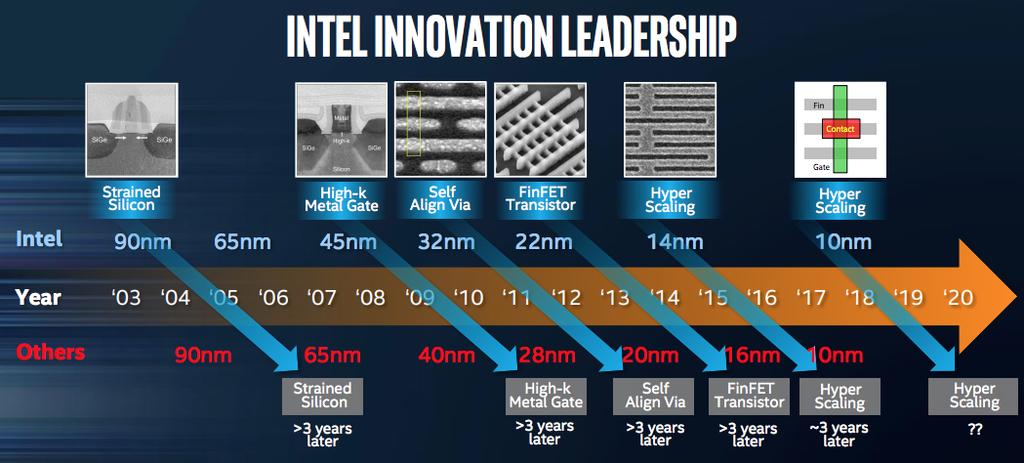
7 Intel Cost Scaling Penn ESE 370 Fall Khanna 7

8 Moore s Law Impact on Intel ucomputers Min Feature Size 2BT µp (Intel Itanium Tukwila) 4-Core chip (65 nm) introduced Q BT mp (Intel Itanium Poulson) 8-Core chip (32 nm) to be introduced Serial data links operating at 10 Gbits/sec. Introduces 22 nm Tri-gate Transistor Tech. Increased reuse of logic IP, i.e. designs and cores. Complexity - # transistors Double every Two Years Penn ESE 370 Fall Khanna 0.032um um YEAR 8
9 More Moore $ Scaling! Geometrical Scaling " continued shrinking of horizontal and vertical physical feature sizes! Equivalent Scaling " 3-dimensional device structure improvements and new materials that affect the electrical performance of the chip even if no geometrical scaling! Design Equivalent Scaling " design technologies that enable high performance, low power, high reliability, low cost, and high design productivity even if neither geometrical nor equivalent scaling can be used Penn ESE 370 Fall Khanna 9


10 22nm 3D FinFET Transistor High-k gate dielectric Tri-Gate transistors with multiple fins connected together increases total drive strength for higher performance Penn ESE 370 Fall Khanna 10

11 Scaling More-than-Moore More-than-Moore, International Road Map (IRC) White Paper, International Technology Road Map for Semiconductors Penn ESE 370 Fall Khanna 11

12 Semiconductor System Integration More Than Moore's Law Transistors/cm SOP law for system integration. As components shrink and boards all but disappear, component density will double every year or so. Multichip Module Systemin-package (SIP) System on-package (SOP) Components/cm R. Tummala, Moore's Law Meets Its Match, IEEE Spectrum, June, 2006 Penn ESE 370 Fall Khanna 12
13 Improvement Trends for VLSI SoCs Enabled by Geometrical and Equivalent Scaling! TRENDS:! Higher Integration level " exponentially increased number of components/ transistors per chip/package.! Performance Scaling " combination of Geometrical (shrinking of dimensions) and Equivalent (innovation) Scaling.! System implementation " SoC + increased use of SiP - > SOP! CONSEQUENCES:! Higher Speed " CPU clock rate at multiple GHz + parallel processing.! Increased Compactness & less weight " increasing system integration.! Lower Power " Decreasing energy requirement per function.! Lower Cost " Decreasing cost per function. Penn ESE 370 Fall Khanna 13

14 Societal Needs Penn ESE 370 Fall Khanna 14
15 More Moore $ Scaling! Examples: " Design-for-variability " Low power design (sleep modes, clock gating, multi- Vdd, etc.) " Multi-core SOC architectures Penn ESE 370 Fall Khanna 15
16 Preclass 1! Scaling from 32nm $ 22nm? " Scaling minimum gate length " And pitch distance Penn ESE 370 Fall Khanna 16
17 Half Pitch (= Pitch/2) Definition Metal Pitch Poly Pitch (Typical DRAM) (Typical MPU/ASIC) Source: 2001 ITRS - Exec. Summary, ORTC Figure, Andrew Kahng Penn ESE 370 Fall Khanna 17
18 MOS Transistor Scaling - (1974 to present) S=0.7 per technology node [0.5x per 2 nodes] Pitch Gate Source: 2001 ITRS - Exec. Summary, ORTC Figure, Andrew Kahng Penn ESE 370 Fall Khanna 18
19 Scaling Calculator Node Cycle Time: 0.7x 0.7x 250 -> 180 -> 130 -> 90 -> 65 -> 45 -> 32 -> 22 -> x N N+1 N+2 Log Half-Pitch 1994 NTRS -.7x/ 3yrs Actual -.7x/2yrs Linear Time Source: 2001 ITRS - Exec. Summary, ORTC Penn ESE 370 Fall Khanna Figure, Andrew Kahng 19
20 Scaling! Channel Length (L)! Channel Width (W)! Oxide Thickness (T ox )! Doping (N a )! Voltage (V) Penn ESE 370 Fall Khanna 20
21 Full Scaling (Ideal Scaling)! Channel Length (L) S! Channel Width (W) S! Oxide Thickness (T ox ) S! Doping (N a ) 1/S! Voltage (V) S Penn ESE 370 Fall Khanna 21
22 Effects on Physical Properties and Specs?! Area! Capacitance! Resistance! Threshold (V th )! Current (I d )! Gate Delay (τ gd )! Wire Delay (τ wire )! Power Penn ESE 370 Fall Khanna 22
23 Area! λ % λs! Area impact?! Α = L W! Α % ΑS 2! 32nm % 22nm! 50% area! 2 transistor capacity for same area L S=0.7 W Penn ESE 370 Fall Khanna 23
24 Capacitance! Capacitance per unit area scaling? " C ox = ε SiO 2 /T ox " T ox % S T ox " C ox % C ox /S S=0.7 Penn ESE 370 Fall Khanna 24
25 Capacitance! Gate Capacitance scaling? # C gate = A C ox # Α % Α S 2 # C ox % C ox /S # C gate % S C gate Penn ESE 370 Fall Khanna 25
26 Resistance! Resistance scaling?! R=ρL/(W*t)! W$ S W! L, t remain similar (not scaled)! R $ R/S Penn ESE 370 Fall Khanna 26
27 Threshold Voltage! V TH % S V TH Penn ESE 370 Fall Khanna 27
28 Current! Which Voltages matters here? (V gs,v ds,v th )! Transistor charging looks like voltage-controlled current source! Saturation Current scaling? I d =(µc OX /2)(W/L)(V gs -V TH ) 2 V gs =V$ S V V TH $ S V TH W$ S W L$ S L C ox $ C ox /S Penn ESE 370 Fall Khanna 28
29 Current! Which Voltages matters here? (V gs,v ds,v th )! Transistor charging looks like voltage-controlled current source! Saturation Current scaling? I d =(µc OX /2)(W/L)(V gs -V TH ) 2 V gs =V$ S V V TH $ S V TH W$ S W L$ S L C ox $ C ox /S I d =(µc OX /2S)(SW/SL)(SV gs -SV TH ) 2 Penn ESE 370 Fall Khanna 29
30 Current! Which Voltages matters here? (V gs,v ds,v th )! Transistor charging looks like voltage-controlled current source! Saturation Current scaling? I d =(µc OX /2)(W/L)(V gs -V TH ) 2 V gs =V$ S V V TH $ S V TH W$ S W L$ S L C ox $ C ox /S I d $ S I d Penn ESE 370 Fall Khanna 30
31 Current! Velocity Saturation Current scaling? V gs =V$ S V V TH $ S V TH L$ S L W$ S W C ox $ C ox /S Penn ESE 370 Fall Khanna 31
32 Current! Velocity Saturation Current scaling? V gs =V$ S V V TH $ S V TH L$ S L W$ S W C ox $ C ox /S V DSAT Lν sat µ n V DSAT $ S V DSAT Penn ESE 370 Fall Khanna 32
33 Current! Velocity Saturation Current scaling? V gs =V$ S V V TH $ S V TH L$ S L W$ S W C ox $ C ox /S V DSAT Lν sat µ n % I DS ν sat C OX W V GS V TH V DSAT ' & 2 ( * ) V DSAT $ S V DSAT I d $ S I d Penn ESE 370 Fall Khanna 33
34 Gate Delay # Gate Delay scaling? # τ gd =Q/I=(CV)/I # V$ S V Note: I ds modeled as current source; V is changing with scale factor # I d $ S I d # C $ S C Penn ESE 370 Fall Khanna 34
35 Gate Delay # Gate Delay scaling? # τ gd =Q/I=(CV)/I # V$ S V Note: I ds modeled as current source; V is changing with scale factor # I d $ S I d # C $ S C # τ gd $ S τ gd Penn ESE 370 Fall Khanna 35
36 Wire Delay # Wire delay scaling? # τ wire =R C # R $ R/S! assuming (logical) wire lengths remain constant... # C $ S C # τ wire $ τ wire Penn ESE 370 Fall Khanna 36
37 Power Dissipation (Dynamic)! Capacitive (Dis)charging scaling?! P=(1/2)CV 2 f! V$ S V! C $ S C! P$ S 3 P Penn ESE 370 Fall Khanna 37
38 Power Dissipation (Dynamic)! Capacitive (Dis)charging scaling?! P=(1/2)CV 2 f! Increase Frequency?! V$ S V! C $ S C! P$ S 3 P! τ gd $ S τ gd! So: f $ f/s! P $ S 2 P Penn ESE 370 Fall Khanna 38
39 Effects?! Area S 2! Capacitance S! Resistance 1/S! Threshold (V th ) S! Current (I d ) S! Gate Delay (τ gd ) S! Wire Delay (τ wire ) 1 S=0.7! Power S 3, S 2 (w/ freq scaling) Penn ESE 370 Fall Khanna 39
40 Power Density! P% S 2 P (increased frequency)! P% S 3 P (same frequency)! A % S 2 A! Power Density: P/A two cases? " P/A % P/A increase freq. " P/A % S P/A same freq. Penn ESE 370 Fall Khanna 40
41 Cheating! Don t like some of the implications! High resistance wires! Higher capacitance! Atomic-scale dimensions!. Quantum tunneling! Need for more wiring! Not scale speed fast enough Penn ESE 370 Fall Khanna 41
42 Improving Resistance! R=ρL/(W t)! W$ S W! L, t similar! R $ R/S Penn ESE 370 Fall Khanna 42
43 Improving Resistance! R=ρL/(W t)! W$ S W! L, t similar! R $ R/S What might we do? Didn t scale t quite as fast $ now taller than wide. Decrease ρ (copper) introduced Penn ESE 370 Fall Khanna 43

44 Capacitance and Leakage! Capacitance per unit area " C ox = ε SiO 2 /T ox " T ox % S T ox " C ox % C ox /S What s wrong with t ox = 1.2nm? source: Borkar/Micro 2004 Penn ESE 370 Fall Khanna 44
45 Capacitance and Leakage! Capacitance per unit area " C ox = ε SiO 2 /T ox " T ox % S T ox " C ox % C ox /S What might we do? Reduce dielectric constant, ε, and increase thickness to mimic t ox scaling. Penn ESE 370 Fall Khanna 45
46 ITRS 2009 Table PIDS3B Low Operating Power Technology Requirements Grey cells delineate one of two time periods: either before initial production ramp has started for ultrathin body fully depleted (UTB FD) SOI or multi-gate (MG) MOSFETs, or beyond when planar bulk or UTB FD MOSFETs have reached the limits of practical scaling (see the text and the table notes for further discussion). Year of Production MPU/ASIC Metal 1 (M1) ½ Pitch (nm) (contacted) Lg: Physical Lgate for High Performance logic (nm) L g : Physical Lgate for Low OperatingPower (LOP) logic (nm) [1] EOT: Equivalent Oxide Thickness (nm) [2] Extended planar bulk UTB FD MG Gate poly depletion (nm) [3] Bulk Channel doping (E18 /cm3) [4] Extended Planar Bulk Junction depth or body Thickness (nm) [5] Extended Planar Bulk (junction) UTB FD (body) MG (body) EOT elec : Electrical Equivalent Oxide Thickness (nm) [6] Extended Planar Bulk UTB FD MG Penn ESE 370 Fall Khanna 46
47 High-K dielectric Survey Wong/IBM J. of R&D, V46N2/3P , 2002 Penn ESE 370 Fall Khanna 47

48 Intel NYT Announcement! Intel Says Chips Will Run Faster, Using Less Power " NYT 1/27/07, John Markov " Claim: most significant change in the materials used to manufacture silicon chips since Intel pioneered the modern integratedcircuit transistor more than four decades ago " Intel s advance was in part in finding a new insulator composed of an alloy of hafnium will replace the use of silicon dioxide. Penn ESE 370 Fall Khanna 48
49 Wire Layers = More Wiring Penn ESE 370 Fall Khanna 49
50 Gate Delay # τ gd =Q/I=(CV)/I # V$ S V # I d =(µc OX /2)(W/L)(V gs -V TH ) 2 How might we accelerate? # I d $ S I d # C $ S C # τ gd $ S τ gd Penn ESE 370 Fall Khanna 50
51 Improving Gate Delay More # τ gd =Q/I=(CV)/I # V$ V # I d =(µc OX /2S)(SW/SL)(V gs -V TH ) 2 # I d $ I d /S How might we accelerate? Don t scale V! # C $ S C # τ gd $ S 2 τ gd Penn ESE 370 Fall Khanna 51
52 But Power Dissipation (Dynamic)! Capacitive (Dis)charging # P=(1/2)CV 2 f # V$ V # C $ S C # P$ S P Penn ESE 370 Fall Khanna 52
53 But Power Dissipation (Dynamic)! Capacitive (Dis)charging # P=(1/2)CV 2 f # V$ V # C $ S C! Increase Frequency? # f $ f/s 2 # P $ P/S # P$ S P If don t scale V, power dissipation doesn t scale down! Penn ESE 370 Fall Khanna 53
54 And Power Density! P$ P/S (increase frequency)! Α $ S 2 Α! What happens to power density? Penn ESE 370 Fall Khanna 54
55 And Power Density! P$ P/S (increase frequency)! Α $ S 2 Α! What happens to power density?! P/A $ (1/S 3 )P! Power Density Increases this is where some companies have gotten into trouble Penn ESE 370 Fall Khanna 55
56 Historical Voltage Scaling Frequency impact?! Power Density impact? Penn ESE 370 Fall Khanna 56
57 Scale V separately with Factor U! τ gd =Q/I=(CV)/I! V$U V Penn ESE 370 Fall Khanna 57
58 Scale V separately with Factor U! τ gd =Q/I=(CV)/I! V$U V! I d =(µc OX /2S)(SW/SL)(UV gs -UV TH ) 2! I d $ U 2 /S I d! C $ S C Penn ESE 370 Fall Khanna 58
59 Scale V separately with Factor U! τ gd =Q/I=(CV)/I! V$U V! I d =(µc OX /2S)(SW/SL)(UV gs -UV TH ) 2! I d $ U 2 /S I d! C $ S C! τ gd $ (SU/(U 2 /S)) τ gd! τ gd $ (S 2 /U) τ gd Penn ESE 370 Fall Khanna 59
60 Scale V separately with Factor U! τ gd =Q/I=(CV)/I! V$U V! I d =(µc OX /2S)(SW/SL)(UV gs -UV TH ) 2! I d $ U 2 /S I d Ideal scale factors: S=1/100 U=1/100 τ=1/100 f ideal =100! C $ S C! τ gd $ (SU/(U 2 /S)) τ gd! τ gd $ (S 2 /U) τ gd! f $ (U/S2 ) f Penn ESE 370 Fall Khanna 60
61 Scale V separately with Factor U! τ gd =Q/I=(CV)/I! V$U V! I d =(µc OX /2S)(SW/SL)(UV gs -UV TH ) 2! I d $ U 2 /S I d Ideal scale factors: S=1/100 U=1/100 τ=1/100 f ideal =100! C $ S C! τ gd $ (SU/(U 2 /S)) τ gd! τ gd $ (S 2 /U) τ gd! f $ (U/S2 ) f What are U and S? Penn ESE 370 Fall Khanna 61
62 Scale V separately with Factor U! τ gd =Q/I=(CV)/I! V$U V! I d =(µc OX /2S)(SW/SL)(UV gs -UV TH ) 2! I d $ U 2 /S I d! C $ S C! τ gd $ (SU/(U 2 /S)) τ gd! τ gd $ (S 2 /U) τ gd Ideal scale factors: S=1/100 U=1/100 τ=1/100 f ideal =100 Cheating factors: S=1/100 U=1/10! f $ (U/S2 ) f How much faster are gates? Penn ESE 370 Fall Khanna 62
63 Scale V separately with Factor U! τ gd =Q/I=(CV)/I! V$U V! I d =(µc OX /2S)(SW/SL)(UV gs -UV TH ) 2! I d $ U 2 /S I d! C $ S C! τ gd $ (SU/(U 2 /S)) τ gd! τ gd $ (S 2 /U) τ gd! f $ (U/S2 ) f f cheat /f ideal =10 Ideal scale factors: S=1/100 U=1/100 τ=1/100 f ideal =100 Cheating factors: S=1/100 U=1/10 τ=1/1000 f cheat =1000 Penn ESE 370 Fall Khanna 63
64 Power Density Impact! P = 1/2CV 2 f! P $ S U 2 (U/S 2 ) = U 3 /S! P/A = (U 3 /S) / S 2 = U 3 /S 3 Penn ESE 370 Fall Khanna 64
65 Power Density Impact! P = 1/2CV 2 f! P $ S U 2 (U/S 2 ) = U 3 /S! P/A = (U 3 /S) / S 2 = U 3 /S 3! U=1/10 S=1/100! P/A $ 1000 (P/A) Penn ESE 370 Fall Khanna 65
66 Power Density Impact! P = 1/2CV 2 f! P $ S U 2 (U/S 2 ) = U 3 /S! P/A = (U 3 /S) / S 2 = U 3 /S 3! U=1/10 S=1/100! P/A $ 1000 (P/A)! Compare with ideal scaling:! P/A $ (1/S 3 )P (ideal scaling)! P/A $ 1,000,000 (P/A) (ideal scaling) Penn ESE 370 Fall Khanna 66
67 uproc Clock Frequency MHz The Future of Computing Performance: Game Over or Next Level? National Academy Press, 2011 Penn ESE 370 Fall Khanna 67
68 up Power Density Watts The Future of Computing Performance: Game Over or Next Level? National Academy Press, 2011 Penn ESE 370 Fall Khanna 68
69 Conventional Scaling! Ends in your lifetime! Perhaps already: " "Basically, this is the end of scaling. " May 2005, Bernard Meyerson, V.P. and chief technologist for IBM's systems and technology group Penn ESE 370 Fall Khanna 69
70 ITRS 2.0 Report 2015! After 2021, the report forecasts, it will no longer be economically desirable for companies to continue traditional transistor miniaturization in microprocessors. Penn ESE 370 Fall Khanna 70
71 BUT Source: Penn ESE 370 Fall Khanna 71
72 BUT Source: Penn ESE 370 Fall Khanna 72
73 Big Ideas! Moderately predictable VLSI Scaling " unprecedented capacities/capability growth for engineered systems " change " be prepared to exploit " account for in comparing across time " but not for much longer Penn ESE 370 Fall Khanna 73
74 Admin! HW5 " More transistor practice " Hard prepares you for design project 1 " Due Wednesday! Midterm " Grades and solutions posted " Pick up from me after class Penn ESE 370 Fall Khanna 74
! VLSI Scaling Trends/Disciplines. ! Effects. ! Alternatives (cheating) " Try to predict where industry going
 Try to predict where industry going") ESE370: Circuit-Level Modeling, Design, and Optimization for Digital Systems Today! VLSI Scaling Trends/Disciplines! Effects! Alternatives (cheating) Lec 12: October 4, 2017 Scaling 2 Scaling! Premise:
ESE370: Circuit-Level Modeling, Design, and Optimization for Digital Systems Today! VLSI Scaling Trends/Disciplines! Effects! Alternatives (cheating) Lec 12: October 4, 2017 Scaling 2 Scaling! Premise:
S=0.7 [0.5x per 2 nodes] ESE370: Circuit-Level Modeling, Design, and Optimization for Digital Systems. Today. Scaling ITRS Roadmap
![S=0.7 [0.5x per 2 nodes] ESE370: Circuit-Level Modeling, Design, and Optimization for Digital Systems. Today. Scaling ITRS Roadmap](/thumbs/92/110446830.jpg "S=0.7 [0.5x per 2 nodes] ESE370: Circuit-Level Modeling, Design, and Optimization for Digital Systems. Today. Scaling ITRS Roadmap") ESE370: Circuit-Level Modeling, Design, and Optimization for Digital Systems Day 15: October 4, 2013 Scaling Today VLSI Scaling Trends/Disciplines Effects Alternatives (cheating) 1 2 Scaling ITRS Roadmap
ESE370: Circuit-Level Modeling, Design, and Optimization for Digital Systems Day 15: October 4, 2013 Scaling Today VLSI Scaling Trends/Disciplines Effects Alternatives (cheating) 1 2 Scaling ITRS Roadmap
Today. ESE534: Computer Organization. Why Care? Why Care. Scaling. ITRS Roadmap
 ESE534: Computer Organization Day 5: September 19, 2016 VLSI Scaling 1 Today VLSI Scaling Rules Effects Historical/predicted scaling Variations (cheating) Limits Note: Day 5 and 6 most gory MOSFET equations
Today. ESE532: System-on-a-Chip Architecture. Why Care? Message. Scaling. Why Care: Custom SoC
 ESE532: System-on-a-Chip Architecture Day 21: April 5, 2017 VLSI Scaling 1 Today VLSI Scaling Rules Effects Historical/predicted scaling Variations (cheating) Limits Note: gory equations! goal is to understand
ESE534: Computer Organization. Today. Why Care? Why Care. Scaling. Preclass
 ESE534: Computer Organization Today Day 7: February 8, 2010 VLSI Scaling VLSI Scaling Rules Effects Historical/predicted scaling Variations (cheating) Limits 1 2 Why Care? In this game, we must be able
ESE 570: Digital Integrated Circuits and VLSI Fundamentals
 ESE 570: Digital Integrated Circuits and VLSI Fundamentals Lec 6: January 30, 2018 MOS Operating Regions, pt. 2 Lecture Outline! Operating Regions (review) " Subthreshold " Resistive " Saturation! Intro.
ESE 570: Digital Integrated Circuits and VLSI Fundamentals
 ESE 570: Digital Integrated Circuits and VLSI Fundamentals Lec 4: January 29, 2019 MOS Transistor Theory, MOS Model Penn ESE 570 Spring 2019 Khanna Lecture Outline! CMOS Process Enhancements! Semiconductor
ESE 570: Digital Integrated Circuits and VLSI Fundamentals
 ESE 570: Digital Integrated Circuits and VLSI Fundamentals Lec 4: January 23, 2018 MOS Transistor Theory, MOS Model Penn ESE 570 Spring 2018 Khanna Lecture Outline! CMOS Process Enhancements! Semiconductor
τ gd =Q/I=(CV)/I I d,sat =(µc OX /2)(W/L)(V gs -V TH ) 2 ESE534 Computer Organization Today At Issue Preclass 1 Energy and Delay Tradeoff
/I I d,sat =(µc OX /2)(W/L)(V gs -V TH ) 2 ESE534 Computer Organization Today At Issue Preclass 1 Energy and Delay Tradeoff") ESE534 Computer Organization Today Day 8: February 10, 2010 Energy, Power, Reliability Energy Tradeoffs? Voltage limits and leakage? Variations Transients Thermodynamics meets Information Theory (brief,
ESE534 Computer Organization Today Day 8: February 10, 2010 Energy, Power, Reliability Energy Tradeoffs? Voltage limits and leakage? Variations Transients Thermodynamics meets Information Theory (brief,
Scaling of MOS Circuits. 4. International Technology Roadmap for Semiconductors (ITRS) 6. Scaling factors for device parameters
 6. Scaling factors for device parameters") 1 Scaling of MOS Circuits CONTENTS 1. What is scaling?. Why scaling? 3. Figure(s) of Merit (FoM) for scaling 4. International Technology Roadmap for Semiconductors (ITRS) 5. Scaling models 6. Scaling factors
1 Scaling of MOS Circuits CONTENTS 1. What is scaling?. Why scaling? 3. Figure(s) of Merit (FoM) for scaling 4. International Technology Roadmap for Semiconductors (ITRS) 5. Scaling models 6. Scaling factors
! CMOS Process Enhancements. ! Semiconductor Physics. " Band gaps. " Field Effects. ! MOS Physics. " Cut-off. " Depletion.
 ESE 570: Digital Integrated Circuits and VLSI Fundamentals Lec 4: January 9, 019 MOS Transistor Theory, MOS Model Lecture Outline CMOS Process Enhancements Semiconductor Physics Band gaps Field Effects
! CMOS Process Enhancements. ! Semiconductor Physics. " Band gaps. " Field Effects. ! MOS Physics. " Cut-off. " Depletion.
 ESE 570: Digital Integrated Circuits and VLSI Fundamentals Lec 4: January 3, 018 MOS Transistor Theory, MOS Model Lecture Outline! CMOS Process Enhancements! Semiconductor Physics " Band gaps " Field Effects!
CMOS scaling rules Power density issues and challenges Approaches to a solution: Dimension scaling alone Scaling voltages as well
 6.01 - Microelectronic Devices and Circuits Lecture 16 - CMOS scaling; The Roadmap - Outline Announcements PS #9 - Will be due next week Friday; no recitation tomorrow. Postings - CMOS scaling (multiple
MOSFET: Introduction
 E&CE 437 Integrated VLSI Systems MOS Transistor 1 of 30 MOSFET: Introduction Metal oxide semiconductor field effect transistor (MOSFET) or MOS is widely used for implementing digital designs Its major
ESE 570: Digital Integrated Circuits and VLSI Fundamentals
 ESE 570: Digital Integrated Circuits and VLSI Fundamentals Lec 17: March 26, 2019 Energy Optimization & Design Space Exploration Penn ESE 570 Spring 2019 Khanna Lecture Outline! Energy Optimization! Design
ESE 570: Digital Integrated Circuits and VLSI Fundamentals
 ESE 570: Digital Integrated Circuits and VLSI Fundamentals Lec 15: March 15, 2018 Euler Paths, Energy Basics and Optimization Midterm! Midterm " Mean: 89.7 " Standard Dev: 8.12 2 Lecture Outline! Euler
Lecture 15: Scaling & Economics
 Lecture 15: Scaling & Economics Outline Scaling Transistors Interconnect Future Challenges Economics 2 Moore s Law Recall that Moore s Law has been driving CMOS [Moore65] Corollary: clock speeds have improved
! MOS Capacitances. " Extrinsic. " Intrinsic. ! Lumped Capacitance Model. ! First Order Capacitor Summary. ! Capacitance Implications
 ESE 570: Digital Integrated Circuits and VLSI Fundamentals Lec 7: February, 07 MOS SPICE Models, MOS Parasitic Details Lecture Outline! MOS Capacitances " Extrinsic " Intrinsic! Lumped Capacitance Model!
Midterm. ESE 570: Digital Integrated Circuits and VLSI Fundamentals. Lecture Outline. Pass Transistor Logic. Restore Output.
 ESE 570: Digital Integrated Circuits and VLSI Fundamentals Lec 16: March 21, 2017 Transmission Gates, Euler Paths, Energy Basics Review Midterm! Midterm " Mean: 79.5 " Standard Dev: 14.5 2 Lecture Outline!
Lecture 4: CMOS Transistor Theory
 Introduction to CMOS VLSI Design Lecture 4: CMOS Transistor Theory David Harris, Harvey Mudd College Kartik Mohanram and Steven Levitan University of Pittsburgh Outline q Introduction q MOS Capacitor q
ESE370: Circuit-Level Modeling, Design, and Optimization for Digital Systems
 ESE370: Circuit-Level Modeling, Design, and Optimization for Digital Systems Lec 6: September 18, 2017 MOS Model You are Here: Transistor Edition! Previously: simple models (0 and 1 st order) " Comfortable
Lecture 5: CMOS Transistor Theory
 Lecture 5: CMOS Transistor Theory Slides courtesy of Deming Chen Slides based on the initial set from David Harris CMOS VLSI Design Outline q q q q q q q Introduction MOS Capacitor nmos I-V Characteristics
MOS Transistor I-V Characteristics and Parasitics
 ECEN454 Digital Integrated Circuit Design MOS Transistor I-V Characteristics and Parasitics ECEN 454 Facts about Transistors So far, we have treated transistors as ideal switches An ON transistor passes
ESE 570: Digital Integrated Circuits and VLSI Fundamentals
 ESE 570: Digital Integrated Circuits and VLSI Fundamentals Lec 5: January 25, 2018 MOS Operating Regions, pt. 1 Lecture Outline! 3 Regions of operation for MOSFET " Subthreshold " Linear " Saturation!
Fig. 1 CMOS Transistor Circuits (a) Inverter Out = NOT In, (b) NOR-gate C = NOT (A or B)
 Inverter Out = NOT In, (b) NOR-gate C = NOT (A or B)") 1 Introduction to Transistor-Level Logic Circuits 1 By Prawat Nagvajara At the transistor level of logic circuits, transistors operate as switches with the logic variables controlling the open or closed
1 Introduction to Transistor-Level Logic Circuits 1 By Prawat Nagvajara At the transistor level of logic circuits, transistors operate as switches with the logic variables controlling the open or closed
CMOS Scaling. Two motivations to scale down. Faster transistors, both digital and analog. To pack more functionality per area. Lower the cost!
 Two motivations to scale down CMOS Scaling Faster transistors, both digital and analog To pack more functionality per area. Lower the cost! (which makes (some) physical sense) Scale all dimensions and
! Previously: simple models (0 and 1 st order) " Comfortable with basic functions and circuits. ! This week and next (4 lectures)
 Comfortable with basic functions and circuits. ! This week and next (4 lectures)") ESE370: CircuitLevel Modeling, Design, and Optimization for Digital Systems Lec 6: September 18, 2017 MOS Model You are Here: Transistor Edition! Previously: simple models (0 and 1 st order) " Comfortable
ESE370: CircuitLevel Modeling, Design, and Optimization for Digital Systems Lec 6: September 18, 2017 MOS Model You are Here: Transistor Edition! Previously: simple models (0 and 1 st order) " Comfortable
EE410 vs. Advanced CMOS Structures
 EE410 vs. Advanced CMOS Structures Prof. Krishna S Department of Electrical Engineering S 1 EE410 CMOS Structure P + poly-si N + poly-si Al/Si alloy LPCVD PSG P + P + N + N + PMOS N-substrate NMOS P-well
A final review session will be offered on Thursday, May 10 from 10AM to 12noon in 521 Cory (the Hogan Room).
.") A final review session will be offered on Thursday, May 10 from 10AM to 12noon in 521 Cory (the Hogan Room). The Final Exam will take place from 12:30PM to 3:30PM on Saturday May 12 in 60 Evans.» All of
A final review session will be offered on Thursday, May 10 from 10AM to 12noon in 521 Cory (the Hogan Room). The Final Exam will take place from 12:30PM to 3:30PM on Saturday May 12 in 60 Evans.» All of
Lecture 12: Energy and Power. James C. Hoe Department of ECE Carnegie Mellon University
 18 447 Lecture 12: Energy and Power James C. Hoe Department of ECE Carnegie Mellon University 18 447 S18 L12 S1, James C. Hoe, CMU/ECE/CALCM, 2018 Housekeeping Your goal today a working understanding of
ESE 570: Digital Integrated Circuits and VLSI Fundamentals
 ESE 570: Digital Integrated Circuits and VLSI Fundamentals Lec 7: February 4, 2016 MOS SPICE Models, MOS Parasitic Details Lecture Outline! MOS Capacitances " Extrinsic " Intrinsic! Lumped Capacitance
ESE370: Circuit-Level Modeling, Design, and Optimization for Digital Systems. Today. Refinement. Last Time. No Field. Body Contact
 ESE370: Circuit-Level Modeling, Design, and Optimization for Digital Systems Day 10: September 6, 01 MOS Transistor Basics Today MOS Transistor Topology Threshold Operating Regions Resistive Saturation
ESE570 Spring University of Pennsylvania Department of Electrical and System Engineering Digital Integrated Cicruits AND VLSI Fundamentals
 University of Pennsylvania Department of Electrical and System Engineering Digital Integrated Cicruits AND VLSI Fundamentals ESE570, Spring 2018 Final Monday, Apr 0 5 Problems with point weightings shown.
The Future of CMOS. David Pulfrey. CHRONOLOGY of the FET. Lecture Lilienfeld s patent (BG FET) 1965 Commercialization (Fairchild)
 1965 Commercialization (Fairchild)") The Future of CMOS David Pulfrey 1 CHRONOLOGY of the FET 1933 Lilienfeld s patent (BG FET) 1965 Commercialization (Fairchild) 1991 The most abundant object made by mankind (C.T. Sah) 2003 The 10 nm FET
The Future of CMOS David Pulfrey 1 CHRONOLOGY of the FET 1933 Lilienfeld s patent (BG FET) 1965 Commercialization (Fairchild) 1991 The most abundant object made by mankind (C.T. Sah) 2003 The 10 nm FET
MOS Transistor Theory
 MOS Transistor Theory So far, we have viewed a MOS transistor as an ideal switch (digital operation) Reality: less than ideal EE 261 Krish Chakrabarty 1 Introduction So far, we have treated transistors
Lecture 4: Technology Scaling
 Digital Integrated Circuits (83-313) Lecture 4: Technology Scaling Semester B, 2016-17 Lecturer: Dr. Adam Teman TAs: Itamar Levi, Robert Giterman 2 April 2017 Disclaimer: This course was prepared, in its
Digital Integrated Circuits EECS 312
 14 12 10 8 6 Fujitsu VP2000 IBM 3090S Pulsar 4 IBM 3090 IBM RY6 CDC Cyber 205 IBM 4381 IBM RY4 2 IBM 3081 Apache Fujitsu M380 IBM 370 Merced IBM 360 IBM 3033 Vacuum Pentium II(DSIP) 0 1950 1960 1970 1980
Toward More Accurate Scaling Estimates of CMOS Circuits from 180 nm to 22 nm
 Toward More Accurate Scaling Estimates of CMOS Circuits from 180 nm to 22 nm Aaron Stillmaker, Zhibin Xiao, and Bevan Baas VLSI Computation Lab Department of Electrical and Computer Engineering University
CMOS Transistors, Gates, and Wires
 CMOS Transistors, Gates, and Wires Should the hardware abstraction layers make today s lecture irrelevant? pplication R P C W / R W C W / 6.375 Complex Digital Systems Christopher atten February 5, 006
EECS 141: FALL 05 MIDTERM 1
 University of California College of Engineering Department of Electrical Engineering and Computer Sciences D. Markovic TuTh 11-1:3 Thursday, October 6, 6:3-8:pm EECS 141: FALL 5 MIDTERM 1 NAME Last SOLUTION
Introduction to CMOS VLSI. Chapter 2: CMOS Transistor Theory. Harris, 2004 Updated by Li Chen, Outline
 Introduction to MOS VLSI Design hapter : MOS Transistor Theory copyright@david Harris, 004 Updated by Li hen, 010 Outline Introduction MOS apacitor nmos IV haracteristics pmos IV haracteristics Gate and
ESE370: Circuit-Level Modeling, Design, and Optimization for Digital Systems
 ESE370: Circuit-Level Modeling, Design, and Optimization for Digital Systems Lec 6: September 14, 2015 MOS Model You are Here: Transistor Edition! Previously: simple models (0 and 1 st order) " Comfortable
ESE 570: Digital Integrated Circuits and VLSI Fundamentals
 ESE 570: Digital Integrated Circuits and VLSI Fundamentals Lec 17: March 23, 2017 Energy and Power Optimization, Design Space Exploration, Synchronous MOS Logic Lecture Outline! Energy and Power Optimization
The Devices. Digital Integrated Circuits A Design Perspective. Jan M. Rabaey Anantha Chandrakasan Borivoje Nikolic. July 30, 2002
 Digital Integrated Circuits A Design Perspective Jan M. Rabaey Anantha Chandrakasan Borivoje Nikolic The Devices July 30, 2002 Goal of this chapter Present intuitive understanding of device operation Introduction
VLSI Design The MOS Transistor
 VLSI Design The MOS Transistor Frank Sill Torres Universidade Federal de Minas Gerais (UFMG), Brazil VLSI Design: CMOS Technology 1 Outline Introduction MOS Capacitor nmos I-V Characteristics pmos I-V
CSE493/593. Designing for Low Power
 CSE493/593 Designing for Low Power Mary Jane Irwin [Adapted from Rabaey s Digital Integrated Circuits, 2002, J. Rabaey et al.].1 Why Power Matters Packaging costs Power supply rail design Chip and system
CMPEN 411 VLSI Digital Circuits. Lecture 04: CMOS Inverter (static view)
") CMPEN 411 VLSI Digital Circuits Lecture 04: CMOS Inverter (static view) Kyusun Choi [Adapted from Rabaey s Digital Integrated Circuits, Second Edition, 2003 J. Rabaey, A. Chandrakasan, B. Nikolic] CMPEN
CMPEN 411 VLSI Digital Circuits Lecture 04: CMOS Inverter (static view) Kyusun Choi [Adapted from Rabaey s Digital Integrated Circuits, Second Edition, 2003 J. Rabaey, A. Chandrakasan, B. Nikolic] CMPEN
Lecture #39. Transistor Scaling
 Lecture #39 ANNOUNCEMENT Pick up graded HW assignments and exams (78 Cory) Lecture #40 will be the last formal lecture. Class on Friday will be dedicated to a course review (with sample problems). Discussion
! PN Junction. ! MOS Transistor Topology. ! Threshold. ! Operating Regions. " Resistive. " Saturation. " Subthreshold (next class)
") ESE370: ircuitlevel Modeling, Design, and Optimization for Digital Systems Lec 7: September 20, 2017 MOS Transistor Operating Regions Part 1 Today! PN Junction! MOS Transistor Topology! Threshold! Operating
ESE370: ircuitlevel Modeling, Design, and Optimization for Digital Systems Lec 7: September 20, 2017 MOS Transistor Operating Regions Part 1 Today! PN Junction! MOS Transistor Topology! Threshold! Operating
Power in Digital CMOS Circuits. Fruits of Scaling SpecInt 2000
 Power in Digital CMOS Circuits Mark Horowitz Computer Systems Laboratory Stanford University horowitz@stanford.edu Copyright 2004 by Mark Horowitz MAH 1 Fruits of Scaling SpecInt 2000 1000.00 100.00 10.00
P. R. Nelson 1 ECE418 - VLSI. Midterm Exam. Solutions
 P. R. Nelson 1 ECE418 - VLSI Midterm Exam Solutions 1. (8 points) Draw the cross-section view for A-A. The cross-section view is as shown below.. ( points) Can you tell which of the metal1 regions is the
VLSI VLSI CIRCUIT DESIGN PROCESSES P.VIDYA SAGAR ( ASSOCIATE PROFESSOR) Department of Electronics and Communication Engineering, VBIT
 Department of Electronics and Communication Engineering, VBIT") VLSI VLSI CIRCUIT DESIGN PROCESSES P.VIDYA SAGAR ( ASSOCIATE PROFESSOR) SYLLABUS UNIT II VLSI CIRCUIT DESIGN PROCESSES: VLSI Design Flow, MOS Layers, Stick Diagrams, Design Rules and Layout, 2 m CMOS Design
VLSI VLSI CIRCUIT DESIGN PROCESSES P.VIDYA SAGAR ( ASSOCIATE PROFESSOR) SYLLABUS UNIT II VLSI CIRCUIT DESIGN PROCESSES: VLSI Design Flow, MOS Layers, Stick Diagrams, Design Rules and Layout, 2 m CMOS Design
Chapter 4 Field-Effect Transistors
 Chapter 4 Field-Effect Transistors Microelectronic Circuit Design Richard C. Jaeger Travis N. Blalock 5/5/11 Chap 4-1 Chapter Goals Describe operation of MOSFETs. Define FET characteristics in operation
MOS Transistors. Prof. Krishna Saraswat. Department of Electrical Engineering Stanford University Stanford, CA
 MOS Transistors Prof. Krishna Saraswat Department of Electrical Engineering S Stanford, CA 94305 saraswat@stanford.edu 1 1930: Patent on the Field-Effect Transistor! Julius Lilienfeld filed a patent describing
Scaling Issues in Planar FET: Dual Gate FET and FinFETs
 Scaling Issues in Planar FET: Dual Gate FET and FinFETs Lecture 12 Dr. Amr Bayoumi Fall 2014 Advanced Devices (EC760) Arab Academy for Science and Technology - Cairo 1 Outline Scaling Issues for Planar
EE105 - Fall 2006 Microelectronic Devices and Circuits
 EE105 - Fall 2006 Microelectronic Devices and Circuits Prof. Jan M. Rabaey (jan@eecs) Lecture 7: MOS Transistor Some Administrative Issues Lab 2 this week Hw 2 due on We Hw 3 will be posted same day MIDTERM
MOS Transistor Properties Review
 MOS Transistor Properties Review 1 VLSI Chip Manufacturing Process Photolithography: transfer of mask patterns to the chip Diffusion or ion implantation: selective doping of Si substrate Oxidation: SiO
ESE 570: Digital Integrated Circuits and VLSI Fundamentals
 ESE 570: Digital Integrated Circuits and VLSI Fundamentals Lec 19: March 29, 2018 Memory Overview, Memory Core Cells Today! Charge Leakage/Charge Sharing " Domino Logic Design Considerations! Logic Comparisons!
ESE 570: Digital Integrated Circuits and VLSI Fundamentals
 ESE 570: Digital Integrated Circuits and VLSI Fundamentals Lec 10: February 15, 2018 MOS Inverter: Dynamic Characteristics Penn ESE 570 Spring 2018 Khanna Lecture Outline! Inverter Power! Dynamic Characteristics
Administrative Stuff
 EE141- Spring 2004 Digital Integrated Circuits Lecture 30 PERSPECTIVES 1 Administrative Stuff Homework 10 posted just for practice. No need to turn in (hw 9 due today). Normal office hours next week. HKN
Today s lecture. EE141- Spring 2003 Lecture 4. Design Rules CMOS Inverter MOS Transistor Model
 - Spring 003 Lecture 4 Design Rules CMOS Inverter MOS Transistor Model Today s lecture Design Rules The CMOS inverter at a glance An MOS transistor model for manual analysis Important! Labs start next
CMPEN 411 VLSI Digital Circuits. Lecture 03: MOS Transistor
 CMPEN 411 VLSI Digital Circuits Lecture 03: MOS Transistor Kyusun Choi [Adapted from Rabaey s Digital Integrated Circuits, Second Edition, 2003 J. Rabaey, A. Chandrakasan, B. Nikolic] CMPEN 411 L03 S.1
6.012 Electronic Devices and Circuits
 Page 1 of 10 YOUR NAME Department of Electrical Engineering and Computer Science Massachusetts Institute of Technology 6.012 Electronic Devices and Circuits Exam No. 2 Thursday, November 5, 2009 7:30 to
Future trends in radiation hard electronics
 Future trends in radiation hard electronics F. Faccio CERN, Geneva, Switzerland Outline Radiation effects in CMOS technologies Deep submicron CMOS for radiation environments What is the future going to
CMOS Inverter (static view)
") Review: Design Abstraction Levels SYSTEM CMOS Inverter (static view) + MODULE GATE [Adapted from Chapter 5. 5.3 CIRCUIT of G DEVICE Rabaey s Digital Integrated Circuits,, J. Rabaey et al.] S D Review:
Review: Design Abstraction Levels SYSTEM CMOS Inverter (static view) + MODULE GATE [Adapted from Chapter 5. 5.3 CIRCUIT of G DEVICE Rabaey s Digital Integrated Circuits,, J. Rabaey et al.] S D Review:
Digital Integrated Circuits A Design Perspective. Jan M. Rabaey Anantha Chandrakasan Borivoje Nikolic. The Devices. July 30, Devices.
 Digital Integrated Circuits A Design Perspective Jan M. Rabaey Anantha Chandrakasan Borivoje Nikolic The July 30, 2002 1 Goal of this chapter Present intuitive understanding of device operation Introduction
The PSP compact MOSFET model An update
 The PSP compact MOSFET model An update Gert-Jan Smit, Andries Scholten, D.B.M. Klaassen NXP Semiconductors Ronald van Langevelde Philips Research Europe Gennady Gildenblat, Weimin Wu, Xin Li, Amit Jha,
EEC 118 Lecture #2: MOSFET Structure and Basic Operation. Rajeevan Amirtharajah University of California, Davis Jeff Parkhurst Intel Corporation
 EEC 118 Lecture #2: MOSFET Structure and Basic Operation Rajeevan Amirtharajah University of California, Davis Jeff Parkhurst Intel Corporation Announcements Lab 1 this week, report due next week Bring
EE 466/586 VLSI Design. Partha Pande School of EECS Washington State University
 EE 466/586 VLSI Design Partha Pande School of EECS Washington State University pande@eecs.wsu.edu Lecture 8 Power Dissipation in CMOS Gates Power in CMOS gates Dynamic Power Capacitance switching Crowbar
Technische Universität Graz. Institute of Solid State Physics. 11. MOSFETs
 Technische Universität Graz Institute of Solid State Physics 11. MOSFETs Dec. 12, 2018 Gradual channel approximation accumulation depletion inversion http://lampx.tugraz.at/~hadley/psd/l10/gradualchannelapprox.php
MOS Transistor Theory
 CHAPTER 3 MOS Transistor Theory Outline 2 1. Introduction 2. Ideal I-V Characteristics 3. Nonideal I-V Effects 4. C-V Characteristics 5. DC Transfer Characteristics 6. Switch-level RC Delay Models MOS
! Charge Leakage/Charge Sharing. " Domino Logic Design Considerations. ! Logic Comparisons. ! Memory. " Classification. " ROM Memories.
 ESE 57: Digital Integrated Circuits and VLSI Fundamentals Lec 9: March 9, 8 Memory Overview, Memory Core Cells Today! Charge Leakage/ " Domino Logic Design Considerations! Logic Comparisons! Memory " Classification
CHAPTER 5 EFFECT OF GATE ELECTRODE WORK FUNCTION VARIATION ON DC AND AC PARAMETERS IN CONVENTIONAL AND JUNCTIONLESS FINFETS
 98 CHAPTER 5 EFFECT OF GATE ELECTRODE WORK FUNCTION VARIATION ON DC AND AC PARAMETERS IN CONVENTIONAL AND JUNCTIONLESS FINFETS In this chapter, the effect of gate electrode work function variation on DC
EECS 427 Lecture 11: Power and Energy Reading: EECS 427 F09 Lecture Reminders
 EECS 47 Lecture 11: Power and Energy Reading: 5.55 [Adapted from Irwin and Narayanan] 1 Reminders CAD5 is due Wednesday 10/8 You can submit it by Thursday 10/9 at noon Lecture on 11/ will be taught by
Impact of Scaling on The Effectiveness of Dynamic Power Reduction Schemes
 Impact of Scaling on The Effectiveness of Dynamic Power Reduction Schemes D. Duarte Intel Corporation david.e.duarte@intel.com N. Vijaykrishnan, M.J. Irwin, H-S Kim Department of CSE, Penn State University
Chapter 2. Design and Fabrication of VLSI Devices
 Chapter 2 Design and Fabrication of VLSI Devices Jason Cong 1 Design and Fabrication of VLSI Devices Objectives: To study the materials used in fabrication of VLSI devices. To study the structure of devices
Nanometer Transistors and Their Models. Jan M. Rabaey
 Nanometer Transistors and Their Models Jan M. Rabaey Chapter Outline Nanometer transistor behavior and models Sub-threshold currents and leakage Variability Device and technology innovations Nanometer
! Previously: simple models (0 and 1 st order) " Comfortable with basic functions and circuits. ! This week and next (4 lectures)
 Comfortable with basic functions and circuits. ! This week and next (4 lectures)") ESE370: CircuitLevel Modeling, Design, and Optimization for Digital Systems Lec 6: September 14, 2015 MOS Model You are Here: Transistor Edition! Previously: simple models (0 and 1 st order) " Comfortable
ESE370: CircuitLevel Modeling, Design, and Optimization for Digital Systems Lec 6: September 14, 2015 MOS Model You are Here: Transistor Edition! Previously: simple models (0 and 1 st order) " Comfortable
Lecture Outline. ESE 570: Digital Integrated Circuits and VLSI Fundamentals. Total Power. Energy and Power Optimization. Worksheet Problem 1
 ESE 570: Digital Integrated Circuits and VLSI Fundamentals Lec 16: March 20, 2018 Energy and Power Optimization, Design Space Exploration Lecture Outline! Energy and Power Optimization " Tradeoffs! Design
Lecture 11: MOSFET Modeling
 Digital Integrated Circuits (83-313) Lecture 11: MOSFET ing Semester B, 2016-17 Lecturer: Dr. Adam Teman TAs: Itamar Levi, Robert Giterman 18 June 2017 Disclaimer: This course was prepared, in its entirety,
ECE-305: Fall 2017 MOS Capacitors and Transistors
 ECE-305: Fall 2017 MOS Capacitors and Transistors Pierret, Semiconductor Device Fundamentals (SDF) Chapters 15+16 (pp. 525-530, 563-599) Professor Peter Bermel Electrical and Computer Engineering Purdue
Lecture 3: CMOS Transistor Theory
 Lecture 3: CMOS Transistor Theory Outline Introduction MOS Capacitor nmos I-V Characteristics pmos I-V Characteristics Gate and Diffusion Capacitance 2 Introduction So far, we have treated transistors
Digital Integrated Circuits A Design Perspective
 Semiconductor Memories Adapted from Chapter 12 of Digital Integrated Circuits A Design Perspective Jan M. Rabaey et al. Copyright 2003 Prentice Hall/Pearson Outline Memory Classification Memory Architectures
Semiconductor Memories
 Semiconductor References: Adapted from: Digital Integrated Circuits: A Design Perspective, J. Rabaey UCB Principles of CMOS VLSI Design: A Systems Perspective, 2nd Ed., N. H. E. Weste and K. Eshraghian
MODULE III PHYSICAL DESIGN ISSUES
 VLSI Digital Design MODULE III PHYSICAL DESIGN ISSUES 3.2 Power-supply and clock distribution EE - VDD -P2006 3:1 3.1.1 Power dissipation in CMOS gates Power dissipation importance Package Cost. Power
ESE 570: Digital Integrated Circuits and VLSI Fundamentals
 ESE 570: Digital Integrated Circuits and VLSI Fundamentals Lec 4: January 24, 2017 MOS Transistor Theory, MOS Model Penn ESE 570 Spring 2017 Khanna Lecture Outline! Semiconductor Physics " Band gaps "
EE 560 MOS TRANSISTOR THEORY PART 2. Kenneth R. Laker, University of Pennsylvania
 1 EE 560 MOS TRANSISTOR THEORY PART nmos TRANSISTOR IN LINEAR REGION V S = 0 V G > V T0 channel SiO V D = small 4 C GC C BC substrate depletion region or bulk B p nmos TRANSISTOR AT EDGE OF SATURATION
DC and Transient Responses (i.e. delay) (some comments on power too!)
 (some comments on power too!)") DC and Transient Responses (i.e. delay) (some comments on power too!) Michael Niemier (Some slides based on lecture notes by David Harris) 1 Lecture 02 - CMOS Transistor Theory & the Effects of Scaling
DC and Transient Responses (i.e. delay) (some comments on power too!) Michael Niemier (Some slides based on lecture notes by David Harris) 1 Lecture 02 - CMOS Transistor Theory & the Effects of Scaling
3/10/2013. Lecture #1. How small is Nano? (A movie) What is Nanotechnology? What is Nanoelectronics? What are Emerging Devices?
 What is Nanotechnology? What is Nanoelectronics? What are Emerging Devices?") EECS 498/598: Nanocircuits and Nanoarchitectures Lecture 1: Introduction to Nanotelectronic Devices (Sept. 5) Lectures 2: ITRS Nanoelectronics Road Map (Sept 7) Lecture 3: Nanodevices; Guest Lecture by
EECS 498/598: Nanocircuits and Nanoarchitectures Lecture 1: Introduction to Nanotelectronic Devices (Sept. 5) Lectures 2: ITRS Nanoelectronics Road Map (Sept 7) Lecture 3: Nanodevices; Guest Lecture by
ENGR890 Digital VLSI Design Fall Lecture 4: CMOS Inverter (static view)
") ENGR89 Digital VLSI Design Fall 5 Lecture 4: CMOS Inverter (static view) [Adapted from Chapter 5 of Digital Integrated Circuits, 3, J. Rabaey et al.] [Also borrowed from Vijay Narayanan and Mary Jane Irwin]
ENGR89 Digital VLSI Design Fall 5 Lecture 4: CMOS Inverter (static view) [Adapted from Chapter 5 of Digital Integrated Circuits, 3, J. Rabaey et al.] [Also borrowed from Vijay Narayanan and Mary Jane Irwin]
ESE 570: Digital Integrated Circuits and VLSI Fundamentals
 ESE 570: Digital Integrated Circuits and VLSI Fundamentals Lec 24: April 19, 2018 Crosstalk and Wiring, Transmission Lines Lecture Outline! Crosstalk! Repeaters in Wiring! Transmission Lines " Where transmission
Announcements. EE141- Fall 2002 Lecture 7. MOS Capacitances Inverter Delay Power
 - Fall 2002 Lecture 7 MOS Capacitances Inverter Delay Power Announcements Wednesday 12-3pm lab cancelled Lab 4 this week Homework 2 due today at 5pm Homework 3 posted tonight Today s lecture MOS capacitances
University of Toronto. Final Exam
 University of Toronto Final Exam Date - Apr 18, 011 Duration:.5 hrs ECE334 Digital Electronics Lecturer - D. Johns ANSWER QUESTIONS ON THESE SHEETS USING BACKS IF NECESSARY 1. Equation sheet is on last
EE105 Fall 2014 Microelectronic Devices and Circuits. NMOS Transistor Capacitances: Saturation Region
 EE105 Fall 014 Microelectronic Devices and Circuits Prof. Ming C. Wu wu@eecs.berkeley.edu 511 Sutardja Dai Hall (SDH) 1 NMOS Transistor Capacitances: Saturation Region Drain no longer connected to channel
! Crosstalk. ! Repeaters in Wiring. ! Transmission Lines. " Where transmission lines arise? " Lossless Transmission Line.
 ESE 570: Digital Integrated Circuits and VLSI Fundamentals Lec 24: April 19, 2018 Crosstalk and Wiring, Transmission Lines Lecture Outline! Crosstalk! Repeaters in Wiring! Transmission Lines " Where transmission
Device Models (PN Diode, MOSFET )
") Device Models (PN Diode, MOSFET ) Instructor: Steven P. Levitan steve@ece.pitt.edu TA: Gayatri Mehta, José Martínez Book: Digital Integrated Circuits: A Design Perspective; Jan Rabaey Lab Notes: Handed
Device Models (PN Diode, MOSFET ) Instructor: Steven P. Levitan steve@ece.pitt.edu TA: Gayatri Mehta, José Martínez Book: Digital Integrated Circuits: A Design Perspective; Jan Rabaey Lab Notes: Handed
FLCC Seminar. Spacer Lithography for Reduced Variability in MOSFET Performance
 1 Seminar Spacer Lithography for Reduced Variability in MOSFET Performance Prof. Tsu-Jae King Liu Electrical Engineering & Computer Sciences Dept. University of California at Berkeley Graduate Student:
VLSI GATE LEVEL DESIGN UNIT - III P.VIDYA SAGAR ( ASSOCIATE PROFESSOR) Department of Electronics and Communication Engineering, VBIT
 Department of Electronics and Communication Engineering, VBIT") VLSI UNIT - III GATE LEVEL DESIGN P.VIDYA SAGAR ( ASSOCIATE PROFESSOR) contents GATE LEVEL DESIGN : Logic Gates and Other complex gates, Switch logic, Alternate gate circuits, Time Delays, Driving large
VLSI UNIT - III GATE LEVEL DESIGN P.VIDYA SAGAR ( ASSOCIATE PROFESSOR) contents GATE LEVEL DESIGN : Logic Gates and Other complex gates, Switch logic, Alternate gate circuits, Time Delays, Driving large
Where Does Power Go in CMOS?
 Power Dissipation Where Does Power Go in CMOS? Dynamic Power Consumption Charging and Discharging Capacitors Short Circuit Currents Short Circuit Path between Supply Rails during Switching Leakage Leaking
Lecture 34: Portable Systems Technology Background Professor Randy H. Katz Computer Science 252 Fall 1995
 Lecture 34: Portable Systems Technology Background Professor Randy H. Katz Computer Science 252 Fall 1995 RHK.F95 1 Technology Trends: Microprocessor Capacity 100000000 10000000 Pentium Transistors 1000000