Material Eg (ev) Si 1.12 GaAs 1.43 CdSe 1.73 GaP 2.26 SiC 2.86 GaN 3.2 CeO ZnO 3.3 TiO2 3.4 InSnO Y2O3 5.6 ZrO2 5-7 AlN
|
|
|
- Geoffrey Rice
- 5 years ago
- Views:
Transcription
1 Lectures 1& (Power Module) This power module will cover an introduction to WBG semiconductors and the simulation of power devices. The module is split into four lectures that cover the following topics: Lectures 1&. Introduction to WBG semiconductors; presentation of the structure and principle of operation of heterojunction transistors including GaN/AlGaN and SiC transistors; discussion of energy diagrams and current characteristics; analytical derivation of the current characteristics and discussion of the breakdown voltage and on-state resistance. Lectures 3&4. Summary of the basic semiconductor equations; discretization and meshing techniques in finite element simulations; introduction to power device simulations using Sentaurus (including building geometry, meshing -D and 3-D structures, defining the material parameters of WBG semiconductors, and running timedependent simulations); basic optimization techniques. 1. Introduction Wide-bandgap (WBG) semiconductors are semiconductor with bandgaps of the order of -4 ev. The relatively large bandgap permit devices made of WBG semiconductors to operate at much higher voltages, frequencies and temperatures than conventional semiconductors that usually have badgaps of the order of ev. This makes WBG semiconductors highly attractive in aerospace applications, military applications, or in applications that requires large power systems (switches, converters, etc.). The US Department of Energy also predicts that WBG semiconductors will play an important role in new electrical grid and alternative energy devices, as well as the robust and efficient power components used in high energy vehicles from electric trains to plug-in electric vehicles. [1, ] Table 1. Bandgap of common WBG semiconductors compared to Si Material Eg (ev) Si 1.1 GaAs 1.43 CdSe 1.73 GaP.6 SiC.86 GaN 3. CeO 3. ZnO 3.3 TiO 3.4 InSnO YO3 5.6 ZrO 5-7 AlN Table. Physical characteristics of Si and few WBG semiconductors (from L. M. Tolbert et al, 1
2 Lectures 1& (Power Module) Property Si GaAs 6H-SiC GaN 4H-SiC Diamond Eg (ev) Dielectric constant Electric breakdown field (kv/cm) Electron mobility (cm /Vs) Hole mobility (cm /Vs) Thermal conductivity (W/cm K) Saturated electron drift velocity (10 7 cm/s) A. Optical properties of WBG semiconductors a) Visible light has wavelengths between approximately 450 nm and 650 nm. This corresponds to photons with energies between 3.1 ev and 1.8 ev, respectively. Hence, WIBG semiconductors are often used to build LEDs and semiconductor laser in the visible spectrum. b) Why is Si black and shiny? (Answer: Eg = 1.1 ev so all visible light will be absorbed and Si appears black. It is also shiny because there are many delocalized photons in the conductions band which scatter photons) c) Why GaP is yellow (Answer: Eg =.6 ev corresponds to l = 549 nm. Hence photons with E >.6 ev (i.e. green, blue, violet) are absorbed; photons with E <.6eV (i.e. yellow, orange, red) are transmitted; the sensitivity of the human eye is greater for yellow than for red, so GaP Appears Yellow/Orange) d) Why is glass transparent (Answer: Eg > 5 ev. Hence all colored photons are transmitted, with no absorption, hence the light is transmitted & the material is transparent) e) Why many insulators or wide band gap semiconductors are transparent to visible light, whereas narrow band semiconductors (Si, GaAs) are not? B. Saturation velocity of WBG semiconductors Low band curvature high effective masses of charge carriers low mobilities. The fast response times of devices with WBG semiconductors is due to the high saturation velocity. C. Breakdown field of WBG semiconductors The breakdown electric field in a few wide bandgap semiconductors is presented in Table. D. Polarization of WBG semiconductors Most WBG semiconductors have a wurtzite and zincblende structure. Wurtzite phases result ina a spontaneous polarization in the (0001) direction the polar surfaces of these materials have higher sheet carrier density than the bulk strong electric fields which creates high interface charge densities E. Thermal properties of WBG semiconductors a) Higher energy gaps higher temperatures of operation higher powers (remember that E e g kt np = N N E and e g kt n= NN ) c v i c v
3 Lectures 1& (Power Module) b) Si and other semiconductor with a bandgap on the order of ev are readily activated by thermal energy. This limits the operational temperatures below approximately 100 o Celsius c) WBG semiconductor can operate at temperatures of the order of 300 o Celsius (SiC devices can operate up to 600 C) d) WBG devices have a higher thermal conductivity (4.9 W/cm-K for SiC and W/cm-K for diamond, as opposed to 1.5 W/cm-K for Si). Therefore, heat is more easily transferred out of the device, and thus the device temperature increase is slower. GaN is an exception in this case []. e) The I-V characteristics of WBG semiconductor devices vary only slightly with temperature; hence, they are more reliable. F. Switching losses a) WBG semiconductor-based bipolar devices have excellent reverse recovery characteristics. With less reverse recovery current, switching losses and electromagnetic interference are reduced, and there is less or no need for snubbers. b) Because of low switching losses, WBG semiconductor-based devices can operate at higher frequencies (>0 khz) not possible with Si-based devices in power levels of more than a few tens of kilowatts. G. Main figures of merit for WBG semiconductors (summary) Table 3. Main figures of merit for WBG semiconductors compared with Si (from L. M. Tolbert et al, Si GaAs 6H-SiC 4H-SiC GaN Diamond JFM ,000 BFM ,106 FSFM ,595 BSFM ,40 FPFM ,476 FTFM , ,44.8 1, ,304,459 BPFM BTFM ,46,711 JFM: Johnson s figure of merit, a measure of the ultimate high-frequency capability of the material BFM: Baliga s figure of merit, a measure of the specific on-resistance of the drift region of a vertical field effect transistor (FET) FSFM: FET switching speed figure of merit BSFM: Bipolar switching speed figure of merit FPFM: FET power-handling-capacity figure of merit FTFM: FET power-switching product BPFM: Bipolar power handling capacity figure of merit BTFM: Bipolar power switching product 3
4 Lectures 1& (Power Module). Heterojunction and other power devices a. Breakdown Voltage: P-N junctions In the case of an ideal p-n junction with abrupt doping profile we can solve the Poisson equation and get the relation between the breakdown voltage and doping concentration. The Poisson equation: The width of the depletion region: dv q = + d a d x ε Si + ( ) ( ) ( ) ( ) p x n x N x N x (1) ε S 1 1 W = + V V q Na Nd ( bi app ) () The maximum value of the electric field The maximum value of the electric field: qn qn q N N E x x V V ε ε ε N + N ( 0) = a = d = a d p n ( bi app ) Si Si S a d (3) Built-in potential V bi NN = V (4) a d T ln ni Fig. 10 p-n junction diode: (a) equivalent circuit, (b) structure, (c) electric field as a function of position. 4
5 Lectures 1& (Power Module) At breakdown (see Fig. 1): E ( 0) Emax =, W = WD and we obtain the following equations BV = Vapp Vbi Vapp (5) W D BV = (6) E max The on-state resistance (assuming that the contact resistances are negligible): W R D ON W cm = ρ W D = q m N (7) where µ and N are the majority carrier mobility and doping concentration in the drift region (i.e. and N n if the drift region is an n-type semiconductor or µ p and N p if the drift region is an n-type semiconductor). From eqs. (), (5), and (6) we obtain: µ n 4BV S Emax qn ε = BV N ε E S max = (8) qbv Substituting (6) and (8) into (7) we obtain: R ON 4BV = (9) ε me S 3 max 3 Factor εsm E max is an indicator of the impact of the semiconductor material properties on the resistance of the drift region and is commonly referred as Baliga s figure of merit for power devices []. b. Heterojunction BJT 5
6 Lectures 1& (Power Module) Fig. 10 Heterojunction BJT: (a) single heterojunction structure, (b) double heterojunction structure, (c) energy bands of a single heterojunction BJT. Using the Ebers-Moll model: I I e I e I e VEB VCB VEB VT VT VT E = F0 1 α R R0 1 F0 I I e I e I e VEB VCB VEB VT VT VT C = αf F0 1 R0 1 αf F0 (in the active region) (10) (in the active region) (11) where α = α = D B B0 FIF0 RIR0 qa L B W p sinh L B (1) DE DB coth W DC D IF0 = qa n E0 + pb0 and LE LB L coth B W I R0 = qa n C0 + pb0 (13) B LC LB L B we derive the following equations for the case when the transistor is operating in the active region: Emitter efficiency: 6
7 Lectures 1& (Power Module) D p W coth B B0 I Ep LB LB 1 I E DE DB W DLNn E B B ie, W n E0 + pb0coth 1+ tanh LE LB LB DLNn B E E ib, LB γ = = (14) Common base dc current gain ( IC = αdcie + ICB0 ): α dc DB pb0 LB W sinh I L C B 1 αf = = I E DE D B W W DLNn E B B ie, W n E0 + pb0coth cosh + sinh LE LB LB LB DLNn B E E ib, LB 1 1 = W DLN E B B EGB, EGE, W DLN E B B W EGB, EGE, cosh + exp sinh 1 exp L D B DBLEN E kt + LB BLEN E L B kt (15) Common emitter dc current gain ( IC = βdcib + ICE0 ): β dc I Ep αdc DLN E B B W E, E, = exp GB GE I E 1 αdc DBLE NE LB kt (16) In deriving the previous equations we have assumed the density of states are the same in the emitter, EGB, EGE, base and collector. How does the exp term affect the emitter efficiency, common base kt dc current gain, and common emitter dc current gain when the transistor is operating in the active region? c. Power MOSFETs The principle of operation of power MOSFETs discussed in this section is very similar to the principle of operation of lateral MOSFETs presented in the previous lectures. 7
 Fig.")


8 Lectures 1& (Power Module) Fig. 1 V-groove MOSFET structure Fig. U- MOSFET structure Fig. 3 VD-MOSFET structure Fig. 4 Lateral MOSFET structure Fig. 5 IE- MOSFET (Implantation epitaxial MOSFET, 8


 d.")


 exceeding 3 kv. Fig.")

9 Lectures 1& (Power Module) Fig. 6 SiC-BGSIT(SiC Buried Gate Static Induction Transistor, d. SiC PiN Diode It is anticipated that SiC-PiN diodes will be used as ultra-low-loss power diodes in high-voltage applications (electric power distribution systems, rapid transit railways, etc.) exceeding 3 kv. Fig. 7 SiC-PiN diode ( e. Thyristor Discuss the structure and principle of operation of thyristors. 9
10 Lectures 1& (Power Module) Fig. 8 Thyristor: (a) structure, (b)-(c) two coupled thyristor equivalent circuit, (c) output characteristic. Fig. 9 IGBT: (a) structure of a symmetric IGBT, (b) structure of an asymmetric IGBT, (c) equivalent circuit, (d) large voltage characteristics showing device breakdown, and (e) low voltage characteristics showing the on-state resistance. 10
11 Lectures 1& (Power Module) References [1] [] [3] B.J. Baliga, Fundamentals of Power Semiconductor Devices, Springer,
12 Lectures 3&4 (Power Module) This power module will cover an introduction to WBG semiconductors and the simulation of power devices. The module is split into four lectures that cover the following topics: Lectures 1&. Introduction to WBG semiconductors; presentation of the structure and principle of operation of heterojunction transistors including GaN/AlGaN and SiC transistors; discussion of energy diagrams and current characteristics; analytical derivation of the current characteristics and discussion of the breakdown voltage and on-state resistance. Lectures 3&4. Summary of the basic semiconductor equations; discretization and meshing techniques in finite element simulations; introduction to power device simulations using Sentaurus (including building geometry, meshing -D and 3- D structures, defining the material parameters of WBG semiconductors, and running time-dependent simulations). 3. Basic semiconductor equations Poisson equation: Hole current continuity equation: Electron current continuity equation: Hole current density: q V n p N N ε + ( a d ) = + (1) p 1 = J p + Gp Rp t q () n 1 = J n + Gn Rn t q (3) J = qµ p V - qd p. (4) p p p Electron current density: J = qµ n V + qd n. (5) n n n p p0 In the first order approximation the generation-recombination rates are Gp Rp = GL and τ G R G n n 0 n n = L, where 0 τ n n and p 0 are the electron and hole concentrations at equilibrium. 1 p
13 Lectures 3&4 (Power Module) However, in a more detailed analysis, the detailed generation-recombination mechanism should be considered. In the next 5 sections, we describe the main generation-recombination mechanisms that appear in WBG semiconductors. Notice that, depending on the WBG material, one or more mechanisms might dominate. A. Impact ionization Impact ionization is a process in which one energetic carrier can lose energy by creating other charge carriers. In power devices, impact ionization is usually responsive for the breakdown of the devices; therefore, this process needs to be modelled accurately in order to predict the I-V characteristics of the device correctly. In general, impact ionization can be modeled by using a net generation term in the electron and hole current continuity equations. j R G = G G = α α q II II II II n n p n p jp q (6) where α n and α p are the ionization rates for electrons and holes defined as the number of generated electron-hole pairs per unit length of travel. B. Direct generation-recombination At non-equilibrium: Direct Direct R G C1np C = (7) At equilibrium: Direct Direct 0 = R G = Cn p C (8) C = Cn p (9) Direct Direct Hence R G = Cnp 1 Cn 1 0p0 and:
14 Lectures 3&4 (Power Module) ( ) Direct Direct R G C1 np n0p0 = (10) C. Auger generation-recombination (non-radiative) At non-equilibrium (everything that recombines minus everything that is generated): R G = R + R G G = Cn p C n+ C np C p (11) Au Au Au Au Au Au n p n p At equilibrium (we need both conditions because otherwise the electrons or the holes will gain energy): Au Au 0 = R G = Cn p Cn C = Cn p = Cn (1) n n i Au Au 0 = R G = C np C p C = Cnp = Cn (13) p p i Hence ( ) ( ) Au Au R G = C1n p C1nni + Cnp Cpni = C1n np ni + Cp np ni ( 1 )( ) Au Au R G C n C p np n i = + (14) D. Shockley-Read-Hall generation-recombination Let f t be the fraction of occupied trap levels and t0 f the fraction of occupied trap levels at equilibrium. 3
15 Lectures 3&4 (Power Module) At non-equilibrium (electrons and holes always act in pairs): R G = R G = R G (15) SRH SRH SRH SRH SRH SRH n n p p ( 1 ft0 Cpf 0 t = C4 ft) C = Cp Cp 1 f Hence: ( 1 ) R G = Cn f Cn f R G = Cpf Cp f SRH SRH n n 1 t 1 1 t t0 ( 1 ) SRH SRH p p t 1 t Setting the two rates equal we get: At -equilibrium: 1 ft0 Cn 1 0( 1 ft) = C3ft C = Cn 3 Cn f t0 f t Cn 1 + Cp1 = C n n C p p ( + ) + ( + ) (16) and the net generation/recombination is R np n np n G = = n+ n p+ p + τ n+ n + p+ p C C SRH SRH i i ( ) τ ( ) 1 1 p 1 n 1 1 (17) where we have used Boltzmann statistics n i np = 1 1 and introduced p τ and τ p as the reciprocals of the corresponding capture rates per single carriers. If we introduce the corresponding capturing crosssections: C = σ v N and C = σ pvth Nt (18) 1 p th t 1 Since (at equilibrium) f 0 = t 1+ e t E E F kt we have: 4
16 Lectures 3&4 (Power Module) Using the last equations we get: R G SRH SRH = 1 ft0 n1 = n0 = ne 0 ft0 ft0 p1 = p0 = pe 0 1 ft0 Et EF kt Et EF kt ( ) σσ v N np n n p th t i Et EF Et EF kt kt σn n+ ne 0 + σ p p+ pe 0 (19) (0) Et EF EF Ei Et EF Et Ei Et EF Ei EF Et EF Et Ei kt kt kt kt kt kt kt kt Since ne 0 = ne i e = ne i and p0e = ne i e = ne i we get R SRH SRH G = ( ) σσ v N np n n p th t i Et Ei Et Ei kt kt σn n+ ne i + σ p p+ ne i (1) E. Band to band tunneling: Schenk model Under large electric fields, tunneling carriers can recombine through band to band tunneling. This term is important in abrupt junction with doping levels of cm -3 or when the field exceeds 8x10 5 V/cm. BB BB R G C = 7 ( np ni ) E () ( n+ n )( p+ p ) i i Band to band tunneling is usually negligible under the normal operation of power semiconductor devices. F. Mobility of WBG materials It is very important for the modeling and simulation of WBG semiconductors to carefully specify the electron and hole motilities as a function of temperature and doping concentration. In device simulation, carrier mobilities are usually specified analytically as a function of temperature and acceptor and donor concentrations. The next plots show the experimental values of the electron an hole mobilities in a few common WBG semiconductors. 5
17 Lectures 3&4 (Power Module) Fig. 1 Electron Hall mobility vs temperature and electron and hole Hall mobility vs doping concentration in SiC [ Fig. Electron Hall mobility vs temperature (for two samples) and hole Hall mobility vs temperature in GaN [ Fig. 3 Electron Hall mobility for different doping levels ranging from cm -3 to cm -3 and degrees of compensation in GaAs [ 6
18 Lectures 3&4 (Power Module) 4. Discretization and meshing techniques Three techniques are currently used to discretize the semiconductor transport equations presented at the beginning of Lecture Finite differences (RandFlux). This technique has the advantage that it can be easily implemented numerically and can be used on computers with relatively small memory. It is quite robust but it can be used to simulate only structures that are relatively rectangular (i.e. do not have round edges). Unfortunately, unless some special techniques such as the terminating mesh-points technique is used, this discretization method often introduces extra mesh points which can increase the total computation time.. Finite volume discretization (RandFlux, Comsol, Sentaurus). This technique has the big advantage that it inherently conserves current. For this reason, it is the method of choice in most semiconductor device simulators and provides the most accurate current carrier distributions. It can simulate round boundaries which makes this technique ideal for a multitude of applications. Unfortunately, the numerical implementation of the method is slightly more difficult than the finite differences method. 3. Finite element discretization (Comsol). This technique conserves the energy, however, does not inherently conserve current. Since, current conservation is essential in semiconductor device simulation, this technique is the least used among the three techniques presented in this section. To obtain accurate results, one needs to use very refined meshes and decrease the error margins when solving the semiconductor transport equations. 5. Power device simulations in Sentaurus The attached tutorial gives an introduction on how to simulate a power MOSFET in Sentaurus. After the students read the attached tutorial they have to: 1. Compute the on-state resistance (at a drain-to-source voltage of 3V). Simulate the same device under large applied voltages and compute the breakdown voltage 3. Change the material to SiC and re-compute the on-state resistance and break down voltage 4. Change the material to GaN and re-compute the on-state resistance and break down voltage 5. Finally the students need to design a GaN/AlGaN heterojunction transistor to simulate the I-V characteristics. For this purpose they can start with the example that comes by default in Sentaurus 7
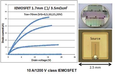
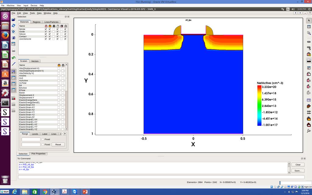
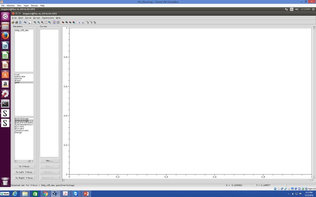
19 Simulation of power MOSFETs in Sentaurus These slides a part of Lecture 4 on the modeling of WBG semiconductor devices. Petru Andrei, Florida State University Follow the steps presented on these slides to open, mesh, and compute the I-C characteristics of a power MOSFET in Sentaurus.
20
21
22
23
24
25

26
27
28
29
30
31
32
33
34
35
Introduction to Power Semiconductor Devices
 ECE442 Power Semiconductor Devices and Integrated Circuits Introduction to Power Semiconductor Devices Zheng Yang (ERF 3017, email: yangzhen@uic.edu) Power Semiconductor Devices Applications System Ratings
Appendix 1: List of symbols
 Appendix 1: List of symbols Symbol Description MKS Units a Acceleration m/s 2 a 0 Bohr radius m A Area m 2 A* Richardson constant m/s A C Collector area m 2 A E Emitter area m 2 b Bimolecular recombination
Semiconductor Physics Problems 2015
 Semiconductor Physics Problems 2015 Page and figure numbers refer to Semiconductor Devices Physics and Technology, 3rd edition, by SM Sze and M-K Lee 1. The purest semiconductor crystals it is possible
1 Name: Student number: DEPARTMENT OF PHYSICS AND PHYSICAL OCEANOGRAPHY MEMORIAL UNIVERSITY OF NEWFOUNDLAND. Fall :00-11:00
 1 Name: DEPARTMENT OF PHYSICS AND PHYSICAL OCEANOGRAPHY MEMORIAL UNIVERSITY OF NEWFOUNDLAND Final Exam Physics 3000 December 11, 2012 Fall 2012 9:00-11:00 INSTRUCTIONS: 1. Answer all seven (7) questions.
Chapter 1 Overview of Semiconductor Materials and Physics
 Chapter 1 Overview of Semiconductor Materials and Physics Professor Paul K. Chu Conductivity / Resistivity of Insulators, Semiconductors, and Conductors Semiconductor Elements Period II III IV V VI 2 B
Institute of Solid State Physics. Technische Universität Graz. Exam. Feb 2, 10:00-11:00 P2
 Technische Universität Graz nstitute of Solid State Physics Exam Feb 2, 10:00-11:00 P2 Exam Four questions, two from the online list. Calculator is ok. No notes. Explain some concept: (tunnel contact,
Lecture 8. Equations of State, Equilibrium and Einstein Relationships and Generation/Recombination
 Lecture 8 Equations of State, Equilibrium and Einstein Relationships and Generation/Recombination Reading: (Cont d) Notes and Anderson 2 sections 3.4-3.11 Energy Equilibrium Concept Consider a non-uniformly
n N D n p = n i p N A
 Summary of electron and hole concentration in semiconductors Intrinsic semiconductor: E G n kt i = pi = N e 2 0 Donor-doped semiconductor: n N D where N D is the concentration of donor impurity Acceptor-doped
Spring Semester 2012 Final Exam
 Spring Semester 2012 Final Exam Note: Show your work, underline results, and always show units. Official exam time: 2.0 hours; an extension of at least 1.0 hour will be granted to anyone. Materials parameters
Quiz #1 Practice Problem Set
 Name: Student Number: ELEC 3908 Physical Electronics Quiz #1 Practice Problem Set? Minutes January 22, 2016 - No aids except a non-programmable calculator - All questions must be answered - All questions
Lecture 2. Introduction to semiconductors Structures and characteristics in semiconductors
 Lecture 2 Introduction to semiconductors Structures and characteristics in semiconductors Semiconductor p-n junction Metal Oxide Silicon structure Semiconductor contact Literature Glen F. Knoll, Radiation
CHAPTER 4: P-N P N JUNCTION Part 2. M.N.A. Halif & S.N. Sabki
 CHAPTER 4: P-N P N JUNCTION Part 2 Part 2 Charge Storage & Transient Behavior Junction Breakdown Heterojunction CHARGE STORAGE & TRANSIENT BEHAVIOR Once injected across the junction, the minority carriers
Chapter 7. The pn Junction
 Chapter 7 The pn Junction Chapter 7 PN Junction PN junction can be fabricated by implanting or diffusing donors into a P-type substrate such that a layer of semiconductor is converted into N type. Converting
Semiconductor Physics fall 2012 problems
 Semiconductor Physics fall 2012 problems 1. An n-type sample of silicon has a uniform density N D = 10 16 atoms cm -3 of arsenic, and a p-type silicon sample has N A = 10 15 atoms cm -3 of boron. For each
Lecture 17 - The Bipolar Junction Transistor (I) Forward Active Regime. April 10, 2003
 Forward Active Regime. April 10, 2003") 6.012 - Microelectronic Devices and Circuits - Spring 2003 Lecture 17-1 Lecture 17 - The Bipolar Junction Transistor (I) Contents: Forward Active Regime April 10, 2003 1. BJT: structure and basic operation
6.012 - Microelectronic Devices and Circuits - Spring 2003 Lecture 17-1 Lecture 17 - The Bipolar Junction Transistor (I) Contents: Forward Active Regime April 10, 2003 1. BJT: structure and basic operation
Semiconductor Junctions
 8 Semiconductor Junctions Almost all solar cells contain junctions between different materials of different doping. Since these junctions are crucial to the operation of the solar cell, we will discuss
8.1 Drift diffusion model
 8.1 Drift diffusion model Advanced theory 1 Basic Semiconductor Equations The fundamentals of semiconductor physic are well described by tools of quantum mechanic. This point of view gives us a model of
Session 6: Solid State Physics. Diode
 Session 6: Solid State Physics Diode 1 Outline A B C D E F G H I J 2 Definitions / Assumptions Homojunction: the junction is between two regions of the same material Heterojunction: the junction is between
Memories Bipolar Transistors
 Technische Universität Graz nstitute of Solid State Physics Memories Bipolar Transistors Technische Universität Graz nstitute of Solid State Physics Exams February 5 March 7 April 18 June 27 Exam Four
Metal Semiconductor Contacts
 Metal Semiconductor Contacts The investigation of rectification in metal-semiconductor contacts was first described by Braun [33-35], who discovered in 1874 the asymmetric nature of electrical conduction
Section 12: Intro to Devices
 Section 12: Intro to Devices Extensive reading materials on reserve, including Robert F. Pierret, Semiconductor Device Fundamentals EE143 Ali Javey Bond Model of Electrons and Holes Si Si Si Si Si Si Si
Electronic Devices & Circuits
 Electronic Devices & Circuits For Electronics & Communication Engineering By www.thegateacademy.com Syllabus Syllabus for Electronic Devices Energy Bands in Intrinsic and Extrinsic Silicon, Carrier Transport,
GaN based transistors
 GaN based transistors S FP FP dielectric G SiO 2 Al x Ga 1-x N barrier i-gan Buffer i-sic D Transistors "The Transistor was probably the most important invention of the 20th Century The American Institute
ELEC 3908, Physical Electronics, Lecture 18. The Early Effect, Breakdown and Self-Heating
 ELEC 3908, Physical Electronics, Lecture 18 The Early Effect, Breakdown and Self-Heating Lecture Outline Previous 2 lectures analyzed fundamental static (dc) carrier transport in the bipolar transistor
Lecture 6 PN Junction and MOS Electrostatics(III) Metal-Oxide-Semiconductor Structure
 Metal-Oxide-Semiconductor Structure") Lecture 6 PN Junction and MOS Electrostatics(III) Metal-Oxide-Semiconductor Structure Outline 1. Introduction to MOS structure 2. Electrostatics of MOS in thermal equilibrium 3. Electrostatics of MOS with
Lecture 6 PN Junction and MOS Electrostatics(III) Metal-Oxide-Semiconductor Structure Outline 1. Introduction to MOS structure 2. Electrostatics of MOS in thermal equilibrium 3. Electrostatics of MOS with
Fundamentals of Semiconductor Physics
 Fall 2007 Fundamentals of Semiconductor Physics 万 歆 Zhejiang Institute of Modern Physics xinwan@zimp.zju.edu.cn http://zimp.zju.edu.cn/~xinwan/ Transistor technology evokes new physics The objective of
MSE 310/ECE 340: Electrical Properties of Materials Fall 2014 Department of Materials Science and Engineering Boise State University
 MSE 310/ECE 340: Electrical Properties of Materials Fall 2014 Department of Materials Science and Engineering Boise State University Practice Final Exam 1 Read the questions carefully Label all figures
13. Bipolar transistors
 Technische Universität Graz Institute of Solid State Physics 13. Bipolar transistors Jan. 16, 2019 Technische Universität Graz Institute of Solid State Physics bipolar transistors npn transistor collector
Classification of Solids
 Classification of Solids Classification by conductivity, which is related to the band structure: (Filled bands are shown dark; D(E) = Density of states) Class Electron Density Density of States D(E) Examples
Section 12: Intro to Devices
 Section 12: Intro to Devices Extensive reading materials on reserve, including Robert F. Pierret, Semiconductor Device Fundamentals Bond Model of Electrons and Holes Si Si Si Si Si Si Si Si Si Silicon
Semiconductor device structures are traditionally divided into homojunction devices
 0. Introduction: Semiconductor device structures are traditionally divided into homojunction devices (devices consisting of only one type of semiconductor material) and heterojunction devices (consisting
Consider a uniformly doped PN junction, in which one region of the semiconductor is uniformly doped with acceptor atoms and the adjacent region is
 CHAPTER 7 The PN Junction Consider a uniformly doped PN junction, in which one region of the semiconductor is uniformly doped with acceptor atoms and the adjacent region is uniformly doped with donor atoms.
Semiconductor Module
 Semiconductor Module Optics Seminar July 18, 2018 Yosuke Mizuyama, Ph.D. COMSOL, Inc. The COMSOL Product Suite Governing Equations Semiconductor Schrödinger Equation Semiconductor Optoelectronics, FD Semiconductor
Course overview. Me: Dr Luke Wilson. The course: Physics and applications of semiconductors. Office: E17 open door policy
 Course overview Me: Dr Luke Wilson Office: E17 open door policy email: luke.wilson@sheffield.ac.uk The course: Physics and applications of semiconductors 10 lectures aim is to allow time for at least one
R. Ludwig and G. Bogdanov RF Circuit Design: Theory and Applications 2 nd edition. Figures for Chapter 6
 R. Ludwig and G. Bogdanov RF Circuit Design: Theory and Applications 2 nd edition Figures for Chapter 6 Free electron Conduction band Hole W g W C Forbidden Band or Bandgap W V Electron energy Hole Valence
Lecture 2. Introduction to semiconductors Structures and characteristics in semiconductors
 Lecture 2 Introduction to semiconductors Structures and characteristics in semiconductors Semiconductor p-n junction Metal Oxide Silicon structure Semiconductor contact Literature Glen F. Knoll, Radiation
Final Examination EE 130 December 16, 1997 Time allotted: 180 minutes
 Final Examination EE 130 December 16, 1997 Time allotted: 180 minutes Problem 1: Semiconductor Fundamentals [30 points] A uniformly doped silicon sample of length 100µm and cross-sectional area 100µm 2
MOS CAPACITOR AND MOSFET
 EE336 Semiconductor Devices 1 MOS CAPACITOR AND MOSFET Dr. Mohammed M. Farag Ideal MOS Capacitor Semiconductor Devices Physics and Technology Chapter 5 EE336 Semiconductor Devices 2 MOS Capacitor Structure
EECS130 Integrated Circuit Devices
 EECS130 Integrated Circuit Devices Professor Ali Javey 8/30/2007 Semiconductor Fundamentals Lecture 2 Read: Chapters 1 and 2 Last Lecture: Energy Band Diagram Conduction band E c E g Band gap E v Valence
ECE 305 Fall Final Exam (Exam 5) Wednesday, December 13, 2017
 Wednesday, December 13, 2017") NAME: PUID: ECE 305 Fall 017 Final Exam (Exam 5) Wednesday, December 13, 017 This is a closed book exam. You may use a calculator and the formula sheet at the end of this exam. Following the ECE policy,
NAME: PUID: ECE 305 Fall 017 Final Exam (Exam 5) Wednesday, December 13, 017 This is a closed book exam. You may use a calculator and the formula sheet at the end of this exam. Following the ECE policy,
Schottky Rectifiers Zheng Yang (ERF 3017,
 ECE442 Power Semiconductor Devices and Integrated Circuits Schottky Rectifiers Zheng Yang (ERF 3017, email: yangzhen@uic.edu) Power Schottky Rectifier Structure 2 Metal-Semiconductor Contact The work function
Solid State Physics SEMICONDUCTORS - IV. Lecture 25. A.H. Harker. Physics and Astronomy UCL
 Solid State Physics SEMICONDUCTORS - IV Lecture 25 A.H. Harker Physics and Astronomy UCL 9.9 Carrier diffusion and recombination Suppose we have a p-type semiconductor, i.e. n h >> n e. (1) Create a local
EE 6313 Homework Assignments
 EE 6313 Homework Assignments 1. Homework I: Chapter 1: 1.2, 1.5, 1.7, 1.10, 1.12 [Lattice constant only] (Due Sept. 1, 2009). 2. Homework II: Chapter 1, 2: 1.17, 2.1 (a, c) (k = π/a at zone edge), 2.3
EE 3329 Electronic Devices Syllabus ( Extended Play )
") EE 3329 - Electronic Devices Syllabus EE 3329 Electronic Devices Syllabus ( Extended Play ) The University of Texas at El Paso The following concepts can be part of the syllabus for the Electronic Devices
EE 3329 - Electronic Devices Syllabus EE 3329 Electronic Devices Syllabus ( Extended Play ) The University of Texas at El Paso The following concepts can be part of the syllabus for the Electronic Devices
Theory of Electrical Characterization of Semiconductors
 Theory of Electrical Characterization of Semiconductors P. Stallinga Universidade do Algarve U.C.E.H. A.D.E.E.C. OptoElectronics SELOA Summer School May 2000, Bologna (It) Overview Devices: bulk Schottky
ELECTRONIC DEVICES AND CIRCUITS SUMMARY
 ELECTRONIC DEVICES AND CIRCUITS SUMMARY Classification of Materials: Insulator: An insulator is a material that offers a very low level (or negligible) of conductivity when voltage is applied. Eg: Paper,
Lecture 04 Review of MOSFET
 ECE 541/ME 541 Microelectronic Fabrication Techniques Lecture 04 Review of MOSFET Zheng Yang (ERF 3017, email: yangzhen@uic.edu) What is a Transistor? A Switch! An MOS Transistor V GS V T V GS S Ron D
Lecture 5 Junction characterisation
 Lecture 5 Junction characterisation Jon Major October 2018 The PV research cycle Make cells Measure cells Despair Repeat 40 1.1% 4.9% Data Current density (ma/cm 2 ) 20 0-20 -1.0-0.5 0.0 0.5 1.0 Voltage
Semiconductors. SEM and EDAX images of an integrated circuit. SEM EDAX: Si EDAX: Al. Institut für Werkstoffe der ElektrotechnikIWE
 SEM and EDAX images of an integrated circuit SEM EDAX: Si EDAX: Al source: [Cal 99 / 605] M&D-.PPT, slide: 1, 12.02.02 Classification semiconductors electronic semiconductors mixed conductors ionic conductors
KATIHAL FİZİĞİ MNT-510
 KATIHAL FİZİĞİ MNT-510 YARIİLETKENLER Kaynaklar: Katıhal Fiziği, Prof. Dr. Mustafa Dikici, Seçkin Yayıncılık Katıhal Fiziği, Şakir Aydoğan, Nobel Yayıncılık, Physics for Computer Science Students: With
EE301 Electronics I , Fall
 EE301 Electronics I 2018-2019, Fall 1. Introduction to Microelectronics (1 Week/3 Hrs.) Introduction, Historical Background, Basic Consepts 2. Rewiev of Semiconductors (1 Week/3 Hrs.) Semiconductor materials
Solid State Electronics. Final Examination
 The University of Toledo EECS:4400/5400/7400 Solid State Electronic Section elssf08fs.fm - 1 Solid State Electronics Final Examination Problems Points 1. 1. 14 3. 14 Total 40 Was the exam fair? yes no
smal band gap Saturday, April 9, 2011
 small band gap upper (conduction) band empty small gap valence band filled 2s 2p 2s 2p hybrid (s+p)band 2p no gap 2s (depend on the crystallographic orientation) extrinsic semiconductor semi-metal electron
Schottky diodes. JFETs - MESFETs - MODFETs
 Technische Universität Graz Institute of Solid State Physics Schottky diodes JFETs - MESFETs - MODFETs Quasi Fermi level When the charge carriers are not in equilibrium the Fermi energy can be different
Diodes. anode. cathode. cut-off. Can be approximated by a piecewise-linear-like characteristic. Lecture 9-1
 Diodes mplest nonlinear circuit element Basic operation sets the foundation for Bipolar Junction Transistors (BJTs) Also present in Field Effect Transistors (FETs) Ideal diode characteristic anode cathode
PHYSICAL ELECTRONICS(ECE3540) CHAPTER 9 METAL SEMICONDUCTOR AND SEMICONDUCTOR HETERO-JUNCTIONS
 CHAPTER 9 METAL SEMICONDUCTOR AND SEMICONDUCTOR HETERO-JUNCTIONS") PHYSICAL ELECTRONICS(ECE3540) CHAPTER 9 METAL SEMICONDUCTOR AND SEMICONDUCTOR HETERO-JUNCTIONS Tennessee Technological University Monday, November 11, 013 1 Introduction Chapter 4: we considered the semiconductor
PHYSICAL ELECTRONICS(ECE3540) CHAPTER 9 METAL SEMICONDUCTOR AND SEMICONDUCTOR HETERO-JUNCTIONS Tennessee Technological University Monday, November 11, 013 1 Introduction Chapter 4: we considered the semiconductor
This is the 15th lecture of this course in which we begin a new topic, Excess Carriers. This topic will be covered in two lectures.
 Solid State Devices Dr. S. Karmalkar Department of Electronics and Communication Engineering Indian Institute of Technology, Madras Lecture - 15 Excess Carriers This is the 15th lecture of this course
Student Number: CARLETON UNIVERSITY SELECTED FINAL EXAMINATION QUESTIONS
 Name: CARLETON UNIVERSITY SELECTE FINAL EXAMINATION QUESTIONS URATION: 6 HOURS epartment Name & Course Number: ELEC 3908 Course Instructors: S. P. McGarry Authorized Memoranda: Non-programmable calculators
Introduction to Optoelectronic Device Simulation by Joachim Piprek
 NUSOD 5 Tutorial MA Introduction to Optoelectronic Device Simulation by Joachim Piprek Outline:. Introduction: VCSEL Example. Electron Energy Bands 3. Drift-Diffusion Model 4. Thermal Model 5. Gain/Absorption
ECE-305: Spring 2018 Final Exam Review
 C-305: Spring 2018 Final xam Review Pierret, Semiconductor Device Fundamentals (SDF) Chapters 10 and 11 (pp. 371-385, 389-403) Professor Peter Bermel lectrical and Computer ngineering Purdue University,
8. Schottky contacts / JFETs
 Technische Universität Graz Institute of Solid State Physics 8. Schottky contacts / JFETs Nov. 21, 2018 Technische Universität Graz Institute of Solid State Physics metal - semiconductor contacts Photoelectric
The Electromagnetic Properties of Materials
 The lectromagnetic Properties of Materials lectrical conduction Metals Semiconductors Insulators (dielectrics) Superconductors Magnetic materials Ferromagnetic materials Others Photonic Materials (optical)
ECE 497 JS Lecture - 12 Device Technologies
 ECE 497 JS Lecture - 12 Device Technologies Spring 2004 Jose E. Schutt-Aine Electrical & Computer Engineering University of Illinois jose@emlab.uiuc.edu 1 NMOS Transistor 2 ρ Source channel charge density
Engineering 2000 Chapter 8 Semiconductors. ENG2000: R.I. Hornsey Semi: 1
 Engineering 2000 Chapter 8 Semiconductors ENG2000: R.I. Hornsey Semi: 1 Overview We need to know the electrical properties of Si To do this, we must also draw on some of the physical properties and we
ECE-305: Spring 2018 Exam 2 Review
 ECE-305: Spring 018 Exam Review Pierret, Semiconductor Device Fundamentals (SDF) Chapter 3 (pp. 75-138) Chapter 5 (pp. 195-6) Professor Peter Bermel Electrical and Computer Engineering Purdue University,
EECS130 Integrated Circuit Devices
 EECS130 Integrated Circuit Devices Professor Ali Javey 9/18/2007 P Junctions Lecture 1 Reading: Chapter 5 Announcements For THIS WEEK OLY, Prof. Javey's office hours will be held on Tuesday, Sept 18 3:30-4:30
EECS143 Microfabrication Technology
 EECS143 Microfabrication Technology Professor Ali Javey Introduction to Materials Lecture 1 Evolution of Devices Yesterday s Transistor (1947) Today s Transistor (2006) Why Semiconductors? Conductors e.g
For the following statements, mark ( ) for true statement and (X) for wrong statement and correct it.
 for true statement and (X) for wrong statement and correct it.") Benha University Faculty of Engineering Shoubra Electrical Engineering Department First Year communications. Answer all the following questions Illustrate your answers with sketches when necessary. The
Benha University Faculty of Engineering Shoubra Electrical Engineering Department First Year communications. Answer all the following questions Illustrate your answers with sketches when necessary. The
Semiconductor Physical Electronics
 Semiconductor Physical Electronics Sheng S. Li Department of Electrical Engineering University of Florida Gainesville, Florida Plenum Press New York and London Contents CHAPTER 1. Classification of Solids
ET3034TUx Utilization of band gap energy
 ET3034TUx - 3.3.1 - Utilization of band gap energy In the last two weeks we have discussed the working principle of a solar cell and the external parameters that define the performance of a solar cell.
3.1 Introduction to Semiconductors. Y. Baghzouz ECE Department UNLV
 3.1 Introduction to Semiconductors Y. Baghzouz ECE Department UNLV Introduction In this lecture, we will cover the basic aspects of semiconductor materials, and the physical mechanisms which are at the
ELEC 4700 Assignment #2
 ELEC 4700 Assignment #2 Question 1 (Kasop 4.2) Molecular Orbitals and Atomic Orbitals Consider a linear chain of four identical atoms representing a hypothetical molecule. Suppose that each atomic wavefunction
12. Memories / Bipolar transistors
 Technische Universität Graz Institute of Solid State Physics 12. Memories / Bipolar transistors Jan. 9, 2019 Technische Universität Graz Institute of Solid State Physics Exams January 31 March 8 May 17
Schottky Diodes (M-S Contacts)
") Schottky Diodes (M-S Contacts) Three MITs of the Day Band diagrams for ohmic and rectifying Schottky contacts Similarity to and difference from bipolar junctions on electrostatic and IV characteristics.
Schottky Diodes (M-S Contacts) Three MITs of the Day Band diagrams for ohmic and rectifying Schottky contacts Similarity to and difference from bipolar junctions on electrostatic and IV characteristics.
Electron Energy, E E = 0. Free electron. 3s Band 2p Band Overlapping energy bands. 3p 3s 2p 2s. 2s Band. Electrons. 1s ATOM SOLID.
 Electron Energy, E Free electron Vacuum level 3p 3s 2p 2s 2s Band 3s Band 2p Band Overlapping energy bands Electrons E = 0 1s ATOM 1s SOLID In a metal the various energy bands overlap to give a single
Peak Electric Field. Junction breakdown occurs when the peak electric field in the PN junction reaches a critical value. For the N + P junction,
 Peak Electric Field Junction breakdown occurs when the peak electric field in the P junction reaches a critical value. For the + P junction, qa E ( x) ( xp x), s W dep 2 s ( bi Vr ) 2 s potential barrier
Current mechanisms Exam January 27, 2012
 Current mechanisms Exam January 27, 2012 There are four mechanisms that typically cause currents to flow: thermionic emission, diffusion, drift, and tunneling. Explain briefly which kind of current mechanisms
FYS 3028/8028 Solar Energy and Energy Storage. Calculator with empty memory Language dictionaries
 Faculty of Science and Technology Exam in: FYS 3028/8028 Solar Energy and Energy Storage Date: 11.05.2016 Time: 9-13 Place: Åsgårdvegen 9 Approved aids: Type of sheets (sqares/lines): Number of pages incl.
Electrical Characteristics of MOS Devices
 Electrical Characteristics of MOS Devices The MOS Capacitor Voltage components Accumulation, Depletion, Inversion Modes Effect of channel bias and substrate bias Effect of gate oide charges Threshold-voltage
Sheng S. Li. Semiconductor Physical Electronics. Second Edition. With 230 Figures. 4) Springer
 Springer") Sheng S. Li Semiconductor Physical Electronics Second Edition With 230 Figures 4) Springer Contents Preface 1. Classification of Solids and Crystal Structure 1 1.1 Introduction 1 1.2 The Bravais Lattice
Sheng S. Li Semiconductor Physical Electronics Second Edition With 230 Figures 4) Springer Contents Preface 1. Classification of Solids and Crystal Structure 1 1.1 Introduction 1 1.2 The Bravais Lattice
Electronic Circuits 1. Transistor Devices. Contents BJT and FET Characteristics Operations. Prof. C.K. Tse: Transistor devices
 Electronic Circuits 1 Transistor Devices Contents BJT and FET Characteristics Operations 1 What is a transistor? Three-terminal device whose voltage-current relationship is controlled by a third voltage
EE 446/646 Photovoltaic Devices I. Y. Baghzouz
 EE 446/646 Photovoltaic Devices I Y. Baghzouz What is Photovoltaics? First used in about 1890, the word has two parts: photo, derived from the Greek word for light, volt, relating to electricity pioneer
OPTI510R: Photonics. Khanh Kieu College of Optical Sciences, University of Arizona Meinel building R.626
 OPTI510R: Photonics Khanh Kieu College of Optical Sciences, University of Arizona kkieu@optics.arizona.edu Meinel building R.626 Announcements Homework #6 is assigned, due May 1 st Final exam May 8, 10:30-12:30pm
Digital Integrated CircuitDesign
 Digital Integrated CircuitDesign Lecture 5a Bipolar Transistor Dep. Region Neutral Base n(0) b B C n b0 P C0 P e0 P C xn 0 xp 0 x n(w) b W B Adib Abrishamifar EE Department IUST Contents Bipolar Transistor
EE105 Fall 2015 Microelectronic Devices and Circuits: Semiconductor Fabrication and PN Junctions
 EE105 Fall 2015 Microelectronic Devices and Circuits: Semiconductor Fabrication and PN Junctions Prof. Ming C. Wu wu@eecs.berkeley.edu 511 Sutardja Dai Hall (SDH) 1 pn Junction p-type semiconductor in
Recitation 17: BJT-Basic Operation in FAR
 Recitation 17: BJT-Basic Operation in FAR BJT stands for Bipolar Junction Transistor 1. Can be thought of as two p-n junctions back to back, you can have pnp or npn. In analogy to MOSFET small current
Lecture 4 - PN Junction and MOS Electrostatics (I) Semiconductor Electrostatics in Thermal Equilibrium September 20, 2005
 Semiconductor Electrostatics in Thermal Equilibrium September 20, 2005") 6.012 - Microelectronic Devices and Circuits - Fall 2005 Lecture 4-1 Contents: Lecture 4 - PN Junction and MOS Electrostatics (I) Semiconductor Electrostatics in Thermal Equilibrium September 20, 2005
6.012 - Microelectronic Devices and Circuits - Fall 2005 Lecture 4-1 Contents: Lecture 4 - PN Junction and MOS Electrostatics (I) Semiconductor Electrostatics in Thermal Equilibrium September 20, 2005
Semiconductor Detectors are Ionization Chambers. Detection volume with electric field Energy deposited positive and negative charge pairs
 1 V. Semiconductor Detectors V.1. Principles Semiconductor Detectors are Ionization Chambers Detection volume with electric field Energy deposited positive and negative charge pairs Charges move in field
Devices. chapter Introduction. 1.2 Silicon Conductivity
 chapter 1 Devices 1.1 Introduction The properties and performance of analog bicmos integrated circuits are dependent on the devices used to construct them. This chapter is a review of the operation of
Lecture 2. Introduction to semiconductors Structures and characteristics in semiconductors. Fabrication of semiconductor sensor
 Lecture 2 Introduction to semiconductors Structures and characteristics in semiconductors Semiconductor p-n junction Metal Oxide Silicon structure Semiconductor contact Fabrication of semiconductor sensor
Lecture 15 OUTLINE. MOSFET structure & operation (qualitative) Review of electrostatics The (N)MOS capacitor
 Review of electrostatics The (N)MOS capacitor") Lecture 15 OUTLINE MOSFET structure & operation (qualitative) Review of electrostatics The (N)MOS capacitor Electrostatics Charge vs. voltage characteristic Reading: Chapter 6.1 6.2.1 EE15 Spring 28 Lecture
Lecture 15 OUTLINE MOSFET structure & operation (qualitative) Review of electrostatics The (N)MOS capacitor Electrostatics Charge vs. voltage characteristic Reading: Chapter 6.1 6.2.1 EE15 Spring 28 Lecture
FIELD-EFFECT TRANSISTORS
 FIEL-EFFECT TRANSISTORS 1 Semiconductor review 2 The MOS capacitor 2 The enhancement-type N-MOS transistor 3 I-V characteristics of enhancement MOSFETS 4 The output characteristic of the MOSFET in saturation
Lecture 15 OUTLINE. MOSFET structure & operation (qualitative) Review of electrostatics The (N)MOS capacitor
 Review of electrostatics The (N)MOS capacitor") Lecture 15 OUTLINE MOSFET structure & operation (qualitative) Review of electrostatics The (N)MOS capacitor Electrostatics t ti Charge vs. voltage characteristic Reading: Chapter 6.1 6.2.1 EE105 Fall 2007
Lecture 15 OUTLINE MOSFET structure & operation (qualitative) Review of electrostatics The (N)MOS capacitor Electrostatics t ti Charge vs. voltage characteristic Reading: Chapter 6.1 6.2.1 EE105 Fall 2007
1 cover it in more detail right away, 2 indicate when it will be covered in detail, or. 3 invite you to office hours.
 14 1 8 6 IBM ES9 Bipolar Fujitsu VP IBM 39S Pulsar 4 IBM 39 IBM RY6 CDC Cyber 5 IBM 4381 IBM RY4 IBM 381 Apache Fujitsu M38 IBM 37 Merced IBM 36 IBM 333 Vacuum Pentium II(DSIP) 195 196 197 198 199 NTT
Lecture 7 - PN Junction and MOS Electrostatics (IV) Electrostatics of Metal-Oxide-Semiconductor Structure. September 29, 2005
 Electrostatics of Metal-Oxide-Semiconductor Structure. September 29, 2005") 6.12 - Microelectronic Devices and Circuits - Fall 25 Lecture 7-1 Lecture 7 - PN Junction and MOS Electrostatics (IV) Electrostatics of Metal-Oide-Semiconductor Structure September 29, 25 Contents: 1.
6.12 - Microelectronic Devices and Circuits - Fall 25 Lecture 7-1 Lecture 7 - PN Junction and MOS Electrostatics (IV) Electrostatics of Metal-Oide-Semiconductor Structure September 29, 25 Contents: 1.
Uniform excitation: applied field and optical generation. Non-uniform doping/excitation: diffusion, continuity
 6.012 - Electronic Devices and Circuits Lecture 2 - Uniform Excitation; Non-uniform conditions Announcements Review Carrier concentrations in TE given the doping level What happens above and below room
Semiconductor Fundamentals. Professor Chee Hing Tan
 Semiconductor Fundamentals Professor Chee Hing Tan c.h.tan@sheffield.ac.uk Why use semiconductor? Microprocessor Transistors are used in logic circuits that are compact, low power consumption and affordable.
Lecture 7 PN Junction and MOS Electrostatics(IV) Metal Oxide Semiconductor Structure (contd.)
 Metal Oxide Semiconductor Structure (contd.)") Lecture 7 PN Junction and MOS Electrostatics(IV) Metal Oxide Semiconductor Structure (contd.) Outline 1. Overview of MOS electrostatics under bias 2. Depletion regime 3. Flatband 4. Accumulation regime
Lecture 7 PN Junction and MOS Electrostatics(IV) Metal Oxide Semiconductor Structure (contd.) Outline 1. Overview of MOS electrostatics under bias 2. Depletion regime 3. Flatband 4. Accumulation regime
EE105 - Fall 2006 Microelectronic Devices and Circuits
 EE105 - Fall 2006 Microelectronic Devices and Circuits Prof. Jan M. Rabaey (jan@eecs) Lecture 21: Bipolar Junction Transistor Administrative Midterm Th 6:30-8pm in Sibley Auditorium Covering everything
A. OTHER JUNCTIONS B. SEMICONDUCTOR HETEROJUNCTIONS -- MOLECULES AT INTERFACES: ORGANIC PHOTOVOLTAIC BULK HETEROJUNCTION DYE-SENSITIZED SOLAR CELL
 A. OTHER JUNCTIONS B. SEMICONDUCTOR HETEROJUNCTIONS -- MOLECULES AT INTERFACES: ORGANIC PHOTOVOLTAIC BULK HETEROJUNCTION DYE-SENSITIZED SOLAR CELL February 9 and 14, 2012 The University of Toledo, Department