Chapter 13 Bipolar Junction Transistors
|
|
|
- Christine Williamson
- 6 years ago
- Views:
Transcription
1 Chapter 3 ipolar Junction Transistors
2 Goal. ipolar Junction Transistor Operation in amplifier circuits. 2. Load-line Analysis & Nonlinear Distortion. 3. Large-signal equialent circuits to analyze JT circuits. 4. ias circuits. 5. Small-signal equialent circuits to analyze JT amplifiers. 6. Seeral Important Amplifier Configurations.


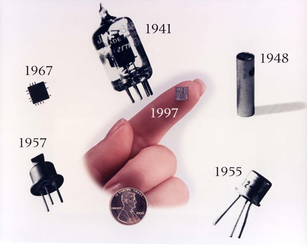
3 st Transistor rattain and ardeen's pnp point-contact germanium transistor operated s a speech amplifier with a power gain of 8 on December 23, 947
4 Explanation of st Transistor his picture shows the workbench of John ardeen and Walter rattain t ell Laboratories. They were supposed to be doing fundamental esearch about crystal surfaces. The experimental results hadn't been ery good, though, and there's a rumor that their boss, William hockley, came near to canceling the project. ut in 947, working lone, they switched to using tremendously pure materials. It dawned n them that they could build the circuit in the picture. It was a working mplifier! John and Walter submitted a patent for the first working oint contact transistor. Shockley was furious and took their work and nented the junction transistor and submitted a patent for it 9 days ater. The three shared a Nobel Prize. ardeen and rattain continued in esearch (and ardeen later won another Nobel). Shockley quit to start emiconductor company in Palo Alto. It folded, but its staff went on to nent the integrated circuit (the "chip") and to found Intel Corporation y 960, all important computers used transistors for logic, and ferrite
5 - from ell Laboratories ecord magazine January 975, p.74 Major Milestones in Transistor Electronics POINT CONTACT TANSISTO SINGLE-CYSTAL GEMANIUM 95 - GOWN JUNCTION TANSISTO ALLOY JUNCTION TANSISTO ZONE MELTING AND EFINING SINGLE-CYSTAL SILICON DIFFUSED -ASE TANSISTOS OXIDE MASKING PLANA TANSISTO MOS TANSISTO EPITAXIAL TANSISTO 96 - INTEGATED CICUITS

6 Close-Up of 2N23 transistor by Western Electric in 954
7
8 Transistor 948 년미국 ell Lab 의 Walter Houser rattain, John ardeen 및 William radford Shockley 는반도체격자구조의시편 ( 試片 ) 에가는도체선을접촉시켜주면전기신호의증폭작용을나타내는것을발견하여이를트랜지스터라고명명하였다. 이것이그동안신호증폭의구실을해오던진공관 ( 眞空管 ) 과대치되는트랜지스터의시초가된것이다. 트랜지스터그자체가소형이어서이를사용하는기기 ( 機器 ) 는진공관을사용할때에비하여소형이되며, 가볍고소비전력이적어편리하다. 초기에는잡음 주파수특성이나쁘고, 증폭도도충분하지못하였으나, 그후많이개량되어아주대전력을다룰수있는등특수한경우를제외하고는진공관에대치되었다. - 두산백과사전 - The Most asic & Important Actie Component - Power Amplification - IC uses more recently : interfacing required - if no proper IC, only transistor can do something.
9 Transistor Function: Current Amplification Type : PNP, NPN Type Code : PNP High Frequency (2SA ) PNP Low Frequency (2S ) NPN High Frequency (2SC ) NPN Low Frequency (2SD ) 마이너스전압측을접지로, 플러스전압측을전원으로하는회로의경우, NPN 타입쪽이사용하기쉽다.


10 Lead in Transistor NPN : 2SC85 NPN : 2SD880 품명이인쇄되어있는면을바라보았을때, 오른쪽리드가베이스중앙의리드가컬렉터왼쪽의리드가이미터 품명이인쇄되어있는면을바라보았을때, 오른쪽리드가이미터중앙의리드가컬렉터왼쪽의리드가베이스 지스터의종류에따라리드의내용이다르기때문에매뉴얼등을참조하여확인할필요가있다 같은 npn 인데리드가다름
11 Transistor Man Transistor Man obseres the base current and adjusts the output rheostat in an attempt to maintain the output current h FE times larger
12 asic Transistor Model In npn Transistor, for example. Collector must be more positie than Emitter 2. ase-emitter and ase-collector behae like diode 3. Maximum Parameter V CE : Voltage between Collector and Emitter at open ase V E : Voltage between ase and Emitter I C : Collector Current I : ase Current P : Power Dissipation at Collector at C 25o C f T : frequency at I C I 4. Collector Current is proportional to ase Current I C h FE I h FE : Current Gain 00 ~ 300 Note : h FE is not a good parameter {range : } Circuit based on a particular h FE alue is a bad circuit

 Typical")
13 Schematic of JT Transistor Small fraction of Emitter Current flows into ase (C- junction : eerse ias, -E Junction : Forward ias) Typical Junction Connection
14 Equations of Operation t -E Junction Schokley Equation KCL i E E I ES exp VT i i + E C i et α i i C E i C I s E i C αi ES exp VT exp V E T β i i C I α α s αi ES : Scale Current : Typically 00 i β i C
15 Common-Emitter Characteristics P N N C C < 0 with E < CE E CE -C junction : eerse ias, -E Junction : Forward ias
16 Input Output < 0 with < C E CE E must be larger than 0.6 ~ 0.7V i βi 00i C
17 Analysis of Common-Emitter Amplifier AC VL in Circuits Input () t i ( t) ( t) + DC Output + in E V CC C i C + CE
18 Load-Line Analysis of Input ( t) i ( t) ( t) V + + in E 0 E in 0 : Q point AC swing around Q Point Max i Min i i 0 Min in ( t), ( in t), i / DC AC ias Max in
19 V i + CC Load-Line Analysis of Output C C CE Max i From Input Analysis i can be Selected i β i C Min i Min CE Max CE Positie Negatie CE : Inerting Amplifier
20 in ( t) 0.4sin(2000πt) 2kΩ 40kΩ 0V 40µA.6V Q point : only DC component. 6V.6V i µ 40 5µ A i 35µ A A
21 5µ A i 35µ A IN :.2 ~ 2.0V CE : 7 ~ 3 V A 7/.2 5
22 Nonlinear Distortion in () t 0.4sin(2000πt) Output Signal is not Exactly Sine Cure in () t.2sin(2000πt) Clipping Occur : Cutoff

23 PNP ipolar Junction Transistors Except for reersal of current directions and oltage polarities, pnp JT is almost identical to the npn JT. i i i + i i E E C E I ES exp VT β C i
24 Very Typical Transistor Connection Common-Emitter Amplifier
25 Operating egion of Transistors When i C becomes zero, we say that the transistor is cutoff. When CE 0.2 V, we say that the transistor is in saturation.
26 Large-Signal DC Circuit DC ias CC C Actie egion Saturation Cut-off CC
27 Large-Signal DC Circuit Model Cutoff-egion Saturation-egion Actie-egion T : Open Circuit T : Constant Voltage Source of -0.2V Collector Voltage T : Dependant Current Sourc with ase Voltage 0.7V
28 Input Output CC C Cut-off Saturation Actie CC
29 5V Analysis of Fixed ase ias Circuit 200kΩ C kω V CC 5V 0kΩ kω i CC 0.7 CC A ic 4. 8mA µ C I β 00 : i > 0 & i C > βi Actie egion ic β i µ A 7. 5mA VCE VCC C IC 7. 85V
30 5V 00kΩ I kω β 300 i CC 0.7 CC A ic 4. 8mA C µ i > 0 & i C < βi Saturation egion ic β i µ A 2. 45mA V CE 0. 2V
31 2kΩ 5V 5V 2kΩ I V + V E E ( β + ) E V 0.7 I E 2. 5mA E i i + i i β i E C C I + + CC β C C I (µa) CE I C (ma) I E E V CE (V)
32 Analysis of Four-esistor ias Circuit Théenin Equialent : V VCC + Two esistor connected to ase Set,,i 2 2
33 KVL around -E Loop V I + V + E KCL around C--E Node I ( β +) E I E I E E 0.7V I V + KVL around C-E Loop V E ( β + ) E I βi C V CE V CC C I C E I E
34 Example of Four-esistor ias Circuit I C E 0.7V β 00 I CC 5V 3. Ω + 33k I 2 2 V VCC 5V + V VE 4.2 A IC βi 4. 2mA + µ ( ) β + E VCE VCC C IC EI E 6. 72V 2
35 Typical JT Circuit (AC Coupled) Q point is set by ias Circuit with, o Describe JT with Characteristic Model. Variation around Q point is smaller than that of Q point itself Small Signal Circuit Model is equired. i C is dependant on i or E as Described in aboe Figure Dependant Current Source Model can be used i swings around Q point E swings around Q poin


36 Small Signal Model for JT No Passie Element along Emitter Hybrid-π Model ase : esistor r π ollector : Voltage Controlled Current Source ase : esistor r π Collector : Current Controlled Current Source


37 No Element along ase T Model ase : esistor r e ollector : Voltage Controlled Current Source ase : esistor r e Collector : Current Controlled Current Source
38 Small-Signal Equialent Circuit i ( t) i i ( t) + Q i b (t) : Signal current flowing into ase I Q : DC current that flows with Zero Signa i (t) : Total ase current. ( t) V ( t) b + E EQ be I Q b (t) : Signal current flowing into ase EQ : DC current that flows with Zero Si E (t) : Total ase current. EQ
39 i I I I E ( α) I exp ES VT Q Q Q EQ + be( t) + i () t ( α) I ES exp VT EQ ( α) I ES exp VT + i Define be( t) () + be( t) t I Q exp I Q VT VT V T i π () t I Q r r π βv I T i From Preious Definition of Q point C i be r π () t I i ( t) Q + ( t) ( t) βi ( t) b b
 βi ( t) π I C b CQ")
40 Small-Signal Equialent Circuit for the JT V T i ( t) βi ( t) π I C b CQ r β
41 Typical JT Amplification Mode C E Output Terminal Choice. Common Emitter 2. Emitter Follower (Common Collector 3. Common ase
42 Common-Emitter Amplifier C, C 2 : Coupling Capacitor without Affecting DC bias from Input & Output (High Pass Filt AC signal only Pass C E : ypass Capacitor Low Impedance path for AC I E to Ground (Same as C,C 2 ) for Midband Frequency mall Signal Equialent Circuit
43 C : Coupling Capacitor without Affecting DC bias from Input (High Pass Filter) : AC signal only Pass, 2 : See Four esistor ias Parallel to ase - Emitter V V CC + 2 2

44 C 2,C E : Coupling Capacitor without Affecting DC bias from Input (High Pass Filter) : AC only Pass C E : Short Circuit to Ground C, L : See Four esistor ias Parallel to Collector - Emitter ' Total C L + C npn Transistor Hybrid π Model L
45 Small-Signal ac Equialent Circuit C L C L L π β r A L o in π β r A C o o in i b r π be in b L i β ' o Open Circuit : L 0
46 Input Impedance & Gains Z in i in in + r π A i i i / o o in in / Z L in A Z in L G A i A

47 Output Impedance Using Thenin Equialent Circuit without Load Zeroing Voltage Source Z o C
48 Common-Emitter Amplifier C, C 2 : Coupling Capacitor C E : ypass Capacitor r π βv I T CQ 2 L L C A A o Lβ r π C β Z A in i A Z + in r π G A i A Z o C
49 in.0sin( ωt) mv r π A A o βvt 63Ω ICQ Lβ 06 rπ C β 58 r π in in s s 3. 33kΩ Z A in i Ω + 53 A 2 r π Zin 28. L 667Ω G Z L L A A i Z A sin( ωt mv o in s ) C kω o C 2980
50 Source Output
51 Wae form in Common-Emitter Amp

52 Emitter Followers C, C 2 : Coupling Capacitor
53 2 + 2 L L E L + E

54 Een though the oltage gain of the emitter follower is less than unity, the current gain and power gain can be large. A r ( + β ) L + ( + β ) L π Z i + Z it Z A it i A Z i L in Z it r + β π i b G A i A ( + ) L
55 Output Impedance s s Z o i x x ( + β ) ( s + rπ ) + E
56
57 Parallel Connection Darlington Configuration
CHAPTER 13. Solutions for Exercises
 HPT 3 Solutions for xercises 3. The emitter current is gien by the Shockley equation: i S exp VT For operation with i, we hae exp >> S >>, and we can write VT i S exp VT Soling for, we hae 3.2 i 2 0 26ln
Bipolar Junction Transistor (BJT) - Introduction
 - Introduction") Bipolar Junction Transistor (BJT) - Introduction It was found in 1948 at the Bell Telephone Laboratories. It is a three terminal device and has three semiconductor regions. It can be used in signal amplification
Bipolar Junction Transistor (BJT) - Introduction It was found in 1948 at the Bell Telephone Laboratories. It is a three terminal device and has three semiconductor regions. It can be used in signal amplification
Figure 1 Basic epitaxial planar structure of NPN. Figure 2 The 3 regions of NPN (left) and PNP (right) type of transistors
 and PNP (right) type of transistors") Figure 1 Basic epitaxial planar structure of NPN Figure 2 The 3 regions of NPN (left) and PNP (right) type of transistors Lecture Notes: 2304154 Physics and Electronics Lecture 6 (2 nd Half), Year: 2007
Figure 1 Basic epitaxial planar structure of NPN Figure 2 The 3 regions of NPN (left) and PNP (right) type of transistors Lecture Notes: 2304154 Physics and Electronics Lecture 6 (2 nd Half), Year: 2007
Chapter 10 Instructor Notes
 G. izzoni, Principles and Applications of lectrical ngineering Problem solutions, hapter 10 hapter 10 nstructor Notes hapter 10 introduces bipolar junction transistors. The material on transistors has
CHAPTER.4: Transistor at low frequencies
 CHAPTER.4: Transistor at low frequencies Introduction Amplification in the AC domain BJT transistor modeling The re Transistor Model The Hybrid equivalent Model Introduction There are three models commonly
Chapter 9 Bipolar Junction Transistor
 hapter 9 ipolar Junction Transistor hapter 9 - JT ipolar Junction Transistor JT haracteristics NPN, PNP JT D iasing ollector haracteristic and Load Line ipolar Junction Transistor (JT) JT is a three-terminal
DEPARTMENT OF ECE UNIT VII BIASING & STABILIZATION AMPLIFIER:
 UNIT VII IASING & STAILIZATION AMPLIFIE: - A circuit that increases the amplitude of given signal is an amplifier - Small ac signal applied to an amplifier is obtained as large a.c. signal of same frequency
Transistors. Lesson #9 Chapter 4. BME 372 Electronics I J.Schesser
 Transistors Lesson #9 hapter 4 252 JT egions of Operation 7.03 6.03 5.03 4.03 3.03 2.03 1.03 0.00 Saturation Active i amps i =50 ma 40 ma 30 ma 20 ma 10 ma 0 ma 0 1 2 3 4 5 6 7 8 9 10 v volts utoff There
Active Circuits: Life gets interesting
 Actie Circuits: Life gets interesting Actie cct elements operational amplifiers (OP AMPS) and transistors Deices which can inject power into the cct External power supply normally comes from connection
Homework Assignment 08
 Homework Assignment 08 Question 1 (Short Takes) Two points each unless otherwise indicated. 1. Give one phrase/sentence that describes the primary advantage of an active load. Answer: Large effective resistance
Chapter 2 - DC Biasing - BJTs
 Objectives Chapter 2 - DC Biasing - BJTs To Understand: Concept of Operating point and stability Analyzing Various biasing circuits and their comparison with respect to stability BJT A Review Invented
University of Pittsburgh
 University of Pittsburgh Experiment #8 Lab Report The Bipolar Junction Transistor: Characteristics and Models Submission Date: 11/6/2017 Instructors: Dr. Minhee Yun John Erickson Yanhao Du Submitted By:
Active Circuits: Life gets interesting
 Actie Circuits: Life gets interesting Actie cct elements operational amplifiers (P AMPS) and transistors Deices which can inject power into the cct External power supply normally comes from connection
DC Biasing. Dr. U. Sezen & Dr. D. Gökçen (Hacettepe Uni.) ELE230 Electronics I 15-Mar / 59
 ELE230 Electronics I 15-Mar / 59") Contents Three States of Operation BJT DC Analysis Fixed-Bias Circuit Emitter-Stabilized Bias Circuit Voltage Divider Bias Circuit DC Bias with Voltage Feedback Various Dierent Bias Circuits pnp Transistors
Contents Three States of Operation BJT DC Analysis Fixed-Bias Circuit Emitter-Stabilized Bias Circuit Voltage Divider Bias Circuit DC Bias with Voltage Feedback Various Dierent Bias Circuits pnp Transistors
ESE319 Introduction to Microelectronics. Output Stages
 Output Stages Power amplifier classification Class A amplifier circuits Class A Power conversion efficiency Class B amplifier circuits Class B Power conversion efficiency Class AB amplifier circuits Class
KOM2751 Analog Electronics :: Dr. Muharrem Mercimek :: YTU - Control and Automation Dept. 1 4 DC BIASING BJTS (CONT D II )
") KOM2751 Analog Electronics :: Dr. Muharrem Mercimek :: YTU - Control and Automation Dept. 1 4 DC BIASING BJTS (CONT D II ) Most of the content is from the textbook: Electronic devices and circuit theory,
KOM2751 Analog Electronics :: Dr. Muharrem Mercimek :: YTU - Control and Automation Dept. 1 4 DC BIASING BJTS (CONT D II ) Most of the content is from the textbook: Electronic devices and circuit theory,
Delhi Noida Bhopal Hyderabad Jaipur Lucknow Indore Pune Bhubaneswar Kolkata Patna Web: Ph:
 Serial : ND_EE_NW_Analog Electronics_05088 Delhi Noida Bhopal Hyderabad Jaipur Lucknow ndore Pune Bhubaneswar Kolkata Patna Web: E-mail: info@madeeasy.in Ph: 0-4546 CLASS TEST 08-9 ELECTCAL ENGNEENG Subject
Lecture 28 Field-Effect Transistors
 Lecture 8 Field-Effect Transistors Field-Effect Transistors 1. Understand MOSFET operation.. Analyze basic FET amplifiers using the loadline technique. 3. Analyze bias circuits. 4. Use small-signal equialent
Lecture 7: Transistors and Amplifiers
 Lecture 7: Transistors and Amplifiers Hybrid Transistor Model for small AC : The previous model for a transistor used one parameter (β, the current gain) to describe the transistor. doesn't explain many
Active Circuits: Life gets interesting
 Actie Circuits: Life gets interesting Actie cct elements operational amplifiers (OP AMPS) and transistors Deices which can inject power into the cct External power supply normally comes from connection
ECE-343 Test 2: Mar 21, :00-8:00, Closed Book. Name : SOLUTION
 ECE-343 Test 2: Mar 21, 2012 6:00-8:00, Closed Book Name : SOLUTION 1. (25 pts) (a) Draw a circuit diagram for a differential amplifier designed under the following constraints: Use only BJTs. (You may
Chapter 13 Small-Signal Modeling and Linear Amplification
 Chapter 13 Small-Signal Modeling and Linear Amplification Microelectronic Circuit Design Richard C. Jaeger Travis N. Blalock 1/4/12 Chap 13-1 Chapter Goals Understanding of concepts related to: Transistors
Chapter 2. - DC Biasing - BJTs
 Chapter 2. - DC Biasing - BJTs Objectives To Understand : Concept of Operating point and stability Analyzing Various biasing circuits and their comparison with respect to stability BJT A Review Invented
assess the biasing requirements for transistor amplifiers
 1 INTODUTION In this lesson we examine the properties of the bipolar junction transistor (JT) amd its typical practical characteristics. We then go on to devise circuits in which we can take best advantage
ECE-342 Test 3: Nov 30, :00-8:00, Closed Book. Name : Solution
 ECE-342 Test 3: Nov 30, 2010 6:00-8:00, Closed Book Name : Solution All solutions must provide units as appropriate. Unless otherwise stated, assume T = 300 K. 1. (25 pts) Consider the amplifier shown
V. Transistors. 3.1 III. Bipolar-Junction (BJT) Transistors
 Transistors") V. Transistors 3.1 III. Bipolar-Junction (BJT) Transistors A bipolar junction transistor is formed by joining three sections of semiconductors with alternatiely different dopings. The middle section (base)
V. Transistors 3.1 III. Bipolar-Junction (BJT) Transistors A bipolar junction transistor is formed by joining three sections of semiconductors with alternatiely different dopings. The middle section (base)
Circle the one best answer for each question. Five points per question.
 ID # NAME EE-255 EXAM 3 November 8, 2001 Instructor (circle one) Talavage Gray This exam consists of 16 multiple choice questions and one workout problem. Record all answers to the multiple choice questions
At point G V = = = = = = RB B B. IN RB f
 Common Emitter At point G CE RC 0. 4 12 0. 4 116. I C RC 116. R 1k C 116. ma I IC 116. ma β 100 F 116µ A I R ( 116µ A)( 20kΩ) 2. 3 R + 2. 3 + 0. 7 30. IN R f Gain in Constant Current Region I I I C F
Chapter 6: Operational Amplifiers
 Chapter 6: Operational Amplifiers Circuit symbol and nomenclature: An op amp is a circuit element that behaes as a VCVS: The controlling oltage is in = and the controlled oltage is such that 5 5 A where
Mod. Sim. Dyn. Sys. Amplifiers page 1
 AMPLIFIERS A circuit containing only capacitors, amplifiers (transistors) and resistors may resonate. A circuit containing only capacitors and resistors may not. Why does amplification permit resonance
EE 330 Lecture 22. Small Signal Modelling Operating Points for Amplifier Applications Amplification with Transistor Circuits
 EE 330 Lecture 22 Small Signal Modelling Operating Points for Amplifier Applications Amplification with Transistor Circuits Exam 2 Friday March 9 Exam 3 Friday April 13 Review Session for Exam 2: 6:00
Chapter 3 Output stages
 Chapter 3 utput stages 3.. Goals and properties 3.. Goals and properties deliver power into the load with good efficacy and small power dissipate on the final transistors small output impedance maximum
Mod. Sim. Dyn. Sys. Amplifiers page 1
 AMPLIFIERS A circuit containing only capacitors, amplifiers (transistors) and resistors may resonate. A circuit containing only capacitors and resistors may not. Why does amplification permit resonance
ECE-342 Test 2 Solutions, Nov 4, :00-8:00pm, Closed Book (one page of notes allowed)
") ECE-342 Test 2 Solutions, Nov 4, 2008 6:00-8:00pm, Closed Book (one page of notes allowed) Please use the following physical constants in your calculations: Boltzmann s Constant: Electron Charge: Free
ECE-342 Test 2 Solutions, Nov 4, 2008 6:00-8:00pm, Closed Book (one page of notes allowed) Please use the following physical constants in your calculations: Boltzmann s Constant: Electron Charge: Free
VI. Transistor amplifiers: Biasing and Small Signal Model
 VI. Transistor amplifiers: iasing and Small Signal Model 6.1 Introduction Transistor amplifiers utilizing JT or FET are similar in design and analysis. Accordingly we will discuss JT amplifiers thoroughly.
Transistor amplifiers: Biasing and Small Signal Model
 Transistor amplifiers: iasing and Small Signal Model Transistor amplifiers utilizing JT or FT are similar in design and analysis. Accordingly we will discuss JT amplifiers thoroughly. Then, similar FT
EE 330 Lecture 20. Bipolar Device Modeling
 330 Lecture 20 ipolar Device Modeling xam 2 Friday March 9 xam 3 Friday April 13 Review from Last Lecture ipolar Transistors npn stack pnp stack ipolar Devices Show asic Symmetry lectrical Properties not
ID # NAME. EE-255 EXAM 3 April 7, Instructor (circle one) Ogborn Lundstrom
 Ogborn Lundstrom") ID # NAME EE-255 EXAM 3 April 7, 1998 Instructor (circle one) Ogborn Lundstrom This exam consists of 20 multiple choice questions. Record all answers on this page, but you must turn in the entire exam.
ID # NAME EE-255 EXAM 3 April 7, 1998 Instructor (circle one) Ogborn Lundstrom This exam consists of 20 multiple choice questions. Record all answers on this page, but you must turn in the entire exam.
Biasing BJTs CHAPTER OBJECTIVES 4.1 INTRODUCTION
 4 DC Biasing BJTs CHAPTER OBJECTIVES Be able to determine the dc levels for the variety of important BJT configurations. Understand how to measure the important voltage levels of a BJT transistor configuration
Whereas the diode was a 1-junction device, the transistor contains two junctions. This leads to two possibilities:
 Part Recall: two types of charge carriers in semiconductors: electrons & holes two types of doped semiconductors: n-type (favor e-), p-type (favor holes) for conduction Whereas the diode was a -junction
Section 5.4 BJT Circuits at DC
 12/3/2004 section 5_4 JT Circuits at DC 1/1 Section 5.4 JT Circuits at DC Reading Assignment: pp. 421-436 To analyze a JT circuit, we follow the same boring procedure as always: ASSUME, ENFORCE, ANALYZE
FYSE400 ANALOG ELECTRONICS
 YSE400 ANALOG ELECTONCS LECTUE 3 Bipolar Sub Circuits 1 BPOLA SUB CCUTS Bipolar Current Sinks and -Sources Transistor operates in forwardactive region. < < sat CE CN max CE < < + BN CN BN max CE N N N
Section 1: Common Emitter CE Amplifier Design
 ECE 3274 BJT amplifier design CE, CE with Ref, and CC. Richard Cooper Section 1: CE amp Re completely bypassed (open Loop) Section 2: CE amp Re partially bypassed (gain controlled). Section 3: CC amp (open
Electronic Circuits. Transistor Bias Circuits. Manar Mohaisen Office: F208 Department of EECE
 lectronic ircuits Transistor Bias ircuits Manar Mohaisen Office: F208 mail: manar.subhi@kut.ac.kr Department of Review of the Precedent Lecture Bipolar Junction Transistor (BJT) BJT haracteristics and
EE 230 Lecture 33. Nonlinear Circuits and Nonlinear Devices. Diode BJT MOSFET
 EE 230 Lecture 33 Nonlinear Circuits and Nonlinear Devices Diode BJT MOSFET Review from Last Time: n-channel MOSFET Source Gate L Drain W L EFF Poly Gate oxide n-active p-sub depletion region (electrically
Chapter 2 Resistive Circuits
 Chapter esistie Circuits Goal. Sole circuits by combining resistances in Series and Parallel.. Apply the Voltage-Diision and Current-Diision Principles.. Sole circuits by the Node-Voltage Technique.. Sole
Electronic Circuits 1. Transistor Devices. Contents BJT and FET Characteristics Operations. Prof. C.K. Tse: Transistor devices
 Electronic Circuits 1 Transistor Devices Contents BJT and FET Characteristics Operations 1 What is a transistor? Three-terminal device whose voltage-current relationship is controlled by a third voltage
The Operational Amplifier
 The Operational Amplifier The operational amplifier i a building block of modern electronic intrumentation. Therefore, matery of operational amplifier fundamental i paramount to any practical application
CE/CS Amplifier Response at High Frequencies
 .. CE/CS Amplifier Response at High Frequencies INEL 4202 - Manuel Toledo August 20, 2012 INEL 4202 - Manuel Toledo CE/CS High Frequency Analysis 1/ 24 Outline.1 High Frequency Models.2 Simplified Method.3
Chapter 5 Solution P5.2-2, 3, 6 P5.3-3, 5, 8, 15 P5.4-3, 6, 8, 16 P5.5-2, 4, 6, 11 P5.6-2, 4, 9
 Chapter 5 Solution P5.2-2, 3, 6 P5.3-3, 5, 8, 15 P5.4-3, 6, 8, 16 P5.5-2, 4, 6, 11 P5.6-2, 4, 9 P 5.2-2 Consider the circuit of Figure P 5.2-2. Find i a by simplifying the circuit (using source transformations)
RIB. ELECTRICAL ENGINEERING Analog Electronics. 8 Electrical Engineering RIB-R T7. Detailed Explanations. Rank Improvement Batch ANSWERS.
 8 Electrical Engineering RIB-R T7 Session 08-9 S.No. : 9078_LS RIB Rank Improvement Batch ELECTRICL ENGINEERING nalog Electronics NSWERS. (d) 7. (a) 3. (c) 9. (a) 5. (d). (d) 8. (c) 4. (c) 0. (c) 6. (b)
EE 321 Analog Electronics, Fall 2013 Homework #8 solution
 EE 321 Analog Electronics, Fall 2013 Homework #8 solution 5.110. The following table summarizes some of the basic attributes of a number of BJTs of different types, operating as amplifiers under various
A two-port network is an electrical network with two separate ports
 5.1 Introduction A two-port network is an electrical network with two separate ports for input and output. Fig(a) Single Port Network Fig(b) Two Port Network There are several reasons why we should study
Chapter 4: Techniques of Circuit Analysis
 Chapter 4: Techniques of Circuit Analysis This chapter gies us many useful tools for soling and simplifying circuits. We saw a few simple tools in the last chapter (reduction of circuits ia series and
Biasing the CE Amplifier
 Biasing the CE Amplifier Graphical approach: plot I C as a function of the DC base-emitter voltage (note: normally plot vs. base current, so we must return to Ebers-Moll): I C I S e V BE V th I S e V th
Junction Bipolar Transistor. Characteristics Models Datasheet
 Junction Bipolar Transistor Characteristics Models Datasheet Characteristics (1) The BJT is a threeterminal device, terminals are named emitter, base and collector. Small signals, applied to the base,
Transistor Characteristics and A simple BJT Current Mirror
 Transistor Characteristics and A simple BJT Current Mirror Current-oltage (I-) Characteristics Device Under Test DUT i v T T 1 R X R X T for test Independent variable on horizontal axis Could force current
(e V BC/V T. α F I SE = α R I SC = I S (3)
") Experiment #8 BJT witching Characteristics Introduction pring 2015 Be sure to print a copy of Experiment #8 and bring it with you to lab. There will not be any experiment copies available in the lab. Also
Experiment #8 BJT witching Characteristics Introduction pring 2015 Be sure to print a copy of Experiment #8 and bring it with you to lab. There will not be any experiment copies available in the lab. Also
ECE 304: Design Issues for Voltage Follower as Output Stage S&S Chapter 14, pp
 ECE 34: Design Issues for oltage Follower as Output Stage S&S Chapter 14, pp. 131133 Introduction The voltage follower provides a good buffer between a differential amplifier and a load in two ways: 1.
Final Exam. 55:041 Electronic Circuits. The University of Iowa. Fall 2013.
 Final Exam Name: Max: 130 Points Question 1 In the circuit shown, the op-amp is ideal, except for an input bias current I b = 1 na. Further, R F = 10K, R 1 = 100 Ω and C = 1 μf. The switch is opened at
Experiment Determining the beta where it is stable.(6) Analysis and design of dc-biased transistor configurations (9)
 Analysis and design of dc-biased transistor configurations (9)") Visit http://electronicsclub.cjb.net for more resources DC BIASING BJTs (Analysis & Design) Design Procedure..(3) Limits of operation....(3) BJT modes of operation...(4) The Beta(h FE ).....(5) Experiment
Visit http://electronicsclub.cjb.net for more resources DC BIASING BJTs (Analysis & Design) Design Procedure..(3) Limits of operation....(3) BJT modes of operation...(4) The Beta(h FE ).....(5) Experiment
2N2904A-2N2905A 2N2906A-2N2907A
 2N2904A-2N2905A 2N2906A-2N2907A GENERAL PURPOSE AMPLIFIERS AND SITCHES DESCRIPTION The 2N2904A, 2N2905A, 2N2906A and 2N2907A are silicon planar epitaxial PNP transistors in Jedec TO-39 (for 2N2904A and
CARLETON UNIVERSITY. FINAL EXAMINATION December DURATION 3 HOURS No. of Students 130
 ALETON UNIVESITY FINAL EXAMINATION December 005 DUATION 3 HOUS No. of Students 130 Department Name & ourse Number: Electronics ELE 3509 ourse Instructor(s): Prof. John W. M. ogers and alvin Plett AUTHOIZED
EE105 Fall 2014 Microelectronic Devices and Circuits
 EE05 Fall 204 Microelectronic Devices and Circuits Prof. Ming C. Wu wu@eecs.berkeley.edu 5 Sutardja Dai Hall (SDH) Terminal Gain and I/O Resistances of BJT Amplifiers Emitter (CE) Collector (CC) Base (CB)
Switching circuits: basics and switching speed
 ECE137B notes; copyright 2018 Switching circuits: basics and switching speed Mark Rodwell, University of California, Santa Barbara Amplifiers vs. switching circuits Some transistor circuit might have V
EE 330 Lecture 25. Amplifier Biasing (precursor) Two-Port Amplifier Model
 Two-Port Amplifier Model") EE 330 Lecture 25 Amplifier Biasing (precursor) Two-Port Amplifier Model Amplifier Biasing (precursor) V CC R 1 V out V in B C E V EE Not convenient to have multiple dc power supplies Q very sensitive
EE 330 Lecture 25 Amplifier Biasing (precursor) Two-Port Amplifier Model Amplifier Biasing (precursor) V CC R 1 V out V in B C E V EE Not convenient to have multiple dc power supplies Q very sensitive
Chapter 5. BJT AC Analysis
 Chapter 5. Outline: The r e transistor model CB, CE & CC AC analysis through r e model common-emitter fixed-bias voltage-divider bias emitter-bias & emitter-follower common-base configuration Transistor
BJT Biasing Cont. & Small Signal Model
 BJT Biasing Cont. & Small Signal Model Conservative Bias Design (1/3, 1/3, 1/3 Rule) Bias Design Example Small-Signal BJT Models Small-Signal Analysis 1 Emitter Feedback Bias Design R B R C V CC R 1 R
UNIVERSITY OF CALIFORNIA, BERKELEY College of Engineering Department of Electrical Engineering and Computer Sciences
 UNIVERSITY OF CALIFORNIA, BERKELEY College of Engineering Department of Electrical Engineering and Computer Sciences EE 105: Microelectronic Devices and Circuits Spring 2008 MIDTERM EXAMINATION #1 Time
Studio 9 Review Operational Amplifier Stability Compensation Miller Effect Phase Margin Unity Gain Frequency Slew Rate Limiting Reading: Text sec 5.
 Studio 9 Review Operational Amplifier Stability Compensation Miller Effect Phase Margin Unity Gain Frequency Slew Rate Limiting Reading: Text sec 5.2 pp. 232-242 Two-stage op-amp Analysis Strategy Recognize
University of Pennsylvania Department of Electrical and Systems Engineering ESE 319 Microelectronic Circuits. Final Exam 10Dec08 SOLUTIONS
 University of Pennsylvania Department of Electrical and Systems Engineering ESE 319 Microelectronic Circuits Final Exam 10Dec08 SOLUTIONS This exam is a closed book exam. Students are allowed to use a
Lecture 050 Followers (1/11/04) Page ECE Analog Integrated Circuits and Systems II P.E. Allen
 Page ECE Analog Integrated Circuits and Systems II P.E. Allen") Lecture 5 Followers (1/11/4) Page 51 LECTURE 5 FOLLOWERS (READING: GHLM 344362, AH 221226) Objective The objective of this presentation is: Show how to design stages that 1.) Provide sufficient output
Lecture 5 Followers (1/11/4) Page 51 LECTURE 5 FOLLOWERS (READING: GHLM 344362, AH 221226) Objective The objective of this presentation is: Show how to design stages that 1.) Provide sufficient output
55:041 Electronic Circuits The University of Iowa Fall Final Exam
 Final Exam Name: Score Max: 135 Question 1 (1 point unless otherwise noted) a. What is the maximum theoretical efficiency for a class-b amplifier? Answer: 78% b. The abbreviation/term ESR is often encountered
55:041 Electronic Circuits The University of Iowa Fall Exam 2
 Exam 2 Name: Score /60 Question 1 One point unless indicated otherwise. 1. An engineer measures the (step response) rise time of an amplifier as t r = 0.35 μs. Estimate the 3 db bandwidth of the amplifier.
General Purpose Transistors
 General Purpose Transistors NPN and PNP Silicon These transistors are designed for general purpose amplifier applications. They are housed in the SOT 33/SC which is designed for low power surface mount
figure shows a pnp transistor biased to operate in the active mode
 Lecture 10b EE-215 Electronic Devices and Circuits Asst Prof Muhammad Anis Chaudhary BJT: Device Structure and Physical Operation The pnp Transistor figure shows a pnp transistor biased to operate in the
CHAPTER 7 - CD COMPANION
 Chapter 7 - CD companion 1 CHAPTER 7 - CD COMPANION CD-7.2 Biasing of Single-Stage Amplifiers This companion section to the text contains detailed treatments of biasing circuits for both bipolar and field-effect
Class AB Output Stage
 Class AB Output Stage Class AB amplifier Operation Multisim Simulation - VTC Class AB amplifier biasing Widlar current source Multisim Simulation - Biasing 1 Class AB Operation v I V B (set by V B ) Basic
EE 230 Lecture 31. THE MOS TRANSISTOR Model Simplifcations THE Bipolar Junction TRANSISTOR
 EE 23 Lecture 3 THE MOS TRANSISTOR Model Simplifcations THE Bipolar Junction TRANSISTOR Quiz 3 Determine I X. Assume W=u, L=2u, V T =V, uc OX = - 4 A/V 2, λ= And the number is? 3 8 5 2? 6 4 9 7 Quiz 3
Basic Electronics Prof. Dr. Chitralekha Mahanta Department of Electronics and Communication Engineering Indian Institute of Technology, Guwahati
 Basic Electronics Prof. Dr. Chitralekha Mahanta Department of Electronics and Communication Engineering Indian Institute of Technology, Guwahati Module: 2 Bipolar Junction Transistors Lecture-4 Biasing
ECEN 4827/5827 Supplementary Notes. 1. Review: Active Devices in Microelectronic Circuits
 ECEN 4827/5827 Supplementary Notes 1. eiew: Actie Deices in Microelectronic Circuits c 2005 Dragan Maksimoić Department of Electrical and Computer Engineering Uniersity of Colorado, Boulder The purpose
MP6901 MP6901. High Power Switching Applications. Hammer Drive, Pulse Motor Drive and Inductive Load Switching. Maximum Ratings (Ta = 25 C)
") TOSHIBA Power Transistor Module Silicon Epitaxial Type (Darlington power transistor in ) High Power Switching Applications. Hammer Drive, Pulse Motor Drive and Inductive Load Switching. Industrial Applications
TOSHIBA Power Transistor Module Silicon Epitaxial Type (Darlington power transistor in ) High Power Switching Applications. Hammer Drive, Pulse Motor Drive and Inductive Load Switching. Industrial Applications
ESE319 Introduction to Microelectronics. BJT Biasing Cont.
 BJT Biasing Cont. Biasing for DC Operating Point Stability BJT Bias Using Emitter Negative Feedback Single Supply BJT Bias Scheme Constant Current BJT Bias Scheme Rule of Thumb BJT Bias Design 1 Simple
Tutorial #4: Bias Point Analysis in Multisim
 SCHOOL OF ENGINEERING AND APPLIED SCIENCE DEPARTMENT OF ELECTRICAL AND COMPUTER ENGINEERING ECE 2115: ENGINEERING ELECTRONICS LABORATORY Tutorial #4: Bias Point Analysis in Multisim INTRODUCTION When BJTs
Electronic Circuits Summary
 Electronic Circuits Summary Andreas Biri, D-ITET 6.06.4 Constants (@300K) ε 0 = 8.854 0 F m m 0 = 9. 0 3 kg k =.38 0 3 J K = 8.67 0 5 ev/k kt q = 0.059 V, q kt = 38.6, kt = 5.9 mev V Small Signal Equivalent
PHYS225 Lecture 9. Electronic Circuits
 PHYS225 Lecture 9 Electronic Circuits Last lecture Field Effect Transistors Voltage controlled resistor Various FET circuits Switch Source follower Current source Similar to BJT Draws no input current
Electronics II. Final Examination
 The University of Toledo f17fs_elct27.fm 1 Electronics II Final Examination Problems Points 1. 11 2. 14 3. 15 Total 40 Was the exam fair? yes no The University of Toledo f17fs_elct27.fm 2 Problem 1 11
Introduction to Transistors. Semiconductors Diodes Transistors
 Introduction to Transistors Semiconductors Diodes Transistors 1 Semiconductors Typical semiconductors, like silicon and germanium, have four valence electrons which form atomic bonds with neighboring atoms
Refinements to Incremental Transistor Model
 Refinements to Incremental Transistor Model This section presents modifications to the incremental models that account for non-ideal transistor behavior Incremental output port resistance Incremental changes
Forward-Active Terminal Currents
 Forward-Active Terminal Currents Collector current: (electron diffusion current density) x (emitter area) diff J n AE qd n n po A E V E V th ------------------------------ e W (why minus sign? is by def.
ESE319 Introduction to Microelectronics Common Emitter BJT Amplifier
 Common Emitter BJT Amplifier 1 Adding a signal source to the single power supply bias amplifier R C R 1 R C V CC V CC V B R E R 2 R E Desired effect addition of bias and signal sources Starting point -
Lecture 27: Introduction to Bipolar Transistors
 NCN www.nanohub.org ECE606: Solid State Devices Lecture 27: Introduction to ipolar Transistors Muhammad Ashraful Alam alam@purdue.edu Alam ECE 606 S09 1 ackground E C E C ase! Point contact Germanium transistor
Assignment 3 ELEC 312/Winter 12 R.Raut, Ph.D.
 Page 1 of 3 ELEC 312: ELECTRONICS II : ASSIGNMENT-3 Department of Electrical and Computer Engineering Winter 2012 1. A common-emitter amplifier that can be represented by the following equivalent circuit,
Lecture 18 - The Bipolar Junction Transistor (II) Regimes of Operation April 19, 2001
 Regimes of Operation April 19, 2001") 6.012 - Microelectronic Devices and ircuits - Spring 2001 Lecture 18-1 Lecture 18 - The ipolar Junction Transistor (II) Regimes of Operation April 19, 2001 ontents: 1. Regimes of operation. 2. Large-signal
6.012 - Microelectronic Devices and ircuits - Spring 2001 Lecture 18-1 Lecture 18 - The ipolar Junction Transistor (II) Regimes of Operation April 19, 2001 ontents: 1. Regimes of operation. 2. Large-signal
Solved Problems. Electric Circuits & Components. 1-1 Write the KVL equation for the circuit shown.
 Solved Problems Electric Circuits & Components 1-1 Write the KVL equation for the circuit shown. 1-2 Write the KCL equation for the principal node shown. 1-2A In the DC circuit given in Fig. 1, find (i)
7. DESIGN OF AC-COUPLED BJT AMPLIFIERS FOR MAXIMUM UNDISTORTED VOLTAGE SWING
 à 7. DESIGN OF AC-COUPLED BJT AMPLIFIERS FOR MAXIMUM UNDISTORTED VOLTAGE SWING Figure. AC coupled common emitter amplifier circuit ü The DC Load Line V CC = I CQ + V CEQ + R E I EQ I EQ = I CQ + I BQ I
Midterm 1 Announcements
 Midterm Announcements eiew session: 5-8pm TONIGHT 77 Cory Midterm : :30-pm on Tuesday, July Dwelle 45. Material coered HW-3 Attend only your second lab slot this wee EE40 Summer 005: Lecture 9 Instructor:
Lecture 010 ECE4430 Review I (12/29/01) Page 010-1
 Page 010-1") Lecture 010 4430 Review I (12/29/01) Page 0101 LTUR 010 4430 RVIW I (RAIN: HLM hap. 1) Objective The objective of this presentation is: 1.) Identify the prerequisite material as taught in 4430 2.) Insure
Lecture 010 4430 Review I (12/29/01) Page 0101 LTUR 010 4430 RVIW I (RAIN: HLM hap. 1) Objective The objective of this presentation is: 1.) Identify the prerequisite material as taught in 4430 2.) Insure
MMIX4B22N300 V CES. = 3000V = 22A V CE(sat) 2.7V I C90
 2.7V I C90") Advance Technical Information High Voltage, High Gain BIMOSFET TM Monolithic Bipolar MOS Transistor (Electrically Isolated Tab) C G EC3 Symbol Test Conditions Maximum Ratings G3 C2 G2 E2C V CES = 25 C
Advance Technical Information High Voltage, High Gain BIMOSFET TM Monolithic Bipolar MOS Transistor (Electrically Isolated Tab) C G EC3 Symbol Test Conditions Maximum Ratings G3 C2 G2 E2C V CES = 25 C
BCR191.../SEMB1 BCR191/F/L3 BCR191T/W BCR191S SEMB1. Type Marking Pin Configuration Package BCR191 BCR191F BCR191L3 2=E 2=E 2=E =C 3=C 3=C
 PNP Silicon Digital Transistor Switching circuit, inverter, interface circuit, driver circuit Built in bias resistor (R = kω, R = kω ) For 6PIN packages: two (galvanic) internal isolated transistors with