Transmission Line Basics
|
|
|
- Sheryl Howard
- 6 years ago
- Views:
Transcription
1 Transmission Line Basics Prof. Tzong-Lin Wu NTUEE 1
2 Outlines Transmission Lines in Planar structure. Key Parameters for Transmission Lines. Transmission Line Equations. Analysis Approach for Z and T d Intuitive concept to determine Z and T d Loss of Transmission Lines Example: Rambus and RIMM Module design 2
3 Transmission Lines in Planar structure Homogeneous Inhomogeneous Coaxial Cable Microstrip line Stripline Embedded Microstrip line 3
4 Key Parameters for Transmission Lines 1. Relation of V / I : Characteristic Impedance Z 2. Velocity of Signal: Effective dielectric constant e 3. Attenuation: Conductor loss a c Dielectric loss a d Lossless case Z L C 1 V C p 1 1 V p LC c e T d C T d 4
5 Transmission Line Equations Quasi-TEM assumption 5
6 Transmission Line Equations R G L C resistance per unit length(ohm / cm) conductance per unit length (mohm / cm) inductance per unit length (H / cm) capacitance per unit length (F / cm) KVL : KCL : dv ( R jwl ) I dz di ( G jwc ) V dz Solve 2nd order D.E. for V and I 6
7 Transmission Line Equations Two wave components with amplitudes V+ and V- traveling in the direction of +z and -z rz V V e V e I rz 1 Z V e rz V e rz ( I I ) Where propagation constant and characteristic impedance are r ( R jwl )( G jwc ) a j Z V V I I R G jwl jwc 7
8 Transmission Line Equations a and can be expressed in terms of (R a R G L C 2a ( R C G L ), L, G, C ) The actual voltage and current on transmission line: az jz az jz jwt V ( z, t) Re[( V e e V e e ) e ] 1 I z t Z V e az e jz V e az e jz e jwt (, ) Re[ ( ) ] 8
9 Analysis approach for Z and T d (Wires in air) C =? (by Q=C V) L =? (by Ψ=L I) 9
= c I d I 2 r R I I R 2r 2 R 2 1 2) e BT ds dr ln( ) (in Wb) S rr1 2")
10 Analysis approach for Z and T d (Wires in air): Ampere s Law for H field H(r)= c I d I 2 r R I I R 2r 2 R 2 1 2) e BT ds dr ln( ) (in Wb) S rr1 2 1
11 Analysis approach for Z and T d (Wires in air): Ampere s Law for H field L e I R2 ln( ) 2 R / I e 1 11
 V= E C q 1m T d S q 2 r S ds q R ln 2 R 2 1 T R 1 rr 2 q dr 2 r total 12")
12 The per-unit-length Parameters (E): Gauss s Law 1) from gauss law D E d s Q E T 2) V= E C q 1m T d S q 2 r S ds q R ln 2 R 2 1 T R 1 rr 2 q dr 2 r total 12
13 The per-unit-length Parameters (E) V C q 2 Q / V R R 2 ln( ) 1 13
14 c. For example Determine the L.C.G.R of the two-wire line. Inductance: e L= e I I where e I s-rw2 I s-rw1 ln( )+ ln( ) 2 r 2 r w1 I (s-r )(s-r ) 2 r r w2 w1 = ln( ) assume s r, r w1 s 2 r r w1 w2 w2 2 L= ln( ) w1 w2 w2 r w1 (note:homogeneous medium) e S (, ) r w2 14 I
15 Capacitance: 1) c e C 2 2 s ln ( ) r r w1 w2 q s-r q s-r 2 r 2 r w2 w1 2) V= ln( )+ ln( ) w1 w2 q (s-r )(s-r ) 2 r r w2 w1 = ln( ) w1 w2 2 q s ln( ) if s r w1, r w2 w1 w2 2 r r q 2 C= 2 V s ln ( ) r r w1 w2 S r r w2 w V - - q C/m -q C/m the same with 1) approach 15
16 The per-unit-length Parameters Homogeneous structure TEM wave structure is like the DC (static) field structure LG LC So, if you can derive how to get the L, G and C can be obtained by the above two relations. 16
17 The per-unit-length Parameters (Above GND ) 2C L/2 Why? 17
18 d. How to determine L,C for microstrip-line., 1) This is inhomogeneous medium. 2) Nunerical method should be used to solve the C of this structure, such as Finite element, Finite Difference... 3) But can be obtained by e C e e C where C is the capacitance when is replaced by 1 medium. medium 1, 1 18
19 Analysis approach for Z and T d (Strip line) Approximate electrostatic solution y 1. b -a/2 a/2 x 2. The fields in TEM mode must satisfy Laplace equation 2 ( x, y) t where is the electric potential The boundary conditions are ( x, y) at x a / 2 ( x, y) at y, b 19
20 Analysis approach for Z and T d 3. Since the center conductor will contain the surface charge, so nx ny An cos sinh for y b / 2 n1 a a odd ( xy, ) nx n Bn cos sinh ( b y) for b / 2 y b n1 a a odd 4. The unknowns A n and B n can be solved by two known conditions: R S T The potential at y b / 2 Why? must continuous The surface charge distribution for the strip: s R S T 1 for x W / 2 for x W / 2 2
21 Analysis approach for Z and T d 5. R S T z z b/ 2 b/ 2 y w/ 2 V E ( x, y) dy ( x, y) / y( x, y) dy z Q ( x) dx W( C / m) w/ 2 s 6. C Q V Z 1 v C p W a n W a n b a 2 sin( / 2 ) sinh( / 2 ) 2 ( n) cosh( nb / 2a) n1 odd r cc r Answers!! 7. T d r / c 21
22 Analysis approach for Z and T d (Microstrip Line) y 1. PEC d W PEC x 2. The fields in Quasi - TEM mode must satisfy Laplace equation 2 t ( x, y) where is the electric potential The boundary conditions are ( x, y) at x a / 2 ( x, y) at y, -a/2 a/2 22
 S 1 nx / B cos a e ny a d y n for T n1 odd 4.")
23 Analysis approach for Z and T d (Microstrip Line) 3. Since the center conductor will contain the surface charge, so R nx ny An cos sinh for y d n a a odd ( x, y) S 1 nx / B cos a e ny a d y n for T n1 odd 4. The unknowns A n and B n can be solved by two known conditions and the orthogonality of cos function : R S The potential at y d must continuous T The surface charge distribution for the strip: s R S T 1 for x W / 2 for x W / 2 23
24 Analysis approach for Z and T d (Microstrip Line) 5. R S T z z b/ 2 b/ 2 z w/ 2 s w/ 2 nd V E y ( x, y) dy ( x, y) / y( x, y) dy An sinh a Q ( x) dx W( C / m) n1 odd 6. C Q V n1 odd W 4a sin( nw / 2a) sinh( nd / 2a) 2 ( n) W [sinh( nd / a) cosh( nd / a)] r 24
25 Analysis approach for Z and T d (Microstrip Line) 7. To find the effective dielectric constant, we consider two cases of capacitance e 1. C = capacitance per unit length of the microstrip line with the dielectric substrate 2. C = capacitance per unit length of the microstrip line with the dielectric substrate 1 r r 1 e C C 8. Z 1 e v C cc p T d e / c 25
26 Tables for Z and T d (Microstrip Line) Z ( ) eff L ( nh / mm) C ( pf / mm) T ( ps / mm) Fr4 : dielectric constant = 4.5 Frequency: 1GHz 26
27 Tables for Z and T d (Strip Line) Z ( ) eff L ( nh / mm) C ( pf / mm) T ( ps / mm) Fr4 : dielectric constant = 4.5 Frequency: 1GHz 27
28 Analysis approach for Z and T d (EDA/Simulation Tool) 1. HP Touch Stone (HP ADS) 2. Microwave Office 3. Software shop on Web: 4. APPCAD ( ( or ) 28
29 Concept Test for Planar Transmission Lines Please compare their Z and V p (a) (b) 29
30 (a) (b) (c) 3
31 (a) (b) (c) 31
32 32


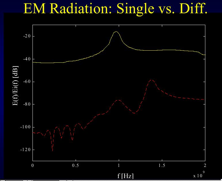
33 Loss of Transmission Lines Typically, dielectric loss is quite small -> G =. Thus Z where x R jwc jwl L C ( 1 jx) r ( R jwl )( jwc ) a j R wl 1/ 2 Highly Lossy w R L Near Lossless w Lossless case : x = Near Lossless: x << 1 Highly Lossy: x >> 1 w 33
34 Loss of Transmission Lines For Lossless case: a Z L C L C Time delay T L C Z For Near Lossless case: a 2 L R L C L C / C F HG L NM 1 Time delay T x O QP R j 2wL L C I KJ L 1 where C 2T / R C jwc 34
35 Loss of Transmission Lines For highly loss case: (RC transmission line) a Z wr C 2 wr C 2 R 2wC 1 [ 1 ] 2x 1 [ 1 ] 2x 1 [ 1 ] 2x That s why telephone company terminate the lines with 6 ohm Nonlinear phase relationship with f introduces signal distortion Example of RC transmission line: AWG 24 telephone line in home Z F HG R iwl ( w) 648( 1 j) jwc where R. 42 / in L 1nH / in C 1pF / in 1/ 2 I KJ w 1, rad / s( 16Hz) : voice band 35

36 Loss of Transmission Lines ( Dielectric Loss) The loss of dielectric loss is described by the loss tangent tan D G FR4 PCB tan D 35. wc GZ a D ( wc tan DZ) / 2 f tan D LC 2 36
37 Loss of Transmission Lines (Skin Effect) Skin Effect DC resistance AC resistance 37
, R(w) w R( w) / wl ( 1/ w) 1")
38 Loss of Transmission Lines (Skin Effect) s 1 2 a w Rw 1 length w ( ) area NOTE: In the near lossless region ( the characteristic impedance Z is not much affected by the skin effect R / wl 1), R(w) w R( w) / wl ( 1/ w) 1 38
39 Loss of Transmission Lines (Skin Effect) f (MHz) 1 s f R s ( ) Trace resistance um 4.7um 3.3um 2.4um 1.9um 1.7um 1.5um 2.6m ohm 3.7m ohm 5.2m ohm 7.4m ohm 9.m ohm 1.8m ohm 11.6m ohm ohm ohm ohm ohm ohm ohm ohm 6mil Cu 17um Skin depth resistance R = s = H / m 7 ( Cu) = S / m Length of trace = 2cm f ( ) 39
40 Loss Example: Gigabit differential transmission lines For comparison: (Set Conditions) 1. Differential impedance = 1 2. Trace width fixed to 8mil 3. Coupling coefficient = 5% 4. Metal : 1 oz Copper Question: 1. Which one has larger loss by skin effect? 2. Which one has larger loss of dielectric? 4


41 Loss Example: Gigabit differential transmission lines Skin effect loss 41
42 Loss Example: Gigabit differential transmission lines Skin effect loss Why? 42


43 Loss Example: Gigabit differential transmission lines Look at the field distribution of the common-mode coupling Coplanar structure has more surface for current flowing 43
44 Loss Example: Gigabit differential transmission lines How about the dielectric loss? Which one is larger? 44
45 Loss Example: Gigabit differential transmission lines The answer is dual stripline has larger loss. Why? The field density in the dielectric between the trace and GND is higher for dual stripline. 45
46 Loss Example: Gigabit differential transmission lines Which one has higher ability of rejecting common-mode noise? 46
47 Loss Example: Gigabit differential transmission lines The answer is coplanar stripline. Why? 47
48 48
49 49
50 5
51 51

52 Intuitive concept to determine Z and T d How physical dimensions affect impedance and delay Sensitivity is defined as percent change in impedance per percent change in line width, log-log plot shows sensitivity directly. Z is mostly influenced by w / h, the sensitivity is about 1%. It means 1% change in w / h will cause 1% change of Z The sensitivity of Z to changes in is about 4% r 52


53 Intuitive concept to determine Z and T d Striplines impedance Delay 53
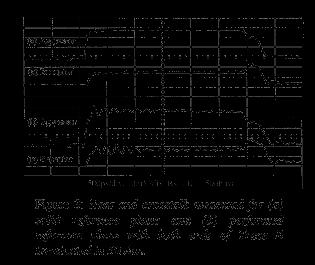
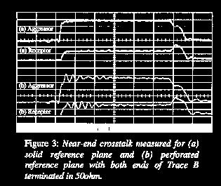
54 Ground Perforation: BGA via and impedance 54
55 Ground Perforation: Cross-talk (near end) 55
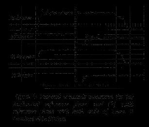
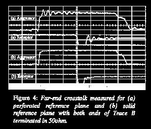
56 Ground Perforation : Cross-talk (far end) 56

57 Example(II): Transmission line on non-ideal GND Reasons for splits or slits on GND planes 57

58 Example(II): Transmission line on non-ideal GND 58

59 Example(II): Transmission line on non-ideal GND 59

60 Example(II): Transmission line on non-ideal GND 6

61 Example(II): Transmission line on non-ideal GND 61

62 Example(II): Transmission line on non-ideal GND 62

63 Example(II): Transmission line on non-ideal GND 63

64 Input side 64

65 Output side 65
66 66
67 67
68 68


69 Example: Rambus RDRAM and RIMM Design RDRAM Signal Routing 69
70 Example: Rambus RDRAM and RIMM Design Power: VDD = 2.5V, Vterm = 1.8V, Vref = 1.4V Signal:.8V Swing: Logic -> 1.8V, Logic 1 -> 1.V 2x4MHz CLK: 1.25ns timing window, 2ps rise/fall time Timing Skew: only allow 15ps - 2ps Rambus channel architecture: (3 controlled impedance and matched transmission lines) Two 9-bit data buses (DQA and DQB) A 3-bit ROW bus A 5-bit COL bus CTM and CFM differential clock buses 7

71 Example: Rambus RDRAM and RIMM Design RDRAM Channel is designed for 28 +/- 1% Impedance mismatch causes signal reflections Reflections reduce voltage and timing margins PCB process variation -> Z variation -> Channel error 71


72 Example: Rambus RDRAM and RIMM Design Intel suggested coplanar structure Ground flood & Stitch Intel suggested strip structure Ground flood & Stitch 72

73 Example: Rambus RDRAM and RIMM Design PCB Parameter sensitivity: H tolerance is hardest to control W & T have less impact on Z 73
74 Example: Rambus RDRAM and RIMM Design How to design Rambus channel in RIMM Module with uniform Z = 28 ohm?? How to design Rambus channel in RIMM Module with propagation delay variation in +/- 2ps?? 74

 Loaded trace Unloaded")
75 Example: Rambus RDRAM and RIMM Design Impedance Control: (Why?) Loaded trace Unloaded trace Connector 75
76 Example: Rambus RDRAM and RIMM Design Multi-drop Buses Unloaded Z Stub Device input Capacitance C d Equivalent loaded Z L Electric pitch L A Multidrop Bus Z L L C T C L L L L Z 2 28 (for Rambus design) where C is the per - unit - length equivalent capacitance at length L, T including the loading capacitance and the unloaded trace capacitance C is the loading capacitance including the device input capacitance C L d, the stub trace capacitance, and the via effect. 76
77 Example: Rambus RDRAM and RIMM Design In typical RIMM module design stub via Device input capacitance If C L. 2pF +.1pF + 2.2pF, and If you design unloaded trace Z the electric pitch L = 7.6mm to reach loaded Z 56 L 28 L C T Z psec / mm = 379 ph / mm = 9.5 ph / mil CL L 2. 5pF 379 ph / mm. 475 pf / mm 2 2 L Z 7. 6mm 56 L Z L C T 77
 If device pitch > electric pitch, modulation trace of 28ohm should be used. Modulation trace length = Device pitch Electric pitch 78")
78 Example: Rambus RDRAM and RIMM Design Modulation trace Device pitch = Device height + Device space Electrical pitch L is designed as L C Z L 2 L ( Z Z 2 Z 2 L ) If device pitch > electric pitch, modulation trace of 28ohm should be used. Modulation trace length = Device pitch Electric pitch 78
79 Example: Rambus RDRAM and RIMM Design Effect of PCB parameter variations on three key module electric characteristics 79
 2. Compensate each bend by a.3ps delay line.")
80 Example: Rambus RDRAM and RIMM Design Controlling propagation delay: Bend compensation Via Compensation Connector compensation Bend Compensation Rule of thumb:.3ps faster delay of every bend Solving strategies: 1. Using same numbers of bends for those critical traces(difficult) 2. Compensate each bend by a.3ps delay line. 8
81 Example: Rambus RDRAM and RIMM Design Via Compensation (delay) For a 8 layers PCB, a via with 5mil length can be modeled as (L, C) = (.485nH,.385pF). Delay T LC 137. psec Impedance Z = 1 LC 38 Inductive Rule of thumb: delay of a specific via depth can be calculated by scaling the inductance value which is proportional to via length. 3mil 3mil via has delay psec 5mil This delay difference can be compensated by adding a 1.566mm to the unloaded trace (56 ) 81

82 Example: Rambus RDRAM and RIMM Design Via Compensation (impedance) 82
83 Example: Rambus RDRAM and RIMM Design Connector Compensation 83


84 Example: EMI resulting from a trace near a PCB edge Experiment setup and trace design 84


85 Example: EMI resulting from a trace near a PCB edge Measurement Setup 85


86 Example: EMI resulting from a trace near a PCB edge EMI caused by Common-mode current : magnetic coupling Measured by current probe 86


87 Example: EMI resulting from a trace near a PCB edge EMI measured by the monopole : E field Low effect at high frequency 87


88 Example: EMI resulting from a trace near a PCB edge Trace height effect on EMI 88
89 Reference 1. Howard W. Johnson, High-speed digital design, Prentice-Hall, Ron K. Poon, Computer Circuits Electrical Design, Prentice-Hall, David M. Pozar, Microwave Engineering, John Wiley & Sons, William J. Dally, Digital System Engineering, Cambridge, Rambus, Direct Rambus RIMM Module Design Guide, V..9,
Microwave Engineering 3e Author - D. Pozar
 Microwave Engineering 3e Author - D. Pozar Sections 3.6 3.8 Presented by Alex Higgins 1 Outline Section 3.6 Surface Waves on a Grounded Dielectric Slab Section 3.7 Stripline Section 3.8 Microstrip An Investigation
ESE 570: Digital Integrated Circuits and VLSI Fundamentals
 ESE 570: Digital Integrated Circuits and VLSI Fundamentals Lec 24: April 19, 2018 Crosstalk and Wiring, Transmission Lines Lecture Outline! Crosstalk! Repeaters in Wiring! Transmission Lines " Where transmission
! Crosstalk. ! Repeaters in Wiring. ! Transmission Lines. " Where transmission lines arise? " Lossless Transmission Line.
 ESE 570: Digital Integrated Circuits and VLSI Fundamentals Lec 24: April 19, 2018 Crosstalk and Wiring, Transmission Lines Lecture Outline! Crosstalk! Repeaters in Wiring! Transmission Lines " Where transmission
Transient Response of Transmission Lines and TDR/TDT
 Transient Response of Transmission Lines and TDR/TDT Tzong-Lin Wu, Ph.D. EMC Lab. Department of Electrical Engineering National Sun Yat-sen University Outlines Why do we learn the transient response of
TC 412 Microwave Communications. Lecture 6 Transmission lines problems and microstrip lines
 TC 412 Microwave Communications Lecture 6 Transmission lines problems and microstrip lines RS 1 Review Input impedance for finite length line Quarter wavelength line Half wavelength line Smith chart A
Transmission Line Basics II - Class 6
 Transmission Line Basics II - Class 6 Prerequisite Reading assignment: CH2 Acknowledgements: Intel Bus Boot Camp: Michael Leddige Agenda 2 The Transmission Line Concept Transmission line equivalent circuits
and Ee = E ; 0 they are separated by a dielectric material having u = io-s S/m, µ, = µ, 0
 602 CHAPTER 11 TRANSMISSION LINES 11.10 Two identical pulses each of magnitude 12 V and width 2 µs are incident at t = 0 on a lossless transmission line of length 400 m terminated with a load. If the two
ECE 497 JS Lecture -03 Transmission Lines
 ECE 497 JS Lecture -03 Transmission Lines Spring 2004 Jose E. Schutt-Aine Electrical & Computer Engineering University of Illinois jose@emlab.uiuc.edu 1 MAXWELL S EQUATIONS B E = t Faraday s Law of Induction
ECE 451 Advanced Microwave Measurements. TL Characterization
 ECE 451 Advanced Microwave Measurements TL Characterization Jose E. Schutt-Aine Electrical & Computer Engineering University of Illinois jesa@illinois.edu ECE 451 Jose Schutt-Aine 1 Maxwell s Equations
Lecture Outline 9/27/2017. EE 4347 Applied Electromagnetics. Topic 4a
 9/7/17 Course Instructor Dr. Raymond C. Rumpf Office: A 337 Phone: (915) 747 6958 E Mail: rcrumpf@utep.edu EE 4347 Applied Electromagnetics Topic 4a Transmission Lines Transmission These Lines notes may
Transmission Lines. Plane wave propagating in air Y unguided wave propagation. Transmission lines / waveguides Y. guided wave propagation
 Transmission Lines Transmission lines and waveguides may be defined as devices used to guide energy from one point to another (from a source to a load). Transmission lines can consist of a set of conductors,
Analytic Solutions for Periodically Loaded Transmission Line Modeling
 Analytic Solutions for Periodically Loaded Transmission Line Modeling Paul G. Huray, huray@sc.edu Priya Pathmanathan, Intel priyap@qti.qualcomm.com Steve Pytel, Intel steve.pytel@ansys.com April 4, 2014
EELE 3332 Electromagnetic II Chapter 11. Transmission Lines. Islamic University of Gaza Electrical Engineering Department Dr.
 EEE 333 Electromagnetic II Chapter 11 Transmission ines Islamic University of Gaza Electrical Engineering Department Dr. Talal Skaik 1 1 11.1 Introduction Wave propagation in unbounded media is used in
ECEN720: High-Speed Links Circuits and Systems Spring 2017
 ECEN70: High-Speed Links Circuits and Systems Spring 07 Lecture : Channel Components, Wires, & Transmission Lines Sam Palermo Analog & Mixed-Signal Center Texas A&M University Announcements Lab Lab begins
Non-Sinusoidal Waves on (Mostly Lossless)Transmission Lines
Transmission Lines") Non-Sinusoidal Waves on (Mostly Lossless)Transmission Lines Don Estreich Salazar 21C Adjunct Professor Engineering Science October 212 https://www.iol.unh.edu/services/testing/sas/tools.php 1 Outline of
Non-Sinusoidal Waves on (Mostly Lossless)Transmission Lines Don Estreich Salazar 21C Adjunct Professor Engineering Science October 212 https://www.iol.unh.edu/services/testing/sas/tools.php 1 Outline of
INTRODUCTION TO TRANSMISSION LINES DR. FARID FARAHMAND FALL 2012
 INTRODUCTION TO TRANSMISSION LINES DR. FARID FARAHMAND FALL 2012 http://www.empowermentresources.com/stop_cointelpro/electromagnetic_warfare.htm RF Design In RF circuits RF energy has to be transported
Kimmo Silvonen, Transmission lines, ver
 Kimmo Silvonen, Transmission lines, ver. 13.10.2008 1 1 Basic Theory The increasing operating and clock frequencies require transmission line theory to be considered more and more often! 1.1 Some practical
ELECTROMAGNETISM SUMMARY. Maxwell s equations Transmission lines Transmission line transformers Skin depth
 ELECTROMAGNETISM SUMMARY Maxwell s equations Transmission lines Transmission line transformers Skin depth 1 ENGN4545/ENGN6545: Radiofrequency Engineering L#4 Magnetostatics: The static magnetic field Gauss
Differential Impedance finally made simple
 Slide - Differential Impedance finally made simple Eric Bogatin President Bogatin Enterprises 93-393-305 eric@bogent.com Slide -2 Overview What s impedance Differential Impedance: a simple perspective
SRAM System Design Guidelines
 Introduction This application note examines some of the important system design considerations an engineer should keep in mind when designing with Cypress SRAMs. It is important to note that while they
Transmission Lines. Author: Michael Leddige
 Transmission Lines Author: Michael Leddige 1 Contents PCB Transmission line structures Equivalent Circuits and Key Parameters Lossless Transmission Line Analysis Driving Reflections Systems Reactive Elements
Microwave Network Analysis
 Prof. Dr. Mohammad Tariqul Islam titareq@gmail.my tariqul@ukm.edu.my Microwave Network Analysis 1 Text Book D.M. Pozar, Microwave engineering, 3 rd edition, 2005 by John-Wiley & Sons. Fawwaz T. ILABY,
GMII Electrical Specification Options. cisco Systems, Inc.
 DC Specifications GMII Electrical Specification Options Mandatory - Communication between the transmitter and receiver can not occur at any bit rate without DC specifications. AC Specifications OPTION
EECS 117 Lecture 3: Transmission Line Junctions / Time Harmonic Excitation
 EECS 117 Lecture 3: Transmission Line Junctions / Time Harmonic Excitation Prof. Niknejad University of California, Berkeley University of California, Berkeley EECS 117 Lecture 3 p. 1/23 Transmission Line
ECEN689: Special Topics in High-Speed Links Circuits and Systems Spring 2012
 ECEN689: Special Topics in High-Speed Links Circuits and Systems Spring 0 Lecture : Channel Components, Wires, & Transmission Lines Sam Palermo Analog & Mixed-Signal Center Texas A&M University Announcements
UNIT I ELECTROSTATIC FIELDS
 UNIT I ELECTROSTATIC FIELDS 1) Define electric potential and potential difference. 2) Name few applications of gauss law in electrostatics. 3) State point form of Ohm s Law. 4) State Divergence Theorem.
Omar M. Ramahi University of Waterloo Waterloo, Ontario, Canada
 Omar M. Ramahi University of Waterloo Waterloo, Ontario, Canada Traditional Material!! Electromagnetic Wave ε, μ r r The only properties an electromagnetic wave sees: 1. Electric permittivity, ε 2. Magnetic
PHY3128 / PHYM203 (Electronics / Instrumentation) Transmission Lines
 Transmission Lines") Transmission Lines Introduction A transmission line guides energy from one place to another. Optical fibres, waveguides, telephone lines and power cables are all electromagnetic transmission lines. are
Transmission Lines Introduction A transmission line guides energy from one place to another. Optical fibres, waveguides, telephone lines and power cables are all electromagnetic transmission lines. are
Topic 5: Transmission Lines
 Topic 5: Transmission Lines Profs. Javier Ramos & Eduardo Morgado Academic year.13-.14 Concepts in this Chapter Mathematical Propagation Model for a guided transmission line Primary Parameters Secondary
Transmission Lines. Transmission lines. Telegraphist Equations. Reflection Coefficient. Transformation of voltage, current and impedance
 Transmission Lines Transmission lines Telegraphist Equations Reflection Coefficient Transformation of voltage, current and impedance Application of trasnmission lines 1 ENGN4545/ENGN6545: Radiofrequency
AN B. Basic PCB traces transmission line effects causing signal integrity degradation simulation using Altium DXP version 6.
 AN200805-01B Basic PCB traces transmission line effects causing signal integrity degradation simulation using Altium DXP version 6.9 By Denis Lachapelle eng. and Anne Marie Coutu. May 2008 The objective
TASK A. TRANSMISSION LINE AND DISCONTINUITIES
 TASK A. TRANSMISSION LINE AND DISCONTINUITIES Task A. Transmission Line and Discontinuities... 1 A.I. TEM Transmission Line... A.I.1. Circuit Representation of a Uniform Transmission Line... A.I.. Time
Accounting for High Frequency Transmission Line Loss Effects in HFSS. Andrew Byers Tektronix
 Accounting for High Frequency Transmission Line Loss Effects in HFSS Andrew Byers Tektronix Transmission Line Refresher γ = α + j β = (R + jωl) * (G + jωc) Zo = Zr + j Zi = (R + jωl) / (G + jωc) Transmission
SI Surging Ideas TVS Diode Application Note PROTECTION PRODUCTS. Layout Guidelines for adding ESD Protection in HDMI Receiver Applications
 Layout Guidelines for adding ESD Protection in HDMI Receiver Applications The High Definition Multimedia Interface (HDMI) video signals are transmitted on very high speed differential pairs. These lines
Lecture 23. Dealing with Interconnect. Impact of Interconnect Parasitics
 Lecture 23 Dealing with Interconnect Impact of Interconnect Parasitics Reduce Reliability Affect Performance Classes of Parasitics Capacitive Resistive Inductive 1 INTERCONNECT Dealing with Capacitance
Introduction to RF Design. RF Electronics Spring, 2016 Robert R. Krchnavek Rowan University
 Introduction to RF Design RF Electronics Spring, 2016 Robert R. Krchnavek Rowan University Objectives Understand why RF design is different from lowfrequency design. Develop RF models of passive components.
ECE414/514 Electronics Packaging Spring 2012 Lecture 6 Electrical D: Transmission lines (Crosstalk) Lecture topics
 Lecture topics") ECE414/514 Electronics Packaging Spring 2012 Lecture 6 Electrical D: Transmission lines (Crosstalk) James E. Morris Dept of Electrical & Computer Engineering Portland State University 1 Lecture topics
ECE414/514 Electronics Packaging Spring 2012 Lecture 6 Electrical D: Transmission lines (Crosstalk) James E. Morris Dept of Electrical & Computer Engineering Portland State University 1 Lecture topics
ECE 451 Transmission Lines & Packaging
 Transmission Lines & Packaging Jose E. Schutt-Aine Electrical & Computer Engineering University of Illinois jose@emlab.uiuc.edu 1 Radio Spectrum Bands The use of letters to designate bands has long ago
TL/Finite Length. 2Vi. What happens when a traveling wave reaches the end of a transmission line?
 TL/Finite Length What happens when a traveling wave reaches the end of a transmission line? Vi Vi Vi Ir If It Zt Zt Thought Process: Transmission line with impedance Cut open Develop TEC for open transmission
EMC Considerations for DC Power Design
 EMC Considerations for DC Power Design Tzong-Lin Wu, Ph.D. Department of Electrical Engineering National Sun Yat-sen University Power Bus Noise below 5MHz 1 Power Bus Noise below 5MHz (Solution) Add Bulk
EE141-Spring 2008 Digital Integrated Circuits EE141. Announcements EECS141 EE141. Lecture 24: Wires
 EE141-Spring 2008 Digital Integrated Circuits Lecture 24: Wires 1 Announcements Hw 8 posted last graded homework Project phase II feedback to be expected anytime 2 Material Last Lecture: Wire capacitance
Equivalent Circuit Model Extraction for Interconnects in 3D ICs
 Equivalent Circuit Model Extraction for Interconnects in 3D ICs A. Ege Engin Assistant Professor, Department of ECE, San Diego State University Email: aengin@mail.sdsu.edu ASP-DAC, Jan. 23, 213 Outline
Transmission-Line Essentials for Digital Electronics
 C H A P T E R 6 Transmission-Line Essentials for Digital Electronics In Chapter 3 we alluded to the fact that lumped circuit theory is based on lowfrequency approximations resulting from the neglect of
TECHNO INDIA BATANAGAR
 TECHNO INDIA BATANAGAR ( DEPARTMENT OF ELECTRONICS & COMMUNICATION ENGINEERING) QUESTION BANK- 2018 1.Vector Calculus Assistant Professor 9432183958.mukherjee@tib.edu.in 1. When the operator operates on
INSTITUTE OF AERONAUTICAL ENGINEERING Dundigal, Hyderabad Electronics and Communicaton Engineering
 INSTITUTE OF AERONAUTICAL ENGINEERING Dundigal, Hyderabad - 00 04 Electronics and Communicaton Engineering Question Bank Course Name : Electromagnetic Theory and Transmission Lines (EMTL) Course Code :
Nonideal Conductor Models
 Nonideal Conductor Models 吳瑞北 Rm. 340, Department of Electrical Engineering E-mail: rbwu@ew.ee.ntu.edu.tw url: cc.ee.ntu.edu.tw/~rbwu S. H. Hall et al., High-Speed Digital Designs, Chap.5 1 What will You
Lecture Outline. Attenuation Coefficient and Phase Constant Characteristic Impedance, Z 0 Special Cases of Transmission Lines
 Course Instructor Dr. Raymond C. Rumpf Office: A 337 Phone: (915) 747 6958 E Mail: rcrumpf@utep.edu EE 4347 Applied Electromagnetics Topic 4b Transmission Line Parameters Transmission These Line notes
A New, Accurate Quasi-Static Model for Conductor Loss in Coplanar Waveguide
 A New, Accurate Quasi-Static Model for Conductor Loss in Coplanar Waveguide M. S. Islam, E. Tuncer, D. P. Neikirk Dept. of Electrical & Computer Engineering Austin, Texas Conductor loss calculation techniques
Time Domain Modeling of Lossy Interconnects
 IEEE TRANSACTIONS ON ADVANCED PACKAGING, VOL. 24, NO. 2, MAY 2001 191 Time Domain Modeling of Lossy Interconnects Christer Svensson, Member, IEEE, and Gregory E. Dermer Abstract A new model for dielectric
Power Distribution Network Design for High-Speed Printed Circuit Boards
 Power Distribution Network Design for High-Speed Printed Circuit Boards Jun Fan NCR Corporation 1 Outline Overview of PDN design in multi-layer PCBs Interconnect Inductance Individual Capacitor Values
SCSI Connector and Cable Modeling from TDR Measurements
 SCSI Connector and Cable Modeling from TDR Measurements Dima Smolyansky TDA Systems, Inc. http://www.tdasystems.com Presented at SCSI Signal Modeling Study Group Rochester, MN, December 1, 1999 Outline
5/1/2011 V R I. = ds. by definition is the ratio of potential difference of the wire ends to the total current flowing through it.
 Session : Fundamentals by definition is the ratio of potential difference of the wire ends to the total current flowing through it. V R I E. dl L = σ E. ds A R = L σwt W H T At high frequencies, current
MM74C150 MM82C19 16-Line to 1-Line Multiplexer 3-STATE 16-Line to 1-Line Multiplexer
 MM74C150 MM82C19 16-Line to 1-Line Multiplexer 3-STATE 16-Line to 1-Line Multiplexer General Description The MM74C150 and MM82C19 multiplex 16 digital lines to 1 output. A 4-bit address code determines
Modeling frequency-dependent conductor losses and dispersion in serial data channel interconnects
 Modeling frequency-dependent conductor losses and dispersion in serial data channel interconnects Yuriy Shlepnev Simberian Inc., www.simberian.com Abstract: Models of transmission lines and transitions
Announcements. EE141- Fall 2002 Lecture 25. Interconnect Effects I/O, Power Distribution
 - Fall 2002 Lecture 25 Interconnect Effects I/O, Power Distribution Announcements Homework 9 due next Tuesday Hardware lab this week Project phase 2 due in two weeks 1 Today s Lecture Impact of interconnects»
COURTESY IARE. Code No: R R09 Set No. 2
 Code No: R09220404 R09 Set No. 2 II B.Tech II Semester Examinations,APRIL 2011 ELECTRO MAGNETIC THEORY AND TRANSMISSION LINES Common to Electronics And Telematics, Electronics And Communication Engineering,
ECE 107: Electromagnetism
 ECE 107: Electromagnetism Set 2: Transmission lines Instructor: Prof. Vitaliy Lomakin Department of Electrical and Computer Engineering University of California, San Diego, CA 92093 1 Outline Transmission
Spectral Domain Analysis of Open Planar Transmission Lines
 Mikrotalasna revija Novembar 4. Spectral Domain Analysis of Open Planar Transmission Lines Ján Zehentner, Jan Mrkvica, Jan Macháč Abstract The paper presents a new code calculating the basic characteristics
Effects from the Thin Metallic Substrate Sandwiched in Planar Multilayer Microstrip Lines
 Progress In Electromagnetics Research Symposium 2006, Cambridge, USA, March 26-29 115 Effects from the Thin Metallic Substrate Sandwiched in Planar Multilayer Microstrip Lines L. Zhang and J. M. Song Iowa
Surface Mount Chip Capacitors
 Features High '' Factor at high frequencies High RF power capabilities Low High self resonant frequencies Excellent stability across temperature range Small size High Frequency Measurement and Performance
Contents. Transmission Lines The Smith Chart Vector Network Analyser (VNA) ü structure ü calibration ü operation. Measurements
 ü structure ü calibration ü operation. Measurements") Contents Transmission Lines The Smith Chart Vector Network Analyser (VNA) ü structure ü calibration ü operation Measurements Göran Jönsson, EIT 2015-04-27 Vector Network Analysis 2 Waves on Lines If the
Contents Transmission Lines The Smith Chart Vector Network Analyser (VNA) ü structure ü calibration ü operation Measurements Göran Jönsson, EIT 2015-04-27 Vector Network Analysis 2 Waves on Lines If the
Five Myths about the PDN
 Slide -1 A copy of the slides is available on www.bethesignal.com: search VL-180 or PPT-180 Five Myths about the PDN Eric Bogatin, eric@bethesignal.com Signal Integrity Evangelist Bogatin Enterprises www.bethesignal.com
Contents. Transmission Lines The Smith Chart Vector Network Analyser (VNA) ü structure ü calibration ü operation. Measurements
 ü structure ü calibration ü operation. Measurements") Contents Transmission Lines The Smith Chart Vector Network Analyser (VNA) ü structure ü calibration ü operation Measurements Göran Jönsson, EIT 2017-05-12 Vector Network Analysis 2 Waves on Lines If the
Contents Transmission Lines The Smith Chart Vector Network Analyser (VNA) ü structure ü calibration ü operation Measurements Göran Jönsson, EIT 2017-05-12 Vector Network Analysis 2 Waves on Lines If the
Signal integrity in deep-sub-micron integrated circuits
 Signal integrity in deep-sub-micron integrated circuits Alessandro Bogliolo abogliolo@ing.unife.it Outline Introduction General signaling scheme Noise sources and effects in DSM ICs Supply noise Synchronization
Understanding EMC Basics
 1of 7 series Webinar #1 of 3, February 27, 2013 EM field theory, and 3 types of EM analysis Webinar Sponsored by: EurIng CEng, FIET, Senior MIEEE, ACGI AR provides EMC solutions with our high power RF/Microwave
Broadband transmission line models for analysis of serial data channel interconnects
 PCB Design Conference East, Durham NC, October 23, 2007 Broadband transmission line models for analysis of serial data channel interconnects Y. O. Shlepnev, Simberian, Inc. shlepnev@simberian.com Simberian:
Electrostatics: Electrostatic Devices
 Electrostatics: Electrostatic Devices EE331 Electromagnetic Field Theory Outline Laplace s Equation Derivation Meaning Solving Laplace s equation Resistors Capacitors Electrostatics -- Devices Slide 1
A Method to Extract Dielectric Parameters from Transmission Lines with Conductor Surface Roughness at Microwave Frequencies
 Progress In Electromagnetics Research M, Vol. 48, 1 8, 2016 A Method to Extract Dielectric Parameters from Transmission Lines with Conductor Surface Roughness at Microwave Frequencies Binke Huang * and
AC Circuits. The Capacitor
 The Capacitor Two conductors in close proximity (and electrically isolated from one another) form a capacitor. An electric field is produced by charge differences between the conductors. The capacitance
RECENT ADVANCES in NETWORKING, VLSI and SIGNAL PROCESSING
 Optimization of Reflection Issues in High Speed Printed Circuit Boards ROHITA JAGDALE, A.VENU GOPAL REDDY, K.SUNDEEP Department of Microelectronics and VLSI Design International Institute of Information
ECE 497 JS Lecture - 18 Noise in Digital Circuits
 ECE 497 JS Lecture - 18 Noise in Digital Circuits Spring 2004 Jose E. Schutt-Aine Electrical & Computer Engineering University of Illinois jose@emlab.uiuc.edu 1 Announcements Thursday April 15 th Speaker:
Name. Section. Short Answer Questions. 1. (20 Pts) 2. (10 Pts) 3. (5 Pts) 4. (10 Pts) 5. (10 Pts) Regular Questions. 6. (25 Pts) 7.
 2. (10 Pts) 3. (5 Pts) 4. (10 Pts) 5. (10 Pts) Regular Questions. 6. (25 Pts) 7.") Name Section Short Answer Questions 1. (20 Pts) 2. (10 Pts) 3. (5 Pts). (10 Pts) 5. (10 Pts) Regular Questions 6. (25 Pts) 7. (20 Pts) Notes: 1. Please read over all questions before you begin your work.
Name Section Short Answer Questions 1. (20 Pts) 2. (10 Pts) 3. (5 Pts). (10 Pts) 5. (10 Pts) Regular Questions 6. (25 Pts) 7. (20 Pts) Notes: 1. Please read over all questions before you begin your work.
Lecture 25. Dealing with Interconnect and Timing. Digital Integrated Circuits Interconnect
 Lecture 25 Dealing with Interconnect and Timing Administrivia Projects will be graded by next week Project phase 3 will be announced next Tu.» Will be homework-like» Report will be combined poster Today
EKT 356 MICROWAVE COMMUNICATIONS CHAPTER 2: PLANAR TRANSMISSION LINES
 EKT 356 MICROWAVE COMMUNICATIONS CHAPTER : PLANAR TRANSMISSION LINES 1 Tansmission Lines A device used to tansfe enegy fom one point to anothe point efficiently Efficiently minimum loss, eflection and
Module 2 : Transmission Lines. Lecture 1 : Transmission Lines in Practice. Objectives. In this course you will learn the following
 Objectives In this course you will learn the following Point 1 Point 2 Point 3 Point 4 Point 5 Point 6 Point 7 Point 8 Point 9 Point 10 Point 11 Point 12 Various Types Of Transmission Line Explanation:
Solutions to Problems in Chapter 6
 Appendix F Solutions to Problems in Chapter 6 F.1 Problem 6.1 Short-circuited transmission lines Section 6.2.1 (book page 193) describes the method to determine the overall length of the transmission line
PCB Project: Measuring Package Bond-Out Inductance via Ground Bounce
 PCB Project: Measuring Package Bond-Out Inductance via Ground Bounce Kylan Roberson July 9, 014 Abstract In this experiment I looked into a way of measuring the ground bounce generated by capacitively
ANTENNAS and MICROWAVES ENGINEERING (650427)
") Philadelphia University Faculty of Engineering Communication and Electronics Engineering ANTENNAS and MICROWAVES ENGINEERING (65427) Part 2 Dr. Omar R Daoud 1 General Considerations It is a two-port network
Philadelphia University Faculty of Engineering Communication and Electronics Engineering ANTENNAS and MICROWAVES ENGINEERING (65427) Part 2 Dr. Omar R Daoud 1 General Considerations It is a two-port network
Improving Power Delivery Networks (PDNs) Using Polyimide-based Thin Laminates
 Using Polyimide-based Thin Laminates") Improving Power Delivery Networks (PDNs) Using Polyimide-based Thin Laminates 2017. 7. 19. 1 Contents 1. Embedded passives technology 2. Thin laminates: material choices and applications 3. Buried capacitance
Improving Power Delivery Networks (PDNs) Using Polyimide-based Thin Laminates 2017. 7. 19. 1 Contents 1. Embedded passives technology 2. Thin laminates: material choices and applications 3. Buried capacitance
INTEGRATED CIRCUITS. 74ALS11A Triple 3-Input AND gate. Product specification 1991 Feb 08 IC05 Data Handbook
 INTEGRATED CIRCUITS Triple 3-Input AND gate 1991 Feb 08 IC05 Data Handbook TYPE TYPICAL PROPAGATION DELAY TYPICAL SUPPLY CURRENT (TOTAL) 5.5ns 1.3mA PIN CONFIGURATION 1A 1 1B 2 14 13 V CC 1C ORDERING INFORMATION
A Novel Tunable Dual-Band Bandstop Filter (DBBSF) Using BST Capacitors and Tuning Diode
 Using BST Capacitors and Tuning Diode") Progress In Electromagnetics Research C, Vol. 67, 59 69, 2016 A Novel Tunable Dual-Band Bandstop Filter (DBBSF) Using BST Capacitors and Tuning Diode Hassan Aldeeb and Thottam S. Kalkur * Abstract A novel
Progress In Electromagnetics Research C, Vol. 67, 59 69, 2016 A Novel Tunable Dual-Band Bandstop Filter (DBBSF) Using BST Capacitors and Tuning Diode Hassan Aldeeb and Thottam S. Kalkur * Abstract A novel
1 Chapter 8 Maxwell s Equations
 Electromagnetic Waves ECEN 3410 Prof. Wagner Final Review Questions 1 Chapter 8 Maxwell s Equations 1. Describe the integral form of charge conservation within a volume V through a surface S, and give
Boundary and Excitation Training February 2003
 Boundary and Excitation Training February 2003 1 Why are They Critical? For most practical problems, the solution to Maxwell s equations requires a rigorous matrix approach such as the Finite Element Method
EECS 151/251A Spring 2018 Digital Design and Integrated Circuits. Instructors: Nick Weaver & John Wawrzynek. Lecture 12 EE141
 EECS 151/251A Spring 2018 Digital Design and Integrated Circuits Instructors: Nick Weaver & John Wawrzynek Lecture 12 1 Wire Models All-inclusive model Capacitance-only 2 Capacitance Capacitance: The Parallel
ECE 546 Lecture 13 Scattering Parameters
 ECE 546 Lecture 3 Scattering Parameters Spring 08 Jose E. Schutt-Aine Electrical & Computer Engineering University of Illinois jesa@illinois.edu ECE 546 Jose Schutt Aine Transfer Function Representation
ELECTROMAGNETISM. Second Edition. I. S. Grant W. R. Phillips. John Wiley & Sons. Department of Physics University of Manchester
 ELECTROMAGNETISM Second Edition I. S. Grant W. R. Phillips Department of Physics University of Manchester John Wiley & Sons CHICHESTER NEW YORK BRISBANE TORONTO SINGAPORE Flow diagram inside front cover
Your RF Cable, the unknown Entity
 HAM RADIO 2018 Your RF Cable, the unknown Entity PROF. DR. THOMAS BAIER E-mail: baier@hs-ulm.de DG8SAQ Hochschule Ulm University of Applied Sciences Prittwitzstrasse 10 89075 Ulm Thanks to: Dan Maguire
Rg2 Lg2 Rg6 Lg6 Rg7 Lg7. PCB Trace & Plane. Figure 1 Bypass Decoupling Loop
 TECHNICAL NOTE This article was originally published in 1996. INTRODUCTION In order to guarantee better performance from highspeed digital integrated circuits (ICs), manufacturers are tightening power
KINGS COLLEGE OF ENGINEERING DEPARTMENT OF ELECTRONICS AND COMMUNICATION ENGINEERING QUESTION BANK
 KINGS COLLEGE OF ENGINEERING DEPARTMENT OF ELECTRONICS AND COMMUNICATION ENGINEERING QUESTION BANK SUB.NAME : ELECTROMAGNETIC FIELDS SUBJECT CODE : EC 2253 YEAR / SEMESTER : II / IV UNIT- I - STATIC ELECTRIC
Switched-Capacitor Circuits David Johns and Ken Martin University of Toronto
 Switched-Capacitor Circuits David Johns and Ken Martin University of Toronto (johns@eecg.toronto.edu) (martin@eecg.toronto.edu) University of Toronto 1 of 60 Basic Building Blocks Opamps Ideal opamps usually
ECE 497 JS Lecture -07 Planar Transmission Lines
 ECE 497 JS Lecture -07 Planar Transmission Lines Spring 2004 Jose E. Schutt-Aine Electrical & Computer Engineering University of Illinois jose@emlab.uiuc.edu 1 Microstrip ε Z o w/h < 3.3 2 119.9 h h =
ECE 497 JS Lecture - 18 Impact of Scaling
 ECE 497 JS Lecture - 18 Impact of Scaling Spring 2004 Jose E. Schutt-Aine Electrical & Computer Engineering University of Illinois jose@emlab.uiuc.edu 1 Announcements Thursday April 8 th Speaker: Prof.
Causal Modeling and Extraction of Dielectric Constant and Loss Tangent for Thin Dielectrics
 Causal Modeling and Extraction of Dielectric Constant and Loss Tangent for Thin Dielectrics A. Ege Engin 1, Abdemanaf Tambawala 1, Madhavan Swaminathan 1, Swapan Bhattacharya 1, Pranabes Pramanik 2, Kazuhiro
9/18/2008 GMU, ECE 680 Physical VLSI Design
 ECE680: Physical VLSI Design Chapter III CMOS Device, Inverter, Combinational circuit Logic and Layout Part 3 Combinational Logic Gates (textbook chapter 6) 9/18/2008 GMU, ECE 680 Physical VLSI Design
Pulses in transmission lines
 Pulses in transmission lines Physics 401, Fall 2018 Eugene V. Colla Definition Distributed parameters network Pulses in transmission line Wave equation and wave propagation Reflections. Resistive load
Pulses in transmission lines
 Pulses in transmission lines Physics 401, Fall 013 Eugene V. Colla Definition Distributed parameters networ Pulses in transmission line Wave equation and wave propagation eflections. esistive load Thévenin's
Modeling copper cables and PCBs
 Chapter 2 Modeling copper cables and PCBs 2.1. Introduction A proper channel model is a good basis for a correct understanding of any transmission system. The goal of this chapter is to identify an accurate
High Speed Communication Circuits and Systems Lecture 4 Generalized Reflection Coefficient, Smith Chart, Integrated Passive Components
 High Speed Communication Circuits and Systems Lecture 4 Generalized Reflection Coefficient, Smith Chart, Integrated Passive Components Michael H. Perrott February 11, 2004 Copyright 2004 by Michael H.
Interconnects. Wire Resistance Wire Capacitance Wire RC Delay Crosstalk Wire Engineering Repeaters. ECE 261 James Morizio 1
 Interconnects Wire Resistance Wire Capacitance Wire RC Delay Crosstalk Wire Engineering Repeaters ECE 261 James Morizio 1 Introduction Chips are mostly made of wires called interconnect In stick diagram,
Contents. ! Transmission Lines! The Smith Chart! Vector Network Analyser (VNA) ! Measurements. ! structure! calibration! operation
 ! Measurements. ! structure! calibration! operation") Contents! Transmission Lines! The Smith Chart! Vector Network Analyser (VNA)! structure! calibration! operation! Measurements Göran Jönsson, EIT 2009-11-16 Network Analysis 2! Waves on Lines! If the wavelength
Contents! Transmission Lines! The Smith Chart! Vector Network Analyser (VNA)! structure! calibration! operation! Measurements Göran Jönsson, EIT 2009-11-16 Network Analysis 2! Waves on Lines! If the wavelength