SEMICONDUCTOR BEHAVIOR AND THE HALL EFFECT
|
|
|
- Charleen Scott
- 6 years ago
- Views:
Transcription
1 5 Feb 14 Semi.1 SEMICONDUCTOR BEHAVIOR AND THE HALL EFFECT The object of this experiment is to study various properties of n- and p-doped germanium crystals. The temperature dependence of the electrical conductivity, and the Hall Effect in germanium, will be demonstrated. The sign of the charge carriers responsible for conduction, the charge carrier concentration, and the charge carrier mobility will be determined for the two types of crystals. Theory: A rigorous treatment of the electrical behaviour of semiconductors involves the application of quantum mechanics through the Schrodinger equation and of statistical physics through the Fermi-Dirac distribution, and this is best left to a class in solid-state physics. In this discussion the free-electron and nearly-free-electron models will be used. Where necessary, results from solid-state physics will be presented without derivation and the reader is directed to the list of references at the end of this experiment for further information. The free-electron model Applying the Schrodinger equation to the relatively simple situation of a free electron confined within a solid yields quantization of the electron's momentum and hence energy. That is, the electron can only occupy certain energy levels. The electrons in a sample of material at very low temperature will fill the energy levels from the lowest on up so that the system is in its ground (lowest total energy) state. Any given energy level can contain at most two electrons, one with spin up and one with spin down (Pauli exclusion principle). The maximum energy an electron can have in the ground state is called the Fermi energy, E F. At zero temperature (0 K) all the electron energy states below the Fermi energy are occupied, and all those above are vacant. At finite temperature, the probability that an energy state is occupied is a function of energy and temperature, the Fermi-Dirac distribution. The effect of higher temperature is that electrons near the Fermi energy are able to 'jump' into unoccupied higher-energy states. Thus, the situation of filled and vacant states at T = 0 becomes one of filled, partially filled, and vacant states at T > 0. In discussing the electronic properties of materials the core electrons (those in completely filled orbits) play little or no role. It is the valence electrons, those from partially filled shells whose orbits encompass more than one atom, that most affect the properties of a material. The limits of the free-electron model can be shown by considering the situation when a voltage is applied across a sample in which the valence electrons are assumed to be free. If the sample has dimension in the direction of the applied voltage and cross section A, then the current I (rate of charge flow through the sample) and current density j = I/A are
2 5 Feb 14 Semi.2 I = n o eva (1) j = n o ev (2) where n o is the number density of valence electrons, e is the electronic charge, and v is the electron velocity. The applied voltage produces an electric field E. Since an electron at the Fermi energy can be considered free because of the unlimited empty energy states above it, the only force acting on the electron is that due to the applied electric field. F = ee (3) It should be immediately obvious that this model is incorrect. A constant force acting on the electron means constant acceleration, increasing electron velocity, and increasing current through the sample the longer the field is applied. This is contrary to experience whereby an applied voltage produces a constant current. Writing Ohm's Law in terms of conductivity,, current density, and electric field: = j/e = n o ev/e (4) The result of applying equation (3) is: = e 2 n o t/m (5) where t is the time that the voltage has been applied and m is the electron mass. This states that conductivity depends directly on the density of valence electrons, a reasonable statement. However, it also states that the conductivity increases with time!, a statement that does not make sense. The fault in this derivation lies in the assumption of free electrons. The valence electrons do in fact interact with the atoms of the material. This can be accounted for by assuming that the valence electrons move through the material, generally unaffected by the atoms, until a major interaction such as an elastic collision occurs. The equation derived using the free-electron model can be suitably modified by replacing t, the time for which the electric field has been applied, with, the mean time between interactions of the valence electron with the atoms of the material. = e 2 n o /m (6) Although not shown explicitly, is temperature dependent. An electron interacts with an atom only when it gets within a certain distance of it. At higher temperatures, the atom vibrates
3 5 Feb 14 Semi.3 around its equilibrium position as a result of its thermal energy. Thus it represents a fuzzy volume in space that is larger than the actual size of the atom and so at higher temperature an electron is more likely to interact with any particular atom. As a result the mean time between interactions,, becomes shorter and decreases with increasing temperature. [In the above expression it has been implicitly assumed that a single value for can be assigned to a given material at a specific temperature. In fact, depends on the energy of the electrons (charge carriers).] The substitution of the 'mean free time' in the conductivity equation is equivalent to assigning an average, steady, drift velocity, v D, to the valence electrons. Equation (4) becomes: = n o ev D /E (7) Defining the mobility,, as the drift velocity per unit electric field: = n o e (8) The nearly-free-electron model Although the modified free-electron model can account for the temperature dependence of the conductivity of conductors, it cannot account for the temperature dependence or the low values of the conductivities of semiconductors. A more realistic treatment of the effects of the atoms on the valence electrons is to substitute a position-dependent potential function into the Schrodinger equation. Because of the regular spacing of atoms in a solid, the atoms of the material (considered without their valence electrons) represent uniformly spaced, deep, attractive potential wells for the valence electrons. At certain values of electron momentum the electron wavefunction and thus the electron probability function have a zero at the location of each atom. When this occurs there are discontinuities in the electron energy distribution. These discontinuities are called energy gaps and there are no allowed states with energies in these regions. The size of the energy gaps depends on the details of the potential function V(x). The regions of allowed energy states are called energy bands. Because of this, this model is also known as the band theory of solids. Each band contains one energy level for each atom in the sample of material. Since each energy level can accommodate two electrons, at low temperature (T = 0) atoms with even numbers of valence electrons will have bands that are either completely filled or empty and atoms with odd numbers of valence electrons will have the upper band half-filled. In this simple band model the three factors that are important in determining the electronic properties of a material are: 1) the temperature, 2) the size of the energy gap,
4 5 Feb 14 Semi.4 3) the relative locations of the Fermi energy and the energy gap. In this experiment the behavior of germanium, a semiconductor, which has a valence of 4, will be studied. Consider a sample of pure germanium (intrinsic semiconductor). At low temperature the valence electrons are all in the two lowest bands, no electrons being in the third band. The highest occupied band is called the valence band and the lowest vacant band is called the conduction band. The population of the various energy levels in the valence and conduction bands can be shown graphically. Conduction Band E GAP E F Valence Band T = 0 T > 0 Figure 1 Electron energy increases vertically and the number of electrons in each energy level is shown horizontally. The solid line shows the Fermi-Dirac (F-D) distribution. At low temperature the F-D distribution is a step function between 0 and 2, centred at the Fermi energy. The valence band is completely filled and the conduction band is completely empty. Thus at low temperature the material behaves like an insulator. At higher temperature, the curvature of the F-D distribution shows the finite probability of some electrons from the higher levels of the valence band acquiring enough energy through thermal excitation to cross the energy gap and reach the allowed levels in the conduction band. Electrons that reach the conduction band behave like free electrons because of the unoccupied levels above them. Thus a semiconductor such as germanium at room temperature will conduct to a certain extent. Three factors of note are: 1. The number of electrons in the conduction band is relatively small compared to a pure conductor such as a metal. 2. The number of electrons in the conduction band is highly temperature dependent due to the temperature dependence of the F-D distribution. At higher temperature the F-D distribution broadens along the energy axis (higher energy levels become populated, lower energy levels
5 5 Feb 14 Semi.5 become vacated) and narrows along the probability axis (a wider spread of levels will be partially occupied). This increased number of conduction electrons with increased temperature 'overrides' the decrease of mean free time that occurs with increased temperature. As a result, the conductivity of a semiconductor increases with increased temperature contrary to the behavior of a conductor. 3. When an electron jumps into the conduction band it leaves a vacant state or 'hole' at the top of the valence band. The hole behaves like a positive charge and thus when an electric field is applied it can contribute to the conduction by interchanging energy states with an electron in the valence band. To reiterate the quantum nature of the conduction process: conduction in semiconductors at room temperature may take place via two distinct and independent quantum-mechanical modes of electron motion, which can most simply be described as classical conduction by 'conduction' electrons with charge e and effective mass m E *, and by holes with charge +e and effective mass m H *. This classical picture of holes and conduction electrons is possible only because the major quantum features of the electronic motions in the solid can be buried in the 'effective mass' parameter. To obtain a quantitative description of the conductivity of a semiconductor, equation (8) is used: = ne (8) where n is the number density, e is the charge, and is the mobility of the charge carrier. In a pure (intrinsic) semiconductor the number of electrons in the conduction band equals the number of holes in the valence band: The total conductivity is n E = n H (9) = n E e E + n H e H (10) = n E e( E + H (11) (addition because electrons and holes have opposite charge and move in opposite directions). n E is determined by integrating the F-D distribution over the occupied states in the conduction band. The result is 3 n UT e E GAP kt (12) E where U is a constant that depends on the density of electron states in the conduction band and k is the Boltzmann constant. Substituting for n E in equation (11) yields
6 5 Feb 14 Semi.6 3 GAP 2 2 2eU T e E kt ( ) E H (13) The effect of the T 3/2 factor is extremely small compared with that of the exponential factor. Therefore the expression for is often written as: ( constant) GAP e E kt 2 (14) A plot of ln( ) versus 1/T will be linear with slope E GAP /2k. If is measured as a function of temperature, the energy gap of the material can be determined. From Ohm s Law in terms of conductivity, current density, and electric field (equation (4)), for a sample of fixed size the conductivity is inversely proportional to the voltage drop across the sample if the current through the sample is kept constant: = j/e = I AE I 1 AV V where and A are the sample length and cross-sectional area respectively. Therefore, for constant current through the sample, a plot of ln(1/v) versus 1/T will be linear with slope E GAP /2k. To this point the discussion has concerned pure (intrinsic) semiconductors, for example a crystal of pure germanium. Of greater interest and importance is the behavior of extrinsic or doped semiconductors. A doped semiconducting device is made from a semiconductor such as germanium that contains a small amount of some impurity. Consider a germanium sample to which a small number of phosphorous atoms have been added. Phosphorous has a valence of 5 compared to germanium with a valence of 4. Four of the phosphorous valence electrons occupy levels in the germanium valence band. The energy level of the extra phosphorous valence electron is just below the conduction band of germanium; thus very little additional energy is needed for this valence electron to jump into the conduction band. This additional energy is provided by thermal excitation at room temperature, so adding phosphorous to the germanium sample results in the addition of electrons to the conduction band without the formation of holes in the valence band. Since the phosphorous provides an additional electron it is called a donor impurity. Since electrons are negatively charged and there are now more electrons than holes, the sample is said to be an n-type extrinsic semiconductor. The electrons are called the majority charge carriers and the holes are the minority charge carriers. Now consider a germanium sample to which a small number of indium atoms have been added. Indium has a valence of 3 and the energy level of the 'missing' valence electron is just slightly higher than the valence band in germanium. Thus at room temperature valence band electrons from germanium atoms will jump into the vacant energy level of the indium atoms. This
7 5 Feb 14 Semi.7 results in the creation of holes in the valence band of germanium without the addition of electrons to the conduction band. Since the indium accepts an electron from the valence band it is called an acceptor impurity. The sample is said to be a p-type semiconductor, holes are the majority charge carriers, and electrons are the minority charge carriers. In the case of impurity (extrinsic) semiconductors, the temperature behavior of conductivity in the extrinsic range is due to the temperature dependence of charge carrier mobility (i.e. there is a decrease in conductivity with increased temperature). In the range of temperatures from 100 to about 300 K, the mobilities in germanium vary as follows: Electron Mobility = ( ) T 1.66 (15) Hole Mobility = ( ) T 2.33 (16) Note that because of the direct dependence of conductivity on mobility, equations (15) and (16) also describe the functional dependence of conductivity on temperature for doped germanium. The Hall Effect The Hall effect refers to a phenomenon observed in conductors and semiconductors whereby a transverse voltage is generated in a current-carrying sample that is placed in a magnetic field perpendicular to the direction of current flow. The sign of the majority charge carrier, the charge carrier concentration and the charge carrier mobility can be determined from the Hall effect. A basic understanding of the Hall effect can be obtained by applying the modified freeelectron model and considering the forces acting on a conduction electron due to an applied voltage, V x, in the x direction and a magnetic field, B z, in the z direction. + t w v x - V H B z I + V x y Figure 2 z The applied voltage produces an electron drift velocity, v x, in the x direction. The magnetic field causes a force in the y direction. The conduction electrons are thus deflected toward the x
8 5 Feb 14 Semi.8 bottom of the sample as they flow through the sample. Negative charge will thus accumulate on the bottom side of the sample. This accumulation of charge creates a potential difference (voltage) across the sample and thus causes an electric field in the y direction. Accumulation of charge will cease once the force on the conduction electrons due to this electric field is equal and opposite to the force due to the magnetic field. The transverse voltage due to the accumulation of charge is called the Hall voltage, V H. Now consider (on your own) the result if positive charge carriers are assumed. The polarity of the Hall voltage indicates the sign of the majority charge carrier of the sample. Let the sample have dimensions (in x direction), w (in y direction) and t (in z direction). The Hall field E y has magnitude V H /w. At equilibrium, ee y = ev x B z (17) From equation (1), the electron drift velocity can be written as v x I nea Substituting this expression and E y = V H /w into the force equilibrium equation (17), yields: e V w e I H nea B V BIw z z H R 1 ne A H BI z t (18) where the cross-sectional sample area, A, has been expressed as wt (width thickness). The factor R H is called the Hall coefficient, and in this simple model has the value R H = 1/ne (19) where n is the conduction electron density and e is the electronic charge. This expression for R H gives reasonable results when applied to pure conductors. In the case of semiconductors, however, a more rigorous analysis taking into account band structure and carrier scattering mechanisms yields the following expressions for the Hall coefficients of n- and p-type germanium: R n = 0.93/n E e for n-type (20) R p = 1.4/n H e for p-type (21)
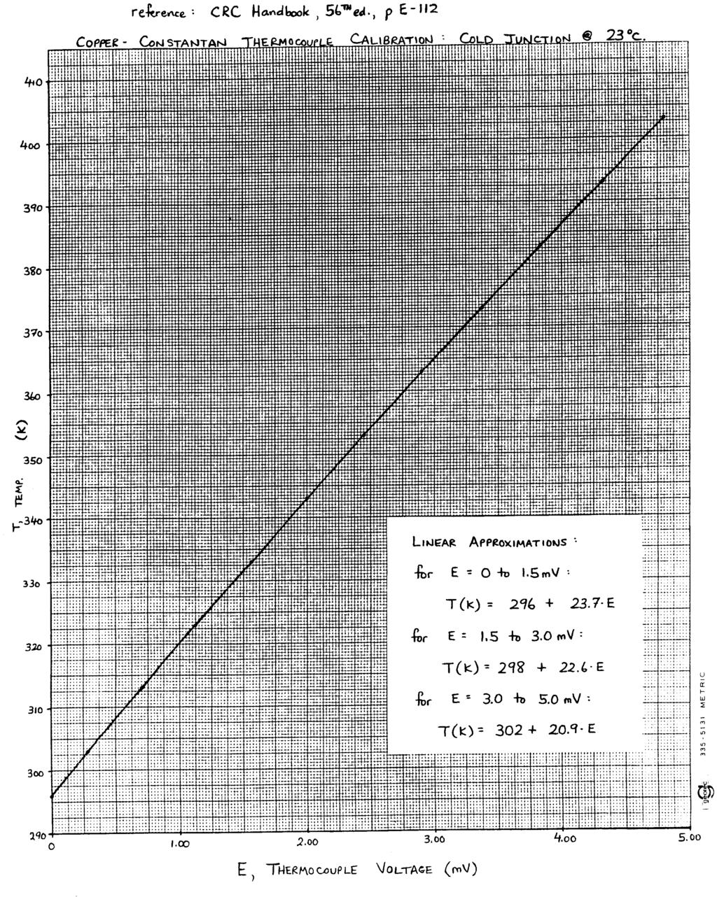
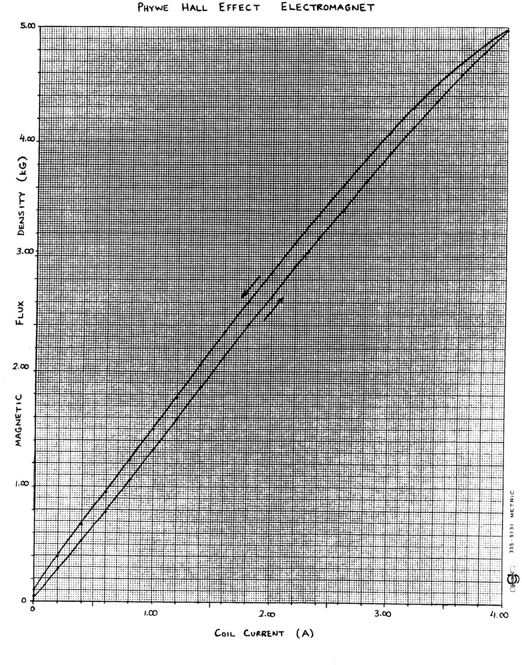
9 5 Feb 14 Semi.9 Apparatus Two samples are provided: one of p-type germanium and one of n-type germanium. The impurity levels in each sample are such that at room temperature they behave as extrinsic semiconductors (conduction due to charge carriers produced by impurity atoms, conductivity depends on impurity concentration and decreases with increasing temperature as per equations (15) and (16)). At temperatures greater than about 340 K (67 C) the samples behave as intrinsic semiconductors (conduction due to thermally-generated electron-hole pairs, conductivity increases with increasing temperature as per equation (14)). Each crystal (with dimensions 20 mm 10 mm 1 mm) is mounted on a supporting plate containing the necessary connections to the crystal as well as some additional components. The applied voltage, V x, is connected across terminals 2.1 and 2.3. Between terminals 2.2 and 2.3 is a current stabilizer/limiter. The voltage drop across the crystal is measured between terminals 2.1 and 2.2. Terminals 3 allow measurement of the Hall voltage. Adjusting control 5 allows compensation of interfering voltages that may be superimposed on the Hall voltage. i.e. When the magnetic field is 0, control 5 is adjusted to give 0 Hall voltage. Terminals 4 allow connection to the heating grid. A copper-constantan thermocouple connected to the crystal allows temperature measurement by measuring the thermoelectric voltage developed across terminals 7. Refer to the included graph and equations for the conversion between thermocouple voltage, V T, and absolute temperature. The magnetic field for the Hall effect measurements is provided by a pair of coils and a solid iron core. The calibration curve of magnetic field B z as a function of coil current I m is included. Figure 3
 and ask the instructor to confirm that the equipment is ready for use.")
10 5 Feb 14 Semi.10 Procedure and Experiment Figure 4 Check that the circuits are connected as shown in the circuit diagram (Figure 3) and ask the instructor to confirm that the equipment is ready for use. Turn on the meters to the appropriate settings, check that the heater circuit rheostat knob is fully CCW and turn on the power supply. 1. TEMPERATURE DEPENDENCE OF CONDUCTIVITY OF N-GE SAMPLE Check that the n-ge sample is connected and that it is raised out of the magnet. Adjust the 560 potentiometer fully clockwise until the current through the sample reaches its constant control value of about 25 ma. Turn on the heating coil current by turning the 5 rheostat fully clockwise. As soon as the thermocouple voltage reaches 5.0 mv back off the rheostat (turn it slightly counterclockwise) until the thermocouple voltage stops increasing. Do not allow the voltage reading to exceed 5.4 mv. Measure the voltage, V x, along the sample as a function of thermocouple voltage, V T. Take readings of V x at 0.2 mv intervals of V T for values of V T from 5.0 to 0.0 mv. Because of the relative insensitivity of the thermocouple voltmeter, the following procedure will be used to record the V x values: Take a V x reading when the thermocouple voltage has
11 5 Feb 14 Semi.11 just changed to the desired value, and again when the thermocouple voltage has just changed from the desired value. For example take the reading of V x when thermocouple voltage has just changed from 5.1 to 5.0 mv and again when thermocouple voltage has just changed from 5.0 to 4.9 mv. The value of V x corresponding to a thermocouple voltage of 5.0 mv is then the average of these two readings. 2. ROOM TEMPERATURE CONDUCTIVITY OF N-GE SAMPLE Set the control current at 4.0 ma by adjusting the 560 potentiometer. Record the value of applied voltage, V x. as a function of applied control current in 4 ma intervals from 4 ma to 24 ma. After completing the measurements, reduce the control current to 0 via the 560 potentiometer and disconnect the lead in the 15V terminal of the power supply. Ask the instructor to change the sample. 3. ROOM TEMPERATURE CONDUCTIVITY AND HALL EFFECT OF P-GE SAMPLE Plug in the magnet coil circuit and after demagnetizing the electromagnet by working down from 4.0 A in 0.5 A intervals, set the magnet current at 2.3 A (giving a magnetic flux density of 3.04 kg or T). Set the control current at 4.0 ma by adjusting the 560 potentiometer. With the sample raised out of the field, adjust the compensation control so that the Hall voltage meter reads 0. Record the value of applied voltage, V x. CAREFULLY move the sample down into the centre of the magnetic field and measure the Hall voltage. DO NOT FORCE THE SAMPLE BETWEEN THE POLE FACES. (The pole face gap is only slightly larger than the sample thickness.) Using the above procedure measure the applied voltage, V x, (when sample is out of field) and Hall voltage, V H, (when sample is in field) as a function of applied control current in 4 ma intervals from 4 ma to 24 ma. At each setting of control current the sample must be raised from the field, the applied voltage read, the compensation control adjusted to read 0 for Hall voltage, the sample lowered into the field, and the Hall voltage read. Examine the connections of the voltmeter used to measure the Hall voltage and determine the polarity of the Hall voltage (i.e. is the top of the sample positive or negative relative to the bottom of the sample?). Knowing the direction of the current (left to right when facing sample), the direction of the magnetic field ( out of the sample), and the polarity of the Hall voltage, determine the polarity of the majority charge carriers (refer to the discussion concerning the effect on the charge carriers motion of there being an applied magnetic field). 4. DEPENDENCE OF HALL VOLTAGE MAGNITUDE ON MAGNETIC FIELD - P-GE SAMPLE Reduce the magnetic field to 0 by reducing the magnet current. Adjust the 560 potentiometer until the control current is at its maximum value (about 25 ma). With the sample raised out of the magnetic field, adjust the compensation control to read 0 for Hall
12 5 Feb 14 Semi.12 voltage. Lower the sample into the magnetic field, and for magnet current values from 0.5 to 2.5 A in 0.5 A intervals, record the Hall voltage. 5. Perform procedure 1, TEMPERATURE DEPENDENCE OF CONDUCTIVITY, for the p-ge sample. Analysis: To avoid unit problems, use SI units (meters, kilograms, seconds, Volts, Amps, Tesla,...) throughout the calculations. The thermocouple calibration curve and/or calibration equations can be used to determine sample temperature in Kelvin at each data point. The results are: Thermo-couple Voltage, V T (mv) Sample Temp, T (K) 1/T (10 3 /K) ln(t)
13 5 Feb 14 Semi TEMPERATURE DEPENDENCE OF CONDUCTIVITY Plot ln(1/v x ) vs. 1/T. From the high temperature (intrinsic) portion of the curve determine a value for the energy gap of germanium (see equation (14) and recall that is directly proportional to 1/V x ). (Boltzmann s constant is k = ev/k.) The accepted value for E GAP for germanium is 0.67 ev. Plot ln(1/v x ) vs. ln(t) for the first 8 or so low temperature (extrinsic) points. Compare the slope of this linear, low temperature portion of the curve with the value predicted from equation (15) or equation (16) depending on which sample's data are being plotted. Recall that 1/V x is proportional to conductivity which in turn is directly dependent on charge carrier mobility. ROOM TEMPERATURE CONDUCTIVITY AND HALL EFFECT Plot the applied voltage vs. control current characteristic (V x vs. I c ) for each sample and from the slope and the sample dimensions determine the conductivity. Recall Ohm's Law, V = IR, and = 1/ = /RA, so the slope of V x vs. I c is R = / A. Thus the conductivity is given by ( slope) A Plot Hall voltage as a function of control current for constant magnetic field for the p-ge sample. Noting from equation (18) that the slope of this graph is R B H z, determine the Hall t coefficient. From the p-ge sample conductivity and the Hall coefficient determined above, determine the charge carrier concentration and the charge mobility (equations (21) and (8)). The hole mobility for pure germanium is m 2 /V s. DEPENDENCE OF HALL VOLTAGE MAGNITUDE ON MAGNETIC FIELD Using the magnet calibration curve and the Hall voltage versus magnet current data obtained for the p-ge sample, plot magnetic field versus Hall voltage. What is the significance of the shape of this plot?
14 5 Feb 14 Semi.14 ANALYSIS SPREADSHEET An Excel spreadsheet is available for use in tabulating the data, performing the required calculations, and producing the required graphs. The spreadsheet is obtained from the lab manual web page: Enter your data in the Data sheet. The data is automatically transferred to the Sample 1 and Sample 2 sheets, which are formatted for printing. These sheets also contain the results of most of the calculations that are required. The required graphs are automatically produced and can be viewed by selecting a sheet with a tab labelled Chart x.x. References: Experimental Physics, R.A. Dunlap, 1988, Oxford University Press, QC 33.D86 Introduction to Semiconductor Physics, Adler, Smith, & Longini, 1964, John Wiley & Sons, QC 612.S4A23 CRC Handbook of Chemistry and Physics, 56th Ed., CRC Press Principles of Electronic Instrumentation, Diefenderfer, 1972, W.B. Saunders Company Laboratory Physics, Meiners, Eppenstein, & Moore, 1969, John Wiley & Sons Experiments in Modern Physics, Melissinos, 1966, Academic Press, QC 33.M52 Semiconductors, Smith, 1959, Cambridge University Press, QC 612.S4S65
15
16
ADVANCED UNDERGRADUATE LABORATORY EXPERIMENT 20. Semiconductor Resistance, Band Gap, and Hall Effect
 ADVANCED UNDERGRADUATE LABORATORY EXPERIMENT 20 Semiconductor Resistance, Band Gap, and Hall Effect Revised: November 1996 by David Bailey March 1990 by John Pitre & Taek-Soon Yoon Introduction Solid materials
HALL EFFECT IN SEMICONDUCTORS
 Warsaw University of Technology Faculty of Physics Physics Laboratory I P Andrzej Kubiaczyk 30 HALL EFFECT IN SEMICONDUCTORS 1. ackground 1.1. Electron motion in electric and magnetic fields A particle
Last Revision: August,
 A3-1 HALL EFFECT Last Revision: August, 21 2007 QUESTION TO BE INVESTIGATED How to individual charge carriers behave in an external magnetic field that is perpendicular to their motion? INTRODUCTION The
Experiment 11: Hall Effect & Energy Gap in Germanium
 Experiment 11: Hall Effect & Energy Gap in Germanium We will see if the charge carrying particles are negative in n-doped germanium, and if they are positive in p-doped germanium. We will also measure
Hall effect in germanium
 Hall effect in germanium Principle The resistance and Hall voltage are measured on rectangular pieces of germanium as a function of the doping of the crystal, temperature and of magnetic field. From the
CLASS 12th. Semiconductors
 CLASS 12th Semiconductors 01. Distinction Between Metals, Insulators and Semi-Conductors Metals are good conductors of electricity, insulators do not conduct electricity, while the semiconductors have
n i exp E g 2kT lnn i E g 2kT
 HOMEWORK #10 12.19 For intrinsic semiconductors, the intrinsic carrier concentration n i depends on temperature as follows: n i exp E g 2kT (28.35a) or taking natural logarithms, lnn i E g 2kT (12.35b)
EXTRINSIC SEMICONDUCTOR
 EXTRINSIC SEMICONDUCTOR EXTRINSIC SEMICONDUCTOR A semiconductor in which the impurity atoms are added by doping process is called Extrinsic semiconductor. The addition of impurities increases the carrier
Electrical Resistance
 Electrical Resistance I + V _ W Material with resistivity ρ t L Resistance R V I = L ρ Wt (Unit: ohms) where ρ is the electrical resistivity 1 Adding parts/billion to parts/thousand of dopants to pure
Physical Structure of Matter Hall effect in p-germanium with Cobra3. Solid-state Physics, Plasma Physics.
 Physical Structure of Matter Solid-state Physics, Plasma Physics Hall effect in p-germanium with Cobra3 What you can learn about Semiconductor Band theory Forbidden zone Intrinsic conductivity Extrinsic
Unit III Free Electron Theory Engineering Physics
 . Introduction The electron theory of metals aims to explain the structure and properties of solids through their electronic structure. The electron theory is applicable to all solids i.e., both metals
Note that it is traditional to draw the diagram for semiconductors rotated 90 degrees, i.e. the version on the right above.
 5 Semiconductors The nearly free electron model applies equally in the case where the Fermi level lies within a small band gap (semiconductors), as it does when the Fermi level lies within a band (metal)
Introduction to Engineering Materials ENGR2000. Dr.Coates
 Introduction to Engineering Materials ENGR2000 Chapter 18: Electrical Properties Dr.Coates 18.2 Ohm s Law V = IR where R is the resistance of the material, V is the voltage and I is the current. l R A
Ch. 2: Energy Bands And Charge Carriers In Semiconductors
 Ch. 2: Energy Bands And Charge Carriers In Semiconductors Discrete energy levels arise from balance of attraction force between electrons and nucleus and repulsion force between electrons each electron
Electro - Principles I
 Electro - Principles I Page 10-1 Atomic Theory It is necessary to know what goes on at the atomic level of a semiconductor so the characteristics of the semiconductor can be understood. In many cases a
Due to the quantum nature of electrons, one energy state can be occupied only by one electron.
 In crystalline solids, not all values of the electron energy are possible. The allowed intervals of energy are called allowed bands (shown as blue and chess-board blue). The forbidden intervals are called
UMEÅ UNIVERSITY Department of Physics Agnieszka Iwasiewicz Leif Hassmyr Ludvig Edman SOLID STATE PHYSICS HALL EFFECT
 UMEÅ UNIVERSITY Department of Physics 2004-04-06 Agnieszka Iwasiewicz Leif Hassmyr Ludvig Edman SOLID STATE PHYSICS HALL EFFECT 1. THE TASK To measure the electrical conductivity and the Hall voltage for
ESE 372 / Spring 2013 / Lecture 5 Metal Oxide Semiconductor Field Effect Transistor
 Metal Oxide Semiconductor Field Effect Transistor V G V G 1 Metal Oxide Semiconductor Field Effect Transistor We will need to understand how this current flows through Si What is electric current? 2 Back
Physical Structure of Matter. Hall effect in p-germanium Solid-state Physics, Plasma Physics. What you need:
 Solid-state Physics, Plasma Physics Physical Structure of Matter What you can learn about Semiconductor Band theory Forbidden zone Intrinsic conductivity Extrinsic conductivity Valence band Conduction
ISSUES TO ADDRESS...
 Chapter 12: Electrical Properties School of Mechanical Engineering Choi, Hae-Jin Materials Science - Prof. Choi, Hae-Jin Chapter 12-1 ISSUES TO ADDRESS... How are electrical conductance and resistance
The Semiconductor in Equilibrium
 Lecture 6 Semiconductor physics IV The Semiconductor in Equilibrium Equilibrium, or thermal equilibrium No external forces such as voltages, electric fields. Magnetic fields, or temperature gradients are
HALL. Semiconductor Resistance, Band Gap, and Hall Effect
 ADVANCED UNDERGRADUATE LABORATORY HALL Semiconductor Resistance, Band Gap, and Hall Effect Revisions: September 2016, January 2018: Young-June Kim November 2011, January 2016: David Bailey October 2010:
ECE 250 Electronic Devices 1. Electronic Device Modeling
 ECE 250 Electronic Devices 1 ECE 250 Electronic Device Modeling ECE 250 Electronic Devices 2 Introduction to Semiconductor Physics You should really take a semiconductor device physics course. We can only
Lecture (02) Introduction to Electronics II, PN Junction and Diodes I
 Introduction to Electronics II, PN Junction and Diodes I") Lecture (02) Introduction to Electronics II, PN Junction and Diodes I By: Dr. Ahmed ElShafee ١ Agenda Current in semiconductors/conductors N type, P type semiconductors N Type Semiconductor P Type Semiconductor
Lecture (02) Introduction to Electronics II, PN Junction and Diodes I By: Dr. Ahmed ElShafee ١ Agenda Current in semiconductors/conductors N type, P type semiconductors N Type Semiconductor P Type Semiconductor
12/10/09. Chapter 18: Electrical Properties. View of an Integrated Circuit. Electrical Conduction ISSUES TO ADDRESS...
 Chapter 18: Electrical Properties ISSUES TO ADDRESS... How are electrical conductance and resistance characterized? What are the physical phenomena that distinguish? For metals, how is affected by and
EE 346: Semiconductor Devices
 EE 346: Semiconductor Devices Lecture - 6 02/06/2017 Tewodros A. Zewde 1 DENSTY OF STATES FUNCTON Since current is due to the flow of charge, an important step in the process is to determine the number
Calculating Band Structure
 Calculating Band Structure Nearly free electron Assume plane wave solution for electrons Weak potential V(x) Brillouin zone edge Tight binding method Electrons in local atomic states (bound states) Interatomic
Electrical Properties
 Electrical Properties Electrical Conduction R Ohm s law V = IR I l Area, A V where I is current (Ampere), V is voltage (Volts) and R is the resistance (Ohms or ) of the conductor Resistivity Resistivity,
CME 300 Properties of Materials. ANSWERS: Homework 9 November 26, As atoms approach each other in the solid state the quantized energy states:
 CME 300 Properties of Materials ANSWERS: Homework 9 November 26, 2011 As atoms approach each other in the solid state the quantized energy states: are split. This splitting is associated with the wave
Semiconductor Physics. Lecture 3
 Semiconductor Physics Lecture 3 Intrinsic carrier density Intrinsic carrier density Law of mass action Valid also if we add an impurity which either donates extra electrons or holes the number of carriers
FREQUENTLY ASKED QUESTIONS February 21, 2017
 FREQUENTLY ASKED QUESTIONS February 21, 2017 Content Questions How do you place a single arsenic atom with the ratio 1 in 100 million? Sounds difficult to get evenly spread throughout. Yes, techniques
Lecture 2 Electrons and Holes in Semiconductors
 EE 471: Transport Phenomena in Solid State Devices Spring 2018 Lecture 2 Electrons and Holes in Semiconductors Bryan Ackland Department of Electrical and Computer Engineering Stevens Institute of Technology
First-Hand Investigation: Modeling of Semiconductors
 perform an investigation to model the behaviour of semiconductors, including the creation of a hole or positive charge on the atom that has lost the electron and the movement of electrons and holes in
Electronic Devices & Circuits
 Electronic Devices & Circuits For Electronics & Communication Engineering By www.thegateacademy.com Syllabus Syllabus for Electronic Devices Energy Bands in Intrinsic and Extrinsic Silicon, Carrier Transport,
Mat E 272 Lecture 25: Electrical properties of materials
 Mat E 272 Lecture 25: Electrical properties of materials December 6, 2001 Introduction: Calcium and copper are both metals; Ca has a valence of +2 (2 electrons per atom) while Cu has a valence of +1 (1
Semiconductor Physics
 Semiconductor Physics Motivation Is it possible that there might be current flowing in a conductor (or a semiconductor) even when there is no potential difference supplied across its ends? Look at the
n N D n p = n i p N A
 Summary of electron and hole concentration in semiconductors Intrinsic semiconductor: E G n kt i = pi = N e 2 0 Donor-doped semiconductor: n N D where N D is the concentration of donor impurity Acceptor-doped
EE301 Electronics I , Fall
 EE301 Electronics I 2018-2019, Fall 1. Introduction to Microelectronics (1 Week/3 Hrs.) Introduction, Historical Background, Basic Consepts 2. Rewiev of Semiconductors (1 Week/3 Hrs.) Semiconductor materials
Semiconductor Physics and Devices Chapter 3.
 Introduction to the Quantum Theory of Solids We applied quantum mechanics and Schrödinger s equation to determine the behavior of electrons in a potential. Important findings Semiconductor Physics and
Microscopic Ohm s Law
 Microscopic Ohm s Law Outline Semiconductor Review Electron Scattering and Effective Mass Microscopic Derivation of Ohm s Law 1 TRUE / FALSE 1. Judging from the filled bands, material A is an insulator.
CLASS 1 & 2 REVISION ON SEMICONDUCTOR PHYSICS. Reference: Electronic Devices by Floyd
 CLASS 1 & 2 REVISION ON SEMICONDUCTOR PHYSICS Reference: Electronic Devices by Floyd 1 ELECTRONIC DEVICES Diodes, transistors and integrated circuits (IC) are typical devices in electronic circuits. All
Semiconductors 1. Explain different types of semiconductors in detail with necessary bond diagrams. Intrinsic semiconductors:
 Semiconductors 1. Explain different types of semiconductors in detail with necessary bond diagrams. There are two types of semi conductors. 1. Intrinsic semiconductors 2. Extrinsic semiconductors Intrinsic
EXTRINSIC SEMICONDUCTOR
 EXTRINSIC SEMICONDUCTOR In an extrinsic semiconducting material, the charge carriers originate from impurity atoms added to the original material is called impurity [or] extrinsic semiconductor. This Semiconductor
Atoms? All matters on earth made of atoms (made up of elements or combination of elements).
.") Chapter 1 Atoms? All matters on earth made of atoms (made up of elements or combination of elements). Atomic Structure Atom is the smallest particle of an element that can exist in a stable or independent
Chapter 1 Atoms? All matters on earth made of atoms (made up of elements or combination of elements). Atomic Structure Atom is the smallest particle of an element that can exist in a stable or independent
Lecture 2. Semiconductor Physics. Sunday 4/10/2015 Semiconductor Physics 1-1
 Lecture 2 Semiconductor Physics Sunday 4/10/2015 Semiconductor Physics 1-1 Outline Intrinsic bond model: electrons and holes Charge carrier generation and recombination Intrinsic semiconductor Doping:
TALLINN UNIVERSITY OF TECHNOLOGY, INSTITUTE OF PHYSICS 6. THE TEMPERATURE DEPENDANCE OF RESISTANCE
 6. THE TEMPERATURE DEPENDANCE OF RESISTANCE 1. Objective Determining temperature coefficient of metal and activation energy of self-conductance of semiconductor sample. 2. Equipment needed Metal and semiconductor
Concept of Core IENGINEERS- CONSULTANTS LECTURE NOTES SERIES ELECTRONICS ENGINEERING 1 YEAR UPTU. Page 1
 Concept of Core Conductivity of conductor and semiconductor can also be explained by concept of Core. Core: Core is a part of an atom other than its valence electrons. Core consists of all inner shells
Variation of Energy Bands with Alloy Composition E
 Variation of Energy Bands with Alloy Composition E 3.0 E.8.6 L 0.3eV Al x GaAs AlAs 1- xas 1.43eV.16eV X k.4 L. X.0 X 1.8 L 1.6 1.4 0 0. 0.4 0.6 X 0.8 1 1 Carriers in intrinsic Semiconductors Ec 4º 1º
Higher Physics. Electricity. Summary Notes. Monitoring and measuring a.c. Current, potential difference, power and resistance
 Higher Physics Electricity Summary Notes Monitoring and measuring a.c. Current, potential difference, power and resistance Electrical sources and internal resistance Capacitors Conductors, semiconductors
Physical structure of matter Band gap of germanium with Cobra3. Solid-state Physics, Plasma Physics. What you need:
 Physical structure of matter Solid-state Physics, Plasma Physics Band gap of germanium with Cobra3 What you can learn about Semiconductor Band theory Forbidden band Intrinsic conduction Extrinsic conduction
Assumptions of classical free electron model
 Module 2 Electrical Conductivity in metals & Semiconductor 1) Drift Velocity :- The Velocity attain by an Electron in the Presence of applied electronic filed is Known as drift Velocity. 2) Mean free Path:-
Lecture 1. OUTLINE Basic Semiconductor Physics. Reading: Chapter 2.1. Semiconductors Intrinsic (undoped) silicon Doping Carrier concentrations
 silicon Doping Carrier concentrations") Lecture 1 OUTLINE Basic Semiconductor Physics Semiconductors Intrinsic (undoped) silicon Doping Carrier concentrations Reading: Chapter 2.1 EE105 Fall 2007 Lecture 1, Slide 1 What is a Semiconductor? Low
Lecture 1 OUTLINE Basic Semiconductor Physics Semiconductors Intrinsic (undoped) silicon Doping Carrier concentrations Reading: Chapter 2.1 EE105 Fall 2007 Lecture 1, Slide 1 What is a Semiconductor? Low
EE 446/646 Photovoltaic Devices I. Y. Baghzouz
 EE 446/646 Photovoltaic Devices I Y. Baghzouz What is Photovoltaics? First used in about 1890, the word has two parts: photo, derived from the Greek word for light, volt, relating to electricity pioneer
Unit IV Semiconductors Engineering Physics
 Introduction A semiconductor is a material that has a resistivity lies between that of a conductor and an insulator. The conductivity of a semiconductor material can be varied under an external electrical
3. Consider a semiconductor. The concentration of electrons, n, in the conduction band is given by
 Colloqium problems to chapter 13 1. What is meant by an intrinsic semiconductor? n = p All the electrons are originating from thermal excitation from the valence band for an intrinsic semiconductor. Then
Bohr s Model, Energy Bands, Electrons and Holes
 Dual Character of Material Particles Experimental physics before 1900 demonstrated that most of the physical phenomena can be explained by Newton's equation of motion of material particles or bodies and
Carrier Mobility and Hall Effect. Prof.P. Ravindran, Department of Physics, Central University of Tamil Nadu, India
 Carrier Mobility and Hall Effect 1 Prof.P. Ravindran, Department of Physics, Central University of Tamil Nadu, India http://folk.uio.no/ravi/semi2013 calculation Calculate the hole and electron densities
ELECTRONIC I Lecture 1 Introduction to semiconductor. By Asst. Prof Dr. Jassim K. Hmood
 ELECTRONIC I Lecture 1 Introduction to semiconductor By Asst. Prof Dr. Jassim K. Hmood SOLID-STATE ELECTRONIC MATERIALS Electronic materials generally can be divided into three categories: insulators,
Lab 4: The Classical Hall Effect
 Lab 4: The Classical Hall Effect Background A particle with charge q moving with a velocity v in a uniform magnetic field B will experience a force F, F = q( v B ) (1) 1 Introduction Understanding the
Free Electron Model for Metals
 Free Electron Model for Metals Metals are very good at conducting both heat and electricity. A lattice of in a sea of electrons shared between all nuclei (moving freely between them): This is referred
Density of states for electrons and holes. Distribution function. Conduction and valence bands
 Intrinsic Semiconductors In the field of semiconductors electrons and holes are usually referred to as free carriers, or simply carriers, because it is these particles which are responsible for carrying
Lecture (02) PN Junctions and Diodes
 PN Junctions and Diodes") Lecture (02) PN Junctions and Diodes By: Dr. Ahmed ElShafee ١ I Agenda N type, P type semiconductors N Type Semiconductor P Type Semiconductor PN junction Energy Diagrams of the PN Junction and Depletion
Lecture (02) PN Junctions and Diodes By: Dr. Ahmed ElShafee ١ I Agenda N type, P type semiconductors N Type Semiconductor P Type Semiconductor PN junction Energy Diagrams of the PN Junction and Depletion
A semiconductor is an almost insulating material, in which by contamination (doping) positive or negative charge carriers can be introduced.
 positive or negative charge carriers can be introduced.") Semiconductor A semiconductor is an almost insulating material, in which by contamination (doping) positive or negative charge carriers can be introduced. Page 2 Semiconductor materials Page 3 Energy levels
Semiconductor A semiconductor is an almost insulating material, in which by contamination (doping) positive or negative charge carriers can be introduced. Page 2 Semiconductor materials Page 3 Energy levels
3C3 Analogue Circuits
 Department of Electronic & Electrical Engineering Trinity College Dublin, 2014 3C3 Analogue Circuits Prof J K Vij jvij@tcd.ie Lecture 1: Introduction/ Semiconductors & Doping 1 Course Outline (subject
Experiment The Hall Effect Physics 2150 Experiment No. 12 University of Colorado
 Experiment 12 1 Introduction The Hall Effect Physics 2150 Experiment No. 12 University of Colorado The Hall Effect can be used to illustrate the effect of a magnetic field on a moving charge to investigate
Chapter Two. Energy Bands and Effective Mass
 Chapter Two Energy Bands and Effective Mass Energy Bands Formation At Low Temperature At Room Temperature Valence Band Insulators Metals Effective Mass Energy-Momentum Diagrams Direct and Indirect Semiconduction
KATIHAL FİZİĞİ MNT-510
 KATIHAL FİZİĞİ MNT-510 YARIİLETKENLER Kaynaklar: Katıhal Fiziği, Prof. Dr. Mustafa Dikici, Seçkin Yayıncılık Katıhal Fiziği, Şakir Aydoğan, Nobel Yayıncılık, Physics for Computer Science Students: With
Lecture 7: Extrinsic semiconductors - Fermi level
 Lecture 7: Extrinsic semiconductors - Fermi level Contents 1 Dopant materials 1 2 E F in extrinsic semiconductors 5 3 Temperature dependence of carrier concentration 6 3.1 Low temperature regime (T < T
collisions of electrons. In semiconductor, in certain temperature ranges the conductivity increases rapidly by increasing temperature
 1.9. Temperature Dependence of Semiconductor Conductivity Such dependence is one most important in semiconductor. In metals, Conductivity decreases by increasing temperature due to greater frequency of
Conductivity and Semi-Conductors
 Conductivity and Semi-Conductors J = current density = I/A E = Electric field intensity = V/l where l is the distance between two points Metals: Semiconductors: Many Polymers and Glasses 1 Electrical Conduction
Hall Coefficient of Germanium
 Sridhar Chandramouli 1 Hall Coefficient of Germanium Physics Department, The College of Wooster, Wooster, Ohio 691 April 9, 1999 This experiment experimentally measures the Hall coefficient of a Germanium
After successfully completing this laboratory assignment, including the assigned reading, the lab
 University of California at Santa Cruz Jack Baskin School of Engineering Electrical Engineering Department EE-145L: Properties of Materials Laboratory Lab 6: Temperature Dependence of Semiconductor Conductivity
Doped Semiconductors *
 OpenStax-CNX module: m1002 1 Doped Semiconductors * Bill Wilson This work is produced by OpenStax-CNX and licensed under the Creative Commons Attribution License 1.0 To see how we can make silicon a useful
DO PHYSICS ONLINE ELECTRIC CURRENT FROM IDEAS TO IMPLEMENTATION ATOMS TO TRANSISTORS ELECTRICAL PROPERTIES OF SOLIDS
 DO PHYSICS ONLINE FROM IDEAS TO IMPLEMENTATION 9.4.3 ATOMS TO TRANSISTORS ELECTRICAL PROPERTIES OF SOLIDS ELECTRIC CURRENT Different substances vary considerably in their electrical properties. It is a
CHAPTER 2: ENERGY BANDS & CARRIER CONCENTRATION IN THERMAL EQUILIBRIUM. M.N.A. Halif & S.N. Sabki
 CHAPTER 2: ENERGY BANDS & CARRIER CONCENTRATION IN THERMAL EQUILIBRIUM OUTLINE 2.1 INTRODUCTION: 2.1.1 Semiconductor Materials 2.1.2 Basic Crystal Structure 2.1.3 Basic Crystal Growth technique 2.1.4 Valence
Observation of the Hall Effect, and measurement of the Hall constant of a few semi-conductors and metals samples.
 H6-1 H6. Hall Effect I. OBJECTIVE OF THE EXPERIMENT Observation of the Hall Effect, and measurement of the Hall constant of a few semi-conductors and metals samples. II THEORETICAL BACKGROUND When a current
Free Electron Model for Metals
 Free Electron Model for Metals Metals are very good at conducting both heat and electricity. A lattice of in a sea of electrons shared between all nuclei (moving freely between them): This is referred
Semiconductor Devices and Circuits Fall Midterm Exam. Instructor: Dr. Dietmar Knipp, Professor of Electrical Engineering. Name: Mat. -Nr.
 Semiconductor Devices and Circuits Fall 2003 Midterm Exam Instructor: Dr. Dietmar Knipp, Professor of Electrical Engineering Name: Mat. -Nr.: Guidelines: Duration of the Midterm: 1 hour The exam is a closed
Practical 1P4 Energy Levels and Band Gaps
 Practical 1P4 Energy Levels and Band Gaps What you should learn from this practical Science This practical illustrates some of the points from the lecture course on Elementary Quantum Mechanics and Bonding
Engineering 2000 Chapter 8 Semiconductors. ENG2000: R.I. Hornsey Semi: 1
 Engineering 2000 Chapter 8 Semiconductors ENG2000: R.I. Hornsey Semi: 1 Overview We need to know the electrical properties of Si To do this, we must also draw on some of the physical properties and we
ECE 335: Electronic Engineering Lecture 2: Semiconductors
 Faculty of Engineering ECE 335: Electronic Engineering Lecture 2: Semiconductors Agenda Intrinsic Semiconductors Extrinsic Semiconductors N-type P-type Carrier Transport Drift Diffusion Semiconductors
UNIT - IV SEMICONDUCTORS AND MAGNETIC MATERIALS
 1. What is intrinsic If a semiconductor is sufficiently pure, then it is known as intrinsic semiconductor. ex:: pure Ge, pure Si 2. Mention the expression for intrinsic carrier concentration of intrinsic
Carriers Concentration, Current & Hall Effect in Semiconductors. Prof.P. Ravindran, Department of Physics, Central University of Tamil Nadu, India
 Carriers Concentration, Current & Hall Effect in Semiconductors 1 Prof.P. Ravindran, Department of Physics, Central University of Tamil Nadu, India http://folk.uio.no/ravi/semi2013 Conductivity Charge
Practical 1P4 Energy Levels and Band Gaps
 Practical 1P4 Energy Levels and Band Gaps What you should learn from this practical Science This practical illustrates some of the points from the lecture course on Elementary Quantum Mechanics and Bonding
Fundamentals of Semiconductor Devices Prof. Digbijoy N. Nath Centre for Nano Science and Engineering Indian Institute of Science, Bangalore
 Fundamentals of Semiconductor Devices Prof. Digbijoy N. Nath Centre for Nano Science and Engineering Indian Institute of Science, Bangalore Lecture - 05 Density of states Welcome back. So, today is the
EECS130 Integrated Circuit Devices
 EECS130 Integrated Circuit Devices Professor Ali Javey 8/30/2007 Semiconductor Fundamentals Lecture 2 Read: Chapters 1 and 2 Last Lecture: Energy Band Diagram Conduction band E c E g Band gap E v Valence
This lab was adapted from Kwantlen University College s Determination of e/m lab.
 e /m: Charge to Mass Ratio of the Electron This lab was adapted from Kwantlen University College s Determination of e/m lab. Purpose To determine the charge to mass ratio of the electron, e /m, using Helmholtz
From Last Time Important new Quantum Mechanical Concepts. Atoms and Molecules. Today. Symmetry. Simple molecules.
 Today From Last Time Important new Quantum Mechanical Concepts Indistinguishability: Symmetries of the wavefunction: Symmetric and Antisymmetric Pauli exclusion principle: only one fermion per state Spin
BETA-RAY SPECTROMETER
 14 Sep 07 β-ray.1 BETA-RAY SPECTROMETER In this experiment, a 180, constant-radius magnetic spectrometer consisting of an electromagnet with a Geiger-Muller detector, will be used to detect and analyze
MAGNETIC DEFLECTION. OBJECTIVE: To observe the effect of a magnetic field on an electron beam. To measure the Earth s magnetic field.
 MAGNETIC DEFLECTION OBJECTIVE: To observe the effect of a magnetic field on an electron beam. To measure the Earth s magnetic field. THEORY: Moving charges exert forces on one another that are not observed
Introduction to Semiconductor Physics. Prof.P. Ravindran, Department of Physics, Central University of Tamil Nadu, India
 Introduction to Semiconductor Physics 1 Prof.P. Ravindran, Department of Physics, Central University of Tamil Nadu, India http://folk.uio.no/ravi/cmp2013 Review of Semiconductor Physics Semiconductor fundamentals
Fall 2014 Nobby Kobayashi
 University of California at Santa Cruz Jack Baskin School of Engineering Electrical Engineering Department EE-145L: Properties of Materials Laboratory Lab 5: Temperature Dependence of Semiconductor Conductivity
Three Most Important Topics (MIT) Today
 Today") Three Most Important Topics (MIT) Today Electrons in periodic potential Energy gap nearly free electron Bloch Theorem Energy gap tight binding Chapter 1 1 Electrons in Periodic Potential We now know the
Three Most Important Topics (MIT) Today Electrons in periodic potential Energy gap nearly free electron Bloch Theorem Energy gap tight binding Chapter 1 1 Electrons in Periodic Potential We now know the
Charge Carriers in Semiconductor
 Charge Carriers in Semiconductor To understand PN junction s IV characteristics, it is important to understand charge carriers behavior in solids, how to modify carrier densities, and different mechanisms
ECE 142: Electronic Circuits Lecture 3: Semiconductors
 Faculty of Engineering ECE 142: Electronic Circuits Lecture 3: Semiconductors Agenda Intrinsic Semiconductors Extrinsic Semiconductors N-type P-type Carrier Transport Drift Diffusion Semiconductors A semiconductor
Crystal Properties. MS415 Lec. 2. High performance, high current. ZnO. GaN
 Crystal Properties Crystal Lattices: Periodic arrangement of atoms Repeated unit cells (solid-state) Stuffing atoms into unit cells Determine mechanical & electrical properties High performance, high current
Lecture 3: Electron statistics in a solid
 Lecture 3: Electron statistics in a solid Contents Density of states. DOS in a 3D uniform solid.................... 3.2 DOS for a 2D solid........................ 4.3 DOS for a D solid........................
Session 5: Solid State Physics. Charge Mobility Drift Diffusion Recombination-Generation
 Session 5: Solid State Physics Charge Mobility Drift Diffusion Recombination-Generation 1 Outline A B C D E F G H I J 2 Mobile Charge Carriers in Semiconductors Three primary types of carrier action occur
Electronics The basics of semiconductor physics
 Electronics The basics of semiconductor physics Prof. Márta Rencz, Gergely Nagy BME DED September 16, 2013 The basic properties of semiconductors Semiconductors conductance is between that of conductors
Chapter 1 Overview of Semiconductor Materials and Physics
 Chapter 1 Overview of Semiconductor Materials and Physics Professor Paul K. Chu Conductivity / Resistivity of Insulators, Semiconductors, and Conductors Semiconductor Elements Period II III IV V VI 2 B