ESE 570 MOS INVERTERS DYNAMIC CHARACTERISTICS. Kenneth R. Laker, University of Pennsylvania, updated 26Feb15
|
|
|
- Basil Stephens
- 6 years ago
- Views:
Transcription
1 ESE 570 MOS INVERTERS DYNAMIC CHARACTERISTICS 1
2 Usually Cdb >> Cgd & Csb >> Cgs extrinsic parasitic caps n = fan-out 1 # dbn Cload = C + #C# dbp +#C# gdn +#C# gdp +# C # int + ncgb Parasitic Caps updated 6Feb15 Kenneth Intrinsic R. Laker, University of Pennsylvania, # C# # + C dbp + Cint + n Cgb i i dbn Cgb = Cgbn+ Cgbp worst case
3 Cload Cdbn + Cdbp + Cint + ncgb where n = fan-out 1 3

4 t 0 0 V50% = / 4

5 0 0 V50% = / 5
6 0 V10% = 0.1 V90% = 0.9 6
7 MOS Inverter Dynamic Performance 1. ANALYSIS (OR SIMULATION): For a given MOS inverter schematic + Cload, estimate (or determine) the propagation delays τphl and/or τplh, OR the rise/fall times τrise and/or τfall.. DESIGN: For given specs for the propagation delays τphl and/or τplh, OR the rise/fall times τrise and/or τfall + Cload, determine the MOS inverter schematic. METHODS: 1. Average Current Model >PHL C load 8V HL 5V OH V 50%p 6 =C load I avg, HL I avg, HL. Differential Equation Model i C =C load d V out d V out dt=c load dt ic where dt > PHL 3. 1st Order RC Delay Model Assume Vin ideal >PHL 0.69 C load Rn 7
8 CALCULATION OF PROPOGATION DELAY TIMES C load 8V HL C load 5V DD V DD /6 > PHL = =C load R eff, HL I avg, HL I avg, HL C load 8V LH C load 5V DD / 06 > PLH = =C load R eff, LH I avg, LH I avg, LH t 0 0 0, t 0 0, /)] /)] 8
9 CALCULATION OF RISE & FALL TIMES 0 ( ) ( ) ic = idp - idn 0.1)] 0, 0, 0.9)] 9
10 Calculating Propagation Delays By Solving the Circuit Differential Equation Let's assume Vin is an ideal step-input. Two Cases 1. Vin abruptly rises => Vout falls => > PHL. Vin abruptly falls => Vout rises => > PLH idp - idn 10
11 1) Vin ABRUPTLY RISES CASE ->> PHL Vin(t = t0) = 0 -> Vin(t < t0) = 0 and Vout (t < t0) = LIN V50% Vout < - VT0n i Dp 0 V out =V DD V T0n C load d V out d V out i Dn dt =C load 5 6 dt i Dn V50%= / t sat 11

12 CMOS Static Inverter Characteristics Recall 1
13 1) Vin ABRUPTLY RISES CASE ->> PHL Vin(t = t0) = 0 -> V50%= / C load d V out d V out i Dn dt =C load 5 6 dt i Dn V out =0.5V DD t=t50% 50 > phl = t=t dt =C load V 0 out =V DD t sat 1 5 6dV out =C load Reff, HL i Dn 0.5V dV out 1C load V V 5 6 dv out i Dn i Dn tsat - t0 t50% - tsat V DD V T0n.=C load V DD nmos SAT DD DD T0n nmos LIN = t50% - t0 13
14 1) Vin ABRUPTLY RISES CASE => > PHL cont. t0 < t < tsat i = k n 5V V 6 = i Dn in T0n C kn dv out 5V in V T0n 6 = C load dt for Vin = and V DD V T0n V out V DD V50%= / dv out dv out => dt =C load i Dn= C load i Dn dt t sat tt'1sat V DD V T0n t dt =C load V 0 C load tt1sat ' t dt = k 0 n ' 1 sat t t 0 = DD 1 5 6dV out i Dn V DD V T0n 5V DD V T0n 6 V DD dv out C load V T0n k n 5V DD V T0n 6 14
15 1) Vin ABRUPTLY RISES CASE => > PHL cont. tsat < t < t50% kn i Dn= [5V in V T0n 6V out V out ]= i C kn dv out [5V DD V T0n 6V out V out ]= C load dt 0 V50%= / t50% 50p tt t sat ' 1 sat V50% 50p dt=c load V tsat DD V T0n 1 5 6dV out i Dn tsat V out V DD V T0n Vin = and Vout = V 0.5V 50% DD VT0n V = V- V out DD T0n 15
16 1) Vin ABRUPTLY RISES CASE => > PHL cont. Vout = V50% = 0.5 tsat tt t 0 = tsat / / ' 1 sat Vout = VDD- VT0n C load V T0n k n 5V DD V T0n 6 tsat / / / Rn 16
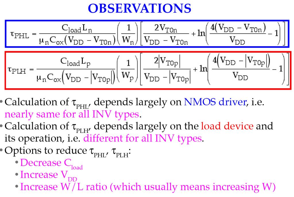
17 1) Vin ABRUPTLY RISES CASE > PHL => cont. / Recall from static CMOS Inverter: k n k 'n 5W / L6n =n 5W / L6n k R= = ' = k p k p 5W / L6 p = p 5W / L6 p DESIGN: (1) Vth kr; () τphl kn; (3) kr & kn kp 17
18 SOMETIMES USED APPROXIMATION FOR τphl C load tt=t =t'50% > PHL= t=t dt 1 0. kn 5V DD V T0n 6 V out =V DD dv out C load 50.5V DD 6 k n 5V DD V T0n 6 > PHL t sat V out =0.5 V DD C load V DD k n 5V DD V T0n 6 R n C load Δ is less than 10% 18
19 = 5 V, VGSn = 5 V and VDSn 4V => idn = idnsat = 5mA V V50% = 0.5 =.5 19
20 Example 6.1 cont. 1 pf V V.= [ 1ln 5 16] 3 5V 0.65 x 10 A/V 55 16V 55 16V 1 pf 16.= [ 1ln 5 16]=0.5 ns x 10 A/V UNITS: F F C /V = V= V =s A/V A C /s 0
21 COMPARISON WITH SOMETIMES USED APPROXIMATION FOR τphl = 0.5 ns Approximation for τphl 1 x 10 1 F 5V > PHL = =0.5 ns k n 5V DD V T0n 6 10 A 54 V 6 4V C load V DD where k n = i Dnsat 10 ma 3 = =0.65 x 10 A /V 5V DD V T0n 6 54 V 6 1
22 DD DD DD DD 0.99 ma A

23 Example 6. cont ns x 10 A DD tsat tsat -6.5 x s/v Vout Vout = 4.0V Vout = 4.5V tsat 0.31 ns 3
24 Example 6. cont ns tsat tsat Vin = 5 V 0.5 V tsat 0.5 V Vin = 5 V 3.39 ns tsat tsat 3.39 ns ns = 3.70 ns 4
25 ) Vin ABRUPTLY FALLS CASE => > PLH Vout (t < t0) = 0, Vin(t = t0) = -> 0 SAT 0 < Vout - VT0p LIN - VT0p < Vout / V50%= / i Dn 0 tsat C load d V out d V out i Dp dt =C load 5 6 dt i Dp 5

26 CMOS Static Inverter Characteristics Recall i Dn 0 6
27 ) Vin ABRUPTLY FALLS CASE => > PLH V50%= / C load tsat d V out d V out i Dp dt =C load 5 6 dt i Dp V out =V50% 50p t=t 50p 50% > PLH = t=t dt=c load V 0 V T0p.=C load out =0 5 1 i Dp 6dV out =C load R eff, LH V50% 50p 6 dv out 1C load V 5 i Dp tsat - t0 pmos SAT 1 6dV out = t - t 50% 0 i Dp t50% - tsat T0p pmos LIN 7

28 ) Vin ABRUPTLY FALLS CASE > PLH => cont. /. R p C load Recall from static CMOS Inverter: k n k 'n 5W / L6n =n 5W / L6n k R= = ' = k p k p 5W / L6 p = p 5W / L6 p DESIGN: (1) Vth kr; () τplh kp; (3) kr & kp kn 8
29 SOMETIMES USED APPROXIMATION FOR τplh C load t =t sat > PLH = t =t dt 0 kp 5V DD V T0p 6. V50%= / tsat > PLH V out =0.5 V DD V out =0 dv out C load 50.5V DD 6 k p 5V DD V T0p 6 C load V DD k p 5V DD V T0p 6 R p C load Δ is less than 10% 9
30 Inverter Dynamic Performance Quick Review 1. ANALYSIS (OR SIMULATION): For a given MOS inverter schematic + Cload, estimate (or determine) the propagation delays τphl and/or τplh, OR the rise/fall times τrise and/or τfall.. DESIGN: For given specs for the propagation delays τphl and/or τplh, OR the rise/fall times τrise and/or τfall + Cload, determine the MOS inverter schematic. METHODS: 1. Average Current Model >PHL C load 8V HL 5V OH V 50%p 6 =C load I avg, HL I avg, HL. Differential Equation Model d V out d V out i C =C load dt=c load dt ic st 3. 1 Order RC Delay Model >PHL 0.69 C load R n Assume Vin ideal 30
31 Quick Review τplh & τphl Differential Equation Model CONDITIONS for Balanced CMOS Propagation Delays, i.e. =n W W => 5 L 6 = = 5 L 6 p n p i.e. Symmetrical Inverter 31
32 µp 3
33 7 33
34 ALTERNATIVE APPROXIMATE DELAY DESIGN FORMULAS Using the approximate delay formulas on slides 18 and 9: > PHL C load V DD k n 5V DD V T0n 6 R n C load Wn k n ==n C ox Ln Wn C load V DD L n >PHL =n C ox 5V DD V T0n 6 > PLH C load V DD k p 5V DD V T0p 6 R p C load Wp k p == p C ox Lp Wp C load V DD L p > PLH = p C ox 5V DD V T0p 6 34
35 35

36 Example 6.3 cont. t 5V out =1V 6 V out =1V dv out dt= C load i 5lin6 Dn t 5V =4 V 6 out V out =4V
37 Example 6.3 cont Wn = 8.11 (1 µm) = 8.11 µm 8.11 µm = µm 37
38 µp 38
39 Design for Propagation Delays Using More Realistic Model for Cload Cload i i Cdbn + Cdbp + Cint + Cgb (Wn, Wp). Cload i i Cdbn(Wn) + Cdbp(Wp) + Cint + Cgb 39
40 Design for Propagation Delays Using More Realistic Model for Cload cont. Cdbn (Wn) = [Wn (Y + xj)] Cj0n Keqn + (Wn + Y) Cjswn Keqn(sw) Cdbp (Wp) = [Wp (Y + xj)] Cj0p Keqp + (Wp + Y) Cjswp Keqp(sw) Cload = α0 + αnwn + αpwp α0 = YCjswnKeqn + YCjswpKeqp + Cint + Cgb αn = (Y + xj)cj0nkeqn + CjswnKeqn αp = (Y + xj)cj0pkeqp + CjswpKeqp 40
41 Design for Propagation Delays Using More Realistic Model for Cload cont. µp C load > PHL =7 n Wn = α0 + (αn + (Wp/Wn) αp)wn C load > PLH =7 p and Wp where Cload = α0 + αnwn + αpwp Γn and ΓP are set largely by process parameters and V DD. const. 41
42 C load > PHL=7 n Wn Cload = α0 + αnwn + αpwp C load > PLH =7 p Wp Cload = α0 + αnwn + αpwp Multiply and divide αpwp by Wn Multiply and divide αnwn by Wp Cload = α0 + αnwn + (αpwp/wn)wn = α0 + [αn + αpr]wn Cload = α0 + (αnwn/wp)wp + αpwp = α0 + [αn/r + αp]wp where R = Wp/Wn = constant α0 + [αn + αpr]wn τphl? Γn Wn 1 =p W p (Recall: V th = when Lp=Ln) k R =n W n α0 + [αn/r + αp]wp τplh? Γp Wp 4
43 Design for Propagation Delays Using More Realistic Model for Cload cont. α0 + [αn/r + αp]wp α0 + [αn + αpr]wn τphl? Γn Wn τplh? Γp where R = aspect ratio = Wp/Wn Wp Hence increasing Wn and Wp will have diminishing influence on τphl and τplh as they become large, i.e. = > Limit PHL limit τphl = Γn [αn + αp R] Wn large R = constant = limit τplh = Γp [αn/r + αp] > Limit PLH Wp large R = constant absolute minimum delays α0 = f(cint, Cgb). P avg C load V DD f 43
44 Design for Propagation Delays Using More Realistic Model for Cload cont. = > Limit PHL limit τphl = Γn [αn + αp R] Wn large R = constant = limit τplh = Γp [αn/r + αp] > Limit PLH absolute minimum delays Wp large R = constant 44
45 Design for Propagation Delays Using More Realistic Model for Cload cont. 1.6 = 3.3 V External load cap = 100 ff R = Wp/Wn =.75 Ln = Lp = 0.8 µm 1.4 τphl (ns) Area x τphlproduct (norm) nmos Channel Width Wn (µm) minimum nmos Channel Width Wn (µm) 45
46 Taking Into Account Non-Ideal Input Waveform ideal Vin non-ideal Vin Vout to ideal Vin Vout to non-ideal Vin 46

 Capacitance directly proportional to gate width (W) Conductance directly proportional to gate width (W) Resistance is inversely")
47 st 1 Order RC DELAY MODELS Equivalent circuits used for MOS transistors Ideal switch + effective ON resistance + load capacitance. Unit nmos has effective ON resistance Rn= Run/κn & capacitance Cd. Unit pmos has effective ON resistance Rp = Rup/κp & capacitance κpcd; where transistor scale factors κn 1 and κp 1, i.e. Wn = κnwun, Wp = κpwup Cgb = Cg and Cdb = Csb = Cd for the unit n,pmos transistors and scale with κn, κp. NMOS and pmos transistor at minimum gate length (L) Capacitance directly proportional to gate width (W) Conductance directly proportional to gate width (W) Resistance is inversely proportional to gate width (W) Example Unit Transistors Example Unit Dimensions: L un=lup =< ; W un =W up =4 < 47
48 st 1 Order RC Elmore Delay Model > PLH Step Source 1 t 0 0 V 1 506=0 > PHL Step Source 1 t 0 0 > PLH > PHL V 1 506=V DD > PLH Rn or Rp V1(0) V1(t) Cload V 1 5t6=V DD 51 e t / R p C load 6 V DD > / R V50% = =V 51 e 50p DD V DD V50% 1 > / R C 50p e = = V DD PLH PLH p nu load > PLH =ln 56C load R p =0.69C load R p (0 -> 50%) NOTE > D =R p C load (0 -> 63%) = 1 time constant V 1 506=V DD ALSO > PHL =ln 56C load R n=0.69 C load R n 48 C load 6
49 nmos 1st Order RC Delay Model Equiv. Rn ASSUME: bulk and s at GND Rn = Run/κn κncd ON/ OFF κn κncg κncd Where Wn = κnwun κn 1, usually κn = 1 Recall: > PHL R n=r un C load V DD k n 5V DD V T0n R n C load V DD L un 0.69 =n C ox W un 5V DD V T0n 6 iff κn = 1 49
50 pmos 1st Order RC Delay Model Equiv. Rp ASSUME: bulk and s at s Rp = Rup/κp ON/ OFF κp κpcg Where Wp = κpwup d κp 1, usually κp = µn/µp usually κn = 1 Recall: κpcd > PHL κpcd C load V DD k p 5V DD V T0p R p C load R up V DD Lup R p= ; p 0.69 = p C ox ; p W up 5V DD V T0p 6 Where, recall Lup = Lun and Wup = Wun 50
51 pmos 1st Order RC Delay Model Equiv. Rp Rn ASSUME: bulk and s at s κpcd Rp = Rup/κp ON/ OFF κp κpcg Where Wp = κpwup κp 1, usually κp = µn/µp usually κn = 1 V DD Lup R p 0.69= p C ox W p 5V DD V T0p 6 R up R p= ;p W p =n W n 5 6= 5 6 Lp = p Ln L un=lup κpcd d R n W un =W up V DD Lun 0.69 =n C ox W un 5V DD V T0n 6 V DD L up =n 0.69 = p C ox W up 5V DD V T0p 6 =p.=r n Iff VT0p = VT0n SYMMETRIC INVERTER 51
52 st 1 Order Delay Model - τphl Estimating τphl 1,κp κp A 1 Y κp 1,κ 1 1,κ p n = fanout κpcd R /κ R = nu R p p n κpcd Wp = κpwunit nκp Cg Y 1 where Wn=Wunit => κn=1, Rn=Run Cs = Cd Rn Cd ncg τphl κp = µn/ µp = Cd Rp = Rpu/κp = Rn 5
53 st 1 Order Delay Model - τphl Estimating τphl Reff,HL = Rn = Rnu Reff,LH = Rp = Rpu/κp = Rn κpcd Rp κpcd κpcd nκpcg Rn/κ Rnn Y Rn Cd ncg Rp = Rn τphl Cd nκpcg Y κ CndC nc κncg Cload = (1 + κp)(cd + ncg) > PHL 0.69C load R n = ; p 65C d 1n C g 6 R n ELMORE DELAY MODEL 53
54 st 1 Order Delay Model - τplh Estimating τplh Reff,LH = Rp = Rpu/κp = Rn κpcd Rp = Rn τplh nκpcg κpcd Rn Cd κpc nc Cg nκpcg Y κnc C Y Cd Rp = Rn nc κncg Cload = (1 + κp)(cd + ncg) > PLH 0.69 C load R n = ; p 65C d 1n C g 6 R n > PHL 0.69C load R n = ; p 65C d 1n C g 6 R n 54
55 Propagation Delay Model Summary Average Current Model C load 8V HL C load 5V OH V 50 %p 6 > PHL = I avg, HL I avg, HL C load 8 V LH C load 5V 50 % p V OL 6 > PLH = I avg, LH I avg, LH > PHL Differential Equation Model > PLH APPROX: > PHL 1st Order RC Elmore Model C load V DD k n 5V DD V T0n 6 > PLH C load V DD k p 5V DD V T0p 6 > PHL 0.69 C load R n > PLH 0.69 C load R p 55
56 CMOS Ring Oscillator = SYM INV t τphl τphl1 τphl3 τplh3 τ τ PLH PLH1 SYM INV => τphl = τplh 56

57 CMOS Ring Oscillator cont. SYM INV => τphl = τplh = τp where 1 1 f= = T 6 >p 57

58 Estimation of Interconnect Parasitics 58
59 Estimation of Interconnect Parasitics cont. crosstalk Ideal FF value: FF = 1 FF -> Increase as t/h -> Increase, W/h <- Decrease and W/L Increase FF < 00) 1 < FF 0 (See plot of FF in Fig of V3 & V4 of Text) Actual(1FF< value: 59

60 Estimation of Interconnect Parasitics cont. crosstalk Cmf = CoxFt = 30 af/um, toxf = 0.6 um and Cpa = 1 to 10 pf Cmff = PP + FF PP = Cpp F/µm * Area FF = CFF F/µm * Perimeter 60

61 Estimation of Interconnect Parasitics cont. 0.3 = m (PP + FF) 0.9 = m 0.6 = m 0.6 = m C gb =1800 af / = m 0.3 = m 0.6 = m 0.3 = m Cmd 0.6 = m 61
62 DIGITAL CIRCUIT PATH DELAY S1 4 O1 O S Delays through logic blocks Net-related delays Fanout to other logic blocks Interconnect (wiring) 6
63 st 1 Order RC Segment Delay (Elmore Delay Model) Step Source > PLH 1 t 0 0 V 1 506=0 V1(t) 1 = V 1 5t6=V DD 51 e t / R1 C 1 6 V DD t / R C V 50%p = =V DD 51 e 6 V DD V 50 %p 1 > / R C e = = V DD PLH Step Source > PHL 1 t 0 0 PLH V 1 506=V DD > PLH =ln 56 R1 C 1=0.69 R 1 C 1 (1 -> 50%) NOTE > D =R 1 C 1 (0 -> 63%) = 1 time constant ALSO > PHL =ln 56 R 1 C 1=0.69 R 1 C 1 > PLH => PHL =0.69 > D 63
64 INTERCONNECT DELAY CALCULATIONS R3 RC Tree Network > PLH Step Source 1 t 0 0 R1 Lumped RC Model for a Wire Segment S Step Source V1(0) 1 t 0 0 > PHL R V3(0) R4 C 1 V4(0) C1 R6 V6(0) 6 3 R7 V7(0) R 8 7 C6 C7 C3 4 R5 C4 5 V5(0) C5 8 V (0) 8 C8 1. Lump total wire resistance of each wire segment into single Rj between nodes in network.. Lump total capacitance into single node capacitor to GND. 3. Model RC tree Topology: (a) Single input node S ; (b) All Ci between node i and GND; 4. Unique resistive path from source node S to any node k (k S). 64
65 INTERCONNECT DELAY CALCULATIONS RC Tree Network Step Source 1 R1 0 S R3 R C3 R4 C 1 C1 Elmore delay at node i 3 4 R5 C4 R6 6 R7 C6 R8 7 C7 5 C5 8 C8 N > PLH =0.69> Di =0.69 C k R ik where R ik = R j 3 R j :[ path5s 3 i6 path 5S 3 k 6] k =1 st 1 Order Time-Constant Model for the node i. Rik is the shared path resistance Elmore delay at node 7 >D7 = R1 C 11 R 1 C 1 R1 C 31R 1 C 41 R 1 C 5 15 R1 1R 6 6 C 615 R1 1R 6 1 R 7 6 C 7 15 R 1 1R 61 R7 6C 8 R78 R71 R7 R74 R75 R73 R77 R 76 65
66 INTERCONNECT DELAY CALCULATIONS Elmore delay at node i N >Di = C k Rik k =1 Rik = R j 3 R j :[ path5 S 3 i6 path5 S 3 k 6] Elmore delay at node 5 : > D5 =? 66
67 INTERCONNECT DELAY CALCULATIONS Elmore delay at node i N >Di = C k Rik k =1 Rik = R j 3 R j :[ path 5S 3 i6 path 5S 3 k 6] Elmore delay at node 5 R55 >D5 = R1 C 1 15 R11 R 6C 15 R11 R 6C 3 15 R11 R 1 R 4 6 C 4 15 R11 R 1 R4 1 R5 6C 5 R53 R5 R51 R54 1R 1 C 6 1R 1 C 7 1R 1 C 8 R56 R57 R58 Elmore delay at nodes 1 and 8 >D1= R1 C 11 R1 C 1R1 C 3 1R1 C 4 1 R1 C 51 R1 C 61 R1 C 71R1 C 8 >D8 = R1 C 1 1 R1 C 1R1 C 3 1R1 C 4 1 R1 C 5 15 R11 R6 6C 6 15 R11 R6 1 R7 6C 7 15 R1 1R 61R 7 1R 8 6C 8 67
68 INTERCONNECT DELAY CALCULATIONS RC Chain or Ladder Network S R1 1 C1 Wire Length L R3 R C Elmore delay at node N RN 3 C3 N O CN N N j k =1 j=1 k =1 > DN =0.69 C k R Nk = C j R k Let the RC Ladder Network be uniform, i.e. Ri = rl/n for all i N and Cj = cl/n for all j N such that N j cl rl L N 11 > DN = = 5rc1 rc13 rc1...1n rc6=rc L 5 6 N N j=1 N k =1 N rc L For large N, as N 3 (distributed RC line) > DN 3 > PLH =0.69 > DN 0.35 r c L 68
69 Practical Interconnect Length Rule-of-Thumb > PHLinv =0.69C load R n S > PLHwire =0.35 r c L rl/n rl/n rl/n rl/n cl/n cl/n cl/n cl/n Rn, κnc Rp, κpc > PLHtotal => PLHinv 1> PLHwire =0.69 C load R n10.35 r c L Let the goal be for the layout to enable > PLHtotal > PLHinv > PLHtotal > PLHinv > PLHwire > PLHinv 0.35 r c L 0.69C load R n 4 4 > PLHinv 0.69 C load R n L = 0.35 r c 0.35 r c > PLHinv C load R n L = r c r c 69
70 70
71 vin vout vin, vout 0 1 T P avg = 0 v 5t 6i 5t 6dt T v SDp 5t 6=V DD v out 5t 6 v DSn 5t 6=v out 5t 6 dt 1 T / 1 T P avg 0 v DSn 5t 6 i Dn 5t 6 dt1 T / v SDp 5t6 i Dp 5t 6 dt T T dv out dv out i Dn 5t 6= C load i Dp 5t 6=C load dt dt 71
72 d v out d v out 1 T / 1 T P avg 0 v out 5 C load 6dt 1 T / 5V DD v out 65C load 6 dt T dt T dt vin, vout V P avg V C load v out 5t 6dv out 1 0 C load 5V DD v out 5t 66 dv out T T DD DD v out =0 v out 1.= [ C load ] T v out =V DD v out =V DD v out 1 1 [C load 5V DD v out 6] T v out =0 7
73 v out =0 v out 1 P avg [ C load ] T v 1.= C load V DD T out =V DD v out =V DD v out 1 1 [C load 5V DD v out 6] T v out =0 P avg C load V DD f f = operating frequency or switching frequency Units calculation P avg C load V DD Q 1 f = F V Hz= V s = A V =W In General: V C load 3C total Ctotal = total chip capacitance 73
74 P avg C load V DD f EXAMPLE: Consider 0.1 µm CMOS chip with a clock rate of 100 MHz, = V and an average Cload = 3 ff per gate. (a). What is the dynamic power dissipation per gate? (b). If the chip incorporates 00,000 gates, what is the power dissipation for the chip? (a). P avg / gate 3 x 10 (b). 15 F 6 1 4V 100 x 10 s =1.= W / gate gate P avg = P avg / gate 00,000 gates 1.= W / gate x 105 gates=0.4 W PESSIMISTIC -> NOT ALL 00,000 GATES SWITCH AT THE SAME TIME OR AT 100 MHZ! C EFF =9C load P avg C EFF V DD f CEFF = effective capacitance -> avg. capacitance switched per cycle at f Hz. e.g. if α = 0., Pavg = 0.4 W -> 48 mw 74
75 Buffer to Drive Large CLOAD standard CMOS logic on die INV1 Buffer CLOAD A DESIGN STRATEGY: Make buffer (W/L)n and (W/L)p sufficiently large to drive CLOAD with a specified τp. How do you feel about this design strategy? 75
76 Buffer to Drive Large CLOAD standard CMOS logic on die Buffer INV1 CLOAD Cin A DESIGN STRATEGY: Make buffer (W/L)n and (W/L)p sufficiently large to drive CLOAD with a specified τp. How do you feel about this design strategy? What happens to Cin as (W/L)n and (W/L)p sufficiently large? What is the impact on the standard CMOS logic on the die? 76
.")

77 Super-Buffer to Drive Large CLOAD standard CMOS logic on die INV1 CLOAD PROBLEM: A minimum sized inverter drives a large load CLOAD, leading to excessive delay, even with a large buffer (large W/L). CLOAD SOLUTION: Insert N inverter stages in cascade with increasing W/L between INV1 and load CLOAD. The total delay through N smaller stages will be less than the delay through a single large stage driving CLOAD. N=3 CLOAD 77
78 Super-Buffer to Drive Large CLOAD cont. INV1 Stage-0 CLOAD NOTE for CMOS INV: Cd = Cdbn + Cdbp Cg = Cgbn + Cgbp cascade a -> stage scale factor > 1 Wni = aiwn0, Lni = Ln0 and Wpi = aiwp0, Lpi = Lp0 for i = 0, 1,,..., N Stage load capacitances Cloadi are also scaled by a Cloadi = ai Cload0 = ai (Cd + acg) for i = 0, 1,,.., N when i = N: CloadN = an Cload0 = an (Cd + acg) => let CLOAD = an(acg) = an+1cg N+1 CLOAD/Cg = a ln 5C LOAD / C g 6 => N = 1 ln a N is rounded up to nearest integer value. 78
 in a ring oscillator")
79 Super-Buffer to Drive Large CLOAD cont. CLOAD CLOAD NOTE: ALL inverters Stage-0 through Stage-N have the same gate delay > PHL 1> PLH C load > p= =7 W Let τ0 = gate delay for INV1 (with a = 1) in a ring oscillator with load Cload = Cd + Cg Cdd 1a C g Cdd1a C g >d0 C load0 /W 0 C For Stage-0: = = > p0 =>0 >0 5C Cdd 1C g 6/ W 0 C dd 1C g Cdd 1C g 79

80 Super-Buffer to Drive Large CLOAD cont. Cdd 1a C g > p0 C load0 /W 0 CCdd1a C g For Stage-0: = = > p0 =>0 Cdd 1C g 6/W 0 orc dd 1C g Cdd 1C g >0 5C C Cd 1a C g > p1 C load1 /a W 0 5a Cdd 1a C g 6/ a For Stage-1: = = > p1=>0 => p0 5C C 1C 6/W C 1C C 1C C >0 Cdd g 0 g g dd dd Cd 1a C g > pn C load1 /a N W 0 5a N C Cdd 1a N 11 C g 6/a N C = = > pn =>0 => p0 For Stage-N: C 5C 1C 6/ W 1C 1C C >0 Cdd g 0 g g dd dd Cdd 1a C g Choose N and a TOTAL DELAY >total =5 N 116 > p0 =5N 116 >0 C C dd 1C g to minimize τtotal 80
81 Super-Buffer to Drive Large CLOAD cont. Cdd 1a C g C >total =5 N 116 >0 Cdd 1C g C ln 5C LOAD / C g 6 N 11= ln a Cd 1a C g ln 5C LOAD /C g 6 C >total = >0 ln a C dd 1C g Wni = aiwn0 Wpi = aiwp0 TO MINIMIZE τtotal: d >total C LOAD 1/a CCdd1a C g Cg 1 =>0 ln 5 6 [ 1 ]=0 Cdd 1C g ln a CCdd1C g da Cg 5ln a6 C =0 Cdd aopt [ln a opt 1]= Cg Cd ln a opt =1 a opt =e 1 =.718 ln 5C /C g 6 is rounded up to nearest Since Cd > Cg, Cd =N0=is onlyload an academic special case. 1 N integer value. ln aopt Since Cd > Cg, then Cd = 0 is only an academic special case. aaopt e=.718 opt e=
82 Super-Buffer to Drive Large CLOAD cont. EXAMPLE: Design a Buffer using a scaled cascade of inverters to achieve minimum total delay ttotal when CCLOAD = 100 CCgg. Consider the case where LOAD 100 Cd = Cg. Cd = Cg => plot aopt as function of Cd/Cg: aopt = 4.35 => ln aopt = 1.47 ln 5C LOAD /C g 6 ln aopt 4.61 ln 5C LOAD /C g 6 N= 1=.133 N = Plot using Excel, MathCad, MatLab. N 11= a opt =4.35 i 1 Cd/Cg = e Cdd Cg =aopt [ln aopt 1] C LOAD e Suitable =100 e Design? =365 Sub-Optimum Cg Wni/Wn0 Wpi/Wp0 (aopt)1 = 4.35 (aopt)1 = (aopt) = 18.9 (aopt) = (aopt)3 = 8.31 (aopt)3 = 8.31 rd N+1 with little impact. 3 stageccan be/celiminated NOTE: = a = 8 for N = LOAD g = 358 >> 100 for N = 3 8
! Dynamic Characteristics. " Delay
 EE 57: Digital Integrated ircuits and LI Fundamentals Lecture Outline! Dynamic haracteristics " Delay Lec : February, 8 MO Inverter and Interconnect Delay 3 Review: Propogation Delay Definitions Dynamic
EEC 118 Lecture #5: CMOS Inverter AC Characteristics. Rajeevan Amirtharajah University of California, Davis Jeff Parkhurst Intel Corporation
 EEC 8 Lecture #5: CMOS Inverter AC Characteristics Rajeevan Amirtharajah University of California, Davis Jeff Parkhurst Intel Corporation Acknowledgments Slides due to Rajit Manohar from ECE 547 Advanced
ESE 570: Digital Integrated Circuits and VLSI Fundamentals
 ESE 570: Digital Integrated Circuits and VLSI Fundamentals Lec 10: February 15, 2018 MOS Inverter: Dynamic Characteristics Penn ESE 570 Spring 2018 Khanna Lecture Outline! Inverter Power! Dynamic Characteristics
CHAPTER 15 CMOS DIGITAL LOGIC CIRCUITS
 CHAPTER 5 CMOS DIGITAL LOGIC CIRCUITS Chapter Outline 5. CMOS Logic Gate Circuits 5. Digital Logic Inverters 5.3 The CMOS Inverter 5.4 Dynamic Operation of the CMOS Inverter 5.5 Transistor Sizing 5.6 Power
THE INVERTER. Inverter
 THE INVERTER DIGITAL GATES Fundamental Parameters Functionality Reliability, Robustness Area Performance» Speed (delay)» Power Consumption» Energy Noise in Digital Integrated Circuits v(t) V DD i(t) (a)
Lecture Outline. ESE 570: Digital Integrated Circuits and VLSI Fundamentals. Review: CMOS Inverter: Visual VTC. Review: CMOS Inverter: Visual VTC
 ESE 570: Digital Integrated Circuits and LSI Fundamentals Lec 0: February 4, 207 MOS Inverter: Dynamic Characteristics Lecture Outline! Review: Symmetric CMOS Inverter Design! Inverter Power! Dynamic Characteristics
Dynamic operation 20
 Dynamic operation 20 A simple model for the propagation delay Symmetric inverter (rise and fall delays are identical) otal capacitance is linear t p Minimum length devices R W C L t = 0.69R C = p W L 0.69
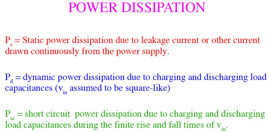
! Inverter Power. ! Dynamic Characteristics. " Delay ! P = I V. ! Tricky part: " Understanding I. " (pairing with correct V) ! Dynamic current flow:
 ! Dynamic current flow:") ESE 570: Digital Integrated ircuits and LSI Fundamentals Lecture Outline! Inverter Power! Dynamic haracteristics Lec 10: February 15, 2018 MOS Inverter: Dynamic haracteristics " Delay 3 Power Inverter
ESE 570: Digital Integrated ircuits and LSI Fundamentals Lecture Outline! Inverter Power! Dynamic haracteristics Lec 10: February 15, 2018 MOS Inverter: Dynamic haracteristics " Delay 3 Power Inverter
ESE 570: Digital Integrated Circuits and VLSI Fundamentals
 ESE 570: Digital Integrated Circuits and VLSI Fundamentals Lec 10: February 16, 2016 MOS Inverter: Dynamic Characteristics Lecture Outline! Review: Symmetric CMOS Inverter Design! Inverter Power! Dynamic
ECE 342 Solid State Devices & Circuits 4. CMOS
 ECE 34 Solid State Devices & Circuits 4. CMOS Jose E. Schutt-Aine Electrical & Computer Engineering University of Illinois jschutt@emlab.uiuc.edu ECE 34 Jose Schutt Aine 1 Digital Circuits V IH : Input
Digital Integrated Circuits 2nd Inverter
 Digital Integrated Circuits The Inverter The CMOS Inverter V DD Analysis Inverter complex gate Cost V in V out complexity & Area Integrity and robustness C L Static behavior Performance Dynamic response
EEC 116 Lecture #5: CMOS Logic. Rajeevan Amirtharajah Bevan Baas University of California, Davis Jeff Parkhurst Intel Corporation
 EEC 116 Lecture #5: CMOS Logic Rajeevan mirtharajah Bevan Baas University of California, Davis Jeff Parkhurst Intel Corporation nnouncements Quiz 1 today! Lab 2 reports due this week Lab 3 this week HW
2007 Fall: Electronic Circuits 2 CHAPTER 10. Deog-Kyoon Jeong School of Electrical Engineering
 007 Fall: Electronic Circuits CHAPTER 10 Digital CMOS Logic Circuits Deog-Kyoon Jeong dkjeong@snu.ac.kr k School of Electrical Engineering Seoul lnational luniversity it Introduction In this chapter, we
CARNEGIE MELLON UNIVERSITY DEPARTMENT OF ELECTRICAL AND COMPUTER ENGINEERING DIGITAL INTEGRATED CIRCUITS FALL 2002
 CARNEGIE MELLON UNIVERSITY DEPARTMENT OF ELECTRICAL AND COMPUTER ENGINEERING 18-322 DIGITAL INTEGRATED CIRCUITS FALL 2002 Final Examination, Monday Dec. 16, 2002 NAME: SECTION: Time: 180 minutes Closed
Midterm. ESE 570: Digital Integrated Circuits and VLSI Fundamentals. Lecture Outline. Pass Transistor Logic. Restore Output.
 ESE 570: Digital Integrated Circuits and VLSI Fundamentals Lec 16: March 21, 2017 Transmission Gates, Euler Paths, Energy Basics Review Midterm! Midterm " Mean: 79.5 " Standard Dev: 14.5 2 Lecture Outline!
ESE 570: Digital Integrated Circuits and VLSI Fundamentals
 ESE 570: Digital Integrated Circuits and VLSI Fundamentals Lec 15: March 15, 2018 Euler Paths, Energy Basics and Optimization Midterm! Midterm " Mean: 89.7 " Standard Dev: 8.12 2 Lecture Outline! Euler
The Physical Structure (NMOS)
") The Physical Structure (NMOS) Al SiO2 Field Oxide Gate oxide S n+ Polysilicon Gate Al SiO2 SiO2 D n+ L channel P Substrate Field Oxide contact Metal (S) n+ (G) L W n+ (D) Poly 1 Transistor Resistance Two
The Physical Structure (NMOS) Al SiO2 Field Oxide Gate oxide S n+ Polysilicon Gate Al SiO2 SiO2 D n+ L channel P Substrate Field Oxide contact Metal (S) n+ (G) L W n+ (D) Poly 1 Transistor Resistance Two
EEC 118 Lecture #6: CMOS Logic. Rajeevan Amirtharajah University of California, Davis Jeff Parkhurst Intel Corporation
 EEC 118 Lecture #6: CMOS Logic Rajeevan mirtharajah University of California, Davis Jeff Parkhurst Intel Corporation nnouncements Quiz 1 today! Lab 2 reports due this week Lab 3 this week HW 3 due this
The CMOS Inverter: A First Glance
 The CMOS Inverter: A First Glance V DD V in V out C L CMOS Properties Full rail-to-rail swing Symmetrical VTC Propagation delay function of load capacitance and resistance of transistors No static power
Very Large Scale Integration (VLSI)
") Very Large Scale Integration (VLSI) Lecture 4 Dr. Ahmed H. Madian Ah_madian@hotmail.com Dr. Ahmed H. Madian-VLSI Contents Delay estimation Simple RC model Penfield-Rubenstein Model Logical effort Delay
Very Large Scale Integration (VLSI) Lecture 4 Dr. Ahmed H. Madian Ah_madian@hotmail.com Dr. Ahmed H. Madian-VLSI Contents Delay estimation Simple RC model Penfield-Rubenstein Model Logical effort Delay
ESE 570 MOS INVERTERS STATIC (DC Steady State) CHARACTERISTICS. Kenneth R. Laker, University of Pennsylvania, updated 12Feb15
 CHARACTERISTICS. Kenneth R. Laker, University of Pennsylvania, updated 12Feb15") ESE 570 MOS INVERTERS STATIC (DC Steady State) CHARACTERISTICS 1 VDD Vout Vin Ideal VTC Logic 0 = 0 V Logic 1 = VDD 0 2 VOH VDD VOL 0 o.c. Cout For DC steady-state Cout is open circuit. VDD 0 VDD VOL VT0n
ESE 570 MOS INVERTERS STATIC (DC Steady State) CHARACTERISTICS 1 VDD Vout Vin Ideal VTC Logic 0 = 0 V Logic 1 = VDD 0 2 VOH VDD VOL 0 o.c. Cout For DC steady-state Cout is open circuit. VDD 0 VDD VOL VT0n
The CMOS Inverter: A First Glance
 The CMOS Inverter: A First Glance V DD S D V in V out C L D S CMOS Inverter N Well V DD V DD PMOS 2λ PMOS Contacts In Out In Out Metal 1 NMOS Polysilicon NMOS GND CMOS Inverter: Steady State Response V
ECE321 Electronics I
 ECE31 Electronics Lecture 1: CMOS nverter: Noise Margin & Delay Model Payman Zarkesh-Ha Office: ECE Bldg. 30B Office hours: Tuesday :00-3:00PM or by appointment E-mail: payman@ece.unm.edu Slide: 1 CMOS
University of Pennsylvania Department of Electrical Engineering. ESE 570 Midterm Exam March 14, 2013 FORMULAS AND DATA
 University of Pennsylvania Department of Electrical Engineering ESE 570 Midterm Exam March 4, 03 FORMULAS AND DATA. PHYSICAL CONSTANTS: n i = intrinsic concentration undoped) silicon =.45 x 0 0 cm -3 @
Chapter 5. The Inverter. V1. April 10, 03 V1.1 April 25, 03 V2.1 Nov Inverter
 Chapter 5 The Inverter V1. April 10, 03 V1.1 April 25, 03 V2.1 Nov.12 03 Objective of This Chapter Use Inverter to know basic CMOS Circuits Operations Watch for performance Index such as Speed (Delay calculation)
Lecture 5. MOS Inverter: Switching Characteristics and Interconnection Effects
 Lecture 5 MOS Inverter: Switching Characteristics and Interconnection Effects Introduction C load = (C gd,n + C gd,p + C db,n + C db,p ) + (C int + C g ) Lumped linear capacitance intrinsic cap. extrinsic
Practice 7: CMOS Capacitance
 Practice 7: CMOS Capacitance Digital Electronic Circuits Semester A 2012 MOSFET Capacitances MOSFET Capacitance Components 3 Gate to Channel Capacitance In general, the gate capacitance is similar to a
EEE 421 VLSI Circuits
 EEE 421 CMOS Properties Full rail-to-rail swing high noise margins» Logic levels not dependent upon the relative device sizes transistors can be minimum size ratioless Always a path to V dd or GND in steady
EE5311- Digital IC Design
 EE5311- Digital IC Design Module 3 - The Inverter Janakiraman V Assistant Professor Department of Electrical Engineering Indian Institute of Technology Madras Chennai September 3, 2018 Janakiraman, IITM
5.0 CMOS Inverter. W.Kucewicz VLSICirciuit Design 1
 5.0 CMOS Inverter W.Kucewicz VLSICirciuit Design 1 Properties Switching Threshold Dynamic Behaviour Capacitance Propagation Delay nmos/pmos Ratio Power Consumption Contents W.Kucewicz VLSICirciuit Design
Digital Microelectronic Circuits ( ) The CMOS Inverter. Lecture 4: Presented by: Adam Teman
 The CMOS Inverter. Lecture 4: Presented by: Adam Teman") Digital Microelectronic Circuits (361-1-301 ) Presented by: Adam Teman Lecture 4: The CMOS Inverter 1 Last Lectures Moore s Law Terminology» Static Properties» Dynamic Properties» Power The MOSFET Transistor»
Digital Microelectronic Circuits (361-1-301 ) Presented by: Adam Teman Lecture 4: The CMOS Inverter 1 Last Lectures Moore s Law Terminology» Static Properties» Dynamic Properties» Power The MOSFET Transistor»
ECE 342 Electronic Circuits. Lecture 35 CMOS Delay Model
 ECE 34 Electronic Circuits Lecture 35 CMOS Delay Model Jose E. Schutt-Aine Electrical & Computer Engineering University of Illinois jesa@illinois.edu ECE 34 Jose Schutt Aine 1 Digital Circuits V IH : Input
Digital Integrated Circuits
 Chapter 6 The CMOS Inverter 1 Contents Introduction (MOST models) 0, 1 st, 2 nd order The CMOS inverter : The static behavior: o DC transfer characteristics, o Short-circuit current The CMOS inverter :
Announcements. EE141- Spring 2003 Lecture 8. Power Inverter Chain
 - Spring 2003 Lecture 8 Power Inverter Chain Announcements Homework 3 due today. Homework 4 will be posted later today. Special office hours from :30-3pm at BWRC (in lieu of Tuesday) Today s lecture Power
ESE570 Spring University of Pennsylvania Department of Electrical and System Engineering Digital Integrated Cicruits AND VLSI Fundamentals
 University of Pennsylvania Department of Electrical and System Engineering Digital Integrated Cicruits AND VLSI Fundamentals ESE570, Spring 017 Final Wednesday, May 3 4 Problems with point weightings shown.
EE115C Digital Electronic Circuits Homework #6
 Problem 1 Sizing of adder blocks Electrical Engineering Department Spring 2010 EE115C Digital Electronic Circuits Homework #6 Solution Figure 1: Mirror adder. Study the mirror adder cell (textbook, pages
Fig. 1 CMOS Transistor Circuits (a) Inverter Out = NOT In, (b) NOR-gate C = NOT (A or B)
 Inverter Out = NOT In, (b) NOR-gate C = NOT (A or B)") 1 Introduction to Transistor-Level Logic Circuits 1 By Prawat Nagvajara At the transistor level of logic circuits, transistors operate as switches with the logic variables controlling the open or closed
1 Introduction to Transistor-Level Logic Circuits 1 By Prawat Nagvajara At the transistor level of logic circuits, transistors operate as switches with the logic variables controlling the open or closed
9/18/2008 GMU, ECE 680 Physical VLSI Design
 ECE680: Physical VLSI Design Chapter III CMOS Device, Inverter, Combinational circuit Logic and Layout Part 3 Combinational Logic Gates (textbook chapter 6) 9/18/2008 GMU, ECE 680 Physical VLSI Design
EE115C Digital Electronic Circuits Homework #4
 EE115 Digital Electronic ircuits Homework #4 Problem 1 Power Dissipation Solution Vdd =1.0V onsider the source follower circuit used to drive a load L =20fF shown above. M1 and M2 are both NMOS transistors
The Inverter. Digital Integrated Circuits A Design Perspective. Jan M. Rabaey Anantha Chandrakasan Borivoje Nikolic
 Digital Integrated Circuits A Design Perspective Jan M. Rabaey Anantha Chandrakasan Borivoje Nikolic The Inverter Revised from Digital Integrated Circuits, Jan M. Rabaey el, 2003 Propagation Delay CMOS
ENEE 359a Digital VLSI Design
 SLIDE 1 ENEE 359a Digital VLSI Design & Logical Effort Prof. blj@ece.umd.edu Credit where credit is due: Slides contain original artwork ( Jacob 2004) as well as material taken liberally from Irwin & Vijay
Lecture 4: CMOS review & Dynamic Logic
 Lecture 4: CMOS review & Dynamic Logic Reading: ch5, ch6 Overview CMOS basics Power and energy in CMOS Dynamic logic 1 CMOS Properties Full rail-to-rail swing high noise margins Logic levels not dependent
Integrated Circuits & Systems
 Federal University of Santa Catarina Center for Technology Computer Science & Electronics Engineering Integrated Circuits & Systems INE 5442 Lecture 14 The CMOS Inverter: dynamic behavior (sizing, inverter
Integrated Circuits & Systems
 Federal University of Santa Catarina Center for Technology Computer Science & Electronics Engineering Integrated Circuits & Systems INE 5442 Lecture 13 The CMOS Inverter: dynamic behavior (delay) guntzel@inf.ufsc.br
EE5780 Advanced VLSI CAD
 EE5780 Advanced VLSI CAD Lecture 4 DC and Transient Responses, Circuit Delays Zhuo Feng 4.1 Outline Pass Transistors DC Response Logic Levels and Noise Margins Transient Response RC Delay Models Delay
Spiral 2 7. Capacitance, Delay and Sizing. Mark Redekopp
 2-7.1 Spiral 2 7 Capacitance, Delay and Sizing Mark Redekopp 2-7.2 Learning Outcomes I understand the sources of capacitance in CMOS circuits I understand how delay scales with resistance, capacitance
Lecture Outline. ESE 570: Digital Integrated Circuits and VLSI Fundamentals. Review: 1st Order RC Delay Models. Review: Two-Input NOR Gate (NOR2)
") ESE 570: Digital Integrated Circuits and VLSI Fundamentals Lec 14: March 1, 2016 Combination Logic: Ratioed and Pass Logic Lecture Outline! CMOS Gates Review " CMOS Worst Case Analysis! Ratioed Logic Gates!
ESE 570: Digital Integrated Circuits and VLSI Fundamentals Lec 14: March 1, 2016 Combination Logic: Ratioed and Pass Logic Lecture Outline! CMOS Gates Review " CMOS Worst Case Analysis! Ratioed Logic Gates!
EE5311- Digital IC Design
 EE5311- Digital IC Design Module 3 - The Inverter Janakiraman V Assistant Professor Department of Electrical Engineering Indian Institute of Technology Madras Chennai September 6, 2017 Janakiraman, IITM
Lecture 5: DC & Transient Response
 Lecture 5: DC & Transient Response Outline q Pass Transistors q DC Response q Logic Levels and Noise Margins q Transient Response q RC Delay Models q Delay Estimation 2 Activity 1) If the width of a transistor
Properties of CMOS Gates Snapshot
 MOS logic 1 Properties of MOS Gates Snapshot High noise margins: V OH and V OL are at V DD and GND, respectively. No static power consumption: There never exists a direct path between V DD and V SS (GND)
CMPEN 411 VLSI Digital Circuits Spring 2012
 CMPEN 411 VLSI Digital Circuits Spring 2012 Lecture 09: Resistance & Inverter Dynamic View [Adapted from Rabaey s Digital Integrated Circuits, Second Edition, 2003 J. Rabaey, A. Chandrakasan, B. Nikolic]
Interconnect (2) Buffering Techniques. Logical Effort
 Buffering Techniques. Logical Effort") Interconnect (2) Buffering Techniques. Logical Effort Lecture 14 18-322 Fall 2002 Textbook: [Sections 4.2.1, 8.2.3] A few announcements! M1 is almost over: The check-off is due today (by 9:30PM) Students
Interconnect (2) Buffering Techniques. Logical Effort Lecture 14 18-322 Fall 2002 Textbook: [Sections 4.2.1, 8.2.3] A few announcements! M1 is almost over: The check-off is due today (by 9:30PM) Students
Lecture 4: DC & Transient Response
 Introduction to CMOS VLSI Design Lecture 4: DC & Transient Response David Harris Harvey Mudd College Spring 004 Outline DC Response Logic Levels and Noise Margins Transient Response Delay Estimation Slide
DC and Transient. Courtesy of Dr. Daehyun Dr. Dr. Shmuel and Dr.
 DC and Transient Courtesy of Dr. Daehyun Lim@WSU, Dr. Harris@HMC, Dr. Shmuel Wimer@BIU and Dr. Choi@PSU http://csce.uark.edu +1 (479) 575-604 yrpeng@uark.edu Pass Transistors We have assumed source is
EECS 141: FALL 05 MIDTERM 1
 University of California College of Engineering Department of Electrical Engineering and Computer Sciences D. Markovic TuTh 11-1:3 Thursday, October 6, 6:3-8:pm EECS 141: FALL 5 MIDTERM 1 NAME Last SOLUTION
CMPEN 411 VLSI Digital Circuits. Lecture 04: CMOS Inverter (static view)
") CMPEN 411 VLSI Digital Circuits Lecture 04: CMOS Inverter (static view) Kyusun Choi [Adapted from Rabaey s Digital Integrated Circuits, Second Edition, 2003 J. Rabaey, A. Chandrakasan, B. Nikolic] CMPEN
CMPEN 411 VLSI Digital Circuits Lecture 04: CMOS Inverter (static view) Kyusun Choi [Adapted from Rabaey s Digital Integrated Circuits, Second Edition, 2003 J. Rabaey, A. Chandrakasan, B. Nikolic] CMPEN
EE115C Digital Electronic Circuits Homework #5
 EE115C Digital Electronic Circuits Homework #5 Due Thursday, May 13, 6pm @ 56-147E EIV Problem 1 Elmore Delay Analysis Calculate the Elmore delay from node A to node B using the values for the resistors
EE 560 MOS INVERTERS: DYNAMIC CHARACTERISTICS. Kenneth R. Laker, University of Pennsylvania
 1 EE 560 MOS INVERTERS: DYNAMIC CHARACTERISTICS C gsp V DD C sbp C gd, C gs, C gb -> Oxide Caps C db, C sb -> Juncion Caps 2 S C in -> Ineconnec Cap G B D C dbp V in C gdp V ou C gdn D C dbn G B S C in
4.10 The CMOS Digital Logic Inverter
 11/11/2004 section 4_10 The CMOS Digital Inverter blank.doc 1/1 4.10 The CMOS Digital Logic Inverter Reading Assignment: pp. 336346 Complementary MOSFET (CMOS) is the predominant technology for constructing
ESE570 Spring University of Pennsylvania Department of Electrical and System Engineering Digital Integrated Cicruits AND VLSI Fundamentals
 University of Pennsylvania Department of Electrical and System Engineering Digital Integrated Cicruits AND VLSI Fundamentals ESE570, Spring 2018 Final Monday, Apr 0 5 Problems with point weightings shown.
MOSFET and CMOS Gate. Copy Right by Wentai Liu
 MOSFET and CMOS Gate CMOS Inverter DC Analysis - Voltage Transfer Curve (VTC) Find (1) (2) (3) (4) (5) (6) V OH min, V V OL min, V V IH min, V V IL min, V OHmax OLmax IHmax ILmax NM L = V ILmax V OL max
EE 330 Lecture 39. Digital Circuits. Propagation Delay basic characterization Device Sizing (Inverter and multiple-input gates)
") EE 330 Lecture 39 Digital ircuits Propagation Delay basic characterization Device Sizing (Inverter and multiple-input gates) Review from last lecture Other MOS Logic Families Enhancement Load NMOS Enhancement
EE 330 Lecture 39 Digital ircuits Propagation Delay basic characterization Device Sizing (Inverter and multiple-input gates) Review from last lecture Other MOS Logic Families Enhancement Load NMOS Enhancement
Lecture 14 - Digital Circuits (III) CMOS. April 1, 2003
 CMOS. April 1, 2003") 6.12 - Microelectronic Devices and Circuits - Spring 23 Lecture 14-1 Lecture 14 - Digital Circuits (III) CMOS April 1, 23 Contents: 1. Complementary MOS (CMOS) inverter: introduction 2. CMOS inverter:
6.12 - Microelectronic Devices and Circuits - Spring 23 Lecture 14-1 Lecture 14 - Digital Circuits (III) CMOS April 1, 23 Contents: 1. Complementary MOS (CMOS) inverter: introduction 2. CMOS inverter:
High-to-Low Propagation Delay t PHL
 High-to-Low Propagation Delay t PHL V IN switches instantly from low to high. Driver transistor (n-channel) immediately switches from cutoff to saturation; the p-channel pull-up switches from triode to
Integrated Circuits & Systems
 Federal University of Santa Catarina Center for Technology Computer Science & Electronics Engineering Integrated Circuits & Systems INE 5442 Lecture 16 CMOS Combinational Circuits - 2 guntzel@inf.ufsc.br
Lecture 12 CMOS Delay & Transient Response
 EE 471: Transport Phenomena in Solid State Devices Spring 2018 Lecture 12 CMOS Delay & Transient Response Bryan Ackland Department of Electrical and Computer Engineering Stevens Institute of Technology
Homework Assignment #5 EE 477 Spring 2017 Professor Parker
 Homework Assignment #5 EE 477 Spring 2017 Professor Parker Question 1: (15%) Compute the worst-case rising and falling RC time constants at point B of the circuit below using the Elmore delay method. Assume
ECE 438: Digital Integrated Circuits Assignment #4 Solution The Inverter
 ECE 438: Digital Integrated Circuits Assignment #4 The Inverter Text: Chapter 5, Digital Integrated Circuits 2 nd Ed, Rabaey 1) Consider the CMOS inverter circuit in Figure P1 with the following parameters.
VLSI GATE LEVEL DESIGN UNIT - III P.VIDYA SAGAR ( ASSOCIATE PROFESSOR) Department of Electronics and Communication Engineering, VBIT
 Department of Electronics and Communication Engineering, VBIT") VLSI UNIT - III GATE LEVEL DESIGN P.VIDYA SAGAR ( ASSOCIATE PROFESSOR) contents GATE LEVEL DESIGN : Logic Gates and Other complex gates, Switch logic, Alternate gate circuits, Time Delays, Driving large
VLSI UNIT - III GATE LEVEL DESIGN P.VIDYA SAGAR ( ASSOCIATE PROFESSOR) contents GATE LEVEL DESIGN : Logic Gates and Other complex gates, Switch logic, Alternate gate circuits, Time Delays, Driving large
Interconnect (2) Buffering Techniques.Transmission Lines. Lecture Fall 2003
 Buffering Techniques.Transmission Lines. Lecture Fall 2003") Interconnect (2) Buffering Techniques.Transmission Lines Lecture 12 18-322 Fall 2003 A few announcements Partners Lab Due Times Midterm 1 is nearly here Date: 10/14/02, time: 3:00-4:20PM, place: in class
Interconnect (2) Buffering Techniques.Transmission Lines Lecture 12 18-322 Fall 2003 A few announcements Partners Lab Due Times Midterm 1 is nearly here Date: 10/14/02, time: 3:00-4:20PM, place: in class
PASS-TRANSISTOR LOGIC. INEL Fall 2014
 PASS-TRANSISTOR LOGIC INEL 4207 - Fall 2014 Figure 15.5 Conceptual pass-transistor logic gates. (a) Two switches, controlled by the input variables B and C, when connected in series in the path between
Topics to be Covered. capacitance inductance transmission lines
 Topics to be Covered Circuit Elements Switching Characteristics Power Dissipation Conductor Sizes Charge Sharing Design Margins Yield resistance capacitance inductance transmission lines Resistance of
EE 330 Lecture 37. Digital Circuits. Other Logic Families. Propagation Delay basic characterization Device Sizing (Inverter and multiple-input gates)
") EE 330 Lecture 37 Digital Circuits Other Logic Families Static Power Dissipation Propagation Delay basic characterization Device Sizing (Inverter and multiple-input gates) Review from Last Time Inverter
EE 330 Lecture 37 Digital Circuits Other Logic Families Static Power Dissipation Propagation Delay basic characterization Device Sizing (Inverter and multiple-input gates) Review from Last Time Inverter
Lecture 6: DC & Transient Response
 Lecture 6: DC & Transient Response Slides courtesy of Deming Chen Slides based on the initial set from David Harris CMOS VLSI Design Outline Pass Transistors DC Response Logic Levels and Noise Margins
Homework #2 10/6/2016. C int = C g, where 1 t p = t p0 (1 + C ext / C g ) = t p0 (1 + f/ ) f = C ext /C g is the effective fanout
 = t p0 (1 + f/ ) f = C ext /C g is the effective fanout") 0/6/06 Homework # Lecture 8, 9: Sizing and Layout of omplex MOS Gates Reading: hapter 4, sections 4.3-4.5 October 3 & 5, 06 hapter, section.5.5 Prof. R. Iris ahar Weste & Harris vailable on course webpage
0/6/06 Homework # Lecture 8, 9: Sizing and Layout of omplex MOS Gates Reading: hapter 4, sections 4.3-4.5 October 3 & 5, 06 hapter, section.5.5 Prof. R. Iris ahar Weste & Harris vailable on course webpage
EE213, Spr 2017 HW#3 Due: May 17 th, in class. Figure 1
 RULES: Please try to work on your own. Discussion is permissible, but identical submissions are unacceptable! Please show all intermediate steps: a correct solution without an explanation will get zero
Lecture 5: DC & Transient Response
 Lecture 5: DC & Transient Response Outline Pass Transistors DC Response Logic Levels and Noise Margins Transient Response RC Delay Models Delay Estimation 2 Pass Transistors We have assumed source is grounded
Power Consumption in CMOS CONCORDIA VLSI DESIGN LAB
 Power Consumption in CMOS 1 Power Dissipation in CMOS Two Components contribute to the power dissipation:» Static Power Dissipation Leakage current Sub-threshold current» Dynamic Power Dissipation Short
Digital Integrated Circuits A Design Perspective
 igital Integrated Circuits esign Perspective esigning Combinational Logic Circuits 1 Combinational vs. Sequential Logic In Combinational Logic Circuit Out In Combinational Logic Circuit Out State Combinational
CS/EE N-type Transistor
 CS/EE 6710 MOS Transistor Models Electrical Effects Propagation Delay N-type Transistor D + G Vds i electrons +Vgs S - 1 Another Cutaway View Thanks to National Central University for Some images Vgs Forms
Digital Integrated Circuits A Design Perspective
 Digital Integrated Circuits Design Perspective Jan M. Rabaey nantha Chandrakasan orivoje Nikolić Designing Combinational Logic Circuits November 2002. 1 Combinational vs. Sequential Logic In Combinational
Review of Band Energy Diagrams MIS & MOS Capacitor MOS TRANSISTORS MOSFET Capacitances MOSFET Static Model
 Content- MOS Devices and Switching Circuits Review of Band Energy Diagrams MIS & MOS Capacitor MOS TRANSISTORS MOSFET Capacitances MOSFET Static Model A Cantoni 2009-2013 Digital Switching 1 Content- MOS
Digital Integrated Circuits. The Wire * Fuyuzhuo. *Thanks for Dr.Guoyong.SHI for his slides contributed for the talk. Digital IC.
 Digital Integrated Circuits The Wire * Fuyuzhuo *Thanks for Dr.Guoyong.SHI for his slides contributed for the talk Introduction The Wire transmitters receivers schematics physical 2 Interconnect Impact
Announcements. EE141- Fall 2002 Lecture 7. MOS Capacitances Inverter Delay Power
 - Fall 2002 Lecture 7 MOS Capacitances Inverter Delay Power Announcements Wednesday 12-3pm lab cancelled Lab 4 this week Homework 2 due today at 5pm Homework 3 posted tonight Today s lecture MOS capacitances
Chapter 11. Inverter. DC AC, Switching. Layout. Sizing PASS GATES (CHPT 10) Other Inverters. Baker Ch. 11 The Inverter. Introduction to VLSI
 Other Inverters. Baker Ch. 11 The Inverter. Introduction to VLSI") Chapter 11 Inverter DC AC, Switching Ring Oscillator Dynamic Power Dissipation Layout LATCHUP Sizing PASS GATES (CHPT 10) Other Inverters Joseph A. Elias, Ph.D. Adjunct Professor, University of Kentucky;
Chapter 11 Inverter DC AC, Switching Ring Oscillator Dynamic Power Dissipation Layout LATCHUP Sizing PASS GATES (CHPT 10) Other Inverters Joseph A. Elias, Ph.D. Adjunct Professor, University of Kentucky;
ESE 570: Digital Integrated Circuits and VLSI Fundamentals
 ESE 570: Digital Integrated Circuits and VLSI Fundamentals Lec 18: March 27, 2018 Dynamic Logic, Charge Injection Lecture Outline! Sequential MOS Logic " D-Latch " Timing Constraints! Dynamic Logic " Domino
Lecture 7 Circuit Delay, Area and Power
 Lecture 7 Circuit Delay, Area and Power lecture notes from S. Mitra Intro VLSI System course (EE271) Introduction to VLSI Systems 1 Circuits and Delay Introduction to VLSI Systems 2 Power, Delay and Area:
CMOS Inverter (static view)
") Review: Design Abstraction Levels SYSTEM CMOS Inverter (static view) + MODULE GATE [Adapted from Chapter 5. 5.3 CIRCUIT of G DEVICE Rabaey s Digital Integrated Circuits,, J. Rabaey et al.] S D Review:
Review: Design Abstraction Levels SYSTEM CMOS Inverter (static view) + MODULE GATE [Adapted from Chapter 5. 5.3 CIRCUIT of G DEVICE Rabaey s Digital Integrated Circuits,, J. Rabaey et al.] S D Review:
Chapter 5 CMOS Logic Gate Design
 Chapter 5 CMOS Logic Gate Design Section 5. -To achieve correct operation of integrated logic gates, we need to satisfy 1. Functional specification. Temporal (timing) constraint. (1) In CMOS, incorrect
ENGR890 Digital VLSI Design Fall Lecture 4: CMOS Inverter (static view)
") ENGR89 Digital VLSI Design Fall 5 Lecture 4: CMOS Inverter (static view) [Adapted from Chapter 5 of Digital Integrated Circuits, 3, J. Rabaey et al.] [Also borrowed from Vijay Narayanan and Mary Jane Irwin]
ENGR89 Digital VLSI Design Fall 5 Lecture 4: CMOS Inverter (static view) [Adapted from Chapter 5 of Digital Integrated Circuits, 3, J. Rabaey et al.] [Also borrowed from Vijay Narayanan and Mary Jane Irwin]
EE241 - Spring 2000 Advanced Digital Integrated Circuits. Announcements
 EE241 - Spring 2000 Advanced Digital Integrated Circuits Lecture 3 Circuit Optimization for Speed Announcements Tu 2/8/00 class will be pre-taped on Friday, 2/4, 4-5:30 203 McLaughlin Class notes are available
EE141Microelettronica. CMOS Logic
 Microelettronica CMOS Logic CMOS logic Power consumption in CMOS logic gates Where Does Power Go in CMOS? Dynamic Power Consumption Charging and Discharging Capacitors Short Circuit Currents Short Circuit
5. CMOS Gate Characteristics CS755
 5. CMOS Gate Characteristics Last module: CMOS Transistor theory This module: DC Response Logic Levels and Noise Margins Transient Response Delay Estimation Transistor ehavior 1) If the width of a transistor
Name: Grade: Q1 Q2 Q3 Q4 Q5 Total. ESE370 Fall 2015
 University of Pennsylvania Department of Electrical and System Engineering Circuit-Level Modeling, Design, and Optimization for Digital Systems ESE370, Fall 205 Midterm Wednesday, November 4 Point values
Lecture 9: Interconnect
 Digital Integrated Circuits (83-313) Lecture 9: Interconnect Semester B, 2016-17 Lecturer: Dr. Adam Teman TAs: Itamar Levi, Robert Giterman 23 May 2017 Disclaimer: This course was prepared, in its entirety,
EE 434 Lecture 33. Logic Design
 EE 434 Lecture 33 Logic Design Review from last time: Ask the inverter how it will interpret logic levels V IN V OUT V H =? V L =? V LARGE V H V L V H Review from last time: The two-inverter loop X Y X
Using MOS Models. C.K. Ken Yang UCLA Courtesy of MAH EE 215B
 Using MOS Models C.K. Ken Yang UCLA yangck@ucla.edu Courtesy of MAH 1 Overview Reading Rabaey 5.4 W&H 4.2 Background In the past two lectures we have reviewed the iv and CV curves for MOS devices, both
EE141. Administrative Stuff
 -Spring 2004 Digital Integrated ircuits Lecture 15 Logical Effort Pass Transistor Logic 1 dministrative Stuff First (short) project to be launched next Th. Overall span: 1 week Hardware lab this week Hw
EE 560 CHIP INPUT AND OUTPUT (I/0) CIRCUITS. Kenneth R. Laker, University of Pennsylvania
 CIRCUITS. Kenneth R. Laker, University of Pennsylvania") 1 EE 560 CHIP INPUT AND OUTPUT (I/0) CIRCUITS 2 -> ESD PROTECTION CIRCUITS (INPUT PADS) -> ON-CHIP CLOCK GENERATION & DISTRIBUTION -> OUTPUT PADS -> ON-CHIP NOISE DUE TO PARASITIC INDUCTANCE -> SUPER BUFFER
1 EE 560 CHIP INPUT AND OUTPUT (I/0) CIRCUITS 2 -> ESD PROTECTION CIRCUITS (INPUT PADS) -> ON-CHIP CLOCK GENERATION & DISTRIBUTION -> OUTPUT PADS -> ON-CHIP NOISE DUE TO PARASITIC INDUCTANCE -> SUPER BUFFER
ESE 570: Digital Integrated Circuits and VLSI Fundamentals
 ESE 570: Digital Integrated Circuits and VLSI Fundamentals Lec 15: March 3, 2016 Combination Logic: Ratioed & Pass Logic, and Performance Lecture Outline! CMOS NOR2 Worst Case Analysis! Pass Transistor