een an axiom of mine tle things are infinitely the most impo Conan Doyle Danny Porath 2003
|
|
|
- Bennett Ramsey
- 6 years ago
- Views:
Transcription

1 gle Electron Tunneling Artificial Atoms een an axiom of mine tle things are infinitely the most impo Conan Doyle Danny Porath 003 (K
2 ased on works by. ian Shönenberger - present oph Wasshuber Ph.D. Th ntin Likharev IEEE 87, 60 Meirave and E.B. Fo ductor Science and Technology, ouwenhoven Reviews (see si Millo - presentation
3 ooks and Internet Sites ransport in Mesoscopic Systems ge Tunneling, H. Grabert & M ction to Mesoscopic Physics, Y.iue.tuwien.ac.at/publications/PhD%0Theses/w p://vortex.tn.tudelft.nl/grkouwen/reviewpub.htm ww.aip.org/web/aiphome/pt/vol-54/iss-5/archiv ton.edu/~chouweb/newproject/research/qdt/si
4 r: Homework 7 ms, Mark Kastner, Physics Today, Janu r: ts, L. Kouwenhoven and C. Marcus, Ph 35. r: he Coulomb staircase in a two-junction tron charge, a and M. Tinkham, Physical Review B,
5 Outline SET: sic concept thodox theory eneral treatment uble barrier tunnel junction ulomb staircase gle electron transistor ability diagram
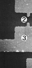
6
7 ices (SET Devices), based on the single electrons between smal ve already enabled several importa. Several other applications of an vices in unique scientific instrume eem quite feasible. On the othe silicon transistors being replaced ices in integrated digital circuits nd remains uncertain. Neverthele ment does not happen, single-ele play an important role by shedding size limitations of new electro recent research in this field ha ng by-product ideas which may ss-memory and digital-d
8 Law For many Elec V=IR I V
9 ic Concept of Single Ele e After of a single uncompensated electron c field E which may prevent the add
10 The Charging Energy g energy: E C = e C rticle or the quantum dot (QD) size i ron De-Broglie wavelength, energy tantial on addition energy: a = E + k E C E k - e Kinetic E k = g(ef )V V- Volume g(e F )
11 ulomb Blockade and Sta nnel TJ or tion Capacitor CS QD V thresh CB blockade b staircase ts can be observed if: e h K T > B RT
12 e Motion and Quantiza
13 Various Capacitors
14 The Charging Energy round 3D ball with a free, degenera n=0 cm -3, electron effective mass m matrix (dielectric constant ε=4), with 0
15 The Charging Energy => Molecules SET effects at RT QD size -0 nm (=> E a ~ ev - 50 mev hermally induced tunneling E a s ~0-00 K B T quires: E a ~ ev => ~ nm e range there is a strong depe ape.
16 ergy Change Upon e Ad h 3 ( 3π n) n- carrier con
17 rgy Change Upon e Add Si and Al
18 Realizations of Quantu tor DEG:
19
20 dox Theory Major Ass Spectrum - the electr n inside the conductors is ignor ergy spectrum is treated as eaking this assumption is va but it frequently gives an of observations as soon as E k << us tunneling - the time τ t hrough the barrier is assum mall in comparison with other he interval between neighbori is assumption is valid for tun gle-electron devices of practic
21 dox Theory Major Ass quantum processes consisting s tunneling events ("co-tunn is assumption is valid if the r tunnel barriers of the syste the quantum unit of resistance R T >>R Q, R Q =h/4e 6.5 k and shape are ignored 0D Q us charge redistribution after ctra at the leads are continues limitations, the orthodox theo D s and most of the data for SC
22 The Orthodox Theory ng of a single electron through rier is always a random eve e Γ (i.e. probability per unit lely on the reduction W tic) energy of the system as ng event. = e I W e o W k T B W) e "seed dc I-V curve of the tunnel ingle-electron charging effects.
23 The Orthodox Theory following general expressions are rath Or: W = W = e(v e(v e i + i V ) voltage drops across the barrier be event. iprocal capacitance matrix of the sys f V ) [ t e(c ) kl (C ) kk + (C t
24 eling Rate vs. The Ener only tunneling events decreasing the dissipating the difference) are possib
25 Diagram of a Tunnel Ju explains why Γ W at W>>k B T proportional to the number of occ e electron source, which contribute
26
27 neral Treatment of The C N q = ϕ (i =,,..., N i C ij j= j c = N i= qϕ = i i N N i= j= (C - ) ij q i er of islands capacitances, C ij the inter-islands c iprocal capacitance matrix of the syst ions contact potentials bers of the islands separated by the
28 etailed Treatment - Tran robability amplitudes of the electron sion probability can be derived from EΨ. robability: 3 B B T = k k k k 8 k k k k + CO robability for a rectangular barrier: m * E m * (E k h = B
29 ransmission Probabilitie m *E 0 α-decay Atom ionization
30 The Tunnel Rate e from initial state i to a final state f f π h ( F) = T δ( E E k,k e difference in initial and final free e el rate: i f e E E k T B F T k,k i f(e ) rmi-dirac distribution f i i f ( -f(e )) δ( -f(e) = i f f E f(-e)
31 ct of the Fermi Function ape at the Relevant Tem
32 The Tunnel Barrier rs we can approximate T kikf ~ T : T i f f(e ) i ( -f(e )) δ( f E E c.i de i E c,f de D (E )D (E f i i f )f(e )( -f(e ) initial and final states of the conduc The DOS on the initial and final side tant D s and δ function reduction: π = h ) T DD def(e) ( -f(e- i f E c f i f
33 he Tunneling Resistance of charging we get a straight line (O ntroduce the tunneling resistance R T istance incorporates the transmission istance: get: - F e F k T B R T h = πe T T=0 DD At T=0: f Γ( F) = i
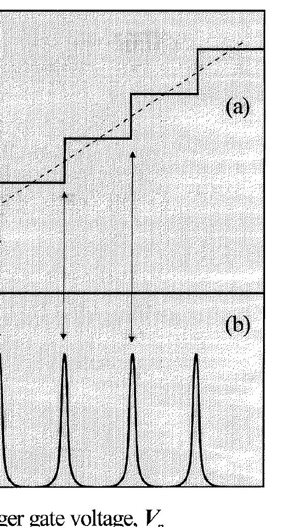
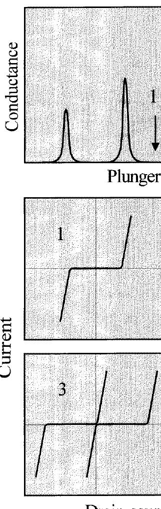
34 m Tunnel Resistance fo Electron Charging anically the electrons are not localiz er than N electrons on the island. -<N> uncertainty principle: E t > h R T C E = R T > h e = R Q 6kΩ
35
36 ouble Barrier Tunnel Ju, q =C V, q=(q -q +q 0 )=ne q 0 =(C Φ -C Φ )/e charge, induced by stray capacitances
37 ouble Barrier Tunnel Ju drop: b + ne q0 CV b V = CΣ Σ = C + C b = V V + V energy: q C + q C = C C V b + (ne C Σ q charge, induced by stray capacitances
38 Change in The Free Ene ne by the voltage source in tun nevb C C ergy of the complete circuit is: n W = Σ C Σ ( C C V + (ne q ) ) b W = nevb C C 0 Σ + ev in the free energy upon tunnelin e e ±,n ) F(n,n ) = ± ( Vb C C Σ n,n e e ± ) F(n,n ) = ± ( Vb C C + +
39 Change in The Free Ene erm in the above equations causes voltage V b exceeds a threshold voltag capacitance min(c,c ) V > b e C Σ This is the Coulomb blockade q 0 =0
40
41 The Coulomb Staircase ectron tunnels in/out of the island t s, it is favorable for another elect ther junction. number of electrons on the island a given voltage drop.
42 c Junctions - The Coulom <R T =R T Staircase appear: The coulomb staircase
43
44 ngle Electron Transistor ctrode the background charge q can b ing a third gate electrode we g single electron transistor trode controls the source-drain curre
45 ation of the Previous Eq C = C + C + C is: so: drop: = V q = ne + q0 + Cg (Vg V ( C + C ) = q g C V b V + b C g C C C Σ V g g Σ ( V ) 0 q0 + Cg g V V g + ne ne + q 0 q 0
46 ification of the Free En in the free energy upon tunnelin (( ) + ± = b g Σ V C C e C e ) F(n,n ) ( + ± = ± g b Σ C V V C e C e ) F(n,n )
47 Example
48
49 The Stability Diagram onditions enable to draw a stabi oscillations:
50 Summary effects are dominant nic behavior of small objec portant effects: CB & CS thodox theory uble barrier tunnel junction electron transistors y diagrams describe the pe of these small systems
Single Electron Tunneling Examples
 Single Electron Tunneling Examples Danny Porath 2002 (Schönenberger et. al.) It has long been an axiom of mine that the little things are infinitely the most important Sir Arthur Conan Doyle Books and
Building blocks for nanodevices
 Building blocks for nanodevices Two-dimensional electron gas (2DEG) Quantum wires and quantum point contacts Electron phase coherence Single-Electron tunneling devices - Coulomb blockage Quantum dots (introduction)
Chapter 8: Coulomb blockade and Kondo physics
 Chater 8: Coulomb blockade and Kondo hysics 1) Chater 15 of Cuevas& Scheer. REFERENCES 2) Charge transort and single-electron effects in nanoscale systems, J.M. Thijssen and H.S.J. Van der Zant, Phys.
Single Electron Transistor (SET)
") Single Electron Transistor (SET) e - e - dot C g V g A single electron transistor is similar to a normal transistor (below), except 1) the channel is replaced by a small dot. 2) the dot is separated from
Single Electron Transistor (SET) e - e - dot C g V g A single electron transistor is similar to a normal transistor (below), except 1) the channel is replaced by a small dot. 2) the dot is separated from
Single Electron Transistor (SET)
") Single Electron Transistor (SET) SET: e - e - dot A single electron transistor is similar to a normal transistor (below), except 1) the channel is replaced by a small dot. C g 2) the dot is separated from
Single Electron Transistor (SET) SET: e - e - dot A single electron transistor is similar to a normal transistor (below), except 1) the channel is replaced by a small dot. C g 2) the dot is separated from
single-electron electron tunneling (SET)
") single-electron electron tunneling (SET) classical dots (SET islands): level spacing is NOT important; only the charging energy (=classical effect, many electrons on the island) quantum dots: : level spacing
single-electron electron tunneling (SET) classical dots (SET islands): level spacing is NOT important; only the charging energy (=classical effect, many electrons on the island) quantum dots: : level spacing
Coulomb Blockade and Kondo Effect in Nanostructures
 Coulomb Blockade and Kondo Effect in Nanostructures Marcin M. Wysokioski 1,2 1 Institute of Physics Albert-Ludwigs-Universität Freiburg 2 Institute of Physics Jagiellonian University, Cracow, Poland 2.VI.2010
Charge spectrometry with a strongly coupled superconducting single-electron transistor
 PHYSICAL REVIEW B, VOLUME 64, 245116 Charge spectrometry with a strongly coupled superconducting single-electron transistor C. P. Heij, P. Hadley, and J. E. Mooij Applied Physics and Delft Institute of
Nanoelectronics. Topics
 Nanoelectronics Topics Moore s Law Inorganic nanoelectronic devices Resonant tunneling Quantum dots Single electron transistors Motivation for molecular electronics The review article Overview of Nanoelectronic
Semiconductor Physics fall 2012 problems
 Semiconductor Physics fall 2012 problems 1. An n-type sample of silicon has a uniform density N D = 10 16 atoms cm -3 of arsenic, and a p-type silicon sample has N A = 10 15 atoms cm -3 of boron. For each
Emerging Research Devices: A Study of CNTFET and SET as a replacement for SiMOSFET
 1 Emerging Research Devices: A Study of CNTFET and SET as a replacement for SiMOSFET Mahmoud Lababidi, Krishna Natarajan, Guangyu Sun Abstract Since the development of the Silicon MOSFET, it has been the
Study On the Capacitance Between Orbitals and Atoms Modeling
 Study On the Capacitance Between Orbitals and Atoms Modeling Ali A. Elabd *, El-Sayed M. El-Rabaie, Abdel-Aziz T. Shalaby Faculty of Electronic Engineering, 32952 Menouf, Minoufiya University, Egypt. In
New Model for Drain and Gate Current of Single-Electron Transistor at High Temperature
 World Journal of Nano Science and Engineering, 2012, 2, 171-175 http://dx.doi.org/10.4236/wjnse.2012.24022 Published Online ecember 2012 (http://www.scirp.org/journal/wjnse) New Model for rain and ate
Solid State Device Fundamentals
 Solid State Device Fundamentals ENS 345 Lecture Course by Alexander M. Zaitsev alexander.zaitsev@csi.cuny.edu Tel: 718 982 2812 Office 4N101b 1 Outline - Goals of the course. What is electronic device?
SPIN-POLARIZED CURRENT IN A MAGNETIC TUNNEL JUNCTION: MESOSCOPIC DIODE BASED ON A QUANTUM DOT
 66 Rev.Adv.Mater.Sci. 14(2007) 66-70 W. Rudziński SPIN-POLARIZED CURRENT IN A MAGNETIC TUNNEL JUNCTION: MESOSCOPIC DIODE BASED ON A QUANTUM DOT W. Rudziński Department of Physics, Adam Mickiewicz University,
Tunneling transport. Courtesy Prof. S. Sawyer, RPI Also Davies Ch. 5
 unneling transport Courtesy Prof. S. Sawyer, RPI Also Davies Ch. 5 Electron transport properties l e : electronic mean free path l φ : phase coherence length λ F : Fermi wavelength ecture Outline Important
Appendix 1: List of symbols
 Appendix 1: List of symbols Symbol Description MKS Units a Acceleration m/s 2 a 0 Bohr radius m A Area m 2 A* Richardson constant m/s A C Collector area m 2 A E Emitter area m 2 b Bimolecular recombination
Electronic transport in low dimensional systems
 Electronic transport in low dimensional systems For example: 2D system l
Mesoscopic Nano-Electro-Mechanics of Shuttle Systems
 * Mesoscopic Nano-Electro-Mechanics of Shuttle Systems Robert Shekhter University of Gothenburg, Sweden Lecture1: Mechanically assisted single-electronics Lecture2: Quantum coherent nano-electro-mechanics
How a single defect can affect silicon nano-devices. Ted Thorbeck
 How a single defect can affect silicon nano-devices Ted Thorbeck tedt@nist.gov The Big Idea As MOS-FETs continue to shrink, single atomic scale defects are beginning to affect device performance Gate Source
Chapter 3 Properties of Nanostructures
 Chapter 3 Properties of Nanostructures In Chapter 2, the reduction of the extent of a solid in one or more dimensions was shown to lead to a dramatic alteration of the overall behavior of the solids. Generally,
Analysis of flip flop design using nanoelectronic single electron transistor
 Int. J. Nanoelectronics and Materials 10 (2017) 21-28 Analysis of flip flop design using nanoelectronic single electron transistor S.Rajasekaran*, G.Sundari Faculty of Electronics Engineering, Sathyabama
Quantum Dot Structures Measuring Hamming Distance for Associative Memories
 Article Submitted to Superlattices and Microstructures Quantum Dot Structures Measuring Hamming Distance for Associative Memories TAKASHI MORIE, TOMOHIRO MATSUURA, SATOSHI MIYATA, TOSHIO YAMANAKA, MAKOTO
Semiconductor Physics Problems 2015
 Semiconductor Physics Problems 2015 Page and figure numbers refer to Semiconductor Devices Physics and Technology, 3rd edition, by SM Sze and M-K Lee 1. The purest semiconductor crystals it is possible
MOSFET: Introduction
 E&CE 437 Integrated VLSI Systems MOS Transistor 1 of 30 MOSFET: Introduction Metal oxide semiconductor field effect transistor (MOSFET) or MOS is widely used for implementing digital designs Its major
Transport through Andreev Bound States in a Superconductor-Quantum Dot-Graphene System
 Transport through Andreev Bound States in a Superconductor-Quantum Dot-Graphene System Nadya Mason Travis Dirk, Yung-Fu Chen, Cesar Chialvo Taylor Hughes, Siddhartha Lal, Bruno Uchoa Paul Goldbart University
Fig. 8.1 : Schematic for single electron tunneling arrangement. For large system this charge is usually washed out by the thermal noise
 Part 2 : Nanostuctures Lecture 1 : Coulomb blockade and single electron tunneling Module 8 : Coulomb blockade and single electron tunneling Coulomb blockade and single electron tunneling A typical semiconductor
chiral m = n Armchair m = 0 or n = 0 Zigzag m n Chiral Three major categories of nanotube structures can be identified based on the values of m and n
 zigzag armchair Three major categories of nanotube structures can be identified based on the values of m and n m = n Armchair m = 0 or n = 0 Zigzag m n Chiral Nature 391, 59, (1998) chiral J. Tersoff,
Section 12: Intro to Devices
 Section 12: Intro to Devices Extensive reading materials on reserve, including Robert F. Pierret, Semiconductor Device Fundamentals Bond Model of Electrons and Holes Si Si Si Si Si Si Si Si Si Silicon
Section 12: Intro to Devices
 Section 12: Intro to Devices Extensive reading materials on reserve, including Robert F. Pierret, Semiconductor Device Fundamentals EE143 Ali Javey Bond Model of Electrons and Holes Si Si Si Si Si Si Si
Quantitative Modeling and Simulation of Single-Electron Transistor
 Quantitative Modeling and Simulation of Single-Electron Transistor Shobhit Srivastava 1, Ranjeet Pathak 2 1 M.Tech, Student, Department of E&C Engineering, U.I.T. Allahabad, U.P (AKTU, University), India
Louisiana State University Physics 2102, Exam 2, March 5th, 2009.
 PRINT Your Name: Instructor: Louisiana State University Physics 2102, Exam 2, March 5th, 2009. Please be sure to PRINT your name and class instructor above. The test consists of 4 questions (multiple choice),
Single-electron Transistor
 Single-electron Transistor As Fast and Ultra-Sensitive Electrometer Francesco Maddalena Abstract The single-electron transistor (SET) is a nanodevice that can control the transport of single elementary
Conventional Paper I (a) (i) What are ferroelectric materials? What advantages do they have over conventional dielectric materials?
 (i) What are ferroelectric materials? What advantages do they have over conventional dielectric materials?") Conventional Paper I-03.(a) (i) What are ferroelectric materials? What advantages do they have over conventional dielectric materials? (ii) Give one example each of a dielectric and a ferroelectric material
Conventional Paper I-03.(a) (i) What are ferroelectric materials? What advantages do they have over conventional dielectric materials? (ii) Give one example each of a dielectric and a ferroelectric material
Single-Electron Tunneling
 247 9 Single-Electron Tunneling The charge stored on a capacitor is not quantized: it consists of polarization charges generated by displacing the electron gas with respect to the positive lattice ions
Fabrication / Synthesis Techniques
 Quantum Dots Physical properties Fabrication / Synthesis Techniques Applications Handbook of Nanoscience, Engineering, and Technology Ch.13.3 L. Kouwenhoven and C. Marcus, Physics World, June 1998, p.35
MSE 310/ECE 340: Electrical Properties of Materials Fall 2014 Department of Materials Science and Engineering Boise State University
 MSE 310/ECE 340: Electrical Properties of Materials Fall 2014 Department of Materials Science and Engineering Boise State University Practice Final Exam 1 Read the questions carefully Label all figures
ARTICLE IN PRESS. Physica E
 Physica E 4 (9) 4 46 Contents lists available at ScienceDirect Physica E journal homepage: www.elsevier.com/locate/physe Modeling and analysis of energy quantization effects on single electron inverter
MOS Transistors. Prof. Krishna Saraswat. Department of Electrical Engineering Stanford University Stanford, CA
 MOS Transistors Prof. Krishna Saraswat Department of Electrical Engineering S Stanford, CA 94305 saraswat@stanford.edu 1 1930: Patent on the Field-Effect Transistor! Julius Lilienfeld filed a patent describing
Theory of Electrical Characterization of Semiconductors
 Theory of Electrical Characterization of Semiconductors P. Stallinga Universidade do Algarve U.C.E.H. A.D.E.E.C. OptoElectronics SELOA Summer School May 2000, Bologna (It) Overview Devices: bulk Schottky
Single-Electron Devices and Their Applications
 Published in Proc. IEEE, vol. 87, pp. 606-632, April 1999 Single-Electron Devices and Their Applications Konstantin K. Likharev Department of Physics, State University of New York at Stony Brook Stony
Coulomb blockade in metallic islands and quantum dots
 Coulomb blockade in metallic islands and quantum dots Charging energy and chemical potential of a metallic island Coulomb blockade and single-electron transistors Quantum dots and the constant interaction
Louisiana State University Physics 2102, Exam 3 April 2nd, 2009.
 PRINT Your Name: Instructor: Louisiana State University Physics 2102, Exam 3 April 2nd, 2009. Please be sure to PRINT your name and class instructor above. The test consists of 4 questions (multiple choice),
Coulomb s constant k = 9x10 9 N m 2 /C 2
 1 Part 2: Electric Potential 2.1: Potential (Voltage) & Potential Energy q 2 Potential Energy of Point Charges Symbol U mks units [Joules = J] q 1 r Two point charges share an electric potential energy
Avalanche breakdown. Impact ionization causes an avalanche of current. Occurs at low doping
 Avalanche breakdown Impact ionization causes an avalanche of current Occurs at low doping Zener tunneling Electrons tunnel from valence band to conduction band Occurs at high doping Tunneling wave decays
THEORETICAL DESCRIPTION OF SHELL FILLING IN CYLINDRICAL QUANTUM DOTS
 Vol. 94 (1998) ACTA PHYSICA POLONICA A No. 3 Proc. of the XXVII Intern. School on Physics of Semiconducting Compounds, Jaszowiec 1998 THEORETICAL DESCRIPTION OF SHELL FILLING IN CYLINDRICAL QUANTUM DOTS
No reason one cannot have double-well structures: With MBE growth, can control well thicknesses and spacings at atomic scale.
 The story so far: Can use semiconductor structures to confine free carriers electrons and holes. Can get away with writing Schroedinger-like equation for Bloch envelope function to understand, e.g., -confinement
Coulomb blockade and single electron tunnelling
 Coulomb blockade and single electron tunnelling Andrea Donarini Institute of theoretical physics, University of Regensburg Three terminal device Source System Drain Gate Variation of the electrostatic
EE 466/586 VLSI Design. Partha Pande School of EECS Washington State University
 EE 466/586 VLSI Design Partha Pande School of EECS Washington State University pande@eecs.wsu.edu Lecture 8 Power Dissipation in CMOS Gates Power in CMOS gates Dynamic Power Capacitance switching Crowbar
Lecture 13: Barrier Penetration and Tunneling
 Lecture 13: Barrier Penetration and Tunneling nucleus x U(x) U(x) U 0 E A B C B A 0 L x 0 x Lecture 13, p 1 Today Tunneling of quantum particles Scanning Tunneling Microscope (STM) Nuclear Decay Solar
ECE 523/421 - Analog Electronics University of New Mexico Solutions Homework 3
 ECE 523/42 - Analog Electronics University of New Mexico Solutions Homework 3 Problem 7.90 Show that when ro is taken into account, the voltage gain of the source follower becomes G v v o v sig R L r o
Lecture 11: MOS Transistor
 Lecture 11: MOS Transistor Prof. Niknejad Lecture Outline Review: MOS Capacitors Regions MOS Capacitors (3.8 3.9) CV Curve Threshold Voltage MOS Transistors (4.1 4.3): Overview Cross-section and layout
Quantum behavior of graphene transistors near the scaling limit
 Supplementary Information for Quantum behavior of graphene transistors near the scaling limit Yanqing Wu *, Vasili Perebeinos, Yu-ming Lin, Tony Low, Fengnian Xia and Phaedon Avouris * IBM Thomas J. Watson
Lectures: Condensed Matter II 1 Electronic Transport in Quantum dots 2 Kondo effect: Intro/theory. 3 Kondo effect in nanostructures
 Lectures: Condensed Matter II 1 Electronic Transport in Quantum dots 2 Kondo effect: Intro/theory. 3 Kondo effect in nanostructures Luis Dias UT/ORNL Lectures: Condensed Matter II 1 Electronic Transport
arxiv:cond-mat/ v1 27 Feb 1996
 Single-Electron Parametron: Reversible Computation in a Discrete State System Konstantin K. Likharev 1 and Alexander N. Korotkov 1,2 1 Department of Physics, State University of New York, arxiv:cond-mat/9602140v1
Physics 115. General Physics II. Session 24 Circuits Series and parallel R Meters Kirchoff s Rules
 Physics 115 General Physics II Session 24 Circuits Series and parallel R Meters Kirchoff s Rules R. J. Wilkes Email: phy115a@u.washington.edu Home page: http://courses.washington.edu/phy115a/ 5/15/14 Phys
Power Dissipation. Where Does Power Go in CMOS?
 Power Dissipation [Adapted from Chapter 5 of Digital Integrated Circuits, 2003, J. Rabaey et al.] Where Does Power Go in CMOS? Dynamic Power Consumption Charging and Discharging Capacitors Short Circuit
Solid State Device Fundamentals
 Solid State Device Fundamentals ENS 345 Lecture Course by Alexander M. Zaitsev alexander.zaitsev@csi.cuny.edu Tel: 718 982 2812 Office 4N101b 1 Outline - Goals of the course. What is electronic device?
PHY102 Electricity Course Summary
 TOPIC 1 ELECTOSTTICS PHY1 Electricity Course Summary Coulomb s Law The magnitude of the force between two point charges is directly proportional to the product of the charges and inversely proportional
A L A BA M A L A W R E V IE W
 A L A BA M A L A W R E V IE W Volume 52 Fall 2000 Number 1 B E F O R E D I S A B I L I T Y C I V I L R I G HT S : C I V I L W A R P E N S I O N S A N D TH E P O L I T I C S O F D I S A B I L I T Y I N
1. Introduction. 2. Coulomb Blockade
 1. Introduction The semiconductor transistor has been one of the most remarkable inventions of all time. It has become the main component of all modern electronics. The miniaturisation trend has been very
8. Schottky contacts / JFETs
 Technische Universität Graz Institute of Solid State Physics 8. Schottky contacts / JFETs Nov. 21, 2018 Technische Universität Graz Institute of Solid State Physics metal - semiconductor contacts Photoelectric
Final Examination EE 130 December 16, 1997 Time allotted: 180 minutes
 Final Examination EE 130 December 16, 1997 Time allotted: 180 minutes Problem 1: Semiconductor Fundamentals [30 points] A uniformly doped silicon sample of length 100µm and cross-sectional area 100µm 2
For the following statements, mark ( ) for true statement and (X) for wrong statement and correct it.
 for true statement and (X) for wrong statement and correct it.") Benha University Faculty of Engineering Shoubra Electrical Engineering Department First Year communications. Answer all the following questions Illustrate your answers with sketches when necessary. The
Benha University Faculty of Engineering Shoubra Electrical Engineering Department First Year communications. Answer all the following questions Illustrate your answers with sketches when necessary. The
E40M Capacitors. M. Horowitz, J. Plummer, R. Howe
 E40M Capacitors 1 Reading Reader: Chapter 6 Capacitance A & L: 9.1.1, 9.2.1 2 Why Are Capacitors Useful/Important? How do we design circuits that respond to certain frequencies? What determines how fast
Low Power VLSI Circuits and Systems Prof. Ajit Pal Department of Computer Science and Engineering Indian Institute of Technology, Kharagpur
 Low Power VLSI Circuits and Systems Prof. Ajit Pal Department of Computer Science and Engineering Indian Institute of Technology, Kharagpur Lecture No. # 08 MOS Inverters - III Hello, and welcome to today
Master Equation - Based Numerical Simulation in a Single Electron Transistor Using Matlab
 11 Master Equation - Based Numerical Simulation in a Single Electron Transistor Using Matlab Ratno Nuryadi Center for Material Technology Agency for Assessment and Application of Technology, Jakarta Indonesia
Schottky diodes. JFETs - MESFETs - MODFETs
 Technische Universität Graz Institute of Solid State Physics Schottky diodes JFETs - MESFETs - MODFETs Quasi Fermi level When the charge carriers are not in equilibrium the Fermi energy can be different
Lecture 8, April 12, 2017
 Lecture 8, April 12, 2017 This week (part 2): Semiconductor quantum dots for QIP Introduction to QDs Single spins for qubits Initialization Read-Out Single qubit gates Book on basics: Thomas Ihn, Semiconductor
Sample Exam # 2 ECEN 3320 Fall 2013 Semiconductor Devices October 28, 2013 Due November 4, 2013
 Sample Exam # 2 ECEN 3320 Fall 203 Semiconductor Devices October 28, 203 Due November 4, 203. Below is the capacitance-voltage curve measured from a Schottky contact made on GaAs at T 300 K. Figure : Capacitance
Information processing in nanoscale systems
 Information processing in nanoscale systems Mark Rudner Niels Bohr International Academy Image from: www.upscale.utoronto.ca 100 years after Bohr, the basic laws and players are established 1913 2013 Image
EN2912C: Future Directions in Computing Lecture 08: Overview of Near-Term Emerging Computing Technologies
 EN2912C: Future Directions in Computing Lecture 08: Overview of Near-Term Emerging Computing Technologies Prof. Sherief Reda Division of Engineering Brown University Fall 2008 1 Near-term emerging computing
Micro-Syllabus of CSIT Physics
 Micro-Syllabus of CSIT Physics Garcia Narciso, Damask Arthur, Physics for Computer Science Students, Springer-Verlag Reference Books: (B): Heliday David, Resnick Robert and Walker Gearl, Fundamentals of
MOS Transistor I-V Characteristics and Parasitics
 ECEN454 Digital Integrated Circuit Design MOS Transistor I-V Characteristics and Parasitics ECEN 454 Facts about Transistors So far, we have treated transistors as ideal switches An ON transistor passes
Single Electron Transistor
 Single Electron Transistor Sanjita Mandal Department of Electronics and Communication Engineering Shri Shankaracharya Institute of Professional Management and Technology, Raipur, Chhattisgarh, India Abstract-
an introduction to Semiconductor Devices
 an introduction to Semiconductor Devices Donald A. Neamen Chapter 6 Fundamentals of the Metal-Oxide-Semiconductor Field-Effect Transistor Introduction: Chapter 6 1. MOSFET Structure 2. MOS Capacitor -
7/06 Electric Fields and Energy
 Part ASome standard electric field and potential configurations About this lab: Electric fields are created by electric charges and exert force on charges. Electric potential gives an alternative description.
General Physics (PHY 2140)
") General Physics (PHY 2140) Lecture 5 Electrostatics Electrical energy potential difference and electric potential potential energy of charged conductors Capacitance and capacitors http://www.physics.wayne.edu/~apetrov/phy2140/
General Physics (PHY 2140) Lecture 5 Electrostatics Electrical energy potential difference and electric potential potential energy of charged conductors Capacitance and capacitors http://www.physics.wayne.edu/~apetrov/phy2140/
Quantum transport in nanostructures
 Quantum transport in nanostructures About the manifestations of quantum mechanics on the electrical transport properties of conductors V At macro scale I = V/R (Ohm s law) = σv At nano scale I? V Moore
Surfaces, Interfaces, and Layered Devices
 Surfaces, Interfaces, and Layered Devices Building blocks for nanodevices! W. Pauli: God made solids, but surfaces were the work of Devil. Surfaces and Interfaces 1 Interface between a crystal and vacuum
EE141Microelettronica. CMOS Logic
 Microelettronica CMOS Logic CMOS logic Power consumption in CMOS logic gates Where Does Power Go in CMOS? Dynamic Power Consumption Charging and Discharging Capacitors Short Circuit Currents Short Circuit
Electric Currents and Circuits
 Nicholas J. Giordano www.cengage.com/physics/giordano Chapter 19 Electric Currents and Circuits Marilyn Akins, PhD Broome Community College Electric Circuits The motion of charges leads to the idea of
Quantum Confinement in Graphene
 Quantum Confinement in Graphene from quasi-localization to chaotic billards MMM dominikus kölbl 13.10.08 1 / 27 Outline some facts about graphene quasibound states in graphene numerical calculation of
Electrical Characteristics of Multilayer MoS 2 FET s
 Electrical Characteristics of Multilayer MoS 2 FET s with MoS 2 /Graphene Hetero-Junction Contacts Joon Young Kwak,* Jeonghyun Hwang, Brian Calderon, Hussain Alsalman, Nini Munoz, Brian Schutter, and Michael
Electricity and Magnetism Current and Resistance Ohm s Law Exotic Conductors Power
 Electricity and Magnetism Current and Resistance Ohm s Law Exotic Conductors Power Lana Sheridan De Anza College Feb 6, 2018 Last time resistance resistivity conductivity Ohm s Law Overview Drude model
!"#"$#%&'(&)(*+,'#+-(."//+/,0( 1+#&-,#&'(1$#%&'(%'(2%/%$&'3&'3 %'4+/,#&0(."//4#
(*+,'#+-(.//+/,0( 1+#&-,#&'(1$#%&'(%'(2%/%$&'3&'3 %'4+/,#&0(.//4#") Università di Pisa!""$%&'(&)(*+,'+-(."//+/,0( 1+&-,&'(1$%&'(%'(2%/%$&'3&'3 %'4+/,&0(."//4 $%&'(()*+,+)% 4)6%?&)@0/&'A)./*0*/0?)%A0BBC./D'?@%E)'/0FGB0&&?'/),%+./D'?@%&),%+H0B0,'@-/),%E)'/)+ I/)J0?5)&KA)L)5%
Università di Pisa!""$%&'(&)(*+,'+-(."//+/,0( 1+&-,&'(1$%&'(%'(2%/%$&'3&'3 %'4+/,&0(."//4 $%&'(()*+,+)% 4)6%?&)@0/&'A)./*0*/0?)%A0BBC./D'?@%E)'/0FGB0&&?'/),%+./D'?@%&),%+H0B0,'@-/),%E)'/)+ I/)J0?5)&KA)L)5%
arxiv:cond-mat/ v1 1 Mar 1996
 To be published in: Molecular Electronics, ed. by J. Jortner and M. A. Ratner (Blackwell, Oxford) Coulomb Blockade and Digital Single-Electron Devices Alexander N. Korotkov Department of Physics, State
ECE 340 Lecture 27 : Junction Capacitance Class Outline:
 ECE 340 Lecture 27 : Junction Capacitance Class Outline: Breakdown Review Junction Capacitance Things you should know when you leave M.J. Gilbert ECE 340 Lecture 27 10/24/11 Key Questions What types of
Introduction to AC Circuits (Capacitors and Inductors)
") Introduction to AC Circuits (Capacitors and Inductors) Amin Electronics and Electrical Communications Engineering Department (EECE) Cairo University elc.n102.eng@gmail.com http://scholar.cu.edu.eg/refky/
Introduction to AC Circuits (Capacitors and Inductors) Amin Electronics and Electrical Communications Engineering Department (EECE) Cairo University elc.n102.eng@gmail.com http://scholar.cu.edu.eg/refky/
Quantum Information Processing with Semiconductor Quantum Dots
 Quantum Information Processing with Semiconductor Quantum Dots slides courtesy of Lieven Vandersypen, TU Delft Can we access the quantum world at the level of single-particles? in a solid state environment?
6.012 Electronic Devices and Circuits
 Page 1 of 12 YOUR NAME Department of Electrical Engineering and Computer Science Massachusetts Institute of Technology 6.012 Electronic Devices and Circuits FINAL EXAMINATION Open book. Notes: 1. Unless
Electrical Characteristics of MOS Devices
 Electrical Characteristics of MOS Devices The MOS Capacitor Voltage components Accumulation, Depletion, Inversion Modes Effect of channel bias and substrate bias Effect of gate oide charges Threshold-voltage
CBSE Physics Set I Outer Delhi Board 2012
 Q28. a) In Young s double slit experiment, derive the condition for (I) constructive interference and (II) destructive interference at a point on the screen. b) A beam of light consisting of two wavelengths,
Assignment 3 ELEC 312/Winter 12 R.Raut, Ph.D.
 Page 1 of 3 ELEC 312: ELECTRONICS II : ASSIGNMENT-3 Department of Electrical and Computer Engineering Winter 2012 1. A common-emitter amplifier that can be represented by the following equivalent circuit,
Quantum Size Effect of Two Couple Quantum Dots
 EJTP 5, No. 19 2008) 33 42 Electronic Journal of Theoretical Physics Quantum Size Effect of Two Couple Quantum Dots Gihan H. Zaki 1), Adel H. Phillips 2) and Ayman S. Atallah 3) 1) Faculty of Science,
ELEC 3908, Physical Electronics, Lecture 23. The MOSFET Square Law Model
 ELEC 3908, Physical Electronics, Lecture 23 The MOSFET Square Law Model Lecture Outline As with the diode and bipolar, have looked at basic structure of the MOSFET and now turn to derivation of a current
arxiv:cond-mat/ v1 3 Mar 1994
 Elastic Co Tunneling in a 1D Quantum Hole Approach Heinz-Olaf Müller, Andreas Hädicke, and Wolfram Krech Institut fr Festkörperphysik Friedrich Schiller Universität Jena arxiv:cond-mat/940301v1 3 Mar 1994
Mapping electron tunnelling in a nanoparticle network to a cellular neural network
 Nanoelectronics group Mapping electron tunnelling in a nanoparticle network to a cellular neural network University of Twente Author: D.S. de Bruijn 26-10-2015 Supervisors: C.P Lawrence and W.G. van der
LAYOUT TECHNIQUES. Dr. Ivan Grech
 LAYOUT TECHNIQUES OUTLINE Transistor Layout Resistor Layout Capacitor Layout Floor planning Mixed A/D Layout Automatic Analog Layout Layout Techniques Main Layers in a typical Double-Poly, Double-Metal
There is light at the end of the tunnel. -- proverb. The light at the end of the tunnel is just the light of an oncoming train. --R.
 A vast time bubble has been projected into the future to the precise moment of the end of the universe. This is, of course, impossible. --D. Adams, The Hitchhiker s Guide to the Galaxy There is light at