Lecture 4: Technology Scaling
|
|
|
- Stuart Hancock
- 5 years ago
- Views:
Transcription


1 Digital Integrated Circuits (83-313) Lecture 4: Technology Scaling Semester B, Lecturer: Dr. Adam Teman TAs: Itamar Levi, Robert Giterman 2 April 2017 Disclaimer: This course was prepared, in its entirety, by Adam Teman. Many materials were copied from sources freely available on the internet. When possible, these sources have been cited; however, some references may have been cited incorrectly or overlooked. If you feel that a picture, graph, or code example has been copied from you and either needs to be cited or removed, please feel free to adam.teman@biu.ac.il and I will address this as soon as possible.


2 Motivation If transistors were people Courtesy: Intel 2011 Now imagine that those 1.3B people could fit onstage in the original music hall. That s the scale of Moore s Law. 2
3 3 Lecture Content
4 1 Moore s Law 2 Scaling Models 3 Current and Future Trends Moore s Law 4


5 Moore s Law In 1965, Gordon Moore noted that the number of components on a chip doubled every 18 to 24 months. He made a prediction that semiconductor technology will double its effectiveness every 18 months 5 Electronics, April 19, 1965.
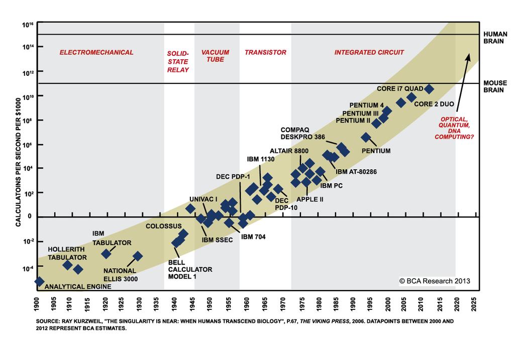
6 Computersciencezone.org Moore s Law 6

7 Reports of my death were greatly exaggerated 7 "In my 34 years in the semiconductor industry, I have witnessed the advertised death of Moore s Law no less than four times. As we progress from 14 nanometer technology to 10 nanometer and plan for 7 nanometer and 5 nanometer and even beyond, our plans are proof that Moore s Law is alive and well Bryan Krzanich, CEO Intel, April 2016

8 Technology supporting Moore s Law Courtesy: Intel 8


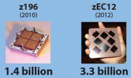
9 Moore s Law Today (2016) Intel Xeon E V4 IBM 7nm Test Chip 14nm Broadwell 22 Cores 2.2 GHz 55MB Cache 416 mm Billion Transistors 456 mm 2 Die size Introduced March 31, nm EUV Photolithography SiGe channels Introduced July

10 10 Evolution in Memory Complexity

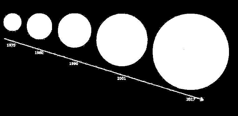
11 Die size (mm) Die Size Growth P6 Pentium proc ~7% growth per year ~2X growth in 10 years Year Apparently, that doesn t apply anymore Die size grows by 14% to satisfy Moore s Law 11 Courtesy, Intel


12 12 Moore was not always accurate


13 Teman s Law ~25 cm ~8 cm 13

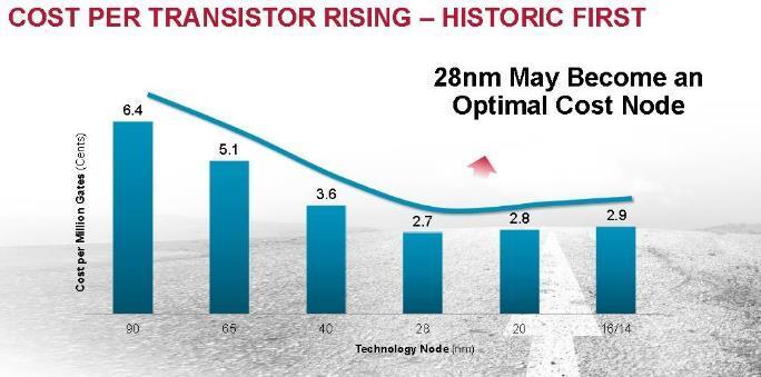

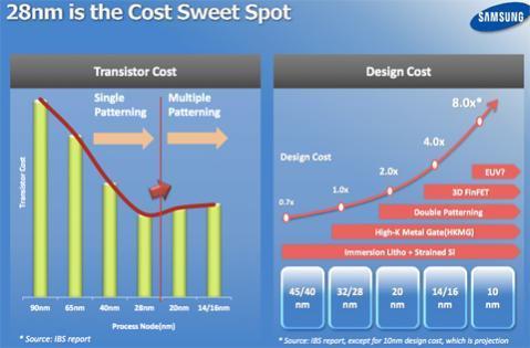
14 14 Cost per Transistor

15 15 Scaling


16 Goals of Technology Scaling Make things cheaper: Want to sell more functions (transistors) per chip for the same money Build same products cheaper, sell the same part for less money Price of a transistor has to be reduced But also want to be faster, smaller, lower power Rabaey s Law of Playstations 16
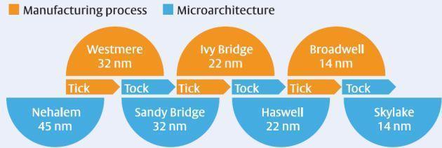
17 Technology Scaling Dennard s Law Benefits of scaling the dimensions by 30% (Dennard): Double transistor density Reduce gate delay by 30% (increase operating frequency by 43%) Reduce energy per transition by 65% (50% power 43% increase in frequency Die size used to increase by 14% per generation Technology generation spans 2-3 years 17
18 1 Moore s Law 2 Scaling Models 3 Current and Future Trends Scaling Models 18


19 Dennard Scaling In 1974, Robert Dennard of IBM described the MOS scaling principles that have accompanied us for forty years. As long as we scale all dimensions of a MOSFET by the same amount (S), we will arrive at better devices and lower cost: L 1/S W 1/S t ox 1/S Na S Vdd 1/S V T 1/S 19
20 Reminder our simple timing/power models In our previous course, we developed the unified model for MOS transistor conduction: 2 I K V V 0.5V 1 V K C I R t ox C W L n ox t ox ox 2 on n GT on V K V DD I R C pd on g on DS GT DSeff DSeff DS V min V, V, V DSeff GT DS DSAT 20 P dyn f C V 2 DD


21 Dennard (Full) Scaling for Long Transistors V L S W S t V V ox DD T N A DSat 1 S S 1 1 S S 1 1 crit L Property Sym Equation Calculation Scaling Good? Oxide Capacitance Device Area Gate Capacitance Transconductance Saturation Current On Resistance Intrinsic Delay Power Power Density C ox A C g K n I on R on t pd P av PD ox t 1 ox Cox 1 S S W L 1 1 S S W L 1 1 S S S C W L 1 1 n ox S S S KV 2 n S S VDD I 1 1 on S S K V V V n DSat GT DSat on GT S S S 1 R C 1 S g f C V DD S S S 2 2 P A S S av 1 S 1 S S 1 S 1 1 S 1 S

22 Dennard Scaling This previous slide showed the principal that has led to scaling for the last 50 years. Assume that we scale our process by 30% every generation S 2 S Therefore, if the area scales by 1/S 2 =1/2, our die size goes down by 2X every generation! In addition, our speed goes up by 30%! And our power also gets cut in half, without any increase in power density. We have hit one of those rare win-win free lunch situations! Sorry I couldn t resist! 22
23 But what if we want more speed? We saw that t C V I pd g DD on We can aggressively increase the speed by keeping the voltage constant. I K V 2 S on n GT 1 2 t S 1 S 1 S pd This led to the Fixed Voltage Scaling Model, which was used until the 1990s (V DD =5V) 23

24 Moore s Law in Frequency 24 Nature
25 Fixed Voltage Scaling V DD L W t V ox T N A 1 S S 1 S S 1 S 1 1 Property Sym Equation Calculation Scaling Good? Oxide Capacitance Device Area Gate Capacitance Transconductance Saturation Current On Resistance Intrinsic Delay Power Power Density C ox A C g K n I on R on t pd P av PD ox t 1 ox Cox 1 S S W L 1 1 S S 1 S W L 1 1 S S S 1 S ncoxw L 1 1 S S S KV n V I 1 S DD on on S S 1 S 2 f C V 2 1 DD S S 1 S Pav 2 GT R C g A S S 1 S 1 1 S S 2 1 S 3 S
26 Fixed Voltage Scaling Short Channel What happens with velocity saturated devices? I on KnVDSat VGT VDSat S S So the on current doesn t increase leading to less effective speed increase. 1 t R C 1 S 1 S pd on g 26 The power density still increases quadratically! DD PD fcv A S S S S

27 Power density (2004 expectation) The Power Density Crisis Patrick Gelsinger, Intel ISSCC

28 What happens as a result of power density? Let s remove the CPU fan 28

29 29 What actually happened?
30 Technology Scaling Models 30 Fixed Voltage Scaling Supply voltages have to be similar for all devices (one battery) Only device dimensions are scaled. 1970s-1990s Full Dennard Scaling (Constant Electrical Field) Scale both device dimensions and voltage by the same factor, S. Electrical fields stay constant, eliminates breakdown and many secondary effects. 1990s-2005 General Scaling Scale device dimensions by S and voltage by U. Now!

31 How about Leakage Power? Later in the semester, we will see that the off current is exponentially dependent on the threshold voltage. VT Ioff In the case of Full Scaling, the leakage current increases exponentially as V T is decreased! e n T Since the 90nm node, static power is one of the major problems in ICs. 31
32 1 Moore s Law 2 Scaling Models 3 Current and Future Trends Current and Future Trends 32

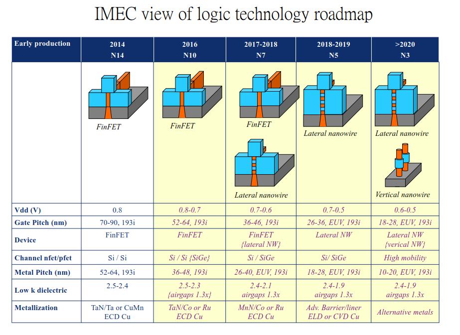
33 ITRS International Technology Roadmap for Semiconductors 33


34 Technology Strategy Roadmap More Moore More than Moore Beyond Moore Quantum Computing 34


35 35 When will Moore s Law End?

36 36 Current Strategies
37 Further Reading J. Rabaey, Digital Integrated Circuits 2003, Chapter 1.3 E. Alon, Berkeley EE-141, Lecture 2 (Fall 2009) a number of years of experience! 37
Lecture 11: MOSFET Modeling
 Digital Integrated Circuits (83-313) Lecture 11: MOSFET ing Semester B, 2016-17 Lecturer: Dr. Adam Teman TAs: Itamar Levi, Robert Giterman 18 June 2017 Disclaimer: This course was prepared, in its entirety,
Lecture 15: Scaling & Economics
 Lecture 15: Scaling & Economics Outline Scaling Transistors Interconnect Future Challenges Economics 2 Moore s Law Recall that Moore s Law has been driving CMOS [Moore65] Corollary: clock speeds have improved
Last Lecture. Power Dissipation CMOS Scaling. EECS 141 S02 Lecture 8
 EECS 141 S02 Lecture 8 Power Dissipation CMOS Scaling Last Lecture CMOS Inverter loading Switching Performance Evaluation Design optimization Inverter Sizing 1 Today CMOS Inverter power dissipation» Dynamic»
Lecture 9: Interconnect
 Digital Integrated Circuits (83-313) Lecture 9: Interconnect Semester B, 2016-17 Lecturer: Dr. Adam Teman TAs: Itamar Levi, Robert Giterman 23 May 2017 Disclaimer: This course was prepared, in its entirety,
Scaling of MOS Circuits. 4. International Technology Roadmap for Semiconductors (ITRS) 6. Scaling factors for device parameters
 6. Scaling factors for device parameters") 1 Scaling of MOS Circuits CONTENTS 1. What is scaling?. Why scaling? 3. Figure(s) of Merit (FoM) for scaling 4. International Technology Roadmap for Semiconductors (ITRS) 5. Scaling models 6. Scaling factors
1 Scaling of MOS Circuits CONTENTS 1. What is scaling?. Why scaling? 3. Figure(s) of Merit (FoM) for scaling 4. International Technology Roadmap for Semiconductors (ITRS) 5. Scaling models 6. Scaling factors
Designing Sequential Logic Circuits
 igital Integrated Circuits (83-313) Lecture 5: esigning Sequential Logic Circuits Semester B, 2016-17 Lecturer: r. Adam Teman TAs: Itamar Levi, Robert Giterman 26 April 2017 isclaimer: This course was
Where Does Power Go in CMOS?
 Power Dissipation Where Does Power Go in CMOS? Dynamic Power Consumption Charging and Discharging Capacitors Short Circuit Currents Short Circuit Path between Supply Rails during Switching Leakage Leaking
CMOS scaling rules Power density issues and challenges Approaches to a solution: Dimension scaling alone Scaling voltages as well
 6.01 - Microelectronic Devices and Circuits Lecture 16 - CMOS scaling; The Roadmap - Outline Announcements PS #9 - Will be due next week Friday; no recitation tomorrow. Postings - CMOS scaling (multiple
HW 5 posted due in two weeks Lab this week Midterm graded Project to be launched in week 7
 HW 5 posted due in two weeks Lab this week Midterm graded Project to be launched in week 7 2 What do digital IC designers need to know? 5 EE4 EECS4 6 3 0< V GS - V T < V DS Pinch-off 7 For (V GS V T )
Practice 3: Semiconductors
 Practice 3: Semiconductors Digital Electronic Circuits Semester A 2012 VLSI Fabrication Process VLSI Very Large Scale Integration The ability to fabricate many devices on a single substrate within a given
The Devices. Digital Integrated Circuits A Design Perspective. Jan M. Rabaey Anantha Chandrakasan Borivoje Nikolic. July 30, 2002
 Digital Integrated Circuits A Design Perspective Jan M. Rabaey Anantha Chandrakasan Borivoje Nikolic The Devices July 30, 2002 Goal of this chapter Present intuitive understanding of device operation Introduction
Digital Integrated Circuits A Design Perspective. Jan M. Rabaey Anantha Chandrakasan Borivoje Nikolic. The Devices. July 30, Devices.
 Digital Integrated Circuits A Design Perspective Jan M. Rabaey Anantha Chandrakasan Borivoje Nikolic The July 30, 2002 1 Goal of this chapter Present intuitive understanding of device operation Introduction
Digital Integrated Circuits (83-313) Lecture 5: Interconnect. Semester B, Lecturer: Adam Teman TAs: Itamar Levi, Robert Giterman 1
 Lecture 5: Interconnect. Semester B, Lecturer: Adam Teman TAs: Itamar Levi, Robert Giterman 1") Digital Integrated Circuits (83-313) Lecture 5: Interconnect Semester B, 2015-16 Lecturer: Adam Teman TAs: Itamar Levi, Robert Giterman 1 What will we learn today? 1 A First Glance at Interconnect 2 3
Digital Integrated Circuits (83-313) Lecture 5: Interconnect Semester B, 2015-16 Lecturer: Adam Teman TAs: Itamar Levi, Robert Giterman 1 What will we learn today? 1 A First Glance at Interconnect 2 3
Today. ESE532: System-on-a-Chip Architecture. Why Care? Message. Scaling. Why Care: Custom SoC
 ESE532: System-on-a-Chip Architecture Day 21: April 5, 2017 VLSI Scaling 1 Today VLSI Scaling Rules Effects Historical/predicted scaling Variations (cheating) Limits Note: gory equations! goal is to understand
Digital Integrated Circuits 2nd Inverter
 Digital Integrated Circuits The Inverter The CMOS Inverter V DD Analysis Inverter complex gate Cost V in V out complexity & Area Integrity and robustness C L Static behavior Performance Dynamic response
CMPEN 411 VLSI Digital Circuits. Lecture 03: MOS Transistor
 CMPEN 411 VLSI Digital Circuits Lecture 03: MOS Transistor Kyusun Choi [Adapted from Rabaey s Digital Integrated Circuits, Second Edition, 2003 J. Rabaey, A. Chandrakasan, B. Nikolic] CMPEN 411 L03 S.1
CMPEN 411 VLSI Digital Circuits. Lecture 04: CMOS Inverter (static view)
") CMPEN 411 VLSI Digital Circuits Lecture 04: CMOS Inverter (static view) Kyusun Choi [Adapted from Rabaey s Digital Integrated Circuits, Second Edition, 2003 J. Rabaey, A. Chandrakasan, B. Nikolic] CMPEN
CMPEN 411 VLSI Digital Circuits Lecture 04: CMOS Inverter (static view) Kyusun Choi [Adapted from Rabaey s Digital Integrated Circuits, Second Edition, 2003 J. Rabaey, A. Chandrakasan, B. Nikolic] CMPEN
Lecture 4: CMOS Transistor Theory
 Introduction to CMOS VLSI Design Lecture 4: CMOS Transistor Theory David Harris, Harvey Mudd College Kartik Mohanram and Steven Levitan University of Pittsburgh Outline q Introduction q MOS Capacitor q
ECE 342 Electronic Circuits. Lecture 6 MOS Transistors
 ECE 342 Electronic Circuits Lecture 6 MOS Transistors Jose E. Schutt-Aine Electrical & Computer Engineering University of Illinois jesa@illinois.edu 1 NMOS Transistor Typically L = 0.1 to 3 m, W = 0.2
Discussions start next week Labs start in week 3 Homework #1 is due next Friday
 EECS141 1 Discussions start next week Labs start in week 3 Homework #1 is due next Friday Everyone should have an EECS instructional account Use cory, quasar, pulsar EECS141 2 1 CMOS LEAKAGE CHARACTERIZATION
Toward More Accurate Scaling Estimates of CMOS Circuits from 180 nm to 22 nm
 Toward More Accurate Scaling Estimates of CMOS Circuits from 180 nm to 22 nm Aaron Stillmaker, Zhibin Xiao, and Bevan Baas VLSI Computation Lab Department of Electrical and Computer Engineering University
Today. ESE534: Computer Organization. Why Care? Why Care. Scaling. ITRS Roadmap
 ESE534: Computer Organization Day 5: September 19, 2016 VLSI Scaling 1 Today VLSI Scaling Rules Effects Historical/predicted scaling Variations (cheating) Limits Note: Day 5 and 6 most gory MOSFET equations
Introduction to CMOS VLSI Design (E158) Lecture 20: Low Power Design
 Lecture 20: Low Power Design") Harris Introduction to CMOS VLSI Design (E158) Lecture 20: Low Power Design David Harris Harvey Mudd College David_Harris@hmc.edu Based on EE271 developed by Mark Horowitz, Stanford University MAH E158
Harris Introduction to CMOS VLSI Design (E158) Lecture 20: Low Power Design David Harris Harvey Mudd College David_Harris@hmc.edu Based on EE271 developed by Mark Horowitz, Stanford University MAH E158
Lecture 28 - The Long Metal-Oxide-Semiconductor Field-Effect Transistor (cont.) April 18, 2007
 April 18, 2007") 6.720J/3.43J - Integrated Microelectronic Devices - Spring 2007 Lecture 28-1 Lecture 28 - The Long Metal-Oxide-Semiconductor Field-Effect Transistor (cont.) April 18, 2007 Contents: 1. Second-order and
6.720J/3.43J - Integrated Microelectronic Devices - Spring 2007 Lecture 28-1 Lecture 28 - The Long Metal-Oxide-Semiconductor Field-Effect Transistor (cont.) April 18, 2007 Contents: 1. Second-order and
EECS 427 Lecture 11: Power and Energy Reading: EECS 427 F09 Lecture Reminders
 EECS 47 Lecture 11: Power and Energy Reading: 5.55 [Adapted from Irwin and Narayanan] 1 Reminders CAD5 is due Wednesday 10/8 You can submit it by Thursday 10/9 at noon Lecture on 11/ will be taught by
Announcements. EE141- Fall 2002 Lecture 7. MOS Capacitances Inverter Delay Power
 - Fall 2002 Lecture 7 MOS Capacitances Inverter Delay Power Announcements Wednesday 12-3pm lab cancelled Lab 4 this week Homework 2 due today at 5pm Homework 3 posted tonight Today s lecture MOS capacitances
Digital Microelectronic Circuits ( ) The CMOS Inverter. Lecture 4: Presented by: Adam Teman
 The CMOS Inverter. Lecture 4: Presented by: Adam Teman") Digital Microelectronic Circuits (361-1-301 ) Presented by: Adam Teman Lecture 4: The CMOS Inverter 1 Last Lectures Moore s Law Terminology» Static Properties» Dynamic Properties» Power The MOSFET Transistor»
Digital Microelectronic Circuits (361-1-301 ) Presented by: Adam Teman Lecture 4: The CMOS Inverter 1 Last Lectures Moore s Law Terminology» Static Properties» Dynamic Properties» Power The MOSFET Transistor»
Lecture 12: Energy and Power. James C. Hoe Department of ECE Carnegie Mellon University
 18 447 Lecture 12: Energy and Power James C. Hoe Department of ECE Carnegie Mellon University 18 447 S18 L12 S1, James C. Hoe, CMU/ECE/CALCM, 2018 Housekeeping Your goal today a working understanding of
EE 330 Lecture 17. MOSFET Modeling CMOS Process Flow
 EE 330 Lecture 17 MOSFET Modeling CMOS Process Flow Review from Last Lecture Limitations of Existing Models V DD V OUT V OUT V DD?? V IN V OUT V IN V IN V DD Switch-Level Models V DD Simple square-law
ECE 305: Fall MOSFET Energy Bands
 ECE 305: Fall 2016 MOSFET Energy Bands Professor Peter Bermel Electrical and Computer Engineering Purdue University, West Lafayette, IN USA pbermel@purdue.edu Pierret, Semiconductor Device Fundamentals
Device Models (PN Diode, MOSFET )
") Device Models (PN Diode, MOSFET ) Instructor: Steven P. Levitan steve@ece.pitt.edu TA: Gayatri Mehta, José Martínez Book: Digital Integrated Circuits: A Design Perspective; Jan Rabaey Lab Notes: Handed
Device Models (PN Diode, MOSFET ) Instructor: Steven P. Levitan steve@ece.pitt.edu TA: Gayatri Mehta, José Martínez Book: Digital Integrated Circuits: A Design Perspective; Jan Rabaey Lab Notes: Handed
EE5311- Digital IC Design
 EE5311- Digital IC Design Module 1 - The Transistor Janakiraman V Assistant Professor Department of Electrical Engineering Indian Institute of Technology Madras Chennai October 28, 2017 Janakiraman, IITM
Nanoscale CMOS Design Issues
 Nanoscale CMOS Design Issues Jaydeep P. Kulkarni Assistant Professor, ECE Department The University of Texas at Austin jaydeep@austin.utexas.edu Fall, 2017, VLSI-1 Class Transistor I-V Review Agenda Non-ideal
Motivation for Lecture. For digital design we use CMOS transistors. Gate Source. CMOS symboler. MOS transistor. Depletion. A channel is created
 Motivation for Lecture igital Integrated ircuits iktor Öwall o see how standard gates are implemented with transistors? How does technology affect the performance, e.g. speed and power consumption? What
The Physical Structure (NMOS)
") The Physical Structure (NMOS) Al SiO2 Field Oxide Gate oxide S n+ Polysilicon Gate Al SiO2 SiO2 D n+ L channel P Substrate Field Oxide contact Metal (S) n+ (G) L W n+ (D) Poly 1 Transistor Resistance Two
The Physical Structure (NMOS) Al SiO2 Field Oxide Gate oxide S n+ Polysilicon Gate Al SiO2 SiO2 D n+ L channel P Substrate Field Oxide contact Metal (S) n+ (G) L W n+ (D) Poly 1 Transistor Resistance Two
Digital Microelectronic Circuits ( ) Ratioed Logic. Lecture 8: Presented by: Mr. Adam Teman
 Ratioed Logic. Lecture 8: Presented by: Mr. Adam Teman") Digital Microelectronic ircuits (361-1-3021 ) Presented by: Mr. Adam Teman Lecture 8: atioed Logic 1 Motivation In the previous lecture, we learned about Standard MOS Digital Logic design. MOS is unquestionably
Digital Microelectronic ircuits (361-1-3021 ) Presented by: Mr. Adam Teman Lecture 8: atioed Logic 1 Motivation In the previous lecture, we learned about Standard MOS Digital Logic design. MOS is unquestionably
EE115C Winter 2017 Digital Electronic Circuits. Lecture 6: Power Consumption
 EE115C Winter 2017 Digital Electronic Circuits Lecture 6: Power Consumption Four Key Design Metrics for Digital ICs Cost of ICs Reliability Speed Power EE115C Winter 2017 2 Power and Energy Challenges
EECS 141: FALL 05 MIDTERM 1
 University of California College of Engineering Department of Electrical Engineering and Computer Sciences D. Markovic TuTh 11-1:3 Thursday, October 6, 6:3-8:pm EECS 141: FALL 5 MIDTERM 1 NAME Last SOLUTION
ECE321 Electronics I
 ECE321 Electronics I Lecture 1: Introduction to Digital Electronics Payman Zarkesh-Ha Office: ECE Bldg. 230B Office hours: Tuesday 2:00-3:00PM or by appointment E-mail: payman@ece.unm.edu Slide: 1 Textbook
ECE 546 Lecture 10 MOS Transistors
 ECE 546 Lecture 10 MOS Transistors Spring 2018 Jose E. Schutt-Aine Electrical & Computer Engineering University of Illinois jesa@illinois.edu NMOS Transistor NMOS Transistor N-Channel MOSFET Built on p-type
Status. Embedded System Design and Synthesis. Power and temperature Definitions. Acoustic phonons. Optic phonons
 Status http://robertdick.org/esds/ Office: EECS 2417-E Department of Electrical Engineering and Computer Science University of Michigan Specification, languages, and modeling Computational complexity,
S=0.7 [0.5x per 2 nodes] ESE370: Circuit-Level Modeling, Design, and Optimization for Digital Systems. Today. Scaling ITRS Roadmap
![S=0.7 [0.5x per 2 nodes] ESE370: Circuit-Level Modeling, Design, and Optimization for Digital Systems. Today. Scaling ITRS Roadmap](/thumbs/92/110446830.jpg "S=0.7 [0.5x per 2 nodes] ESE370: Circuit-Level Modeling, Design, and Optimization for Digital Systems. Today. Scaling ITRS Roadmap") ESE370: Circuit-Level Modeling, Design, and Optimization for Digital Systems Day 15: October 4, 2013 Scaling Today VLSI Scaling Trends/Disciplines Effects Alternatives (cheating) 1 2 Scaling ITRS Roadmap
ESE370: Circuit-Level Modeling, Design, and Optimization for Digital Systems Day 15: October 4, 2013 Scaling Today VLSI Scaling Trends/Disciplines Effects Alternatives (cheating) 1 2 Scaling ITRS Roadmap
CMPEN 411 VLSI Digital Circuits Spring 2012
 CMPEN 411 VLSI Digital Circuits Spring 2012 Lecture 09: Resistance & Inverter Dynamic View [Adapted from Rabaey s Digital Integrated Circuits, Second Edition, 2003 J. Rabaey, A. Chandrakasan, B. Nikolic]
Today s lecture. EE141- Spring 2003 Lecture 4. Design Rules CMOS Inverter MOS Transistor Model
 - Spring 003 Lecture 4 Design Rules CMOS Inverter MOS Transistor Model Today s lecture Design Rules The CMOS inverter at a glance An MOS transistor model for manual analysis Important! Labs start next
CMPEN 411 VLSI Digital Circuits Spring Lecture 14: Designing for Low Power
 CMPEN 411 VLSI Digital Circuits Spring 2012 Lecture 14: Designing for Low Power [Adapted from Rabaey s Digital Integrated Circuits, Second Edition, 2003 J. Rabaey, A. Chandrakasan, B. Nikolic] Sp12 CMPEN
Fig. 1 CMOS Transistor Circuits (a) Inverter Out = NOT In, (b) NOR-gate C = NOT (A or B)
 Inverter Out = NOT In, (b) NOR-gate C = NOT (A or B)") 1 Introduction to Transistor-Level Logic Circuits 1 By Prawat Nagvajara At the transistor level of logic circuits, transistors operate as switches with the logic variables controlling the open or closed
1 Introduction to Transistor-Level Logic Circuits 1 By Prawat Nagvajara At the transistor level of logic circuits, transistors operate as switches with the logic variables controlling the open or closed
EE 466/586 VLSI Design. Partha Pande School of EECS Washington State University
 EE 466/586 VLSI Design Partha Pande School of EECS Washington State University pande@eecs.wsu.edu Lecture 8 Power Dissipation in CMOS Gates Power in CMOS gates Dynamic Power Capacitance switching Crowbar
Lecture 11: J-FET and MOSFET
 ENE 311 Lecture 11: J-FET and MOSFET FETs vs. BJTs Similarities: Amplifiers Switching devices Impedance matching circuits Differences: FETs are voltage controlled devices. BJTs are current controlled devices.
CMOS INVERTER. Last Lecture. Metrics for qualifying digital circuits. »Cost» Reliability» Speed (delay)»performance
»performance") CMOS INVERTER Last Lecture Metrics for qualifying digital circuits»cost» Reliability» Speed (delay)»performance 1 Today s lecture The CMOS inverter at a glance An MOS transistor model for manual analysis
CMOS INVERTER Last Lecture Metrics for qualifying digital circuits»cost» Reliability» Speed (delay)»performance 1 Today s lecture The CMOS inverter at a glance An MOS transistor model for manual analysis
! VLSI Scaling Trends/Disciplines. ! Effects. ! Alternatives (cheating) " Try to predict where industry going
 Try to predict where industry going") ESE370: Circuit-Level Modeling, Design, and Optimization for Digital Systems Today! VLSI Scaling Trends/Disciplines! Effects! Alternatives (cheating) Lec 12: October 4, 2017 Scaling 2 Scaling! Premise:
ESE370: Circuit-Level Modeling, Design, and Optimization for Digital Systems Today! VLSI Scaling Trends/Disciplines! Effects! Alternatives (cheating) Lec 12: October 4, 2017 Scaling 2 Scaling! Premise:
EEC 118 Lecture #2: MOSFET Structure and Basic Operation. Rajeevan Amirtharajah University of California, Davis Jeff Parkhurst Intel Corporation
 EEC 118 Lecture #2: MOSFET Structure and Basic Operation Rajeevan Amirtharajah University of California, Davis Jeff Parkhurst Intel Corporation Announcements Lab 1 this week, report due next week Bring
EE 330 Lecture 16. Devices in Semiconductor Processes. MOS Transistors
 EE 330 Lecture 16 Devices in Semiconductor Processes MOS Transistors Review from Last Time Model Summary I D I V DS V S I B V BS = 0 0 VS VT W VDS ID = μcox VS VT VDS VS V VDS VS VT L T < W μc ( V V )
ESE370: Circuit-Level Modeling, Design, and Optimization for Digital Systems
 ESE370: Circuit-Level Modeling, Design, and Optimization for Digital Systems Lec 12: October 4, 2017 Scaling Penn ESE 370 Fall 2017 - Khanna Today! VLSI Scaling Trends/Disciplines! Effects! Alternatives
Device Models (PN Diode, MOSFET )
") Device Models (PN Diode, MOSFET ) Instructor: Steven P. Levitan steve@ece.pitt.edu TA: Gayatri Mehta, José Martínez Book: Digital Integrated Circuits: A Design Perspective; Jan Rabaey Lab Notes: Handed
Device Models (PN Diode, MOSFET ) Instructor: Steven P. Levitan steve@ece.pitt.edu TA: Gayatri Mehta, José Martínez Book: Digital Integrated Circuits: A Design Perspective; Jan Rabaey Lab Notes: Handed
MOS Transistor Theory
 MOS Transistor Theory So far, we have viewed a MOS transistor as an ideal switch (digital operation) Reality: less than ideal EE 261 Krish Chakrabarty 1 Introduction So far, we have treated transistors
FLCC Seminar. Spacer Lithography for Reduced Variability in MOSFET Performance
 1 Seminar Spacer Lithography for Reduced Variability in MOSFET Performance Prof. Tsu-Jae King Liu Electrical Engineering & Computer Sciences Dept. University of California at Berkeley Graduate Student:
Digital Microelectronic Circuits ( ) Logical Effort. Lecture 7: Presented by: Adam Teman
 Logical Effort. Lecture 7: Presented by: Adam Teman") Digital Microelectronic ircuits (361-1-3021 ) Presented by: Adam Teman Lecture 7: Logical Effort Digital Microelectronic ircuits The VLSI Systems enter - BGU Lecture 7: Logical Effort 1 Last Lectures The
Digital Microelectronic ircuits (361-1-3021 ) Presented by: Adam Teman Lecture 7: Logical Effort Digital Microelectronic ircuits The VLSI Systems enter - BGU Lecture 7: Logical Effort 1 Last Lectures The
MOS Transistor Properties Review
 MOS Transistor Properties Review 1 VLSI Chip Manufacturing Process Photolithography: transfer of mask patterns to the chip Diffusion or ion implantation: selective doping of Si substrate Oxidation: SiO
Lecture 13 MOSFET as an amplifier with an introduction to MOSFET small-signal model and small-signal schematics. Lena Peterson
 Lecture 13 MOSFET as an amplifier with an introduction to MOSFET small-signal model and small-signal schematics Lena Peterson 2015-10-13 Outline (1) Why is the CMOS inverter gain not infinite? Large-signal
CIS 371 Computer Organization and Design
 CIS 371 Computer Organization and Design Unit 13: Power & Energy Slides developed by Milo Mar0n & Amir Roth at the University of Pennsylvania with sources that included University of Wisconsin slides by
τ gd =Q/I=(CV)/I I d,sat =(µc OX /2)(W/L)(V gs -V TH ) 2 ESE534 Computer Organization Today At Issue Preclass 1 Energy and Delay Tradeoff
/I I d,sat =(µc OX /2)(W/L)(V gs -V TH ) 2 ESE534 Computer Organization Today At Issue Preclass 1 Energy and Delay Tradeoff") ESE534 Computer Organization Today Day 8: February 10, 2010 Energy, Power, Reliability Energy Tradeoffs? Voltage limits and leakage? Variations Transients Thermodynamics meets Information Theory (brief,
ESE534 Computer Organization Today Day 8: February 10, 2010 Energy, Power, Reliability Energy Tradeoffs? Voltage limits and leakage? Variations Transients Thermodynamics meets Information Theory (brief,
EE895KR. Advanced VLSI Design
 EE895KR Advanced VLSI Design Kaushik Roy Purdue University Dept. of ECE kaushik@purdue.edu Course Overview Targeted for graduate students who have already taken basic VLSI design classes Real world challenges
ESE 570: Digital Integrated Circuits and VLSI Fundamentals
 ESE 570: Digital Integrated Circuits and VLSI Fundamentals Lec 15: March 15, 2018 Euler Paths, Energy Basics and Optimization Midterm! Midterm " Mean: 89.7 " Standard Dev: 8.12 2 Lecture Outline! Euler
Lecture 6 Power Zhuo Feng. Z. Feng MTU EE4800 CMOS Digital IC Design & Analysis 2010
 EE4800 CMOS Digital IC Design & Analysis Lecture 6 Power Zhuo Feng 6.1 Outline Power and Energy Dynamic Power Static Power 6.2 Power and Energy Power is drawn from a voltage source attached to the V DD
Design for Manufacturability and Power Estimation. Physical issues verification (DSM)
") Design for Manufacturability and Power Estimation Lecture 25 Alessandra Nardi Thanks to Prof. Jan Rabaey and Prof. K. Keutzer Physical issues verification (DSM) Interconnects Signal Integrity P/G integrity
Design for Manufacturability and Power Estimation Lecture 25 Alessandra Nardi Thanks to Prof. Jan Rabaey and Prof. K. Keutzer Physical issues verification (DSM) Interconnects Signal Integrity P/G integrity
MOSFET: Introduction
 E&CE 437 Integrated VLSI Systems MOS Transistor 1 of 30 MOSFET: Introduction Metal oxide semiconductor field effect transistor (MOSFET) or MOS is widely used for implementing digital designs Its major
Impact of Scaling on The Effectiveness of Dynamic Power Reduction Schemes
 Impact of Scaling on The Effectiveness of Dynamic Power Reduction Schemes D. Duarte Intel Corporation david.e.duarte@intel.com N. Vijaykrishnan, M.J. Irwin, H-S Kim Department of CSE, Penn State University
MOS Transistor I-V Characteristics and Parasitics
 ECEN454 Digital Integrated Circuit Design MOS Transistor I-V Characteristics and Parasitics ECEN 454 Facts about Transistors So far, we have treated transistors as ideal switches An ON transistor passes
Lecture 10 MOSFET (III) MOSFET Equivalent Circuit Models
 MOSFET Equivalent Circuit Models") Lecture 10 MOSFET (III) MOSFET Equivalent Circuit Models Outline Lowfrequency smallsignal equivalent circuit model Highfrequency smallsignal equivalent circuit model Reading Assignment: Howe and Sodini;
Lecture 10 MOSFET (III) MOSFET Equivalent Circuit Models Outline Lowfrequency smallsignal equivalent circuit model Highfrequency smallsignal equivalent circuit model Reading Assignment: Howe and Sodini;
CMOS Scaling. Two motivations to scale down. Faster transistors, both digital and analog. To pack more functionality per area. Lower the cost!
 Two motivations to scale down CMOS Scaling Faster transistors, both digital and analog To pack more functionality per area. Lower the cost! (which makes (some) physical sense) Scale all dimensions and
CHAPTER 5 EFFECT OF GATE ELECTRODE WORK FUNCTION VARIATION ON DC AND AC PARAMETERS IN CONVENTIONAL AND JUNCTIONLESS FINFETS
 98 CHAPTER 5 EFFECT OF GATE ELECTRODE WORK FUNCTION VARIATION ON DC AND AC PARAMETERS IN CONVENTIONAL AND JUNCTIONLESS FINFETS In this chapter, the effect of gate electrode work function variation on DC
Midterm. ESE 570: Digital Integrated Circuits and VLSI Fundamentals. Lecture Outline. Pass Transistor Logic. Restore Output.
 ESE 570: Digital Integrated Circuits and VLSI Fundamentals Lec 16: March 21, 2017 Transmission Gates, Euler Paths, Energy Basics Review Midterm! Midterm " Mean: 79.5 " Standard Dev: 14.5 2 Lecture Outline!
From Physics to Logic
 From Physics to Logic This course aims to introduce you to the layers of abstraction of modern computer systems. We won t spend much time below the level of bits, bytes, words, and functional units, but
MOS Transistors. Prof. Krishna Saraswat. Department of Electrical Engineering Stanford University Stanford, CA
 MOS Transistors Prof. Krishna Saraswat Department of Electrical Engineering S Stanford, CA 94305 saraswat@stanford.edu 1 1930: Patent on the Field-Effect Transistor! Julius Lilienfeld filed a patent describing
EE 230 Lecture 31. THE MOS TRANSISTOR Model Simplifcations THE Bipolar Junction TRANSISTOR
 EE 23 Lecture 3 THE MOS TRANSISTOR Model Simplifcations THE Bipolar Junction TRANSISTOR Quiz 3 Determine I X. Assume W=u, L=2u, V T =V, uc OX = - 4 A/V 2, λ= And the number is? 3 8 5 2? 6 4 9 7 Quiz 3
1 cover it in more detail right away, 2 indicate when it will be covered in detail, or. 3 invite you to office hours.
 14 1 8 6 IBM ES9 Bipolar Fujitsu VP IBM 39S Pulsar 4 IBM 39 IBM RY6 CDC Cyber 5 IBM 4381 IBM RY4 IBM 381 Apache Fujitsu M38 IBM 37 Merced IBM 36 IBM 333 Vacuum Pentium II(DSIP) 195 196 197 198 199 NTT
ECE 438: Digital Integrated Circuits Assignment #4 Solution The Inverter
 ECE 438: Digital Integrated Circuits Assignment #4 The Inverter Text: Chapter 5, Digital Integrated Circuits 2 nd Ed, Rabaey 1) Consider the CMOS inverter circuit in Figure P1 with the following parameters.
Lecture 5: CMOS Transistor Theory
 Lecture 5: CMOS Transistor Theory Slides courtesy of Deming Chen Slides based on the initial set from David Harris CMOS VLSI Design Outline q q q q q q q Introduction MOS Capacitor nmos I-V Characteristics
Power Dissipation. Where Does Power Go in CMOS?
 Power Dissipation [Adapted from Chapter 5 of Digital Integrated Circuits, 2003, J. Rabaey et al.] Where Does Power Go in CMOS? Dynamic Power Consumption Charging and Discharging Capacitors Short Circuit
CSE493/593. Designing for Low Power
 CSE493/593 Designing for Low Power Mary Jane Irwin [Adapted from Rabaey s Digital Integrated Circuits, 2002, J. Rabaey et al.].1 Why Power Matters Packaging costs Power supply rail design Chip and system
Nanometer Transistors and Their Models. Jan M. Rabaey
 Nanometer Transistors and Their Models Jan M. Rabaey Chapter Outline Nanometer transistor behavior and models Sub-threshold currents and leakage Variability Device and technology innovations Nanometer
ENGR890 Digital VLSI Design Fall Lecture 4: CMOS Inverter (static view)
") ENGR89 Digital VLSI Design Fall 5 Lecture 4: CMOS Inverter (static view) [Adapted from Chapter 5 of Digital Integrated Circuits, 3, J. Rabaey et al.] [Also borrowed from Vijay Narayanan and Mary Jane Irwin]
ENGR89 Digital VLSI Design Fall 5 Lecture 4: CMOS Inverter (static view) [Adapted from Chapter 5 of Digital Integrated Circuits, 3, J. Rabaey et al.] [Also borrowed from Vijay Narayanan and Mary Jane Irwin]
ESE570 Spring University of Pennsylvania Department of Electrical and System Engineering Digital Integrated Cicruits AND VLSI Fundamentals
 University of Pennsylvania Department of Electrical and System Engineering Digital Integrated Cicruits AND VLSI Fundamentals ESE570, Spring 2018 Final Monday, Apr 0 5 Problems with point weightings shown.
Dual N-/Dual P-Channel 30-V (D-S) MOSFETs
 MOSFETs") Dual N-/Dual P-Channel 3-V (D-S) MOSFETs V (BR)DSS Min (V) r DS(on) Max ( ) V GS(th) (V) I D (A) N-Channel 3 @ V GS = 2 V.8 to 2.5.85 P-Channel 3 2 @ V GS = 2 V 2 to 4.5.6 Low On-Resistance:.8/.6 Low Threshold:.5/
Dual N-/Dual P-Channel 3-V (D-S) MOSFETs V (BR)DSS Min (V) r DS(on) Max ( ) V GS(th) (V) I D (A) N-Channel 3 @ V GS = 2 V.8 to 2.5.85 P-Channel 3 2 @ V GS = 2 V 2 to 4.5.6 Low On-Resistance:.8/.6 Low Threshold:.5/
CMOS Inverter (static view)
") Review: Design Abstraction Levels SYSTEM CMOS Inverter (static view) + MODULE GATE [Adapted from Chapter 5. 5.3 CIRCUIT of G DEVICE Rabaey s Digital Integrated Circuits,, J. Rabaey et al.] S D Review:
Review: Design Abstraction Levels SYSTEM CMOS Inverter (static view) + MODULE GATE [Adapted from Chapter 5. 5.3 CIRCUIT of G DEVICE Rabaey s Digital Integrated Circuits,, J. Rabaey et al.] S D Review:
ECE-305: Spring 2016 MOSFET IV
 ECE-305: Spring 2016 MOSFET IV Professor Mark Lundstrom Electrical and Computer Engineering Purdue University, West Lafayette, IN USA lundstro@purdue.edu Lundstrom s lecture notes: Lecture 4 4/7/16 outline
Lecture 12 CMOS Delay & Transient Response
 EE 471: Transport Phenomena in Solid State Devices Spring 2018 Lecture 12 CMOS Delay & Transient Response Bryan Ackland Department of Electrical and Computer Engineering Stevens Institute of Technology
Lecture #39. Transistor Scaling
 Lecture #39 ANNOUNCEMENT Pick up graded HW assignments and exams (78 Cory) Lecture #40 will be the last formal lecture. Class on Friday will be dedicated to a course review (with sample problems). Discussion
L ECE 4211 UConn F. Jain Scaling Laws for NanoFETs Chapter 10 Logic Gate Scaling
 L13 04202017 ECE 4211 UConn F. Jain Scaling Laws for NanoFETs Chapter 10 Logic Gate Scaling Scaling laws: Generalized scaling (GS) p. 610 Design steps p.613 Nanotransistor issues (page 626) Degradation
EEC 118 Lecture #6: CMOS Logic. Rajeevan Amirtharajah University of California, Davis Jeff Parkhurst Intel Corporation
 EEC 118 Lecture #6: CMOS Logic Rajeevan mirtharajah University of California, Davis Jeff Parkhurst Intel Corporation nnouncements Quiz 1 today! Lab 2 reports due this week Lab 3 this week HW 3 due this
ECE520 VLSI Design. Lecture 23: SRAM & DRAM Memories. Payman Zarkesh-Ha
 ECE520 VLSI Design Lecture 23: SRAM & DRAM Memories Payman Zarkesh-Ha Office: ECE Bldg. 230B Office hours: Wednesday 2:00-3:00PM or by appointment E-mail: pzarkesh@unm.edu Slide: 1 Review of Last Lecture
THE INVERTER. Inverter
 THE INVERTER DIGITAL GATES Fundamental Parameters Functionality Reliability, Robustness Area Performance» Speed (delay)» Power Consumption» Energy Noise in Digital Integrated Circuits v(t) V DD i(t) (a)
ESE 570: Digital Integrated Circuits and VLSI Fundamentals
 ESE 570: Digital Integrated Circuits and VLSI Fundamentals Lec 21: April 4, 2017 Memory Overview, Memory Core Cells Penn ESE 570 Spring 2017 Khanna Today! Memory " Classification " ROM Memories " RAM Memory
Lecture 29 - The Long Metal-Oxide-Semiconductor Field-Effect Transistor (cont.) April 20, 2007
 April 20, 2007") 6.720J/3.43J - Integrated Microelectronic Devices - Spring 2007 Lecture 29-1 Lecture 29 - The Long Metal-Oxide-Semiconductor Field-Effect Transistor (cont.) April 20, 2007 Contents: 1. Non-ideal and second-order
6.720J/3.43J - Integrated Microelectronic Devices - Spring 2007 Lecture 29-1 Lecture 29 - The Long Metal-Oxide-Semiconductor Field-Effect Transistor (cont.) April 20, 2007 Contents: 1. Non-ideal and second-order
EECS130 Integrated Circuit Devices
 EECS130 Integrated Circuit Devices Professor Ali Javey 10/30/2007 MOSFETs Lecture 4 Reading: Chapter 17, 19 Announcements The next HW set is due on Thursday. Midterm 2 is next week!!!! Threshold and Subthreshold
EECS240 Spring Today s Lecture. Lecture 2: CMOS Technology and Passive Devices. Lingkai Kong EECS. EE240 CMOS Technology
 EECS240 Spring 2013 Lecture 2: CMOS Technology and Passive Devices Lingkai Kong EECS Today s Lecture EE240 CMOS Technology Passive devices Motivation Resistors Capacitors (Inductors) Next time: MOS transistor
Chapter 2 Process Variability. Overview. 2.1 Sources and Types of Variations
 Chapter 2 Process Variability Overview Parameter variability has always been an issue in integrated circuits. However, comparing with the size of devices, it is relatively increasing with technology evolution,
Future trends in radiation hard electronics
 Future trends in radiation hard electronics F. Faccio CERN, Geneva, Switzerland Outline Radiation effects in CMOS technologies Deep submicron CMOS for radiation environments What is the future going to
EE 466/586 VLSI Design. Partha Pande School of EECS Washington State University
 EE 466/586 VLSI Design Partha Pande School of EECS Washington State University pande@eecs.wsu.edu Lecture 9 Propagation delay Power and delay Tradeoffs Follow board notes Propagation Delay Switching Time
ECE 497 JS Lecture - 12 Device Technologies
 ECE 497 JS Lecture - 12 Device Technologies Spring 2004 Jose E. Schutt-Aine Electrical & Computer Engineering University of Illinois jose@emlab.uiuc.edu 1 NMOS Transistor 2 ρ Source channel charge density