SOLUTION. Homework 1. Part(a) Due: 15 Mar, 2018, 11:55pm
|
|
|
- Hubert Pierce
- 5 years ago
- Views:
Transcription
1 ENGG1203: Introduction to Electrical and Electronic Engineering Second Semester, Homework 1 Due: 15 Mar, 2018, 11:55pm Instruction: Submit your answers electronically through Moodle. In Moodle, you must submit under the Homework 1 link with the following files: 1. amon.circ for Question 3; 2. ONE (1) PDF file containing answers to all remaining questions Your homework will be graded electronically so you must submit your work as a PDF file. To generate PDF file from your computer, you may use one of the many free PDF creators available, e.g. PDFCreator ( CutePDF Writer ( CutePDF/Writer.asp). You need to design your circuit in Logisim for Question 3. Logisim can be downloaded freely from It runs on Linux, Mac, and Windows machines. Question 1 Part(a) Short Questions Simplify each of the following Boolean expressions by using K-map. Show the completed K-map and the way you looped the 1 s. Furthermore, based on your K-map, implement the expression using only 2-input AND gates, 2-input OR gates, or NOT gates. 1. Z + XY
 (P + Q) 3.")
 r1.")
2 2. P Q + (S Q + R S) (P + Q) 3. (A B + C) (A + C) r1.2 Page 2 of 21

3 r1.2 Page 3 of 21
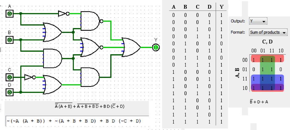
4 Part(b) Any combinational circuit can be represented either with a circuit schematic, a Boolean expression, or a truth table. In the following, you are given one representation of a circuit. Your task is to also represent the same circuit with the other 2 representations. In all cases, inputs are A, B, C, and D, while output is always labeled as Y. Simplify your answer and write Boolean expressions in canonical SOP form. A B C D (i) (ii) Y = AB + B C D + AD + C D (iii) A B C D Y (v) Y A B C (AC + B D) AD + BC + B C D D (iv) A B C D Y (vi) Y r1.2 Page 4 of 21


5 (i) r1.2 Page 5 of 21

6 (ii) r1.2 Page 6 of 21

7 (iii) r1.2 Page 7 of 21

8 (iv) r1.2 Page 8 of 21

9 (v) (vi) r1.2 Page 9 of 21
10 Part(c) The following FSM implements a sequence detector that examines input X, which is a string of 0 s and 1 s, and generates an output Y, which gives a value of 1 when the pattern 010 is detected, and 0 otherwise. The position of Y = 1 coincides with the last 1 detected in the pattern. For example: X = Y = Complete the following state machine such that it will correctly implement this sequence detector. The transitions are labeled with the notation input / [output]. Part(d) 1/[0] 0/[1] 0/[0] 1/[0] S0 S1 S2 1/[0] 0/[0] Draw the timing diagram of the following circuit: A clk B D C Y r1.2 Page 10 of 21
11 A B C D Y clk r1.2 Page 11 of 21
12 Question 2 Complex Number Arithmetic You would like to design a multiplier that multiplies two complex numbers. Let j = 1; engineers like to use j instead of i because the latter is traditionally reserved to denote electric current. Let the two inputs be a + jb and c + jd, then your multiplier produces a complex number e + jf such that e + jf = (a + jb) (c + jd) and e = ac bd (1a) { f = ad + bc (1b) To simplify the design, the complex numbers in your system have only limited range: For all complex numbers x + jy in the system, x, y { 1, 0, 1}. Therefore, for example, 1 + j and j are both valid numbers while 2 + j is not. In your hardware system, each complex number is represented by 4 bits, with 2 bits representing the real part (x of x + jy) in 2 s complement, and 2 bits representing the complex part (y of x + jy) in 2 s complement. Part(a) Real Number Multipliers The first step in your design is to implement a real number multiplier (rm) that you will use to implement equation 1a and 1b. rm takes two 2-bit inputs m (m1m0) and n (n1n0) and produces a 2-bit output p (p1p0). Some examples on how it should behave: m n = p 1 0 = = = 1 r1.2 Page 12 of 21
13 Complete the following truth tables for rm relating p1 p0 to the input m1 m0 n1 n0. Remember: the numbers m, n, p are all encoded as 2-bit 2 s-complement numbers. m1 m0 n1 n0 p1 p r1.2 Page 13 of 21
14 Part(b) K-map and Minimization Based on your answer from the previous part, perform the following: 1. Draw the K-map for the signal p1; 2. Derive the minimized Boolean expression for p1 using the above K-map; 3. Express your answer in canonical SOP form. Part(c) Adder/Subtractor m1, m0 n1, n x x x x x x x m1 m0 n1 + m1 n1 n0 Another component needed to implement equation 1a and 1b is a real value adder/subtractor (ras). Recall that in your system real numbers only take the values of { 1, 0, 1}. If the result of an add or subtract is 2 or 2, then the result will wrap back to 0. For example: = = = ( 1) = 0 The design of ras has 5 input signals and 2 output signals with the following meanings: Direction Name Description input 1 to perform subtraction, 0 to perform issub addition input s1 s0 2-bit input value in 2 s complement input t1 t0 2-bit input value in 2 s complement output r1 r0 2-bit output value in 2 s complement Complete the following truth table for ras: r1.2 Page 14 of 21
15 issub s1 s0 t1 t0 r1 r Part(d) Putting it Together In the following space, draw the design of your complex number multiplier (cm) using the real number multiplier (rm) and the real number adder/subtractor (ras) you designed above as components. Write 1 or 0 if you need to pas a constant 1 or 0 to the circuit. r1.2 Page 15 of 21
16 d1d0 c1c0 b1b0 a1a0 n1n0 p1p0 m1m0 rm n1n0 p1p0 m1m0 rm n1n0 m1m0 n1n0 m1m0 rm rm p1p0 p1p0 0 issub t1t0 s1s0 t1t0 s1s0 issub ras 1 ras r1r0 r1r0 f1f0 e1e0 r1.2 Page 16 of 21


17 Question 3 Alfred the Smart Home Butler You are the chief architecture for Alfred, your company s next flagship product that acts as a voicecontrolled smart home speaker. Alfred is a smart speaker that can play music while controlling all parts of your smart home such lighting and air conditioning. It can process natural language and communicates with you with normal voice conversation. To initiate a voice command, you need to draw Alfred s attention by saying one of the following magic phrases: Hello Alfred With the above, you can then ask Alfred questions such as, Hello Alfred, what is the weather today? or Hello Alfred, turn off the light in kitchen please. In this question, you will design Alfred s monitoring logic that constantly listening to the environment for the magic phrases. As an elite ENGG1203 student, you have decided to implement this logic as a finite state machine. Your monitoring module is connected to the rest of the system as follow. microphone h a s timer amon t p f Query Process Figure 1: Overview of the Alfred system, showing the connection between the monitoring module and the rest of the system. As shown in the diagram your monitoring module has the following input and output signals: Dir Name Description input h 1: the word Hello is detected, 0 otherwise a 1: the word Alfred is detected, 0 otherwise t 1: if timer is expired, 0 otherwise f 1: finished processing voice query, 0 otherwise output s 1: start external timer countdown, 0 otherwise p 1: tell voice query module to process voice command, 0 otherwise A note about the operation of Alfred: amon constantly monitor for the phrase Hello Alfred from the environment. If the phrase is detected, it assert the signal p to start the subsequent query process (e.g. What is the time now?). It relies on the external timer to determine the time between whe the word Hello and Alfred are heard. If, for example, it hears Hello but never hear Alfred within certain time as determined by the timer then it should ignore the Hello and go back to sleep. For example, if someone say, amon should not regard it has a wakeup phrase. Hello Peter, are you going to meet Alfred today? To start the timer, amon should set the signal s to 1 for one cycle. After a specific time, the signal t will be set to 1 by the timer for one cycle. If you assert s before the timer expires, it will simply restart the timer from the begining. Once the Query processing module has completed its task, it assert the signal f for one cycle. r1.2 Page 17 of 21
18 Part(a) Your amon FSM, has the following states defined: State Sleep Hello Awake Description Alfred is sleeping, waiting for the command Hello Alfred Alfred is half awake after hearing Hello Alfred is awake after successfully detecting a magic phrase Part(b) h/[0, 0] Sleep f /[0, 0] h/[1, 0] t h a/[0, 0] Awake a /[0, 1] f/[0, f] (h + t) a/[h, 0] Hello You are implementing the above FSM in hardware. You are encoding the states with 2 bits (s2 s1 s0) using the following encoding: State s1 Encoding s0 Sleep 0 0 Hello 0 1 Awake 1 0 Complete the next state and output logic table for your FSM in the following page. situations, write down X in the corresponding space. For don t care r1.2 Page 18 of 21
19 s1 s0 h a t f ns1 ns0 s p Part(c) Implement the above FSM in Logisim. Apart from the I/O described above, your machine should also include a clock input clk, and a reset input clr. The following table summarizes the input/output ports of your state machine. The column Order indicates the order of the pin in the circuit symbol. r1.2 Page 19 of 21
20 Direction Order Name Logisim Type input 1 h Pin 2 a Pin 3 t Pin 4 f Pin 5 clk Pin 6 clr Pin output 1 s Pin 2 p Pin Your circuit will be graded automatically, so it is very important for you to use the exact pin names in the above table in your circuit. Download the file hw1src.zip. You may use the included amon.circ as a template for your design. You may find the file amon-test.circ useful for testing your circuit. Put the two files (amon.circ and amon-test.circ) in the same directory for the file amon-test.circ to run. Save your answer in amon.circ and submit this file via Moodle. Part(d) Optional: Just for Fun Name the comic/movie that may have inspired the product name Alfred. Batman. In the comic/movie Batman, the main character Batman is called Bruce Wayne, who has a smart butler at home named Alfred Pennyworth. r1.2 Page 20 of 21
21 Question 4 Number Systems in Computers Part(a) Represent the numbers 12, -5, 332, -9, -1.25, π in the following formats. Write N/A if the number cannot be represented in that format: (i) 6-bit unsigned number (ii) 7-bit 2 s complement number (iii) 10-bit 1 s complement number (iv) 8-bit sign-magnitude number with 1 as the most significant bit representing a negative number. Number 6-bit unsigned 7-bit 2 s complement 10-bit 1 s complement 8-bit sign-magnitude N/A N/A N/A N/A 9 N/A N/A N/A N/A N/A π N/A N/A N/A N/A Part(b) Perform the calculation if the 9-bit numbers are in the following formats: (i) 9-bit unsigned number; (ii) 9-bit 1 s complement; (iii) 9-bit 2 s complement; (iv) 9-bit sign-magnitude, with a 1 as the most significant bit representing a negative number. Write your answer in the following table. Indicate with N/A if the number cannot be using the specified format. Write your answers in decimal. number 9-bit unsigned 9-bit 1 s complement sign- 9-bit magnitude = = = = Part(c) Convert the following numbers into binary: , , bit 2 s complement Assuming you are using a computer with 8-bit words, and you decide to use 4 bits to store the values on the LEFT of the binary point, and use the remaining 4 bits to store the values on the RIGHT of the binary point, which of the above numbers can be represented in this new format? Cannot be represented because Cannot be represented because HINT: One easy way to convert these decimal fractional numbers is to multiply the number by 2 4 = 16. In binary number system, multiplying a number by 2 s is equivalent to shifting the number to LEFT by s bit. Therefore, the number representation of a number n in the above case is simply the same as the binary reprentation of the number n 2 4 in binary. Try it on the number r1.2 Page 21 of 21
Homework 1. Part(a) Due: 15 Mar, 2018, 11:55pm
 Due: 15 Mar, 2018, 11:55pm") ENGG1203: Introduction to Electrical and Electronic Engineering Second Semester, 2017 18 Homework 1 Due: 15 Mar, 2018, 11:55pm Instruction: Submit your answers electronically through Moodle. In Moodle,
ENGG1203: Introduction to Electrical and Electronic Engineering Second Semester, 2017 18 Homework 1 Due: 15 Mar, 2018, 11:55pm Instruction: Submit your answers electronically through Moodle. In Moodle,
ENGG1015 Homework 1 Question 1. ENGG1015: Homework 1
 ENGG1015 Homework 1 Question 1 ENGG1015: Homework 1 Due: Nov 5, 2012, 11:55pm Instruction: Submit your answers electronically through Moodle (Link to Homework 1). You may type your answers using any text
ENGG1015: Homework 1
 ENGG1015 Homework 1 Question 1 ENGG1015: Homework 1 Due: Nov 5, 2012, 11:55pm Instruction: Submit your answers electronically through Moodle (Link to Homework 1). You may type your answers using any text
ENGG 1203 Tutorial _03 Laboratory 3 Build a ball counter. Lab 3. Lab 3 Gate Timing. Lab 3 Steps in designing a State Machine. Timing diagram of a DFF
 ENGG 1203 Tutorial _03 Laboratory 3 Build a ball counter Timing diagram of a DFF Lab 3 Gate Timing difference timing for difference kind of gate, cost dependence (1) Setup Time = t2-t1 (2) Propagation
ENGG 1203 Tutorial_9 - Review. Boolean Algebra. Simplifying Logic Circuits. Combinational Logic. 1. Combinational & Sequential Logic
 ENGG 1203 Tutorial_9 - Review Boolean Algebra 1. Combinational & Sequential Logic 2. Computer Systems 3. Electronic Circuits 4. Signals, Systems, and Control Remark : Multiple Choice Questions : ** Check
Combinational Logic. By : Ali Mustafa
 Combinational Logic By : Ali Mustafa Contents Adder Subtractor Multiplier Comparator Decoder Encoder Multiplexer How to Analyze any combinational circuit like this? Analysis Procedure To obtain the output
CPE100: Digital Logic Design I
 Professor Brendan Morris, SEB 3216, brendan.morris@unlv.edu CPE100: Digital Logic Design I Final Review http://www.ee.unlv.edu/~b1morris/cpe100/ 2 Logistics Tuesday Dec 12 th 13:00-15:00 (1-3pm) 2 hour
EE 209 Spiral 1 Exam Solutions Name:
 EE 29 Spiral Exam Solutions Name:.) Answer the following questions as True or False a.) A 4-to- multiplexer requires at least 4 select lines: true / false b.) An 8-to- mux and no other logic can be used
Different encodings generate different circuits
 FSM State Encoding Different encodings generate different circuits no easy way to find best encoding with fewest logic gates or shortest propagation delay. Binary encoding: K states need log 2 K bits i.e.,
University of Florida EEL 3701 Summer 2015 Dr. Eric. M. Schwartz Department of Electrical & Computer Engineering Tuesday, 30 June 2015
 University of Florida EEL 3701 Summer 2015 Dr Eric M Schwartz Page 1/13 Exam 1 May the Schwartz be with you! Instructions: Turn off all cell phones and other noise making devices Show all work on the front
ECE/CS 250 Computer Architecture
 ECE/CS 250 Computer Architecture Basics of Logic Design: Boolean Algebra, Logic Gates (Combinational Logic) Tyler Bletsch Duke University Slides are derived from work by Daniel J. Sorin (Duke), Alvy Lebeck
Please read carefully. Good luck & Go Gators!!!
 Page 1/12 Exam 1 May the Schwartz be with you! Instructions: Turn off all cell phones and other noise making devices and put away all electronics Show all work on the front of the test papers Box each
Adders, subtractors comparators, multipliers and other ALU elements
 CSE4: Components and Design Techniques for Digital Systems Adders, subtractors comparators, multipliers and other ALU elements Instructor: Mohsen Imani UC San Diego Slides from: Prof.Tajana Simunic Rosing
3. Complete the following table of equivalent values. Use binary numbers with a sign bit and 7 bits for the value
 EGC22 Digital Logic Fundamental Additional Practice Problems. Complete the following table of equivalent values. Binary. Octal 35.77 33.23.875 29.99 27 9 64 Hexadecimal B.3 D.FD B.4C 2. Calculate the following
EE 209 Logic Cumulative Exam Name:
 EE 209 Logic Cumulative Exam Name: 1.) Answer the following questions as True or False a.) A 4-to-1 multiplexer requires at least 4 select lines: true / false b.) An 8-to-1 mux and no other logi can be
14.1. Unit 14. State Machine Design
 4. Unit 4 State Machine Design 4.2 Outcomes I can create a state diagram to solve a sequential problem I can implement a working state machine given a state diagram STATE MACHINES OVERVIEW 4.3 4.4 Review
Foundations of Computation
 The Australian National University Semester 2, 2018 Research School of Computer Science Tutorial 1 Dirk Pattinson Foundations of Computation The tutorial contains a number of exercises designed for the
CprE 281: Digital Logic
 CprE 281: Digital Logic Instructor: Alexander Stoytchev http://www.ece.iastate.edu/~alexs/classes/ Synchronous Sequential Circuits Basic Design Steps CprE 281: Digital Logic Iowa State University, Ames,
ENGG1015 Homework 3 Question 1. ENGG1015: Homework 3
 ENGG0 Homewor Question ENGG0: Homewor Due: Dec, 0, :pm Instruction: Submit your answers electronically through Moodle (Lin to Homewor ) You may type your answers using any text editor of your choice, or
University of Florida EEL 3701 Fall 2014 Dr. Eric. M. Schwartz Department of Electrical & Computer Engineering Wednesday, 15 October 2014
 Page 1/12 Exam 1 May the Schwartz Instructions: be with you! Turn off all cell phones and other noise making devices and put away all electronics Show all work on the front of the test papers Box each
ECE 250 / CPS 250 Computer Architecture. Basics of Logic Design Boolean Algebra, Logic Gates
 ECE 250 / CPS 250 Computer Architecture Basics of Logic Design Boolean Algebra, Logic Gates Benjamin Lee Slides based on those from Andrew Hilton (Duke), Alvy Lebeck (Duke) Benjamin Lee (Duke), and Amir
Systems I: Computer Organization and Architecture
 Systems I: Computer Organization and Architecture Lecture 6 - Combinational Logic Introduction A combinational circuit consists of input variables, logic gates, and output variables. The logic gates accept
CE1911 LECTURE FSM DESIGN PRACTICE DAY 1
 REVIEW MATERIAL 1. Combinational circuits do not have memory. They calculate instantaneous outputs based only on current inputs. They implement basic arithmetic and logic functions. 2. Sequential circuits
Table of Content. Chapter 11 Dedicated Microprocessors Page 1 of 25
 Chapter 11 Dedicated Microprocessors Page 1 of 25 Table of Content Table of Content... 1 11 Dedicated Microprocessors... 2 11.1 Manual Construction of a Dedicated Microprocessor... 3 11.2 FSM + D Model
UNIT 4 MINTERM AND MAXTERM EXPANSIONS
 UNIT 4 MINTERM AND MAXTERM EXPANSIONS Spring 2 Minterm and Maxterm Expansions 2 Contents Conversion of English sentences to Boolean equations Combinational logic design using a truth table Minterm and
CSE140: Components and Design Techniques for Digital Systems. Midterm Information. Instructor: Mohsen Imani. Sources: TSR, Katz, Boriello & Vahid
 CSE140: Components and Design Techniques for Digital Systems Midterm Information Instructor: Mohsen Imani Midterm Topics In general: everything that was covered in homework 1 and 2 and related lectures,
ECE20B Final Exam, 200 Point Exam Closed Book, Closed Notes, Calculators Not Allowed June 12th, Name
 C20B Final xam, 200 Point xam Closed Book, Closed Notes, Calculators Not llowed June 2th, 2003 Name Guidelines: Please remember to write your name on your bluebook, and when finished, to staple your solutions
Department of Electrical Engineering and Computer Sciences University of California, Berkeley. Final Exam Solutions
 Electrical Engineering 42/00 Summer 202 Instructor: Tony Dear Department of Electrical Engineering and omputer Sciences University of alifornia, Berkeley Final Exam Solutions. Diodes Have apacitance?!?!
Review Problem 1. should be on. door state, false if light should be on when a door is open. v Describe when the dome/interior light of the car
 Review Problem 1 v Describe when the dome/interior light of the car should be on. v DriverDoorOpen = true if lefthand door open v PassDoorOpen = true if righthand door open v LightSwitch = true if light
Written exam with solutions IE Digital Design Friday 21/
 Written exam with solutions IE204-5 Digital Design Friday 2/0 206 09.00-3.00 General Information Examiner: Ingo Sander. Teacher: Kista, William Sandvist tel 08-7904487, Elena Dubrova phone 08-790 4 4 Exam
Adders, subtractors comparators, multipliers and other ALU elements
 CSE4: Components and Design Techniques for Digital Systems Adders, subtractors comparators, multipliers and other ALU elements Adders 2 Circuit Delay Transistors have instrinsic resistance and capacitance
CPE100: Digital Logic Design I
 Professor Brendan Morris, SEB 3216, brendan.morris@unlv.edu CPE100: Digital Logic Design I Midterm02 Review http://www.ee.unlv.edu/~b1morris/cpe100/ 2 Logistics Thursday Nov. 16 th In normal lecture (13:00-14:15)
CMSC 313 Lecture 17. Focus Groups. Announcement: in-class lab Thu 10/30 Homework 3 Questions Circuits for Addition Midterm Exam returned
 Focus Groups CMSC 33 Lecture 7 Need good sample of all types of CS students Mon /7 & Thu /2, 2:3p-2:p & 6:p-7:3p Announcement: in-class lab Thu /3 Homework 3 Questions Circuits for Addition Midterm Exam
ELCT201: DIGITAL LOGIC DESIGN
 ELCT2: DIGITAL LOGIC DESIGN Dr. Eng. Haitham Omran, haitham.omran@guc.edu.eg Dr. Eng. Wassim Alexan, wassim.joseph@guc.edu.eg Lecture 4 Following the slides of Dr. Ahmed H. Madian محرم 439 ه Winter 28
Building a Computer Adder
 Logic Gates are used to translate Boolean logic into circuits. In the abstract it is clear that we can build AND gates that perform the AND function and OR gates that perform the OR function and so on.
Why digital? Overview. Number Systems. Binary to Decimal conversion
 Why digital? Overview It has the following advantages over analog. It can be processed and transmitted efficiently and reliably. It can be stored and retrieved with greater accuracy. Noise level does not
Lecture 8: Sequential Networks and Finite State Machines
 Lecture 8: Sequential Networks and Finite State Machines CSE 140: Components and Design Techniques for Digital Systems Spring 2014 CK Cheng, Diba Mirza Dept. of Computer Science and Engineering University
Department of Electrical Engineering and Computer Sciences University of California, Berkeley. Final Exam: Friday, August 10, 2012
 Electrical Engineering 42/00 Summer 202 Instructor: Tony Dear Department of Electrical Engineering and Computer Sciences University of California, Berkeley Final Exam: Friday, August 0, 202 Last Name:
Synchronous Sequential Circuit Design. Dr. Ehab A. H. AL-Hialy Page 1
 Synchronous Sequential Circuit Design Dr. Ehab A. H. AL-Hialy Page Motivation Analysis of a few simple circuits Generalizes to Synchronous Sequential Circuits (SSC) Outputs are Function of State (and Inputs)
Written reexam with solutions for IE1204/5 Digital Design Monday 14/
 Written reexam with solutions for IE204/5 Digital Design Monday 4/3 206 4.-8. General Information Examiner: Ingo Sander. Teacher: William Sandqvist phone 08-7904487 Exam text does not have to be returned
King Fahd University of Petroleum and Minerals College of Computer Science and Engineering Computer Engineering Department
 King Fahd University of Petroleum and Minerals College of Computer Science and Engineering Computer Engineering Department Page 1 of 13 COE 202: Digital Logic Design (3-0-3) Term 112 (Spring 2012) Final
Chapter 5 Arithmetic Circuits
 Chapter 5 Arithmetic Circuits SKEE2263 Digital Systems Mun im/ismahani/izam {munim@utm.my,e-izam@utm.my,ismahani@fke.utm.my} February 11, 2016 Table of Contents 1 Iterative Designs 2 Adders 3 High-Speed
Outcomes. Spiral 1 / Unit 5. Logic Function Synthesis KARNAUGH MAPS. Karnaugh Maps
 -. -. Spiral / Unit Mark Redekopp Outcomes I know the difference between combinational and sequential logic and can name examples of each. I understand latency, throughput, and at least technique to improve
Spiral 1 / Unit 5. Karnaugh Maps
 -. Spiral / Unit Karnaugh Maps -. Outcomes I know the difference between combinational and sequential logic and can name examples of each. I understand latency, throughput, and at least technique to improve
EEE2135 Digital Logic Design
 EEE2135 Digital Logic Design Chapter 7. Sequential Circuits Design 서강대학교 전자공학과 1. Model of Sequential Circuits 1) Sequential vs. Combinational Circuits a. Sequential circuits: Outputs depend on both the
Digital Logic Design ABC. Representing Logic Operations. Dr. Kenneth Wong. Determining output level from a diagram. Laws of Boolean Algebra
 Digital Logic Design ENGG1015 1 st Semester, 2011 Representing Logic Operations Each function can be represented equivalently in 3 ways: Truth table Boolean logic expression Schematics Truth Table Dr.
Ch 7. Finite State Machines. VII - Finite State Machines Contemporary Logic Design 1
 Ch 7. Finite State Machines VII - Finite State Machines Contemporary Logic esign 1 Finite State Machines Sequential circuits primitive sequential elements combinational logic Models for representing sequential
ENEL Digital Circuits Final Examination
 Name: I#: Lecture Section: ENEL 353 - igital Circuits Final Examination Lecture sections : N. R. Bartley, MWF : :5, ENC 24 2: S. A. Norman, MWF : :5, ST 45 Wednesday, ecember 7, 24 Time: 7: PM : PM Locations:
Read this before starting!
 Points missed: Student's Name: Total score: / points East Tennessee State University epartment of Computer and Information Sciences CSCI 25 (Tarnoff) Computer Organization TEST 2 for Spring Semester, 27
Outcomes. Spiral 1 / Unit 5. Logic Function Synthesis KARNAUGH MAPS. Karnaugh Maps
 -. -. Spiral / Unit Mark Redekopp Outcomes I know the difference between combinational and sequential logic and can name examples of each. I understand latency, throughput, and at least technique to improve
Preparation of Examination Questions and Exercises: Solutions
 Questions Preparation of Examination Questions and Exercises: Solutions. -bit Subtraction: DIF = B - BI B BI BO DIF 2 DIF: B BI 4 6 BI 5 BO: BI BI 4 5 7 3 2 6 7 3 B B B B B DIF = B BI ; B = ( B) BI ( B),
Binary addition example worked out
 Binary addition example worked out Some terms are given here Exercise: what are these numbers equivalent to in decimal? The initial carry in is implicitly 0 1 1 1 0 (Carries) 1 0 1 1 (Augend) + 1 1 1 0
ECE 545 Digital System Design with VHDL Lecture 1A. Digital Logic Refresher Part A Combinational Logic Building Blocks
 ECE 545 Digital System Design with VHDL Lecture A Digital Logic Refresher Part A Combinational Logic Building Blocks Lecture Roadmap Combinational Logic Basic Logic Review Basic Gates De Morgan s Laws
Read this before starting!
 Points missed: Student's Name: Total score: / points East Tennessee State University Department of Computer and Information Sciences CSCI 25 (Tarnoff) Computer Organization TEST 2 for Spring Semester,
ECE/CS 250: Computer Architecture. Basics of Logic Design: Boolean Algebra, Logic Gates. Benjamin Lee
 ECE/CS 250: Computer Architecture Basics of Logic Design: Boolean Algebra, Logic Gates Benjamin Lee Slides based on those from Alvin Lebeck, Daniel Sorin, Andrew Hilton, Amir Roth, Gershon Kedem Admin
Boolean Algebra. Digital Logic Appendix A. Postulates, Identities in Boolean Algebra How can I manipulate expressions?
 Digital Logic Appendix A Gates Combinatorial Circuits Sequential Circuits Other operations NAND A NAND B = NOT ( A ANDB) = AB NOR A NOR B = NOT ( A ORB) = A + B Truth tables What is the result of the operation
Introduction to Karnaugh Maps
 Introduction to Karnaugh Maps Review So far, you (the students) have been introduced to truth tables, and how to derive a Boolean circuit from them. We will do an example. Consider the truth table for
We are here. Assembly Language. Processors Arithmetic Logic Units. Finite State Machines. Circuits Gates. Transistors
 CSC258 Week 3 1 Logistics If you cannot login to MarkUs, email me your UTORID and name. Check lab marks on MarkUs, if it s recorded wrong, contact Larry within a week after the lab. Quiz 1 average: 86%
CE Optimized State Machines
 C 1911 Optimized State Machines Un-used states o we care about un-used states? YS! Start-up Bit errors 2 tj Un-used states Mod 5 counter reset 000 001 010 100 011 101 111 110 3 tj Un-used states Mod 5
Chapter 4. Combinational: Circuits with logic gates whose outputs depend on the present combination of the inputs. elements. Dr.
 Chapter 4 Dr. Panos Nasiopoulos Combinational: Circuits with logic gates whose outputs depend on the present combination of the inputs. Sequential: In addition, they include storage elements Combinational
Written exam for IE1204/5 Digital Design with solutions Thursday 29/
 Written exam for IE4/5 Digital Design with solutions Thursday 9/ 5 9.-. General Information Examiner: Ingo Sander. Teacher: William Sandqvist phone 8-794487 Exam text does not have to be returned when
Parity Checker Example. EECS150 - Digital Design Lecture 9 - Finite State Machines 1. Formal Design Process. Formal Design Process
 Parity Checker Example A string of bits has even parity if the number of 1 s in the string is even. Design a circuit that accepts a bit-serial stream of bits and outputs a 0 if the parity thus far is even
Fundamentals of Digital Design
 Fundamentals of Digital Design Digital Radiation Measurement and Spectroscopy NE/RHP 537 1 Binary Number System The binary numeral system, or base-2 number system, is a numeral system that represents numeric
10/12/2016. An FSM with No Inputs Moves from State to State. ECE 120: Introduction to Computing. Eventually, the States Form a Loop
 University of Illinois at Urbana-Champaign Dept. of Electrical and Computer Engineering An FSM with No Inputs Moves from State to State What happens if an FSM has no inputs? ECE 120: Introduction to Computing
Digital Logic Design - Chapter 5
 Digital Logic Design - Chapter 5 S. Design a 2-bit binary up counter a) using positive-edge-triggered D flip-flops. b) using positive-edge-triggered T flip-flops. c) using positive-edge-triggered JK flip-flops.
Boolean Algebra. Digital Logic Appendix A. Boolean Algebra Other operations. Boolean Algebra. Postulates, Identities in Boolean Algebra
 Digital Logic Appendix A Gates Combinatorial Circuits Sequential Circuits George Boole ideas 1854 Claude Shannon, apply to circuit design, 1938 (piirisuunnittelu) Describe digital circuitry function programming
What s the Deal? MULTIPLICATION. Time to multiply
 What s the Deal? MULTIPLICATION Time to multiply Multiplying two numbers requires a multiply Luckily, in binary that s just an AND gate! 0*0=0, 0*1=0, 1*0=0, 1*1=1 Generate a bunch of partial products
COMBINATIONAL LOGIC FUNCTIONS
 COMBINATIONAL LOGIC FUNCTIONS Digital logic circuits can be classified as either combinational or sequential circuits. A combinational circuit is one where the output at any time depends only on the present
UNIVERSITI TENAGA NASIONAL. College of Information Technology
 UNIVERSITI TENAGA NASIONAL College of Information Technology BACHELOR OF COMPUTER SCIENCE (HONS.) FINAL EXAMINATION SEMESTER 2 2012/2013 DIGITAL SYSTEMS DESIGN (CSNB163) January 2013 Time allowed: 3 hours
Binary addition (1-bit) P Q Y = P + Q Comments Carry = Carry = Carry = Carry = 1 P Q
 P Q Y = P + Q Comments Carry = Carry = Carry = Carry = 1 P Q") Digital Arithmetic In Chapter 2, we have discussed number systems such as binary, hexadecimal, decimal, and octal. We have also discussed sign representation techniques, for example, sign-bit representation
Digital Arithmetic In Chapter 2, we have discussed number systems such as binary, hexadecimal, decimal, and octal. We have also discussed sign representation techniques, for example, sign-bit representation
Finite State Machine (FSM)
") Finite State Machine (FSM) Consists of: State register Stores current state Loads next state at clock edge Combinational logic Computes the next state Computes the outputs S S Next State CLK Current State
Finite State Machine (FSM) Consists of: State register Stores current state Loads next state at clock edge Combinational logic Computes the next state Computes the outputs S S Next State CLK Current State
Name: ID# a) Complete the state transition table for the aforementioned circuit
 Complete the state transition table for the aforementioned circuit") UNIVERSITY OF CALIFORNIA Department of Electrical Engineering and Computer Sciences EECS150 Fall 2001 Prof. Subramanian Final Examination 1) You are to design a sequential circuit with two JK FFs A and
UNIVERSITY OF CALIFORNIA Department of Electrical Engineering and Computer Sciences EECS150 Fall 2001 Prof. Subramanian Final Examination 1) You are to design a sequential circuit with two JK FFs A and
Combina-onal Logic Chapter 4. Topics. Combina-on Circuit 10/13/10. EECE 256 Dr. Sidney Fels Steven Oldridge
 Combina-onal Logic Chapter 4 EECE 256 Dr. Sidney Fels Steven Oldridge Topics Combina-onal circuits Combina-onal analysis Design procedure simple combined to make complex adders, subtractors, converters
211: Computer Architecture Summer 2016
 211: Computer Architecture Summer 2016 Liu Liu Topic: Storage Project3 Digital Logic - Storage: Recap - Review: cache hit rate - Project3 - Digital Logic: - truth table => SOP - simplification: Boolean
DIGITAL LOGIC CIRCUITS
 DIGITAL LOGIC CIRCUITS Digital logic circuits BINARY NUMBER SYSTEM electronic circuits that handle information encoded in binary form (deal with signals that have only two values, and ) Digital. computers,
Simulation of Logic Primitives and Dynamic D-latch with Verilog-XL
 Simulation of Logic Primitives and Dynamic D-latch with Verilog-XL November 30, 2011 Robert D Angelo Tufts University Electrical and Computer Engineering EE-103 Lab 3: Part I&II Professor: Dr. Valencia
ELEC Digital Logic Circuits Fall 2014 Sequential Circuits (Chapter 6) Finite State Machines (Ch. 7-10)
 Finite State Machines (Ch. 7-10)") ELEC 2200-002 Digital Logic Circuits Fall 2014 Sequential Circuits (Chapter 6) Finite State Machines (Ch. 7-10) Vishwani D. Agrawal James J. Danaher Professor Department of Electrical and Computer Engineering
ELEC 2200-002 Digital Logic Circuits Fall 2014 Sequential Circuits (Chapter 6) Finite State Machines (Ch. 7-10) Vishwani D. Agrawal James J. Danaher Professor Department of Electrical and Computer Engineering
From Sequential Circuits to Real Computers
 1 / 36 From Sequential Circuits to Real Computers Lecturer: Guillaume Beslon Original Author: Lionel Morel Computer Science and Information Technologies - INSA Lyon Fall 2017 2 / 36 Introduction What we
Overview. Arithmetic circuits. Binary half adder. Binary full adder. Last lecture PLDs ROMs Tristates Design examples
 Overview rithmetic circuits Last lecture PLDs ROMs Tristates Design examples Today dders Ripple-carry Carry-lookahead Carry-select The conclusion of combinational logic!!! General-purpose building blocks
Review for Test 1 : Ch1 5
 Review for Test 1 : Ch1 5 October 5, 2006 Typeset by FoilTEX Positional Numbers 527.46 10 = (5 10 2 )+(2 10 1 )+(7 10 0 )+(4 10 1 )+(6 10 2 ) 527.46 8 = (5 8 2 ) + (2 8 1 ) + (7 8 0 ) + (4 8 1 ) + (6 8
Looking at a two binary digit sum shows what we need to extend addition to multiple binary digits.
 A Full Adder The half-adder is extremely useful until you want to add more that one binary digit quantities. The slow way to develop a two binary digit adders would be to make a truth table and reduce
Lecture 6: Manipulation of Algebraic Functions, Boolean Algebra, Karnaugh Maps
 EE210: Switching Systems Lecture 6: Manipulation of Algebraic Functions, Boolean Algebra, Karnaugh Maps Prof. YingLi Tian Feb. 21/26, 2019 Department of Electrical Engineering The City College of New York
CSC9R6 Computer Design. Practical Digital Logic
 CSC9R6 Computer Design Practical Digital Logic 1 References (for this part of CSC9R6) Hamacher et al: Computer Organization App A. In library Floyd: Digital Fundamentals Ch 1, 3-6, 8-10 web page: www.prenhall.com/floyd/
1.10 (a) Function of AND, OR, NOT, NAND & NOR Logic gates and their input/output.
 Function of AND, OR, NOT, NAND & NOR Logic gates and their input/output.") Chapter 1.10 Logic Gates 1.10 (a) Function of AND, OR, NOT, NAND & NOR Logic gates and their input/output. Microprocessors are the central hardware that runs computers. There are several components that
Chapter 1.10 Logic Gates 1.10 (a) Function of AND, OR, NOT, NAND & NOR Logic gates and their input/output. Microprocessors are the central hardware that runs computers. There are several components that
Digital Logic Appendix A
 Digital Logic Appendix A Boolean Algebra Gates Combinatorial Circuits Sequential Circuits 1 Boolean Algebra George Boole ideas 1854 Claude Shannon, apply to circuit design, 1938 Describe digital circuitry
Midterm Examination # 1 Wednesday, February 25, Duration of examination: 75 minutes
 Page 1 of 10 School of Computer Science 60-265-01 Computer Architecture and Digital Design Winter 2009 Semester Midterm Examination # 1 Wednesday, February 25, 2009 Student Name: First Name Family Name
Digital Systems and Information Part II
 Digital Systems and Information Part II Overview Arithmetic Operations General Remarks Unsigned and Signed Binary Operations Number representation using Decimal Codes BCD code and Seven-Segment Code Text
9.1. Unit 9. Implementing Combinational Functions with Karnaugh Maps or Memories
 . Unit Implementing Combinational Functions with Karnaugh Maps or Memories . Outcomes I can use Karnaugh maps to synthesize combinational functions with several outputs I can determine the appropriate
Boolean Algebra and Digital Logic 2009, University of Colombo School of Computing
 IT 204 Section 3.0 Boolean Algebra and Digital Logic Boolean Algebra 2 Logic Equations to Truth Tables X = A. B + A. B + AB A B X 0 0 0 0 3 Sum of Products The OR operation performed on the products of
Digital Systems Roberto Muscedere Images 2013 Pearson Education Inc. 1
 Digital Systems Digital systems have such a prominent role in everyday life The digital age The technology around us is ubiquitous, that is we don t even notice it anymore Digital systems are used in:
Review for B33DV2-Digital Design. Digital Design
 Review for B33DV2 The Elements of Modern Behaviours Design Representations Blocks Waveforms Gates Truth Tables Boolean Algebra Switches Rapid Prototyping Technologies Circuit Technologies TTL MOS Simulation
CSE 140 Spring 2017: Final Solutions (Total 50 Points)
") CSE 140 Spring 2017: Final Solutions (Total 50 Points) 1. (Boolean Algebra) Prove the following Boolean theorem using Boolean laws only, i.e. no theorem is allowed for the proof. State the name of the
CSE 140 Spring 2017: Final Solutions (Total 50 Points) 1. (Boolean Algebra) Prove the following Boolean theorem using Boolean laws only, i.e. no theorem is allowed for the proof. State the name of the
State Graphs FSMs. Page 1
 State Graphs FSMs Page 1 Binary Counter State Graph 00 Q1 Q0 N1 N0 0 0 0 1 0 1 1 0 1 0 1 1 1 1 0 0 11 01 State graphs are graphical representations of TT s They contain the same information: no more, no
Digital Electronics Sequential Logic
 /5/27 igital Electronics Sequential Logic r. I. J. Wassell Sequential Logic The logic circuits discussed previously are known as combinational, in that the output depends only on the condition of the latest
ECEN 248: INTRODUCTION TO DIGITAL SYSTEMS DESIGN. Week 2 Dr. Srinivas Shakkottai Dept. of Electrical and Computer Engineering
 ECEN 248: INTRODUCTION TO DIGITAL SYSTEMS DESIGN Week 2 Dr. Srinivas Shakkottai Dept. of Electrical and Computer Engineering Boolean Algebra Boolean Algebra A Boolean algebra is defined with: A set of
7 Multipliers and their VHDL representation
 7 Multipliers and their VHDL representation 7.1 Introduction to arithmetic algorithms If a is a number, then a vector of digits A n 1:0 = [a n 1... a 1 a 0 ] is a numeral representing the number in the
Digital Systems Overview. Unit 1 Numbering Systems. Why Digital Systems? Levels of Design Abstraction. Dissecting Decimal Numbers
 Unit Numbering Systems Fundamentals of Logic Design EE2369 Prof. Eric MacDonald Fall Semester 2003 Digital Systems Overview Digital Systems are Home PC XBOX or Playstation2 Cell phone Network router Data
Philadelphia University Student Name: Student Number:
 Philadelphia University Student Name: Student Number: Faculty of Engineering Serial Number: Final Exam, Second Semester: 2015/2016 Dept. of Computer Engineering Course Title: Logic Circuits Date: 08/06/2016
Digital Techniques. Figure 1: Block diagram of digital computer. Processor or Arithmetic logic unit ALU. Control Unit. Storage or memory unit
 Digital Techniques 1. Binary System The digital computer is the best example of a digital system. A main characteristic of digital system is its ability to manipulate discrete elements of information.
Design of Sequential Circuits
 Design of Sequential Circuits Seven Steps: Construct a state diagram (showing contents of flip flop and inputs with next state) Assign letter variables to each flip flop and each input and output variable