S.E. Sem. III [ETRX] Electronic Circuits and Design I
|
|
|
- Lynne Pitts
- 5 years ago
- Views:
Transcription
![S.E. Sem. [ETRX] Electronic ircuits and Design Time : 3 Hrs.] Prelim Paper Solution [Marks : 80 Q.1(a) What happens when diode is operated at high frequency? [5] Ans.](/docs-images/95/124107626/images/1-0.jpg ": Diode High Frequency Model : This purely resistive A model for the diode works well when the frequency of the A signals is sufficiently low.")
1 S.E. Sem. [ETRX] Electronic ircuits and Design Time : 3 Hrs.] Prelim Paper Solution [Marks : 80 Q.1(a) What happens when diode is operated at high frequency? [5] Ans.: Diode High Frequency Model : This purely resistive A model for the diode works well when the frequency of the A signals is sufficiently low. At high frequencies, we need to include the effects that arise due to these time varying signals and the charge separation that exists in the depletion region and in the ulk p and n regions of the diode under forward ias conditions. Within the device and the depletion region there exists an electric field. For A signals, this electric field is varying with time. As you ve learned in electromagnetics, a time varying electric field is a displacement current. The effects of a displacement current are modeled y equivalent circuit capacitances : We won t do anything with this effect now. This is presented primarily as an FY. Q.1() Explain why configuration is referred as Voltage follower. [5] Ans.: As amplifier provides Av = 1 = Vo. mplies that Vo = Vi, i.e. output follows input, Vi hence the name voltage follower Q.1(c) Draw transfer and drain characteristics of EMOSFET. [5] Ans.: The transfer and drain characteristics of EMOSFET is as shown D (ma) +5 V +3 V +2 V V GS = +1V V DS (V) Q.1(d) Explain construction of Schottky diode and draw its characteristics. [5] Ans.: t is mainly used as a rectifier at signal frequency exceeding 300 MHz due to it s quick response time and lower noise Figure. t has more uniform junction region and is more rugged than PN diode. 1 2 D (ma) DSS 1 V DS constant Drain characteristics V DS (V) V T Transfer characteristics
2 : S.E. ED - onstruction : t is a metalsemiconductor junction diode with no depletion layer. t uses a metal (like gold, silver, platinum, tungsten etc.) on one side of junction and usually an N type doped silicon semiconductor on the other side. The diode construct & its symol are shown in aove Figure. Gold leaf metal contact A node (+) (+) N () Silicon dioxide screen ntype silicon metal Metal semiconductor Metal metal athode () Fig. 1: Schottky Barrier diode (a) asic structure () symol Applications : 1) Because of these quality schottky diode can easily rectify signals of frequencies exceeding 300 MH 3, it can produce an almost perfect half wave rectified output. 2) t is commonly used in switching power supplied that operates at frequencies of 20 GHz. 3) Due to low noise Figure it is extremely important in communication receivers and radar units etc. Fig. 2 : Application of Schottky Barrier diode as rectifier. Q.1(e) What is the Voltage Regulator explain simple zener shunt voltage Regulator. [5] Ans.: A regulator is an electronic circuit that provides constant and stailized output independent of variation of applied input voltage. The Zener Shunt Regulator is as shown. R S The circuit diagram of zener shunt regulator is z as shown. The zener is connected in shunt with the load, and zener is kept reverse iased. The unregulated input V i must e greater than V 0, atleast y 5 to 10 V. The resistor R S will ensure a minimum current through zener when V i = V i min, keeping the zener in ON state. Also it limits the maximum value of zener current when V i = V i max. n the ON state, zener maintains a constant voltage across its terminals. Therefore V 0 = V z. Since V z is a stale zener reference source, the output voltage is stale and hence the load gets a constant voltage. V 0 V t V i V z V 0 R 2
 Draw Energy and diagram of pin junction diode under : (i) Zero Bias, (ii) Forward ias and")
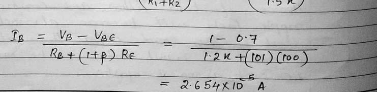
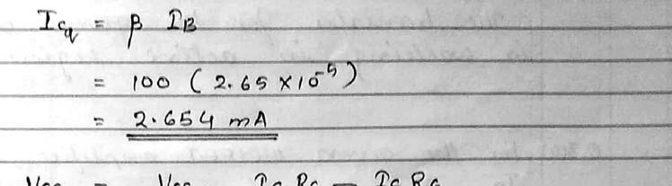
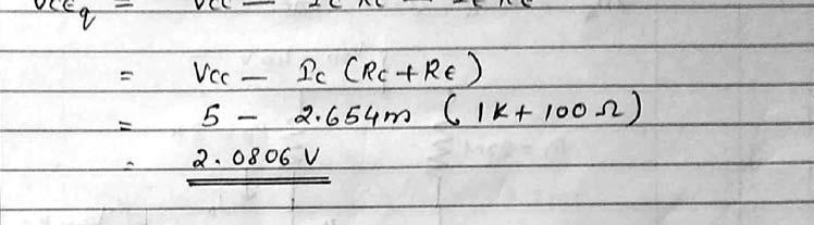
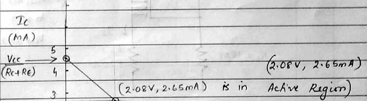
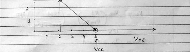
![(iii) Reverse Bias Ans.: (a) zero ias, () reverse ias, and (c) forward ias [10] Q.2() Ans.](/docs-images/95/124107626/images/3-2.jpg ": For the given circuit find Steady State D Parameters cq and V ceq Given = 100 and V BE = 0.")
3 Prelim Paper Solution Q.2(a) Draw Energy and diagram of pin junction diode under : (i) Zero Bias, (ii) Forward ias and (iii) Reverse Bias Ans.: (a) zero ias, () reverse ias, and (c) forward ias [10] Q.2() Ans.: For the given circuit find Steady State D Parameters cq and V ceq Given = 100 and V BE = 0.7 V, also state in which region the circuit is working. 6 K 1.5 K 1 K 5 V 100 ohm [10] 3

4 : S.E. ED - 4


5 Prelim Paper Solution Q.3(a) Ans.: For the given MOSFET amplifier, Determine Dq, V GSq and V DS. R 1 K 22 M R 2 18 M V dd 3 K 40 V R D R s 820 V s D s V GS (Th) = 5 V D (ON) = 3 ma V GS (ON) = 10 V [10] 5

6 : S.E. ED - 6
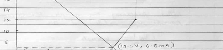
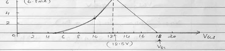
![Prelim Paper Solution Q.3() Explain working principle, characteristics and applications of Tunnel diode. [10] Ans.](/docs-images/95/124107626/images/7-0.jpg ": Tunnel diode is a specially made p-n junction device which exhiits negative resistance over part of the forward ias characteristic.")
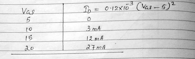
7 Prelim Paper Solution Q.3() Explain working principle, characteristics and applications of Tunnel diode. [10] Ans.: Tunnel diode is a specially made p-n junction device which exhiits negative resistance over part of the forward ias characteristic. t has extremely heavy doping on oth sides of the junction and an arupt transition from the p-side to the n-side. The tunneling effect is a majority carrier effect and is consequently very fast. The tunnel diode is useful for oscillation or amplification purposes. Because of the thin junction and short transit time, it is also useful for microwave applications in fast switching circuits. Volt-amp haracteristics of a Tunnel Diode The volt-ampere characteristics of a tunnel diode are shown in Figure elow. (a) Fig. 1 : (a) Sum of tunneling and injection, () V- characteristic of tunnel diode. The tunnel effect controls the current at very low values of forward ias where the normal or the injection current is very small as shown in Figure aove. The mechanism of tunneling is purely a quantum mechanical phenomenon. An electron on one side of the arrier will have a certain proaility of leaking through the arrier if arrier is very thin. f oth p and n type materials of a junction are heavily doped, the depletion region ecomes very narrow; as narrow as of the order of 100 A. Fig. 2: Symol for tunnel diode Q.4(a) Derive expression for ripple factor for section filter. [10] Ans.:.. Filter : n case of filter the ripple factor is directly proportional to the R, whereas in c Filter, the ripple factor is inversely proportional to R, it means in oth the circuit depends upon the R, to overcome the aove prolem, we use Filter, which is comination of & filter, and in Filter the ripple factor is independent of load resistance R. () 7
8 : S.E. ED - As shown in the figure, the rectifier output is given to the inductor. The inductor provides more opposition to the A component and less opposition to the D component. This results that, most of the A component appears across the inductor and whole of the D component passes to the load. f at all any part part of A component manages to reach the load, then it is removed y the capacitor. Derivation for Ripple Factor : Assumption Mode : i) While otaining the expression for the ripple factor, we will consider only the second harmonics component and neglect all other higher order harmonics. ii) nductive Reactance X > apacitive Reactance X. The Full wave Rectifier output is pulsating in nature, hence its Fourier Series is given as : 2Vm 4Vm 4Vm cos2wt cos4wt 3 15 Neglecting higher order harmonics. 2Vm 4Vm cos2wt 3 2V n the aove equation m represents the d.c. component availale at the output of 4Vm Rectifier and cos2wt represents the A component availale at the Rectifier 3 output. The peak value of the A current is given as : 4Vm cos2wt 3 peak X Assuming cos 2 wt = 1, 4Vm peak 3X RMS D D A D D peak 4Vm 2 3 2X 2 RMS V 3 2X dc 2 2V 3 2X m But 2V m R V dc 8
9 2 V RMS 3 X dc Now the RMS voltage developed across the load is given as : V X RMS RMS 2 Vdc VRMS X 3 X VRMS 2 X V 3 X dc 2 X 3 X where X 1 2w & X 9 2w Prelim Paper Solution Q.4() Derive expression for nput resistance, Voltage gain, current gain and output [10] resistance for E amplifier with R E unypassed. Ans.: ommon Emitter BJT Amplifier with R E unypassed (a) ircuit diagram : V i +V () ac Equivalent circuit : Short V and short all the capacitors (c) Replace transistor y its h parameter model : RB V i R B i 0 h ie Q V i R B R V 0 R R E (1 + h fe ) R E V 0 h fe R i Vi.h ie (1h fe)r R E 0 Q R E1 h (1h )R ie fe E R V 0
10 : S.E. ED - Q.5(a) Ans.: (d) To find input resistance R i = V i / i : Vi Vi.h ie (1h fe)re RB R i =.. R h (1h )R i i B ie fe E = h (1 h )R.R ie fe E B R h (1h )R B ie fe E (e) To find output resistance R 0 : R 0 = R = R h (1h )R B ie fe E (f) To find voltage gain A v = V 0 / V i : Output Voltage (V 0).R 0 A v = = nput Voltage (V ).h (1h )R hfe R = h (1h )R ie fe E i ie fe E hfe R = h (1h )R ie fe E The ve sign indicates that input and output voltages are 180 out of phase. (g) To find current gain A = 0 / i output current A i = input current = 0 i = 0. i hfe RB =. R h (1h )R B ie fe E Design Single Stage E amplifier for the given specifications [10] A v 100, S = 10, V o = 3 V, f = 20 Hz and Ri 3K, also calculate Av, Ri and Ro for the designed circuit. Step 1: Selection of ias We select voltage divider ias with R E partially y-passed. Step 2: Selection of transistor We select B having following parameters. P Dmax = 250 mw cmax = 0.1 A V EO 45 V h fe = 330 h ie = 4.5 K V E sat = 0.25 V Step 3: Design of R et R 2 = 10 K and A V = 22 h fe.r A V = h (1h )R ie fe E1 et R E1 = 100 ; ¼ W R = K R = K R sat = 1.5 K; ¼ W R.R E R R = k E Step 4: To determine D Q point, V EQ = 1.5 [V E sat + V op ] = 1.5 [ ] = V 10
11 Prelim Paper Solution V cc et V EQ = (mid point iasing) 2 V cc = 9.75 V et V cc = 10 V et V RE = 10% V cc = 2V V VE VRE = R = 2.75 ma Step 5: Design of R E VRE R E = = 363 R E = R E1 + R E2 R E2 = 263 R E2 sat = 240 ; ¼ W Step 6: Design of R 1 & R 2 R3 Given S = 10 = 1 + R E (R E = RE1 R E2 ) = 340 R 3 R.R 1 2 = R1 R2 = 9.R E = 3060 V B = V B + V RE = = 1.7V R2 also, V B =.V R1 R2 R2 R1 R = V3 2 V = 0.17 R 1 = 18 K R 2 = 3.68 K R 1 sat = 17 K; ¼ W R 2 sat = 3.6 K; ¼ W To maintain R 1 = 312, let R 2 = 4.3 K; ¼ W Step 7: Design of capacitor (a) R i = R 1 R 2 (h ie + (1 + h fe ) R E1 ) = 3.14 K 1 f 1 = 2R, given f = 20 H E, 1 = 2.5 f i 1 1 sat = 10 f; 5 V () R 0 = R + R 2 = 11.5 K 1 f 2 = 2R sat = 1f; 15 V 10 (c) f = 2R E. E 2 = 0.69 f E = 796 f E = 1000 f; 5 11
12 : S.E. ED - Step 8: Designed ircuit 17K R +V = 10V 1.5K 2 Step 9: alculation for derived circuit 1. R 0 = R = 1.2 K 2. R i = R R 2 [h ie + (1 + h fe ) R 1 ] = K 3. h fe.r A 0 = h (1h )R = ie fe E1 Q.5() What is lamping circuit, explain with neat nput and output waveforms for [10] negative lamping circuit. Ans.: Sometimes it is necessary to add a dc level to the ac signal. The circuits which are used to add dc level as per the requirement into the signal ac are known as lamper ircuits. The capacitor, diode and the resistor are the 3 asic elements of the clamper circuits. The clamper circuit is also known as dc restorer (or) dc insertor circuit. Depending upon whether the positive d.c. (or) negative dc shift is to e introduced, clampers are classified into two types : 1. Positive lamper 2. Negative lamper 1. The simple positive clamper circuit using capacitor, diode D and load resistor R is as shown in figure. The circuit is used to add positive level to the ac output voltage V o. V i The operation of the circuit can e explained as follows : 1 10f R 1 V in B 147 B R E f V 0 onsider the first negative half cycle, during which diode D ecomes forward iased and starts conducting. Hence, capacitor starts charging through diode D and it gets charged almost equal to V m 0.7V with the polarity as shown in figure. Just after the negative peak, the diode ecomes reverse iased and capacitor remains charged to a value V m 0.7 with the same polarity. Now capacitor can discharge through load resistor R. But the value of the R is selected on the higher side such that the discharging time constant R is so large that capacitor discharges very little which can D R 10K 4.3 K R 2 RE2 100 t 1000f R V O 12
13 Prelim Paper Solution e neglected. For a good clamper circuit R Time constant should e ten times the time period of input signal. Hence the output voltage is given as : V o = V i + V c But V c = V m 0.7 V o = V i + V m 0.7 et V i = V m, then the V o gets, V o = 2V m 0.7 et V i = 0, then V o = V m 0.7 et V i = V m, then V o = 0.7 This indicates that output voltage is equal to sum of V i and dc level of capacitor. The figure shows the input and output waveform for positive clamper. t can e oserved that, peak to peak value of the output is same as peak to peak value of the input signal. Only difference is that a positive dc level is added into the output signal. Waveforms : V = V P(in) 0.7 V P(in) V P(in) V o V [2V P(in) 0.7] V PP = 2V P (in) V P (in) = +V m V P (in) = V m The figure shows the circuit diagram of negative clamper. t is a circuit which adds negative dc level to the ac output voltage. The operation of the circuit can e explained as follows: During the positive half cycle, diode ecomes forward iased and strats conducting. Therefore, current flows V in D R V O through the circuit and charges the capacitor upto the value V m 0.7 with the polarity as shown in figure. t t 13
14 : S.E. ED - Once the capacitor charges to V m 0.7 then diode ecomes reverse iased and acts as an open circuit. Now capacitor can discharge through R, ut value of R is selected so high that the time constant R is very large and capacitor discharges very little which can e neglected. Now when diode is acting as a reverse iased then output voltage is given as : V o = V i V c where V c = V m 0.7 V o = V i V m et V i = 0, then V o = V m et V i = V m, then V o = et V i = V m, then V o = 2 V m Waveform : V in V P(in) V P(in) V o 0.7V 0 0 V PP = 2V P (in) 2V P(in) +0.7 V = [V P(in) 0.7 ] This indicates that output voltage is V m 0.7 dc level of ac. The circuit adds negative dc level in the signal. Hence, it is called as Negative lamper. n this circuit also, peak to peak voltage of the output is same as the input. Q.6(a) For the voltage divider iased E MOSFET circuit derive equation of nput Resistance, [10] Voltage gain and output resistance for S amplifier. Ans.: (a) ircuit diagram : V i 1 R 1 +V DD V P (in) = +V m V P (in) = V m R D 2 V 0 t t R 2 R s s 14
15 Prelim Paper Solution () a.c. equivalent circuit : Short V DD and short all capacitor. Replace FET y its equivalent : (d) To find voltage gain A V = V 0 /V i : V 0 = g m. V gs. (r d R D ) V i = V gs V gmv gs(r d R 0 D) A V = V V i f R is connected at the output, then A g (r R R ) gs v m d D (e) To find R i : R i = R G (f) To Find output impedance R 0 : R 0 = r d R D Q.6() Derive equation of nput resistance, urrent gain and Voltage gain for [10] amplifier. Ans.: (a) ircuit diagram : V i V i R G V gs g m V gs 1 R B Since output is taken from emitter, emitter voltage follows the ase voltage and hence the name emitter follower. () ac Equivalent circuit : Short V, short all capacitors. +V Q R E r d R D V 0 Q 2 V 0 V 0 V i R B R E 15
16 : S.E. ED - (c) Replace transistor y its equivalent : i (d) To find input resistance R i = V i / i : h = ie (1 h fe)r E.RB R h (1 h )R R h (1 h )R = B ie fe E B ie fe E (e) To find output resistance R 0 : hie 1 R 0 = R E R 1 h g (f) To find voltage gain A v = V 0 / V i : A v = R i fe m Output Voltage (V ) nput Voltage (V ) (g) To find current gain A = 0 / i : output current A i = input current h ie V i R B Vi.h (1h ) R ie fe E h (1h )R i 0 E (1 h fe).re =.h (1h )R = 0 i ie fe E = 0. (1 h fe) RB =. R h (1h )R = (1 h fe).rb R h (1h )R B ie fe E ie fe E h fe (1+h fe ) R E B ie fe E V0 i (1 h fe)re = h (1h )R ie fe E R 0 16
Vidyalankar S.E. Sem. III [EXTC] Analog Electronics - I Prelim Question Paper Solution
![Vidyalankar S.E. Sem. III [EXTC] Analog Electronics - I Prelim Question Paper Solution](/thumbs/90/101612294.jpg "Vidyalankar S.E. Sem. III [EXTC] Analog Electronics - I Prelim Question Paper Solution") . (a) S.E. Sem. [EXTC] Analog Electronics - Prelim Question Paper Solution Comparison between BJT and JFET BJT JFET ) BJT is a bipolar device, both majority JFET is an unipolar device, electron and minority
. (a) S.E. Sem. [EXTC] Analog Electronics - Prelim Question Paper Solution Comparison between BJT and JFET BJT JFET ) BJT is a bipolar device, both majority JFET is an unipolar device, electron and minority
DEPARTMENT OF ECE UNIT VII BIASING & STABILIZATION AMPLIFIER:
 UNIT VII IASING & STAILIZATION AMPLIFIE: - A circuit that increases the amplitude of given signal is an amplifier - Small ac signal applied to an amplifier is obtained as large a.c. signal of same frequency
Homework Assignment 08
 Homework Assignment 08 Question 1 (Short Takes) Two points each unless otherwise indicated. 1. Give one phrase/sentence that describes the primary advantage of an active load. Answer: Large effective resistance
Electronic Circuits 1. Transistor Devices. Contents BJT and FET Characteristics Operations. Prof. C.K. Tse: Transistor devices
 Electronic Circuits 1 Transistor Devices Contents BJT and FET Characteristics Operations 1 What is a transistor? Three-terminal device whose voltage-current relationship is controlled by a third voltage
Chapter 9 Bipolar Junction Transistor
 hapter 9 ipolar Junction Transistor hapter 9 - JT ipolar Junction Transistor JT haracteristics NPN, PNP JT D iasing ollector haracteristic and Load Line ipolar Junction Transistor (JT) JT is a three-terminal
Bipolar junction transistors
 Bipolar junction transistors Find parameters of te BJT in CE configuration at BQ 40 µa and CBQ V. nput caracteristic B / µa 40 0 00 80 60 40 0 0 0, 0,5 0,3 0,35 0,4 BE / V Output caracteristics C / ma
Chapter 13 Small-Signal Modeling and Linear Amplification
 Chapter 13 Small-Signal Modeling and Linear Amplification Microelectronic Circuit Design Richard C. Jaeger Travis N. Blalock 1/4/12 Chap 13-1 Chapter Goals Understanding of concepts related to: Transistors
Capacitors Diodes Transistors. PC200 Lectures. Terry Sturtevant. Wilfrid Laurier University. June 4, 2009
 Wilfrid Laurier University June 4, 2009 Capacitor an electronic device which consists of two conductive plates separated by an insulator Capacitor an electronic device which consists of two conductive
SECOND ENGINEER REG III/2 MARINE ELECTRO-TECHNOLOGY. 1. Understands the physical construction and characteristics of basic components.
 SECOND ENGINEER REG III/ MARINE ELECTRO-TECHNOLOGY LIST OF TOPICS A B C D Electric and Electronic Components Electric Circuit Principles Electromagnetism Electrical Machines The expected learning outcome
Scheme I SAMPLE QUESTION PAPER I
 SAMPLE QUESTION PAPER I Marks : 70 Time: 3 Hours Q.1) A) Attempt any FIVE of the following. a) Define active components. b) List different types of resistors. c) Describe method to test following passive
R. Ludwig and G. Bogdanov RF Circuit Design: Theory and Applications 2 nd edition. Figures for Chapter 6
 R. Ludwig and G. Bogdanov RF Circuit Design: Theory and Applications 2 nd edition Figures for Chapter 6 Free electron Conduction band Hole W g W C Forbidden Band or Bandgap W V Electron energy Hole Valence
Lecture 11: J-FET and MOSFET
 ENE 311 Lecture 11: J-FET and MOSFET FETs vs. BJTs Similarities: Amplifiers Switching devices Impedance matching circuits Differences: FETs are voltage controlled devices. BJTs are current controlled devices.
Final Exam. 55:041 Electronic Circuits. The University of Iowa. Fall 2013.
 Final Exam Name: Max: 130 Points Question 1 In the circuit shown, the op-amp is ideal, except for an input bias current I b = 1 na. Further, R F = 10K, R 1 = 100 Ω and C = 1 μf. The switch is opened at
ESE319 Introduction to Microelectronics. Output Stages
 Output Stages Power amplifier classification Class A amplifier circuits Class A Power conversion efficiency Class B amplifier circuits Class B Power conversion efficiency Class AB amplifier circuits Class
CBSE Physics Set I Outer Delhi Board 2012
 Q28. a) In Young s double slit experiment, derive the condition for (I) constructive interference and (II) destructive interference at a point on the screen. b) A beam of light consisting of two wavelengths,
EC/EE DIGITAL ELECTRONICS
 EC/EE 214(R-15) Total No. of Questions :09] [Total No. of Pages : 02 II/IV B.Tech. DEGREE EXAMINATIONS, DECEMBER- 2016 First Semester EC/EE DIGITAL ELECTRONICS Time: Three Hours 1. a) Define Encoder Answer
VI. Transistor amplifiers: Biasing and Small Signal Model
 VI. Transistor amplifiers: iasing and Small Signal Model 6.1 Introduction Transistor amplifiers utilizing JT or FET are similar in design and analysis. Accordingly we will discuss JT amplifiers thoroughly.
Chapter 3. Steady-State Equivalent Circuit Modeling, Losses, and Efficiency
 Chapter 3. Steady-State Equivalent Circuit Modeling, Losses, and Efficiency 3.1. The dc transformer model 3.2. Inclusion of inductor copper loss 3.3. Construction of equivalent circuit model 3.4. How to
55:041 Electronic Circuits The University of Iowa Fall Final Exam
 Final Exam Name: Score Max: 135 Question 1 (1 point unless otherwise noted) a. What is the maximum theoretical efficiency for a class-b amplifier? Answer: 78% b. The abbreviation/term ESR is often encountered
Chapter7. FET Biasing
 Chapter7. J configurations Fixed biasing Self biasing & Common Gate Voltage divider MOS configurations Depletion-type Enhancement-type JFET: Fixed Biasing Example 7.1: As shown in the figure, it is the
Chapter 6: Field-Effect Transistors
 Chapter 6: Field-Effect Transistors slamic University of Gaza Dr. Talal Skaik FETs vs. BJTs Similarities: Amplifiers Switching devices mpedance matching circuits Differences: FETs are voltage controlled
Electronic Circuits Summary
 Electronic Circuits Summary Andreas Biri, D-ITET 6.06.4 Constants (@300K) ε 0 = 8.854 0 F m m 0 = 9. 0 3 kg k =.38 0 3 J K = 8.67 0 5 ev/k kt q = 0.059 V, q kt = 38.6, kt = 5.9 mev V Small Signal Equivalent
S ELECTED E QUATIONS
 D EIVAIONS OF S ELECED E QUAIONS Equation 2 3 he average value of a half-wave rectified sine wave is the area under the curve divided y the period (2p). he equation for a sine wave is v Vpsin u p Vp area
U1 is zero based because its noninverting terminal is connected to circuit common. Therefore, the circuit reference voltage is 0 V.
 When you have completed this exercise, you will be able to operate a zener-clamped op amp comparator circuit using dc and ac voltages. You will verify your results with an oscilloscope. U1 is zero based
ELECTRONICS IA 2017 SCHEME
 ELECTRONICS IA 2017 SCHEME CONTENTS 1 [ 5 marks ]...4 2...5 a. [ 2 marks ]...5 b. [ 2 marks ]...5 c. [ 5 marks ]...5 d. [ 2 marks ]...5 3...6 a. [ 3 marks ]...6 b. [ 3 marks ]...6 4 [ 7 marks ]...7 5...8
assess the biasing requirements for transistor amplifiers
 1 INTODUTION In this lesson we examine the properties of the bipolar junction transistor (JT) amd its typical practical characteristics. We then go on to devise circuits in which we can take best advantage
Final Examination EE 130 December 16, 1997 Time allotted: 180 minutes
 Final Examination EE 130 December 16, 1997 Time allotted: 180 minutes Problem 1: Semiconductor Fundamentals [30 points] A uniformly doped silicon sample of length 100µm and cross-sectional area 100µm 2
RIB. ELECTRICAL ENGINEERING Analog Electronics. 8 Electrical Engineering RIB-R T7. Detailed Explanations. Rank Improvement Batch ANSWERS.
 8 Electrical Engineering RIB-R T7 Session 08-9 S.No. : 9078_LS RIB Rank Improvement Batch ELECTRICL ENGINEERING nalog Electronics NSWERS. (d) 7. (a) 3. (c) 9. (a) 5. (d). (d) 8. (c) 4. (c) 0. (c) 6. (b)
Circle the one best answer for each question. Five points per question.
 ID # NAME EE-255 EXAM 3 November 8, 2001 Instructor (circle one) Talavage Gray This exam consists of 16 multiple choice questions and one workout problem. Record all answers to the multiple choice questions
CARLETON UNIVERSITY. FINAL EXAMINATION December DURATION 3 HOURS No. of Students 130
 ALETON UNIVESITY FINAL EXAMINATION December 005 DUATION 3 HOUS No. of Students 130 Department Name & ourse Number: Electronics ELE 3509 ourse Instructor(s): Prof. John W. M. ogers and alvin Plett AUTHOIZED
55:041 Electronic Circuits The University of Iowa Fall Exam 2
 Exam 2 Name: Score /60 Question 1 One point unless indicated otherwise. 1. An engineer measures the (step response) rise time of an amplifier as t r = 0.35 μs. Estimate the 3 db bandwidth of the amplifier.
SOME USEFUL NETWORK THEOREMS
 APPENDIX D SOME USEFUL NETWORK THEOREMS Introduction In this appendix we review three network theorems that are useful in simplifying the analysis of electronic circuits: Thévenin s theorem Norton s theorem
Industrial Technology: Electronic Technology Crosswalk to AZ Math Standards
 Page 1 of 1 August 1998 1M-P1 Compare and contrast the real number system and its various subsystems with regard to their structural characteristics. PO 2 PO 3 2.0 Apply mathematics calculations. 2.1 Apply
ECE PN Junctions and Diodes
 ECE 342 2. PN Junctions and iodes Jose E. Schutt-Aine Electrical & Computer Engineering University of Illinois jschutt@emlab.uiuc.edu ECE 342 Jose Schutt Aine 1 B: material dependent parameter = 5.4 10
Delhi Noida Bhopal Hyderabad Jaipur Lucknow Indore Pune Bhubaneswar Kolkata Patna Web: Ph:
 Serial : ND_EE_NW_Analog Electronics_05088 Delhi Noida Bhopal Hyderabad Jaipur Lucknow ndore Pune Bhubaneswar Kolkata Patna Web: E-mail: info@madeeasy.in Ph: 0-4546 CLASS TEST 08-9 ELECTCAL ENGNEENG Subject
Introduction to Power Semiconductor Devices
 ECE442 Power Semiconductor Devices and Integrated Circuits Introduction to Power Semiconductor Devices Zheng Yang (ERF 3017, email: yangzhen@uic.edu) Power Semiconductor Devices Applications System Ratings
Current mechanisms Exam January 27, 2012
 Current mechanisms Exam January 27, 2012 There are four mechanisms that typically cause currents to flow: thermionic emission, diffusion, drift, and tunneling. Explain briefly which kind of current mechanisms
Conventional Paper I (a) (i) What are ferroelectric materials? What advantages do they have over conventional dielectric materials?
 (i) What are ferroelectric materials? What advantages do they have over conventional dielectric materials?") Conventional Paper I-03.(a) (i) What are ferroelectric materials? What advantages do they have over conventional dielectric materials? (ii) Give one example each of a dielectric and a ferroelectric material
Conventional Paper I-03.(a) (i) What are ferroelectric materials? What advantages do they have over conventional dielectric materials? (ii) Give one example each of a dielectric and a ferroelectric material
Examination paper for TFY4185 Measurement Technique/ Måleteknikk
 Page 1 of 14 Department of Physics Examination paper for TFY4185 Measurement Technique/ Måleteknikk Academic contact during examination: Patrick Espy Phone: +47 41 38 65 78 Examination date: 15 August
ID # NAME. EE-255 EXAM 3 April 7, Instructor (circle one) Ogborn Lundstrom
 Ogborn Lundstrom") ID # NAME EE-255 EXAM 3 April 7, 1998 Instructor (circle one) Ogborn Lundstrom This exam consists of 20 multiple choice questions. Record all answers on this page, but you must turn in the entire exam.
ID # NAME EE-255 EXAM 3 April 7, 1998 Instructor (circle one) Ogborn Lundstrom This exam consists of 20 multiple choice questions. Record all answers on this page, but you must turn in the entire exam.
AISSCE 2016 EXPECTED (SURE SHORT) QUESTIONS WEIGHTAGE-WISE 2016
 QUESTIONS WEIGHTAGE-WISE 2016") CLASS: XII AISSCE 2016 Subject: Physics EXPECTED (SURE SHORT) QUESTIONS WEIGHTAGE-WISE 2016 Q3 Section A ( 1 Mark ) A force F is acting between two charges placed some distances apart in vacuum. If a brass
CLASS: XII AISSCE 2016 Subject: Physics EXPECTED (SURE SHORT) QUESTIONS WEIGHTAGE-WISE 2016 Q3 Section A ( 1 Mark ) A force F is acting between two charges placed some distances apart in vacuum. If a brass
BJT - Mode of Operations
 JT - Mode of Operations JTs can be modeled by two back-to-back diodes. N+ P N- N+ JTs are operated in four modes. HO #6: LN 251 - JT M Models Page 1 1) Forward active / normal junction forward biased junction
Prof. Paolo Colantonio a.a
 Prof. Paolo olantonio a.a. 2011 12 The D bias point is affected by thermal issue due to the active device parameter variations with temperature I 1 I I 0 I [ma] V R } I 5 } I 4 } I 3 Q 2 } I 2 Q 1 } I
Lecture #11. Lecture
 Lecture #11 Semiconductor Diodes and Basic Circuits Outline/Learning Objectives: Simple circuits using ideal diode model, constant voltage drop model, and mathematical (exponential) model. Use of graphical
Homework Assignment 09
 Homework Assignment 09 Question 1 (Short Takes) Two points each unless otherwise indicated. 1. What is the 3-dB bandwidth of the amplifier shown below if r π = 2.5K, r o = 100K, g m = 40 ms, and C L =
Digital Electronics Part II - Circuits
 Digital Electronics Part - Circuits Dr.. J. Wassell Gates from Transistors ntroduction Logic circuits are non-linear, consequently we will introduce a graphical technique for analysing such circuits The
Electronics Fets and Mosfets Prof D C Dube Department of Physics Indian Institute of Technology, Delhi
 Electronics Fets and Mosfets Prof D C Dube Department of Physics Indian Institute of Technology, Delhi Module No. #05 Lecture No. #02 FETS and MOSFETS (contd.) In the previous lecture, we studied the working
Chapter 5. BJT AC Analysis
 Chapter 5. Outline: The r e transistor model CB, CE & CC AC analysis through r e model common-emitter fixed-bias voltage-divider bias emitter-bias & emitter-follower common-base configuration Transistor
ECE-343 Test 2: Mar 21, :00-8:00, Closed Book. Name : SOLUTION
 ECE-343 Test 2: Mar 21, 2012 6:00-8:00, Closed Book Name : SOLUTION 1. (25 pts) (a) Draw a circuit diagram for a differential amplifier designed under the following constraints: Use only BJTs. (You may
Lecture 23: Negative Resistance Osc, Differential Osc, and VCOs
 EECS 142 Lecture 23: Negative Resistance Osc, Differential Osc, and VCOs Prof. Ali M. Niknejad University of California, Berkeley Copyright c 2005 by Ali M. Niknejad A. M. Niknejad University of California,
Biasing BJTs CHAPTER OBJECTIVES 4.1 INTRODUCTION
 4 DC Biasing BJTs CHAPTER OBJECTIVES Be able to determine the dc levels for the variety of important BJT configurations. Understand how to measure the important voltage levels of a BJT transistor configuration
BASIC ELECTRONICS CONDUCTION IN SEMICONDUCTORS
 BASIC ELECTRONICS Subject Code: ELN-15/5 IA marks: 5 Hours per week : 04 Exam Hours 03 Total Hrs: 5 Exam Marks: 100 CHAPTER 1 CONDUCTION IN SEMICONDUCTORS Electrons and holes in an intrinsic semiconductors,
Electronic Circuits. Bipolar Junction Transistors. Manar Mohaisen Office: F208 Department of EECE
 Electronic Circuits Bipolar Junction Transistors Manar Mohaisen Office: F208 Email: manar.subhi@kut.ac.kr Department of EECE Review of Precedent Class Explain the Operation of the Zener Diode Explain Applications
I PUC ELECTRONICS MODEL QUESTION PAPER -1 ( For new syllabus 2013)
") Max Mark: 70] I UC ELECTRONICS MODEL QUESTION AER - ( For new syllabus 0) [ Max Time : hrs 5 min Note: i. Question paper contains four parts. ii. art-a is compulsory, art-d contains two sub parts (a) problems
Max Mark: 70] I UC ELECTRONICS MODEL QUESTION AER - ( For new syllabus 0) [ Max Time : hrs 5 min Note: i. Question paper contains four parts. ii. art-a is compulsory, art-d contains two sub parts (a) problems
KOM2751 Analog Electronics :: Dr. Muharrem Mercimek :: YTU - Control and Automation Dept. 1 4 DC BIASING BJTS (CONT D II )
") KOM2751 Analog Electronics :: Dr. Muharrem Mercimek :: YTU - Control and Automation Dept. 1 4 DC BIASING BJTS (CONT D II ) Most of the content is from the textbook: Electronic devices and circuit theory,
KOM2751 Analog Electronics :: Dr. Muharrem Mercimek :: YTU - Control and Automation Dept. 1 4 DC BIASING BJTS (CONT D II ) Most of the content is from the textbook: Electronic devices and circuit theory,
6.012 Electronic Devices and Circuits
 Page 1 of 10 YOUR NAME Department of Electrical Engineering and Computer Science Massachusetts Institute of Technology 6.012 Electronic Devices and Circuits Exam No. 2 Thursday, November 5, 2009 7:30 to
Transistor amplifiers: Biasing and Small Signal Model
 Transistor amplifiers: iasing and Small Signal Model Transistor amplifiers utilizing JT or FT are similar in design and analysis. Accordingly we will discuss JT amplifiers thoroughly. Then, similar FT
Chapter 2. - DC Biasing - BJTs
 Chapter 2. - DC Biasing - BJTs Objectives To Understand : Concept of Operating point and stability Analyzing Various biasing circuits and their comparison with respect to stability BJT A Review Invented
Junction Bipolar Transistor. Characteristics Models Datasheet
 Junction Bipolar Transistor Characteristics Models Datasheet Characteristics (1) The BJT is a threeterminal device, terminals are named emitter, base and collector. Small signals, applied to the base,
MOSFET: Introduction
 E&CE 437 Integrated VLSI Systems MOS Transistor 1 of 30 MOSFET: Introduction Metal oxide semiconductor field effect transistor (MOSFET) or MOS is widely used for implementing digital designs Its major
CHAPTER.4: Transistor at low frequencies
 CHAPTER.4: Transistor at low frequencies Introduction Amplification in the AC domain BJT transistor modeling The re Transistor Model The Hybrid equivalent Model Introduction There are three models commonly
Electronics and Communication Exercise 1
 Electronics and Communication Exercise 1 1. For matrices of same dimension M, N and scalar c, which one of these properties DOES NOT ALWAYS hold? (A) (M T ) T = M (C) (M + N) T = M T + N T (B) (cm)+ =
E40M Review - Part 1
 E40M Review Part 1 Topics in Part 1 (Today): KCL, KVL, Power Devices: V and I sources, R Nodal Analysis. Superposition Devices: Diodes, C, L Time Domain Diode, C, L Circuits Topics in Part 2 (Wed): MOSFETs,
Digital Electronics Part II Electronics, Devices and Circuits
 Digital Electronics Part Electronics, Devices and Circuits Dr.. J. Wassell ntroduction n the coming lectures we will consider how logic gates can be built using electronic circuits First, basic concepts
12 Chapter Driven RLC Circuits
 hapter Driven ircuits. A Sources... -. A ircuits with a Source and One ircuit Element... -3.. Purely esistive oad... -3.. Purely Inductive oad... -6..3 Purely apacitive oad... -8.3 The Series ircuit...
Chapter 4 Field-Effect Transistors
 Chapter 4 Field-Effect Transistors Microelectronic Circuit Design Richard C. Jaeger Travis N. Blalock 5/5/11 Chap 4-1 Chapter Goals Describe operation of MOSFETs. Define FET characteristics in operation
ALTERNATING CURRENT
 ATENATING UENT Important oints:. The alternating current (A) is generally expressed as ( ) I I sin ω t + φ Where i peak value of alternating current.. emf of an alternating current source is generally
Physics (Theory) There are 30 questions in total. Question Nos. 1 to 8 are very short answer type questions and carry one mark each.
 There are 30 questions in total. Question Nos. 1 to 8 are very short answer type questions and carry one mark each.") Physics (Theory) Time allowed: 3 hours] [Maximum marks:70 General Instructions: (i) All questions are compulsory. (ii) (iii) (iii) (iv) (v) There are 30 questions in total. Question Nos. to 8 are very
Physics (Theory) Time allowed: 3 hours] [Maximum marks:70 General Instructions: (i) All questions are compulsory. (ii) (iii) (iii) (iv) (v) There are 30 questions in total. Question Nos. to 8 are very
CHAPTER 3: TRANSISTOR MOSFET DR. PHAM NGUYEN THANH LOAN. Hà Nội, 9/24/2012
 1 CHAPTER 3: TRANSISTOR MOSFET DR. PHAM NGUYEN THANH LOAN Hà Nội, 9/24/2012 Chapter 3: MOSFET 2 Introduction Classifications JFET D-FET (Depletion MOS) MOSFET (Enhancement E-FET) DC biasing Small signal
Chapter 9 Frequency Response. PART C: High Frequency Response
 Chapter 9 Frequency Response PART C: High Frequency Response Discrete Common Source (CS) Amplifier Goal: find high cut-off frequency, f H 2 f H is dependent on internal capacitances V o Load Resistance
As light level increases, resistance decreases. As temperature increases, resistance decreases. Voltage across capacitor increases with time LDR
 LDR As light level increases, resistance decreases thermistor As temperature increases, resistance decreases capacitor Voltage across capacitor increases with time Potential divider basics: R 1 1. Both
JFETs - MESFETs - MODFETs
 Technische Universität raz Institute of Solid State Physics JFETs - MESFETs - MOFETs JFET n n-channel JFET S n-channel JFET x n 2 ( Vbi V) en S p-channel JFET 2 Pinch-off at h = x en n h Vp 2 V p = pinch-off
GEORGIA INSTITUTE OF TECHNOLOGY School of Electrical and Computer Engineering
 NAME: GEORGIA INSTITUTE OF TECHNOLOGY School of Electrical and Computer Engineering ECE 4430 First Exam Closed Book and Notes Fall 2002 September 27, 2002 General Instructions: 1. Write on one side of
CHAPTER.6 :TRANSISTOR FREQUENCY RESPONSE
 CHAPTER.6 :TRANSISTOR FREQUENCY RESPONSE To understand Decibels, log scale, general frequency considerations of an amplifier. low frequency analysis - Bode plot low frequency response BJT amplifier Miller
R. W. Erickson. Department of Electrical, Computer, and Energy Engineering University of Colorado, Boulder
 . W. Erickson Department of Electrical, Computer, and Energy Engineering University of Colorado, Boulder 2.4 Cuk converter example L 1 C 1 L 2 Cuk converter, with ideal switch i 1 i v 1 2 1 2 C 2 v 2 Cuk
REVISED HIGHER PHYSICS REVISION BOOKLET ELECTRONS AND ENERGY
 REVSED HGHER PHYSCS REVSON BOOKLET ELECTRONS AND ENERGY Kinross High School Monitoring and measuring a.c. Alternating current: Mains supply a.c.; batteries/cells supply d.c. Electrons moving back and forth,
ECE2262 Electric Circuits. Chapter 6: Capacitance and Inductance
 ECE2262 Electric Circuits Chapter 6: Capacitance and Inductance Capacitors Inductors Capacitor and Inductor Combinations Op-Amp Integrator and Op-Amp Differentiator 1 CAPACITANCE AND INDUCTANCE Introduces
KOM2751 Analog Electronics :: Dr. Muharrem Mercimek :: YTU - Control and Automation Dept. 1 7 DC BIASING FETS (CONT D)
") KOM751 Analog Electronics :: Dr. Muharrem Mercimek :: YTU Control and Automation Dept. 1 7 DC BIASING FETS (CONT D) Most of the content is from the textbook: Electronic devices and circuit theory, Robert
KOM751 Analog Electronics :: Dr. Muharrem Mercimek :: YTU Control and Automation Dept. 1 7 DC BIASING FETS (CONT D) Most of the content is from the textbook: Electronic devices and circuit theory, Robert
3. (a) Figure 3(a) shows a Bridge T network used in control systems. The element values are clearly marked in the figure.
 Figure 3(a) shows a Bridge T network used in control systems. The element values are clearly marked in the figure.") I.E.S.-(Conv.) 1987 ELECTRICAL ENGINEERING PAPER - I PART A 1. (a) Define precisely unit step and unit impulse functions. Sketch the following function from t = 0 to t = 10 units, indicating all salient
I.E.S.-(Conv.) 1987 ELECTRICAL ENGINEERING PAPER - I PART A 1. (a) Define precisely unit step and unit impulse functions. Sketch the following function from t = 0 to t = 10 units, indicating all salient
Chapter 10 Instructor Notes
 G. izzoni, Principles and Applications of lectrical ngineering Problem solutions, hapter 10 hapter 10 nstructor Notes hapter 10 introduces bipolar junction transistors. The material on transistors has
PHYS225 Lecture 9. Electronic Circuits
 PHYS225 Lecture 9 Electronic Circuits Last lecture Field Effect Transistors Voltage controlled resistor Various FET circuits Switch Source follower Current source Similar to BJT Draws no input current
ECE 145A/218A Power Amplifier Design Lectures. Power Amplifier Design 1
 Power Amplifiers; Part 1 Class A Device Limitations Large signal output match Define efficiency, power-added efficiency Class A operating conditions Thermal resistance We have studied the design of small-signal
Notes on Electric Circuits (Dr. Ramakant Srivastava)
") Notes on Electric ircuits (Dr. Ramakant Srivastava) Passive Sign onvention (PS) Passive sign convention deals with the designation of the polarity of the voltage and the direction of the current arrow
Notes on Electric ircuits (Dr. Ramakant Srivastava) Passive Sign onvention (PS) Passive sign convention deals with the designation of the polarity of the voltage and the direction of the current arrow
! PN Junction. ! MOS Transistor Topology. ! Threshold. ! Operating Regions. " Resistive. " Saturation. " Subthreshold (next class)
") ESE370: ircuitlevel Modeling, Design, and Optimization for Digital Systems Lec 7: September 20, 2017 MOS Transistor Operating Regions Part 1 Today! PN Junction! MOS Transistor Topology! Threshold! Operating
ESE370: ircuitlevel Modeling, Design, and Optimization for Digital Systems Lec 7: September 20, 2017 MOS Transistor Operating Regions Part 1 Today! PN Junction! MOS Transistor Topology! Threshold! Operating
ET4119 Electronic Power Conversion 2011/2012 Solutions 27 January 2012
 ET4119 Electronic Power Conversion 2011/2012 Solutions 27 January 2012 1. In the single-phase rectifier shown below in Fig 1a., s = 1mH and I d = 10A. The input voltage v s has the pulse waveform shown
Tunnel Diodes (Esaki Diode)
") Tunnel Diodes (Esaki Diode) Tunnel diode is the p-n junction device that exhibits negative resistance. That means when the voltage is increased the current through it decreases. Esaki diodes was named
Tunnel Diodes (Esaki Diode) Tunnel diode is the p-n junction device that exhibits negative resistance. That means when the voltage is increased the current through it decreases. Esaki diodes was named
AC Circuits Homework Set
 Problem 1. In an oscillating LC circuit in which C=4.0 μf, the maximum potential difference across the capacitor during the oscillations is 1.50 V and the maximum current through the inductor is 50.0 ma.
EE 330 Lecture 22. Small Signal Modelling Operating Points for Amplifier Applications Amplification with Transistor Circuits
 EE 330 Lecture 22 Small Signal Modelling Operating Points for Amplifier Applications Amplification with Transistor Circuits Exam 2 Friday March 9 Exam 3 Friday April 13 Review Session for Exam 2: 6:00
ECE-305: Fall 2017 MOS Capacitors and Transistors
 ECE-305: Fall 2017 MOS Capacitors and Transistors Pierret, Semiconductor Device Fundamentals (SDF) Chapters 15+16 (pp. 525-530, 563-599) Professor Peter Bermel Electrical and Computer Engineering Purdue
At point G V = = = = = = RB B B. IN RB f
 Common Emitter At point G CE RC 0. 4 12 0. 4 116. I C RC 116. R 1k C 116. ma I IC 116. ma β 100 F 116µ A I R ( 116µ A)( 20kΩ) 2. 3 R + 2. 3 + 0. 7 30. IN R f Gain in Constant Current Region I I I C F
Summary Notes ALTERNATING CURRENT AND VOLTAGE
 HIGHER CIRCUIT THEORY Wheatstone Bridge Circuit Any method of measuring resistance using an ammeter or voltmeter necessarily involves some error unless the resistances of the meters themselves are taken
Long Channel MOS Transistors
 Long Channel MOS Transistors The theory developed for MOS capacitor (HO #2) can be directly extended to Metal-Oxide-Semiconductor Field-Effect transistors (MOSFET) by considering the following structure:
Forward-Active Terminal Currents
 Forward-Active Terminal Currents Collector current: (electron diffusion current density) x (emitter area) diff J n AE qd n n po A E V E V th ------------------------------ e W (why minus sign? is by def.
Chapter 2 - DC Biasing - BJTs
 Objectives Chapter 2 - DC Biasing - BJTs To Understand: Concept of Operating point and stability Analyzing Various biasing circuits and their comparison with respect to stability BJT A Review Invented
Solved Problems. Electric Circuits & Components. 1-1 Write the KVL equation for the circuit shown.
 Solved Problems Electric Circuits & Components 1-1 Write the KVL equation for the circuit shown. 1-2 Write the KCL equation for the principal node shown. 1-2A In the DC circuit given in Fig. 1, find (i)
Lecture 15: MOS Transistor models: Body effects, SPICE models. Context. In the last lecture, we discussed the modes of operation of a MOS FET:
 Lecture 15: MOS Transistor models: Body effects, SPICE models Context In the last lecture, we discussed the modes of operation of a MOS FET: oltage controlled resistor model I- curve (Square-Law Model)
SRI VIDYA COLLEGE OF ENGINEERING AND TECHNOLOGY VIRUDHUNAGAR Department of Electronics and Communication Engineering
 SRI VIDYA COLLEGE OF ENGINEERING AND TECHNOLOGY VIRUDHUNAGAR Department of Electronics and Communication Engineering Class/Sem:I ECE/II Question Bank for EC6201-ELECTRONIC DEVICES 1.What do u meant by
L03: pn Junctions, Diodes
 8/30/2012 Page 1 of 5 Reference:C:\Users\Bernhard Boser\Documents\Files\Lib\MathCAD\Default\defaults.mcd L03: pn Junctions, Diodes Intrinsic Si Q: What are n, p? Q: Is the Si charged? Q: How could we make
Physics 142 AC Circuits Page 1. AC Circuits. I ve had a perfectly lovely evening but this wasn t it. Groucho Marx
 Physics 142 A ircuits Page 1 A ircuits I ve had a perfectly lovely evening but this wasn t it. Groucho Marx Alternating current: generators and values It is relatively easy to devise a source (a generator
Introduction to Transistors. Semiconductors Diodes Transistors
 Introduction to Transistors Semiconductors Diodes Transistors 1 Semiconductors Typical semiconductors, like silicon and germanium, have four valence electrons which form atomic bonds with neighboring atoms