ESE 570: Digital Integrated Circuits and VLSI Fundamentals
|
|
|
- Kelley Wilkerson
- 5 years ago
- Views:
Transcription
1 EE 570: igital Integrated Circuits and VLI Fundamentals Lec 2: January 22, 2019 MO Fabrication pt. 1: Physics and Methodology
2 Lecture Outline! igital CMO Basics! VLI Fundamentals! Fabrication Process 2
3 igital CMO Basics 3

4 Classification of igital CMO Circuits igital Circuits tatic Circuits ynamic Circuits! tatic Circuit " In steady-state the output is evaluated via a low-impedance path between the output and V or GN, respectively. I.e the output is actively driven.! ynamic Circuit " In steady-state the output is evaluated due to the presence or absence of charge, respectively, stored on the output node capacitance. 4

5 MO Transistors G B G B 5

6 MO Transistors G B G B 6
7 Ideal nmo and pmo Characteristics G B g = 0 g = 1 g = 1 g = 1 7
8 Ideal nmo and pmo Characteristics G B g = 0 g = 1 g = 1 g = 1 8
9 Ideal nmo and pmo Characteristics G B g = 0 g = 1 g = 1 g = 1 g G g B a b a g = 0 g = 0 b a g = 1 g = 0 9
10 Ideal nmo and pmo Characteristics G B g = 0 g = 1 g = 1 g = 1 g G g B a b a g = 0 g = 0 b a g = 1 g = 0 10
11 Ideal CMO Inverter Inverter Truth Table Inverter ymbol 11
12 CMO Gates! Complementary Metal Oxide emiconductor 12
13 CMO Gates Inputs A B C A B C V PUN PN PUN and PN are ual Networks When the PUN is conducting, the output F will be 1. Hence,the PUN is determined by a Boolean expression for the un-complemented output F in terms of the complemented inputs (A,B,C,). F = f(a,b,c,) Output When the PN is conducting, the output F will be 0. Hence,the PN is determined by a Boolean expression for the complemented output F in terms of the un-complemented inputs (A,B,C,). 13
14 tatic CMO ource/rains! With PMO on top, NMO on bottom " PMO source always at top (near V dd ) " NMO source always at bottom (near Gnd) " Why not use NMO for pullup network? 14
15 What gate is this? A B F 15
16 tatic CMO Gate tructure! rives rail-to-rail " Power rails are V dd and Gnd " output is V dd or Gnd! Input connects to gates # load is capacitive! Once output node is charged doesn t use energy (no static current only leakage)! Output actively driven 16
17 Two-Input CMO NOR Gate NOR A B F 0 U = Low Impedance (short circuit) Z = High Impedance (open circuit) 17
18 Two-Input CMO NAN Gate F A Out 2 1 B = Low Impedance (short circuit) Z = High Impedance (open circuit) 18
19 Two-Input CMO NAN Gate A F Out 0 U 0 U 1 1 B U = Low Impedance (short circuit) Z = High Impedance (open circuit) 19
20 Gate esign Example! esign gate to perform: f = (a + b) c! trategy: 1. Use static CMO structure 2. esign PMO pullup for f 3. Use emorgan s Law to determine f 4. esign NMO pulldown for f 20
21 Gate esign Example! esign gate to perform: f = (a + b) c a b c f Convince yourself with a truth table. 21
22 Constructing Compound CMO Gates F = (A B + C ) 22
23 VLI Fundamentals

24 Oracle PARC M7 Processor 24
25 VLI Hierarchical Representations! Complex digital systems can be sub-divided in a hierarchical manner! Highly automated techniques exist for converting high level descriptions of system behaviour to a detailed implementation prescription to fabricate a chip! To do this, a set of abstractions and domains have been developed to describe integrated electronic systems 25
26 esign omains! esigns are represented in three domains " Behavioral What does the system do? " tructural How are the elements connected? " Physical How is the structure to be fabricated? 26
27 esign Abstractions! Each domain can be specified at a variety of levels of abstraction " Architectural " Algorithmic " Module or Functional Block " Logical " witch " Circuit Higher Level Lower Level 27
28 Y-Chart: Abstractions in three omains Behavioral omain ystem Level Algorithmic Level Register-Transfer Level ystem pecification Logic Level Algorithm Register-Transfer pec. Circuit Level Boolean Expression Transistor Model Equation Transistor Layout tandard-cell/ub-cell Layout Macro-cell/Module Layout Block/ie Layout Chip/oC/Board tructural omain CPU, AIC Processor, ub-system ALU, Register, MUX Gate/Flip-flop Transistor symbols Physical omain 28
29 Y-Chart: Abstractions in three omains 29
30 Goal of All VLI esign Enterprises! Convert system specs into an IC design in MINIMUM TIME and with MAXIMUM LIKLIHOO that the esign will PEFORM A PECIFIE when fabricated.! MAX YIEL + MIN EVELOPMENT TIME + MIN IE AREA=> MIN COT 30
31 Fabrication etails


32 ilicon Ingot and Wafer Manufacturing Crystal Puller with rotation mechanism Crystal eed ingle-crystal ilicon Quartz Crucible Heating Element Molten Polysilicon Heat hield Water Jacket Image from Quirk & erda 32


33 ilicon Wafer Manufacturing i Ingots 300 mm (12 in.) i Wafers! The ROI of 450mm wafers is compelling: " A 450mm fab with equal wafer capacity to a 300mm fab can produce 2x the amount of die. " A 14nm die from a 450mm wafer will cost 23% less than the same die from a 300mm wafer. 33


34 ilicon Lattice! Forms into crystal lattice 34
35 ilicon Lattice! Cartoon two-dimensional view 35
36 oping! Add impurities to ilicon Lattice " Replace a i atom at a lattice site with another 36
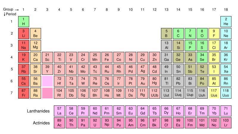
37 oping Elements! (periodic table) 37
38 oping with P (N-type)! End up with extra electrons " onor electrons! Not tightly bound to atom " Low energy to displace " Easy for these electrons to move 38
39 oping with B (P-type)! End up with electron vacancies -- Holes " Acceptor electron sites! Easy for electrons to shift into these sites " Low energy to displace " Easy for the electrons to move " Movement of an electron best viewed as movement of hole 39
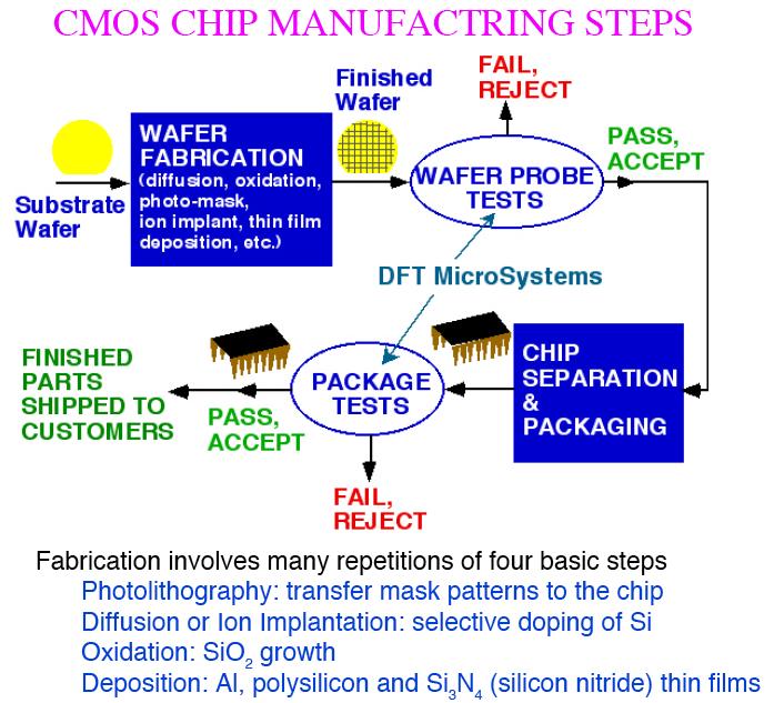
40 IC Manufacturing teps 40

41 Fabrication! tart with ilicon wafer! ope! Grow Oxide (io 2 )! eposit Metal! Mask/Etch to define where features go Time Code: 2:00-4:30 41
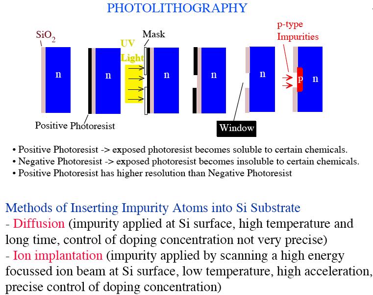
42 Photolithography 42
43 CMO Processing Technology Boron atoms deposited on surface time = 0 s time = 60 s 43

44 Fabricated n-mo Transistor 44
45 n-mo Transistor Representations Physical tructure poly field metal 1 gate oxide n + L drawn gate oxide n + p substrate (bulk) L effective Layout Representation G n+ n+ L drawn W drawn chematic Representation 45

46 nmo Transistor from a 3 Perspective Gate Oxide Field Oxide P-Type ource/rain Regions Field Oxide 46
47 Fabrication Process Grow field oxide. Create contact window, deposit & pattern metal film. 47
48 Typical N-Well CMO Process 48


49 Typical N-Well CMO Process 49
50 Big Idea! ystematic construction of any gate from transistors with CMO PUN and PN! Hierarchical design process in three domains (behavioural, structural, and physical) allows for complicated designs motivated cost as a function of performance, yield and design time 50
51 Admin! New classroom: Towne 311! Behind the scenes programming note: " Additional grader: Yifeng Zhang! Enroll in Piazza site " piazza.com/upenn/spring2019/ese570! Homework 1 due Friday " Journal articles may show up in lecture 51
Lecture Outline. ESE 570: Digital Integrated Circuits and VLSI Fundamentals. Classification of Digital CMOS Circuits. Digital CMOS Basics
 EE 570: iital Interated Circuits and VLI Fundamentals Lec 2: January 17, 2017 MO Fabrication pt. 1: Physics and Methodoloy Lecture Outline iital CMO asics VLI Fundamentals Fabrication Process 2 Classification
Lecture Outline. ESE 570: Digital Integrated Circuits and VLSI Fundamentals. Classification of Digital CMOS Circuits. Digital CMOS Basics
 EE 570: iital Interated Circuits and VLI Fundamentals Lec 2: January 19, 2016 MO Fabrication pt. 1: Physics and Methodoloy Lecture Outline! iital CMO asics! VLI Fundamentals! Fabrication Process 2 Classification
ESE 570: Digital Integrated Circuits and VLSI Fundamentals
 ESE 570: Digital Integrated Circuits and VLSI Fundamentals Lec 2: January 19, 2016 MOS Fabrication pt. 1: Physics and Methodology Lecture Outline! Digital CMOS Basics! VLSI Fundamentals! Fabrication Process
ESE 570: Digital Integrated Circuits and VLSI Fundamentals
 ESE 570: Digital Integrated Circuits and VLSI Fundamentals Lec 2: January 17, 2017 MOS Fabrication pt. 1: Physics and Methodology Lecture Outline! Digital CMOS Basics! VLSI Fundamentals! Fabrication Process
ESE370: Circuit-Level Modeling, Design, and Optimization for Digital Systems
 ESE370: Circuit-Level Modeling, Design, and Optimization for Digital Systems Lec 6: September 14, 2015 MOS Model You are Here: Transistor Edition! Previously: simple models (0 and 1 st order) " Comfortable
ESE 570: Digital Integrated Circuits and VLSI Fundamentals
 ESE 570: Digital Integrated Circuits and VLSI Fundamentals Lec 4: January 29, 2019 MOS Transistor Theory, MOS Model Penn ESE 570 Spring 2019 Khanna Lecture Outline! CMOS Process Enhancements! Semiconductor
2. BOOLEAN SWITCHING ALGEBRA
 Boolean witching Algebra 2-2. BOOLEAN WITCHIN ALEBRA Objectives. Understand Boolean algebra. 2. tudy the basic rules governing logic analysis and design. eorge Boole, 85~864 John Venn, 834~923 2. Logic
Digital Integrated Circuits A Design Perspective
 Digital Integrated Circuits Design Perspective Designing Combinational Logic Circuits Fuyuzhuo School of Microelectronics,SJTU Introduction Digital IC Dynamic Logic Introduction Digital IC 2 EE141 Dynamic
Lecture 4: Implementing Logic in CMOS
 Lecture 4: Implementing Logic in CMOS Mark Mcermott Electrical and Computer Engineering The University of Texas at ustin Review of emorgan s Theorem Recall that: () = + and = ( + ) (+) = and + = ( ) ()
ESE370: Circuit-Level Modeling, Design, and Optimization for Digital Systems. Today MOS MOS. Capacitor. Idea
 ESE370: Circuit-Level Modeling, Design, and Optimization for Digital Systems Day 9: September 26, 2011 MOS Model Today MOS Structure Basic Idea Semiconductor Physics Metals, insulators Silicon lattice
ESE370: Circuit-Level Modeling, Design, and Optimization for Digital Systems
 ESE370: Circuit-Level Modeling, Design, and Optimization for Digital Systems Lec 6: September 18, 2017 MOS Model You are Here: Transistor Edition! Previously: simple models (0 and 1 st order) " Comfortable
ESE 570: Digital Integrated Circuits and VLSI Fundamentals
 ESE 570: Digital Integrated Circuits and VLSI Fundamentals Lec 4: January 23, 2018 MOS Transistor Theory, MOS Model Penn ESE 570 Spring 2018 Khanna Lecture Outline! CMOS Process Enhancements! Semiconductor
! CMOS Process Enhancements. ! Semiconductor Physics. " Band gaps. " Field Effects. ! MOS Physics. " Cut-off. " Depletion.
 ESE 570: Digital Integrated Circuits and VLSI Fundamentals Lec 4: January 9, 019 MOS Transistor Theory, MOS Model Lecture Outline CMOS Process Enhancements Semiconductor Physics Band gaps Field Effects
Digital Integrated Circuits Designing Combinational Logic Circuits. Fuyuzhuo
 Digital Integrated Circuits Designing Combinational Logic Circuits Fuyuzhuo Introduction Digital IC Dynamic Logic Introduction Digital IC EE141 2 Dynamic logic outline Dynamic logic principle Dynamic logic
Learning Objectives 10/7/2010. CE 411 Digital System Design. Fundamental of Logic Design. Review the basic concepts of logic circuits. Dr.
 /7/ CE 4 Digital ystem Design Dr. Arshad Aziz Fundamental of ogic Design earning Objectives Review the basic concepts of logic circuits Variables and functions Boolean algebra Minterms and materms ogic
Introduction to CMOS VLSI Design Lecture 1: Introduction
 Introduction to CMOS VLSI Design Lecture 1: Introduction David Harris, Harvey Mudd College Kartik Mohanram and Steven Levitan University of Pittsburgh Introduction Integrated circuits: many transistors
VLSI Design I; A. Milenkovic 1
 PE/EE 47, PE 57 VLI esign I L6: tatic MO Logic epartment of Electrical and omputer Engineering University of labama in Huntsville leksandar Milenkovic ( www. ece.uah.edu/~milenka ) www. ece.uah.edu/~milenka/cpe57-3f
Lecture 0: Introduction
 Lecture 0: Introduction Introduction q Integrated circuits: many transistors on one chip q Very Large Scale Integration (VLSI): bucketloads! q Complementary Metal Oxide Semiconductor Fast, cheap, low power
! Previously: simple models (0 and 1 st order) " Comfortable with basic functions and circuits. ! This week and next (4 lectures)
 Comfortable with basic functions and circuits. ! This week and next (4 lectures)") ESE370: CircuitLevel Modeling, Design, and Optimization for Digital Systems Lec 6: September 14, 2015 MOS Model You are Here: Transistor Edition! Previously: simple models (0 and 1 st order) " Comfortable
ESE370: CircuitLevel Modeling, Design, and Optimization for Digital Systems Lec 6: September 14, 2015 MOS Model You are Here: Transistor Edition! Previously: simple models (0 and 1 st order) " Comfortable
Floating Point Representation and Digital Logic. Lecture 11 CS301
 Floating Point Representation and Digital Logic Lecture 11 CS301 Administrative Daily Review of today s lecture w Due tomorrow (10/4) at 8am Lab #3 due Friday (9/7) 1:29pm HW #5 assigned w Due Monday 10/8
VLSI Design I; A. Milenkovic 1
 ourse dministration PE/EE 47, PE 57 VLI esign I L6: omplementary MO Logic Gates epartment of Electrical and omputer Engineering University of labama in Huntsville leksandar Milenkovic ( www.ece.uah.edu/~milenka
EE 330 Lecture 6. Improved Switch-Level Model Propagation Delay Stick Diagrams Technology Files
 EE 330 Lecture 6 Improved witch-level Model Propagation elay tick iagrams Technology Files Review from Last Time MO Transistor Qualitative iscussion of n-channel Operation Bulk ource Gate rain rain G Gate
! CMOS Process Enhancements. ! Semiconductor Physics. " Band gaps. " Field Effects. ! MOS Physics. " Cut-off. " Depletion.
 ESE 570: Digital Integrated Circuits and VLSI Fundamentals Lec 4: January 3, 018 MOS Transistor Theory, MOS Model Lecture Outline! CMOS Process Enhancements! Semiconductor Physics " Band gaps " Field Effects!
Digital Integrated Circuits A Design Perspective
 igital Integrated Circuits esign Perspective esigning Combinational Logic Circuits 1 Combinational vs. Sequential Logic In Combinational Logic Circuit Out In Combinational Logic Circuit Out State Combinational
CPE/EE 427, CPE 527 VLSI Design I L07: CMOS Logic Gates, Pass Transistor Logic. Review: CMOS Circuit Styles
 PE/EE 427, PE 527 VLI esign I L07: MO Logic Gates, Pass Transistor Logic epartment of Electrical and omputer Engineering University of labama in Huntsville leksandar Milenkovic ( www.ece.uah.edu/~milenka
nmos IC Design Report Module: EEE 112
 nmos IC Design Report Author: 1302509 Zhao Ruimin Module: EEE 112 Lecturer: Date: Dr.Zhao Ce Zhou June/5/2015 Abstract This lab intended to train the experimental skills of the layout designing of the
VLSI Design I; A. Milenkovic 1
 ourse dministration PE/EE 47, PE 57 VLI esign I L6: tatic MO Logic epartment of Electrical and omputer Engineering University of labama in Huntsville leksandar Milenkovic ( www. ece.uah.edu/~milenka )
CMPEN 411 VLSI Digital Circuits. Lecture 04: CMOS Inverter (static view)
") CMPEN 411 VLSI Digital Circuits Lecture 04: CMOS Inverter (static view) Kyusun Choi [Adapted from Rabaey s Digital Integrated Circuits, Second Edition, 2003 J. Rabaey, A. Chandrakasan, B. Nikolic] CMPEN
CMPEN 411 VLSI Digital Circuits Lecture 04: CMOS Inverter (static view) Kyusun Choi [Adapted from Rabaey s Digital Integrated Circuits, Second Edition, 2003 J. Rabaey, A. Chandrakasan, B. Nikolic] CMPEN
Chapter 2. Design and Fabrication of VLSI Devices
 Chapter 2 Design and Fabrication of VLSI Devices Jason Cong 1 Design and Fabrication of VLSI Devices Objectives: To study the materials used in fabrication of VLSI devices. To study the structure of devices
CPE/EE 427, CPE 527 VLSI Design I L06: CMOS Inverter, CMOS Logic Gates. Course Administration. CMOS Inverter: A First Look
 CPE/EE 47, CPE 57 VLSI esign I L6: CMOS Inverter, CMOS Logic Gates epartment of Electrical and Computer Engineering University of labama in Huntsville leksandar Milenkovic ( www.ece.uah.edu/~milenka )
CMOS Inverter (static view)
") Review: Design Abstraction Levels SYSTEM CMOS Inverter (static view) + MODULE GATE [Adapted from Chapter 5. 5.3 CIRCUIT of G DEVICE Rabaey s Digital Integrated Circuits,, J. Rabaey et al.] S D Review:
Review: Design Abstraction Levels SYSTEM CMOS Inverter (static view) + MODULE GATE [Adapted from Chapter 5. 5.3 CIRCUIT of G DEVICE Rabaey s Digital Integrated Circuits,, J. Rabaey et al.] S D Review:
Lecture Outline. ESE 570: Digital Integrated Circuits and VLSI Fundamentals. Review: 1st Order RC Delay Models. Review: Two-Input NOR Gate (NOR2)
") ESE 570: Digital Integrated Circuits and VLSI Fundamentals Lec 14: March 1, 2016 Combination Logic: Ratioed and Pass Logic Lecture Outline! CMOS Gates Review " CMOS Worst Case Analysis! Ratioed Logic Gates!
ESE 570: Digital Integrated Circuits and VLSI Fundamentals Lec 14: March 1, 2016 Combination Logic: Ratioed and Pass Logic Lecture Outline! CMOS Gates Review " CMOS Worst Case Analysis! Ratioed Logic Gates!
Topics. Dynamic CMOS Sequential Design Memory and Control. John A. Chandy Dept. of Electrical and Computer Engineering University of Connecticut
 Topics Dynamic CMOS Sequential Design Memory and Control Dynamic CMOS In static circuits at every point in time (except when switching) the output is connected to either GND or V DD via a low resistance
Dynamic Combinational Circuits. Dynamic Logic
 Dynamic Combinational Circuits Dynamic circuits Charge sharing, charge redistribution Domino logic np-cmos (zipper CMOS) Krish Chakrabarty 1 Dynamic Logic Dynamic gates use a clocked pmos pullup Two modes:
EE141Microelettronica. CMOS Logic
 Microelettronica CMOS Logic CMOS logic Power consumption in CMOS logic gates Where Does Power Go in CMOS? Dynamic Power Consumption Charging and Discharging Capacitors Short Circuit Currents Short Circuit
! Previously: simple models (0 and 1 st order) " Comfortable with basic functions and circuits. ! This week and next (4 lectures)
 Comfortable with basic functions and circuits. ! This week and next (4 lectures)") ESE370: CircuitLevel Modeling, Design, and Optimization for Digital Systems Lec 6: September 18, 2017 MOS Model You are Here: Transistor Edition! Previously: simple models (0 and 1 st order) " Comfortable
ESE370: CircuitLevel Modeling, Design, and Optimization for Digital Systems Lec 6: September 18, 2017 MOS Model You are Here: Transistor Edition! Previously: simple models (0 and 1 st order) " Comfortable
EE40 Lec 20. MOS Circuits
 EE40 Lec 20 MOS Circuits eading: Chap. 12 of Hambley Supplement reading on MOS Circuits http://www.inst.eecs.berkeley.edu/~ee40/fa09/handouts/ee40_mos_circuit.pdf Slide 1 Bias circuits OUTLINE Smallsignal
AE74 VLSI DESIGN JUN 2015
 Q.2 a. Write down the different levels of integration of IC industry. (4) b. With neat sketch explain briefly PMOS & NMOS enhancement mode transistor. N-MOS enhancement mode transistor:- This transistor
KINGS COLLEGE OF ENGINEERING DEPARTMENT OF ELECTRONICS AND COMMUNICATION ENGINEERING QUESTION BANK
 KINGS COLLEGE OF ENGINEERING DEPARTMENT OF ELECTRONICS AND COMMUNICATION ENGINEERING QUESTION BANK SUBJECT CODE: EC 1354 SUB.NAME : VLSI DESIGN YEAR / SEMESTER: III / VI UNIT I MOS TRANSISTOR THEORY AND
Lecture 5 Fault Modeling
 Lecture 5 Fault Modeling Why model faults? Some real defects in VLSI and PCB Common fault models Stuck-at faults Single stuck-at faults Fault equivalence Fault dominance and checkpoint theorem Classes
Fig. 1 CMOS Transistor Circuits (a) Inverter Out = NOT In, (b) NOR-gate C = NOT (A or B)
 Inverter Out = NOT In, (b) NOR-gate C = NOT (A or B)") 1 Introduction to Transistor-Level Logic Circuits 1 By Prawat Nagvajara At the transistor level of logic circuits, transistors operate as switches with the logic variables controlling the open or closed
1 Introduction to Transistor-Level Logic Circuits 1 By Prawat Nagvajara At the transistor level of logic circuits, transistors operate as switches with the logic variables controlling the open or closed
Today s lecture. EE141- Spring 2003 Lecture 4. Design Rules CMOS Inverter MOS Transistor Model
 - Spring 003 Lecture 4 Design Rules CMOS Inverter MOS Transistor Model Today s lecture Design Rules The CMOS inverter at a glance An MOS transistor model for manual analysis Important! Labs start next
ESE 570: Digital Integrated Circuits and VLSI Fundamentals
 ESE 570: Digital Integrated Circuits and VLSI Fundamentals Lec 4: January 24, 2017 MOS Transistor Theory, MOS Model Penn ESE 570 Spring 2017 Khanna Lecture Outline! Semiconductor Physics " Band gaps "
3. Design a stick diagram for the PMOS logic shown below [16] Y = (A + B).C. 4. Design a layout diagram for the CMOS logic shown below [16]
![3. Design a stick diagram for the PMOS logic shown below [16] Y = (A + B).C. 4. Design a layout diagram for the CMOS logic shown below [16]](/thumbs/96/128765118.jpg "3. Design a stick diagram for the PMOS logic shown below [16] Y = (A + B).C. 4. Design a layout diagram for the CMOS logic shown below [16]") Code No: RR420203 Set No. 1 1. (a) Find g m and r ds for an n-channel transistor with V GS = 1.2V; V tn = 0.8V; W/L = 10; µncox = 92 µa/v 2 and V DS = Veff + 0.5V The out put impedance constant. λ = 95.3
Code No: RR420203 Set No. 1 1. (a) Find g m and r ds for an n-channel transistor with V GS = 1.2V; V tn = 0.8V; W/L = 10; µncox = 92 µa/v 2 and V DS = Veff + 0.5V The out put impedance constant. λ = 95.3
Dynamic Combinational Circuits. Dynamic Logic
 Dynamic Combinational Circuits Dynamic circuits Charge sharing, charge redistribution Domino logic np-cmos (zipper CMOS) Krish Chakrabarty 1 Dynamic Logic Dynamic gates use a clocked pmos pullup Two modes:
Lecture 1: Circuits & Layout
 Lecture 1: Circuits & Layout Outline q A Brief History q CMOS Gate esign q Pass Transistors q CMOS Latches & Flip-Flops q Standard Cell Layouts q Stick iagrams 2 A Brief History q 1958: First integrated
EEC 118 Lecture #6: CMOS Logic. Rajeevan Amirtharajah University of California, Davis Jeff Parkhurst Intel Corporation
 EEC 118 Lecture #6: CMOS Logic Rajeevan mirtharajah University of California, Davis Jeff Parkhurst Intel Corporation nnouncements Quiz 1 today! Lab 2 reports due this week Lab 3 this week HW 3 due this
The Intrinsic Silicon
 The Intrinsic ilicon Thermally generated electrons and holes Carrier concentration p i =n i ni=1.45x10 10 cm-3 @ room temp Generally: n i = 3.1X10 16 T 3/2 e -1.21/2KT cm -3 T= temperature in K o (egrees
CMOS Inverter: CPE/EE 427, CPE 527 VLSI Design I L06: CMOS Inverter, CMOS Logic Gates. Course Administration. CMOS Properties.
 CMOS Inverter: Steady State Response CPE/EE 47, CPE 57 VLSI esign I L6: CMOS Inverter, CMOS Logic Gates R p V OL = V OH = V M = f(r n, R p ) epartment of Electrical and Computer Engineering University
ESE 570: Digital Integrated Circuits and VLSI Fundamentals
 ESE 570: Digital Integrated Circuits and VLSI Fundamentals Lec 18: March 27, 2018 Dynamic Logic, Charge Injection Lecture Outline! Sequential MOS Logic " D-Latch " Timing Constraints! Dynamic Logic " Domino
ENGR890 Digital VLSI Design Fall Lecture 4: CMOS Inverter (static view)
") ENGR89 Digital VLSI Design Fall 5 Lecture 4: CMOS Inverter (static view) [Adapted from Chapter 5 of Digital Integrated Circuits, 3, J. Rabaey et al.] [Also borrowed from Vijay Narayanan and Mary Jane Irwin]
ENGR89 Digital VLSI Design Fall 5 Lecture 4: CMOS Inverter (static view) [Adapted from Chapter 5 of Digital Integrated Circuits, 3, J. Rabaey et al.] [Also borrowed from Vijay Narayanan and Mary Jane Irwin]
Topics. CMOS Design Multi-input delay analysis. John A. Chandy Dept. of Electrical and Computer Engineering University of Connecticut
 Topics CMO Design Multi-input delay analysis pring 25 Transmission Gate OUT Z OUT Z pring 25 Transmission Gate OUT When is low, the output is at high impedance When is high, the output follows However,
L2: Combinational Logic Design (Construction and Boolean Algebra)
") L2: Combinational Logic Design (Construction and Boolean Algebra) Acknowledgements: Lecture material adapted from Chapter 2 of R. Katz, G. Borriello, Contemporary Logic Design (second edition), Pearson
L2: Combinational Logic Design (Construction and Boolean Algebra) Acknowledgements: Lecture material adapted from Chapter 2 of R. Katz, G. Borriello, Contemporary Logic Design (second edition), Pearson
Lecture Outline. ESE 570: Digital Integrated Circuits and VLSI Fundamentals. Review: MOSFET N-Type, P-Type. Semiconductor Physics.
 ESE 57: Digital Integrated Circuits and VLSI Fundamentals Lec 4: January 24, 217 MOS Transistor Theory, MOS Model Lecture Outline! Semiconductor Physics " Band gaps " Field Effects! MOS Physics " Cutoff
VLSI VLSI CIRCUIT DESIGN PROCESSES P.VIDYA SAGAR ( ASSOCIATE PROFESSOR) Department of Electronics and Communication Engineering, VBIT
 Department of Electronics and Communication Engineering, VBIT") VLSI VLSI CIRCUIT DESIGN PROCESSES P.VIDYA SAGAR ( ASSOCIATE PROFESSOR) SYLLABUS UNIT II VLSI CIRCUIT DESIGN PROCESSES: VLSI Design Flow, MOS Layers, Stick Diagrams, Design Rules and Layout, 2 m CMOS Design
VLSI VLSI CIRCUIT DESIGN PROCESSES P.VIDYA SAGAR ( ASSOCIATE PROFESSOR) SYLLABUS UNIT II VLSI CIRCUIT DESIGN PROCESSES: VLSI Design Flow, MOS Layers, Stick Diagrams, Design Rules and Layout, 2 m CMOS Design
EE 5211 Analog Integrated Circuit Design. Hua Tang Fall 2012
 EE 5211 Analog Integrated Circuit Design Hua Tang Fall 2012 Today s topic: 1. Introduction to Analog IC 2. IC Manufacturing (Chapter 2) Introduction What is Integrated Circuit (IC) vs discrete circuits?
Digital Integrated Circuits A Design Perspective. Semiconductor. Memories. Memories
 Digital Integrated Circuits A Design Perspective Semiconductor Chapter Overview Memory Classification Memory Architectures The Memory Core Periphery Reliability Case Studies Semiconductor Memory Classification
ECE 546 Lecture 10 MOS Transistors
 ECE 546 Lecture 10 MOS Transistors Spring 2018 Jose E. Schutt-Aine Electrical & Computer Engineering University of Illinois jesa@illinois.edu NMOS Transistor NMOS Transistor N-Channel MOSFET Built on p-type
UNIVERSITY OF CALIFORNIA College of Engineering Department of Electrical Engineering and Computer Sciences. Professor Oldham Fall 1999
 UNIVERSITY OF CLIFORNI College of Engineering Department of Electrical Engineering and Computer Sciences Professor Oldham Fall 1999 EECS 40 FINL EXM 13 December 1999 Name: Last, First Student ID: T: Kusuma
EEC 116 Lecture #5: CMOS Logic. Rajeevan Amirtharajah Bevan Baas University of California, Davis Jeff Parkhurst Intel Corporation
 EEC 116 Lecture #5: CMOS Logic Rajeevan mirtharajah Bevan Baas University of California, Davis Jeff Parkhurst Intel Corporation nnouncements Quiz 1 today! Lab 2 reports due this week Lab 3 this week HW
Field-Effect (FET) transistors
 transistors") Field-Effect (FET) transistors References: Barbow (Chapter 8), Rizzoni (chapters 8 & 9) In a field-effect transistor (FET), the width of a conducting channel in a semiconductor and, therefore, its current-carrying
Field-Effect (FET) transistors References: Barbow (Chapter 8), Rizzoni (chapters 8 & 9) In a field-effect transistor (FET), the width of a conducting channel in a semiconductor and, therefore, its current-carrying
MOS Transistor Properties Review
 MOS Transistor Properties Review 1 VLSI Chip Manufacturing Process Photolithography: transfer of mask patterns to the chip Diffusion or ion implantation: selective doping of Si substrate Oxidation: SiO
ENEE 359a Digital VLSI Design
 SLIDE 1 ENEE 359a Digital VLSI Design Prof. blj@eng.umd.edu Credit where credit is due: Slides contain original artwork ( Jacob 2004) as well as material taken liberally from Irwin & Vijay s CSE477 slides
Semiconductor Memories
 Semiconductor References: Adapted from: Digital Integrated Circuits: A Design Perspective, J. Rabaey UCB Principles of CMOS VLSI Design: A Systems Perspective, 2nd Ed., N. H. E. Weste and K. Eshraghian
CARNEGIE MELLON UNIVERSITY DEPARTMENT OF ELECTRICAL AND COMPUTER ENGINEERING DIGITAL INTEGRATED CIRCUITS FALL 2002
 CARNEGIE MELLON UNIVERSITY DEPARTMENT OF ELECTRICAL AND COMPUTER ENGINEERING 18-322 DIGITAL INTEGRATED CIRCUITS FALL 2002 Final Examination, Monday Dec. 16, 2002 NAME: SECTION: Time: 180 minutes Closed
9/18/2008 GMU, ECE 680 Physical VLSI Design
 ECE680: Physical VLSI Design Chapter III CMOS Device, Inverter, Combinational circuit Logic and Layout Part 3 Combinational Logic Gates (textbook chapter 6) 9/18/2008 GMU, ECE 680 Physical VLSI Design
CMOS Transistors, Gates, and Wires
 CMOS Transistors, Gates, and Wires Should the hardware abstraction layers make today s lecture irrelevant? pplication R P C W / R W C W / 6.375 Complex Digital Systems Christopher atten February 5, 006
CMOS Technology Worksheet
 CMOS Technology Worksheet Concept Inventory: Notes: PFET, NFET: voltage controlled switches CMOS composition rules: complementary pullup and pulldown CMOS gates are naturally inverting t PD and t CD timing
Static CMOS Circuits. Example 1
 Static CMOS Circuits Conventional (ratio-less) static CMOS Covered so far Ratio-ed logic (depletion load, pseudo nmos) Pass transistor logic ECE 261 Krish Chakrabarty 1 Example 1 module mux(input s, d0,
Important! EE141- Fall 2002 Lecture 5. CMOS Inverter MOS Transistor Model
 - Fall 00 Lecture 5 CMO Inverter MO Transistor Model Important! Lab 3 this week You must show up in one of the lab sessions this week If you don t show up you will be dropped from the class» Unless you
Lecture Outline. ESE 570: Digital Integrated Circuits and VLSI Fundamentals. Total Power. Energy and Power Optimization. Worksheet Problem 1
 ESE 570: Digital Integrated Circuits and VLSI Fundamentals Lec 16: March 20, 2018 Energy and Power Optimization, Design Space Exploration Lecture Outline! Energy and Power Optimization " Tradeoffs! Design
ESE 570: Digital Integrated Circuits and VLSI Fundamentals
 ESE 570: Digital Integrated Circuits and VLSI Fundamentals Lec 17: March 23, 2017 Energy and Power Optimization, Design Space Exploration, Synchronous MOS Logic Lecture Outline! Energy and Power Optimization
S No. Questions Bloom s Taxonomy Level UNIT-I
 GROUP-A (SHORT ANSWER QUESTIONS) S No. Questions Bloom s UNIT-I 1 Define oxidation & Classify different types of oxidation Remember 1 2 Explain about Ion implantation Understand 1 3 Describe lithography
B.Supmonchai June 26, q Introduction of device basic equations. q Introduction of models for manual analysis.
 June 26, 2004 oal of this chapter Chapter 2 MO Transistor Theory oonchuay upmonchai Integrated esign Application Research (IAR) Laboratory June 16th, 2004; Revised June 16th, 2005 q Present intuitive understanding
ESE 570: Digital Integrated Circuits and VLSI Fundamentals
 ESE 570: Digital Integrated Circuits and VLSI Fundamentals Lec 19: March 29, 2018 Memory Overview, Memory Core Cells Today! Charge Leakage/Charge Sharing " Domino Logic Design Considerations! Logic Comparisons!
ECE321 Electronics I
 ECE321 Electronics I Lecture 1: Introduction to Digital Electronics Payman Zarkesh-Ha Office: ECE Bldg. 230B Office hours: Tuesday 2:00-3:00PM or by appointment E-mail: payman@ece.unm.edu Slide: 1 Textbook
CMPE12 - Notes chapter 1. Digital Logic. (Textbook Chapter 3)
") CMPE12 - Notes chapter 1 Digital Logic (Textbook Chapter 3) Transistor: Building Block of Computers Microprocessors contain TONS of transistors Intel Montecito (2005): 1.72 billion Intel Pentium 4 (2000):
CMPE12 - Notes chapter 1 Digital Logic (Textbook Chapter 3) Transistor: Building Block of Computers Microprocessors contain TONS of transistors Intel Montecito (2005): 1.72 billion Intel Pentium 4 (2000):
CMOS Digital Integrated Circuits Lec 10 Combinational CMOS Logic Circuits
 Lec 10 Combinational CMOS Logic Circuits 1 Combinational vs. Sequential Logic In Combinational Logic circuit Out In Combinational Logic circuit Out State Combinational The output is determined only by
Integrated Circuits & Systems
 Federal University of Santa Catarina Center for Technology Computer Science & Electronics Engineering Integrated Circuits & Systems INE 5442 Lecture 18 CMOS Sequential Circuits - 1 guntzel@inf.ufsc.br
Digital Integrated Circuits A Design Perspective
 Semiconductor Memories Adapted from Chapter 12 of Digital Integrated Circuits A Design Perspective Jan M. Rabaey et al. Copyright 2003 Prentice Hall/Pearson Outline Memory Classification Memory Architectures
Lecture 7 Circuit Delay, Area and Power
 Lecture 7 Circuit Delay, Area and Power lecture notes from S. Mitra Intro VLSI System course (EE271) Introduction to VLSI Systems 1 Circuits and Delay Introduction to VLSI Systems 2 Power, Delay and Area:
ELEN0037 Microelectronic IC Design. Prof. Dr. Michael Kraft
 ELEN0037 Microelectronic IC Design Prof. Dr. Michael Kraft Lecture 2: Technological Aspects Technology Passive components Active components CMOS Process Basic Layout Scaling CMOS Technology Integrated
CPE/EE 427, CPE 527 VLSI Design I Delay Estimation. Department of Electrical and Computer Engineering University of Alabama in Huntsville
 CPE/EE 47, CPE 57 VLSI Design I Delay Estimation Department of Electrical and Computer Engineering University of labama in Huntsville leksandar Milenkovic ( www.ece.uah.edu/~milenka ) Review: CMOS Circuit
FIELD EFFECT TRANSISTORS:
 Chapter 10 FIEL EFFECT TRANITOR: MOFET The following overview gures describe important issues related to the most important electronic device. NUMBER OF ACTIVE EVICE/CHIP MOORE' LAW Gordon Moore, co-founder
CMOS INVERTER. Last Lecture. Metrics for qualifying digital circuits. »Cost» Reliability» Speed (delay)»performance
»performance") CMOS INVERTER Last Lecture Metrics for qualifying digital circuits»cost» Reliability» Speed (delay)»performance 1 Today s lecture The CMOS inverter at a glance An MOS transistor model for manual analysis
CMOS INVERTER Last Lecture Metrics for qualifying digital circuits»cost» Reliability» Speed (delay)»performance 1 Today s lecture The CMOS inverter at a glance An MOS transistor model for manual analysis
! Charge Leakage/Charge Sharing. " Domino Logic Design Considerations. ! Logic Comparisons. ! Memory. " Classification. " ROM Memories.
 ESE 57: Digital Integrated Circuits and VLSI Fundamentals Lec 9: March 9, 8 Memory Overview, Memory Core Cells Today! Charge Leakage/ " Domino Logic Design Considerations! Logic Comparisons! Memory " Classification
MOSFET: Introduction
 E&CE 437 Integrated VLSI Systems MOS Transistor 1 of 30 MOSFET: Introduction Metal oxide semiconductor field effect transistor (MOSFET) or MOS is widely used for implementing digital designs Its major
Lecture 14: Circuit Families
 Introduction to CMOS VLSI Design Lecture 4: Circuit Families David Harris, Harvey Mudd College Kartik Mohanram and Steven Levitan University of Pittsburgh Outline q Pseudo-nMOS Logic q Dynamic Logic q
CPE/EE 427, CPE 527 VLSI Design I Pass Transistor Logic. Review: CMOS Circuit Styles
 PE/EE 427, PE 527 VLI Design I Pass Transistor Logic Department of Electrical and omputer Engineering University of labama in Huntsville leksandar Milenkovic ( www.ece.uah.edu/~milenka ) Review: MO ircuit
Introduction to Computer Engineering ECE 203
 Introduction to Computer Engineering ECE 203 Northwestern University Department of Electrical Engineering and Computer Science Teacher: Robert Dick Office: L477 Tech Email: dickrp@ece.northwestern.edu
CMPEN 411 VLSI Digital Circuits Spring 2011 Lecture 07: Pass Transistor Logic
 CMPEN 411 VLSI Digital Circuits Spring 2011 Lecture 07: Pass Transistor Logic [dapted from Rabaey s Digital Integrated Circuits, Second Edition, 2003 J. Rabaey,. Chandrakasan,. Nikolic] Sp11 CMPEN 411
Lecture 150 Basic IC Processes (10/10/01) Page ECE Analog Integrated Circuits and Systems P.E. Allen
 Page ECE Analog Integrated Circuits and Systems P.E. Allen") Lecture 150 Basic IC Processes (10/10/01) Page 1501 LECTURE 150 BASIC IC PROCESSES (READING: TextSec. 2.2) INTRODUCTION Objective The objective of this presentation is: 1.) Introduce the fabrication of
Lecture 150 Basic IC Processes (10/10/01) Page 1501 LECTURE 150 BASIC IC PROCESSES (READING: TextSec. 2.2) INTRODUCTION Objective The objective of this presentation is: 1.) Introduce the fabrication of
Motivation for Lecture. For digital design we use CMOS transistors. Gate Source. CMOS symboler. MOS transistor. Depletion. A channel is created
 Motivation for Lecture igital Integrated ircuits iktor Öwall o see how standard gates are implemented with transistors? How does technology affect the performance, e.g. speed and power consumption? What
THE INVERTER. Inverter
 THE INVERTER DIGITAL GATES Fundamental Parameters Functionality Reliability, Robustness Area Performance» Speed (delay)» Power Consumption» Energy Noise in Digital Integrated Circuits v(t) V DD i(t) (a)
Chapter 5 CMOS Logic Gate Design
 Chapter 5 CMOS Logic Gate Design Section 5. -To achieve correct operation of integrated logic gates, we need to satisfy 1. Functional specification. Temporal (timing) constraint. (1) In CMOS, incorrect
EECS 312: Digital Integrated Circuits Midterm Exam 2 December 2010
 Signature: EECS 312: Digital Integrated Circuits Midterm Exam 2 December 2010 obert Dick Show your work. Derivations are required for credit; end results are insufficient. Closed book. No electronic mental
Lecture 22 Chapters 3 Logic Circuits Part 1
 Lecture 22 Chapters 3 Logic Circuits Part 1 LC-3 Data Path Revisited How are the components Seen here implemented? 5-2 Computing Layers Problems Algorithms Language Instruction Set Architecture Microarchitecture
Lecture 6 Power Zhuo Feng. Z. Feng MTU EE4800 CMOS Digital IC Design & Analysis 2010
 EE4800 CMOS Digital IC Design & Analysis Lecture 6 Power Zhuo Feng 6.1 Outline Power and Energy Dynamic Power Static Power 6.2 Power and Energy Power is drawn from a voltage source attached to the V DD
ESE 570: Digital Integrated Circuits and VLSI Fundamentals
 ESE 570: Digital Integrated Circuits and VLSI Fundamentals Lec 15: March 15, 2018 Euler Paths, Energy Basics and Optimization Midterm! Midterm " Mean: 89.7 " Standard Dev: 8.12 2 Lecture Outline! Euler
Digital Integrated Circuits A Design Perspective
 Digital Integrated Circuits Design Perspective Jan M. Rabaey nantha Chandrakasan orivoje Nikolić Designing Combinational Logic Circuits November 2002. 1 Combinational vs. Sequential Logic In Combinational