Analog and Telecommunication Electronics
|
|
|
- Dominic Dawson
- 5 years ago
- Views:
Transcription
1 Politecnico di Torino - ICT School Analog and Telecommunication Electronics D3 - A/D converters» Error taxonomy» ADC parameters» Structures and taxonomy» Mixed converters» Origin of errors 12/05/ ATLCE - D DDC
2 Lesson D3: ADC taxonomy and errors Analog to Digital converters Transfer function and error taxonomy (linear, nonlinear, dynamic) Converter parameters: complexity and speed Examples of A/D converters Flash, Tracking, Successive approximation Residue, subranging, folding structures Pipeline structures Mixed structures Performance tradeoff Text reference Sect /05/ ATLCE - D DDC
3 Errors in A/D converters Dual transfer function vs D/A X axis: analog values (continuous) Y axis: numeric values (discrete) Each A Di interval corresponds to a D i value stair transfer function If N large looks as a continuous line Same error classification as D/A» Linear: offset and gain» Nonlinearity: differential and integral» Dynamic parameters 12/05/ ATLCE - D DDC
4 Ideal A/D transfer function D (digital) M Di LSB A (analog) A Di A D 0 S 12/05/ ATLCE - D DDC
5 Static errors: two-steps analysis Linear approximation of actual transfer function Actual transfer function vs linear approximation Nonlinearity errors: integral nonlinearity Linear approximation vs ideal transfer function Linear errors: offset and gain Detailed quantization interval analysis Differential nonlinearity 12/05/ ATLCE - D DDC
6 Actual vs ideal transfer function M D ideal 0 0 Actual transfer function S A 12/05/ ATLCE - D DDC
7 Best linear approximation M D Best approx. straigth line 0 0 Actual transfer function S A 12/05/ ATLCE - D DDC
8 Linear approx. vs ideal transf. function M D ideal G Best approx. straigth line O 0 0 S A 12/05/ ATLCE - D DDC
9 Integral nonlinearity error M D integral nonlinearity Nonlinearity band error inl Best approx. straigth line 0 0 Actual transfer function S A 12/05/ ATLCE - D DDC
10 Complete view M D integral nonlinearity Nonlinearity band ideal error inl Best approx. straigth line 0 0 Actual transfer function S A 12/05/ ATLCE - D DDC
11 Linear and nonlinear errors Offset error shift of the output Gain errors rotation of the transfer function Both can be compensated with gain and offset corrections in the signal chain Integral nonlinearity error inl Position dependent; cannot be compensated 12/05/ ATLCE - D DDC
12 Ideal A/D transfer function Uniform quantization: All quantization intervals AD have the same amplitude M D A D 0 0 S A 12/05/ ATLCE - D DDC
13 Integral nonlinearity error Actual quantization intervals: A D A D Differential nonlinearity: DNL = A D -A D M D Ideal transfer function A D 0 A D 0 S Actual transfer function A 12/05/ ATLCE - D DDC
14 Missing code error Wide intervals reduce adjacent ones Very wide intervals can suppress adjacent ones Missing code error: DNL > 1 LSB M D A D1 A D2 0 0 S This code is never generated A 12/05/ ATLCE - D DDC
15 Integral and differential nonlinearity Integral nonlinearity INL How much the global transfer function deviates from a straight line Unique figure Differential nonlinearity DNL Difference A D -A D between ideal (A D ) and actual (A D ) amplitude of each quantization interval Specific to each interval (but has a max!) INL = ( DNL ) = ( DNL ) DNL = Der( INL ) 12/05/ ATLCE - D DDC
16 Relation Integral/differential nonlinearity ε INL = ( DNL ) = ( DNL ) ε DNL = Der( INL ) Example Fixed polarity ε DNL high ε INL Alternate polarity ε DNL low ε INL 12/05/ ATLCE - D DDC
17 Dynamic parameters Conversion from A to D requires some time: conversion time Tc Can be specified also as conversion frequency Fc = 1/Tc In most cases The ADC receives a Conversion Start (CS) command After Tc the ADC raises a End Of Conversion (EOC) flag. Some ADC can follow a (slowly) changing signal: tracking converters Dynamic behavior specified by max track rate (Slew Rate) 12/05/ ATLCE - D DDC
18 ADC error summary Linear errors: Gain: G offset: O Nonlinearity errors: Integral NL: inl differential NL: dnl Dynamic parameters Conversion time: t C Tracking rate: dv/dt 12/05/ ATLCE - D DDC
19 Lesson D3: A/D converters Analog to Digital converters Error taxonomy (linear, nonlinear, dynamic) Converter parameters: complexity and speed Examples of A/D converters Flash, Tracking Successive approximation, Residue/subranging Pipeline structures Performance tradeoff 12/05/ ATLCE - D DDC
20 A/D converter architectures Various types of ADC, which can be classified from: Complexity» Number of comparators in the circuit» Better if few comparators Conversion time Tc» Or conversion rate Fc, inverse of Tc» Better if low Tc (high speed, high Fc) Linked parameters: High speed converters are more complex High speed and high resolution are expensive. 12/05/ ATLCE - D DDC
21 A/D converters classification Complexity Conv time Parallel (flash) Pipeline Residue Successive approximation Tracking, Ramp Complexity: number of comparators. Conversion time: Tc = 1/Fc (inverse of the number of conversion/s). 12/05/ ATLCE - D DDC
22 Parallel (flash) ADC V R thermometric or linear output coding A Analog input level (between 0 and V R ) 12/05/ ATLCE - D DDC
23 Flash ADC with coded output V R M N encoder A M-N enc M = 2 N -1 N 12/05/ ATLCE - D DDC
24 Flash converter parameters 2 N comparators (2 N -1) 1 comparison cycle for N bits Fast all comparators operate in the same time slot Complex requires many comparators 12/05/ ATLCE - D DDC
25 DAC - feedback converters A logic network builds an approximation A of the input A using results of A<--> A comparison A is obtained from D through a DAC D is the numeric representation of A A A + - Logic network DAC D 12/05/ ATLCE - D DDC
26 Feedback converters algorithms The logic network modifies D till A becomes the best approximation of A (within the N-bit resolution) Two procedures: Steps of one LSB: tracking converters 2 N steps for full scale change; conversion time: T C = 2 N T CK Start from MSB: successive approximation converters N steps for any conversion: T C = N T CK 12/05/ ATLCE - D DDC
27 LSB steps: staircase converter Counter with enable If A < A, EN = 1 (counter enabled) If A > A, EN = 0 (counter disabled) M = 2 N steps from 0 to S:T C = 2 N T CK A A + - EN counter CK DAC D 12/05/ ATLCE - D DDC
28 Signal acquisition with staircase ADC As long as A < A, EN = 1 and counter is enabled, The feedback signal A goes up 1 LSB for each Tck As A > A the comparator disables the counter; A stops max conversion time: Tc max (0 to S change of A) = 2 N Tck For new conversion reset counter to 0 12/05/ ATLCE - D DDC
29 LSB steps: tracking converter Up/Down counter If A < A, D = D + 1 If A > A, D = D - 1 M = 2 N steps from 0 to S:T C = 2 N T CK A A + - U/D U/D counter CK DAC D 12/05/ ATLCE - D DDC
30 Acquisition of constant signal As long as A < A, counter goes UP on CK edges The feedback signal A moves 1 LSB for each Tck As A > A the counter reverses count direction max conversion time: Tc max (0 to S change of A) = 2 N Tck 12/05/ ATLCE - D DDC
31 Tracking of changing signals The converter can track signals with dv/dt < A D /Tck Overload Tracking 12/05/ ATLCE - D DDC
32 Tracking converter parameters 1 comparator 2 N comparison cycle for N bits Slow fully sequential decisions limited dv/dt tracking capability Simple requires a single comparator 12/05/ ATLCE - D DDC
33 Start with MSB: succ. approx. ADC Input signal compared with S/2: result --> MSB MSB = 0: next comparison with S/4 MSB = 1: next comparison with 3S/4 result --> MSB A A + - Successive approximation register (SAR) DAC D 12/05/ ATLCE - D DDC
34 Approximation sequence - 1 Input signal A S A S/2 0 t 12/05/ ATLCE - D DDC
35 Approximation sequence - 2 A is compared with S/2 A = S/2 by setting MSB = 1 S A S/2 0 t A = S/2 12/05/ ATLCE - D DDC
36 Approximation sequence - 3 Since A > S/2, MSB = S/2 excluded from possible A values S A S/2 0 t A = S/2 A > A MSB = 1 12/05/ ATLCE - D DDC
37 Approximation sequence - 4 A compared with mid-value of possible range A = 3S/4 by setting MSB-1 = 1 S A 3S/4 S/2 0 t A = S/2 A > A MSB = 1 A = 3S/4 12/05/ ATLCE - D DDC
38 Approximation sequence - 5 Since A < 3S/4, MSB -1 = 0 3S/4 - S range excluded from possible A values S A 3S/4 S/2 0 t A = S/2 A > A MSB = 1 A = 3S/4 A < A MSB-1 = 0 12/05/ ATLCE - D DDC
39 Approximation sequence - 6 A is compared with mid-value of possible range A = 5S/8 by setting MSB - 2 = 1 S A 3S/4 S/2 0 t A = S/2 A > A MSB = 1 A = 3S/4 A < A MSB-1 = 0 A = 5S/8 12/05/ ATLCE - D DDC
40 Approximation sequence - 7 Since A < 5S/8, MSB - 2 = 1 S/2-5S/8 range excluded from possible A values S A 3S/4 S/2 0 t A = S/2 A > A MSB = 1 A = 3S/4 A < A MSB-1 = 0 A = 5S/8 A > A MSB-2 = 1 A = 11S/16 12/05/ ATLCE - D DDC
41 Approximation sequence - 8 Since A < 11S/16, MSB - 3 must be 0 11S/16-3S/4 range excluded from possible A values S A 3S/4 S/2 0 t A = S/2 A > A MSB = 1 A = 3S/4 A < A MSB-1 = 0 A = 5S/8 A > A MSB-2 = 1 A = 11S/16 A < A MSB-3 = 0 12/05/ ATLCE - D DDC
42 Complete decision tree S 3S/4 S/2 0 t Sequence of possible output A from D/A which are compared with A 12/05/ ATLCE - D DDC
43 Successive approx. ADC parameters Single comparator N comparison cycles for N-bit conversion Vs flash ADC Simpler: 1 comparator vs 2 N Slower: N steps vs 1 Vs tracking ADC Same complexity: 1 comparator faster: N steps vs 2 N 12/05/ ATLCE - D DDC
44 Speed vs complexity Complex Conv time Parallel (flash) 2 N 1??? (Pipeline) N 1??? (Residue) N N Successive Approx 1 N Tracking 1 2 N Complexity: Conversion time: proportional to the number of comparators. the maximum number of comparator delay (clock periods) to complete a conversion the table suggest two new types of ADC. 12/05/ ATLCE - D DDC
45 Lesson D3: A/D converters Analog to Digital converters Error taxonomy (linear, nonlinear, dynamic) Converter parameters: complexity and speed Examples of A/D converters Flash, Tracking Successive approximation, Residue/subranging Pipeline structures Performance tradeoff 12/05/ ATLCE - D DDC
46 Comparison in SAR ADC Sequence of comparison in the SAR ADC: MSB: A > S/2? MSB-1: A > S/4 + S/2 MSB? A > S/4 if MSB = 0 A > S/4 + S/2 if MSB = 1 A - S/2 MSB > S/4? 2(A - S/2 MSB) > S/2? A - S/2 MSB = R1 (MSB residue) MSB-1 decision becomes 2 R1 > S/2? Similar to MSB decision (comparison A S/2) 12/05/ ATLCE - D DDC
47 Comparison in SAR ADC Sequence of comparison in the SAR ADC: MSB: A > S/2? MSB-1: A > S/4 + S/2 MSB? A > S/4 if MSB = 0 A > S/4 + S/2 if MSB = 1 A - S/2 MSB > S/4? 2(A - S/2 MSB) > S/2? A - S/2 MSB = R1 (MSB residue) MSB-1 decision becomes 2 R1 > S/2? The SAR algorithm can find bit(msb-i) by comparing residue Ri with S/2 MSB: i = 0; MSB-1: i = 1;. 12/05/ ATLCE - D DDC
48 Subranging/residue converter The residue (order M) is the difference between A and its M-bit approximation on each step the residue is amplified (x 2) and compared again with S/2 S A S/2 R1 2 R1 2 R2 R3 0 R2 t S = S/2 MSB = 1 S = S/2 MSB-1 = 0 S = S/2 MSB-2 = 1 12/05/ ATLCE - D DDC
49 Subranging ADC procedure - 1 At first step A is compared with S/2 Since A > S/2, MSB = 1 S A S/2 0 S = S/2 A > S/2? t 12/05/ ATLCE - D DDC
50 Subranging ADC procedure - 2 The MSB residue is R1 R1 is amplified (x 2) and compared with S/2 S A S/2 R1 2 R1 0 S = S/2 MSB = 1 S = S/2 2R1 > S/2? t 12/05/ ATLCE - D DDC
51 Subranging ADC procedure - 3 Since 2R1 < S/2, MSB-1 = 0 The MSB-1 residue is R2 R2 is amplified (x 2)and compared with S/2 S A S/2 R1 2 R1 2 R2 0 S = S/2 MSB = 1 R2 S = S/2 MSB-1 = 0 S = S/2 2R2 > S/2? t 12/05/ ATLCE - D DDC
52 Subranging ADC procedure - 4 Since 2R2 > S/2, MSB-2 = 1 The MSB-2 residue is R3 R3 is amplified (x 2)and compared with S/2 S A S/2 R1 2 R1 2 R2 R3 0 S = S/2 MSB = 1 R2 S = S/2 MSB-1 = 0 S = S/2 MSB-2 = 1 t 12/05/ ATLCE - D DDC
53 Subranging ADC procedure - 5 Ri = A (i-bit approximation of A) At each step the residue Ri is amplified (x 2) and compared with S/2 S A S/2 R1 2 R1 2 R2 R3 0 S = S/2 MSB = 1 R2 S = S/2 MSB-1 = 0 S = S/2 MSB-2 = 1 t 12/05/ ATLCE - D DDC
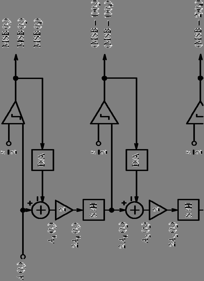
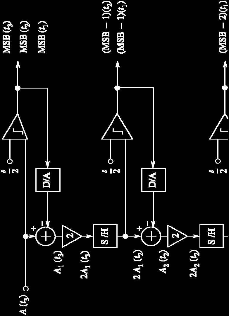
54 Residue converter parameters The residue ADC uses, for each bit One comparator (for bit value decision) One 1-bit DAC (to build the approximation) One (analog) adder (to evaluate the residue) One amplifier (gain = 2) (to bring residue to full scale) 12/05/ ATLCE - D DDC
55 Block diagram of residue ADC or 12/05/ ATLCE - D DDC
56 Precision in subranging converters Any error in residue evaluation is propagated to the following stages residue must be evaluated with a resolution corresponding to the residual bit number» ADC precision» DAC precision» Amplifiers and S/H (pipeline) precision Previous example First stage ADC and DAC (1-bit) need 8-bit precision precision decreases towards LSBs 12/05/ ATLCE - D DDC
57 Subranging ADC parameters N comparators N comparison cycles for N-bit conversion Vs successive approximation ADC Higher complexity: N vs 1 comparator Same speed: N steps No benefit Useful as starting structure for pipeline ADC 12/05/ ATLCE - D DDC
58 Lesson D3: A/D converters Analog to Digital converters Error taxonomy (linear, nonlinear, dynamic) Converter parameters: complexity and speed Examples of A/D converters Flash, Tracking Successive approximation, Residue/subranging Pipeline structures Performance tradeoff 12/05/ ATLCE - D DDC
59 Multistage pipeline converters Operate on different samples at the same time Input sample 1 Input sample 2, processa 1 Input sample 3, processa 2, processb 1.. ProcessZ 1. Output sample 1 Needs analog memory elements 12/05/ ATLCE - D DDC
60 Pipeline sequence Input sample sequence: A, B, C, D,... Processing stage time t1 t2 t3 t4 1 A B C D 2 X A B C 3 X X A B 4 X X X A result of sample A conversion available 12/05/ ATLCE - D DDC
61 Pipeline-subranging ADC 12/05/ ATLCE - D DDC
62 Comparison with other techniques A N-bit pipeline A/D converter uses: N comparators N comparison cycles (to complete the conversion of each sample) Conversion time: N-cycle latency 1-cycle conversion (throughput) Same speed as a flash with N comparators (2 N in the flash) 12/05/ ATLCE - D DDC
63 Speed vs complexity Complex Conv time Latency Parallel (flash) 2 N 1 1 Pipeline N 1 N Residue N N N Successive Approx 1 N N Tracking 1 2 N 2 N Complexity: Conversion time: Latency: proportional to the number of comparators. the maximum number of comparator delay (clock periods) to complete a conversion delay to get the result. 12/05/ ATLCE - D DDC
64 Classic 8-bit converters 8-bit Flash: = 255 comparators; T CT = T C 8-bit SAR: 1 comparator; T CT = 8 T C + 7 T DA Limited choice No room for tradeoff Can we do something between? Faster than SAR, slower than flash Less expensive than flash (less comparators) 12/05/ ATLCE - D DDC
65 Example: best cost/speed architecture Goal: 8-bit ADC Conversion time Tct < 60 ns Devices available: comparators with Tc = 10 ns Suitable design SAR: conversion time Tc = 8 x 10 = 80 ns too long Flash: Tc = 10 ns, but» Expensive: 255 comparators» Overkilling: 60 ns is enough Any other choice? 12/05/ ATLCE - D DDC
66 Multibit residue architectures First-stage conversion on 1, 2, 3, M bits Comparators are replaced by M-bit ADC The approximation is built using M-bit DAC Residue has a max value Ad = S/ 2 M Gain required to bring residue up to S: 2 M Multibit-residue provides various speed/complexity tradeoffs Higher speed, with the same number of comparators Less comparators for the same speed Better tuning of design to specifications 12/05/ ATLCE - D DDC
67 Choices for 8-bit converters Comparators, conversion time (T CT ), latency (T L ) 8-bit Flash: = 255 comparators; T CT = T C T L = 1 8-bit SAR: 1 comparator; T CT = 8 T C + 7 T DA T L = 8 Something in the middle: multibit residue subranging converters Two cascaded 4-bit flash: 2(2 4-1) = 30 comparators; T CT = 2T C +T DA T L = 2 Four cascaded 2-bit flash: 4(2 2-1) = 12 comparators; T CT = 4T C + 3 T DA T L = 4 12/05/ ATLCE - D DDC
68 Multibit residue ADC: 2 4-bit cells A/D - 4bit + 16 D/A - 4bit MSB,.. (D7, 6, 5, 4) 8-bit residue ADC: 2 4-bit cells Total conversion time: Tc = 2 x Tc(A/D) + Ta(D/A) A/D - 4bit D3, 2, 1, 0 12/05/ ATLCE - D DDC
69 Multibit residue ADC: 4 2-bit cells A/D - 2bit + 4 D/A - 2bit MSB, MSB-1 (D7, D6) 8-bit residue ADC: 4 2-bit cells Total conversion time Tct = 4 x Tc(A/D) + 3 x Ta(D/A) A/D - 2bit D5, D4 + D/A - 2bit 4 A/D - 2bit D3, D2 + 4 D/A - 2bit A/D - 2bit LSB+1, LSB (D1, D0) 12/05/ ATLCE - D DDC
70 Multibit residue ADC comparison A/D - 4bit + 16 D/A - 4bit MSB,.. (D7, 6, 5, 4) A/D - 2bit + 4 D/A - 2bit MSB, MSB-1 (D7, D6) A/D - 4bit D3, 2, 1, 0 A/D - 2bit D5, D4 8-bit residue ADC: 2 4-bit cells Tct = 2 x Tc(A/D) + Ta(D/A) + 4 D/A - 2bit A/D - 2bit D3, D2 + D/A - 2bit 8-bit residue ADC: 4 2-bit cells Tct = 4 x Tc(A/D) + 3 x Ta(D/A) 4 A/D - 2bit LSB+1, LSB (D1, D0) 12/05/ ATLCE - D DDC
71 Speed vs complexity with multibit Complex Speed Conv time Latency Parallel (flash) 2 N 1 1 Pipeline N 1 N Residue N N N Residue K bit N/K N/K N Successive Approx 1 N N Tracking 1 2 N 2 N. 12/05/ ATLCE - D DDC
72 Mixed and multistage converters Application of subranging to bit groups (K-bit) Comparator N bit ADC Residue evaluation N bit DAC + differential amplifier With K-bit groups N/K stages Interstage amplifier gain 2 N Basic ADC: FLASH Complexity: Ps = 2 K total: P T = N/K x 2 K Conversion time T C = 1 total: T CT = N/K x T C Basic ADC: SAR Complexity: Ps = 1 total: P T = N/K Conversion time T C = K total: T CT = N x T C 12/05/ ATLCE - D DDC
73 Pipeline converters Pipeline can be usd for any multistage Reduces the equivalent conversion time T CT Faster equivalent conversion rate F S Same latency time Pipeline = Residue + Memory element (analog) at the input of each stage Change each amplifier into Sample/Hold + amplifier Some added complexity Multibit residue pipeline FLASH ADC: equivalent T CT = 1 (more precisely T C +T DA ) SAR ADC: equivalent T CT = K T C (more precisely K (T C +T DA )) Additional design freedom 12/05/ ATLCE - D DDC
74 Speed vs complexity with multibit Complex Speed Conv time Latency Parallel (flash) 2 N 1 1 Pipeline N 1 N Residue N N N Residue K bit Flash (2 K )N/K N/K 1 Residue K bit SAR N/K N N Successive Approx 1 N N Tracking 1 2 N 2 N. 12/05/ ATLCE - D DDC
75 Speed vs complexity - graph Complexity (log) 2 N Flash N Pipeline Residue 1 SAR 1 N 2 N Tracking Conversion time (log). 12/05/ ATLCE - D DDC
76 Choices for 12-bit residue ADC Complexity (log) Residue 12x1 (Flash) Residue 6x2 <bit/stage>x<num stage> Residue 4x3 Residue 3x4 Residue 2x6 Residue 1x > Conv. time. 12/05/ ATLCE - D DDC
77 Telecom applications ADC Direct RF or IF signal conversion Parameters dynamic range (resolution, bit number) conversion rate (1/Tc) linearity (THD) full power bandwidth spurious free dynamic range (SFDR) signal/(noise+distortion) ratio (SINAD) 12/05/ ATLCE - D DDC
78 Lab experiment Operation and errors of a D/A converter D/A converter with weighted resistors or ladder network, voltage switches, voltage output. Driving with CMOS logic circuits (counter) Measurement of A(D) Evaluation of approximating straight line Gain, offset, nonlinearity errors Conversion in tracking ADC Dynamic range and slew rate verification Text reference sect. 4.L1 12/05/ ATLCE - D DDC
79 Lesson D3 - final test Which is the effect of strong differential nonlinearity error? Describe the missed-code error. Which parameters can be used to classify ADCs? Draw the block diagram of a residue/subranging converter. Explain the difference between conversion time and latency. How many comparators are required for a 8-bit flash ADC? Which is the conversion delay (as number of comparator decision times) for a 8-bit SAR ADC? Draw the block diagram of a residue converter using 3 stages, with 3 bits each. 12/05/ ATLCE - D DDC
Analog and Telecommunication Electronics
 Politecnico di Torino Electronic Eng. Master Degree Analog and Telecommunication Electronics D2 - DAC taxonomy and errors» Static and dynamic parameters» DAC taxonomy» DAC circuits» Error sources AY 2015-16
Data Converter Fundamentals
 Data Converter Fundamentals David Johns and Ken Martin (johns@eecg.toronto.edu) (martin@eecg.toronto.edu) slide 1 of 33 Introduction Two main types of converters Nyquist-Rate Converters Generate output
Pipelined multi step A/D converters
 Department of Electrical Engineering Indian Institute of Technology, Madras Chennai, 600036, India 04 Nov 2006 Motivation for multi step A/D conversion Flash converters: Area and power consumption increase
Slide Set Data Converters. Digital Enhancement Techniques
 0 Slide Set Data Converters Digital Enhancement Techniques Introduction Summary Error Measurement Trimming of Elements Foreground Calibration Background Calibration Dynamic Matching Decimation and Interpolation
Chapter 5. Digital Design and Computer Architecture, 2 nd Edition. David Money Harris and Sarah L. Harris. Chapter 5 <1>
 Chapter 5 Digital Design and Computer Architecture, 2 nd Edition David Money Harris and Sarah L. Harris Chapter 5 Chapter 5 :: Topics Introduction Arithmetic Circuits umber Systems Sequential Building
Summary Last Lecture
 EE247 Lecture 19 ADC Converters Sampling (continued) Sampling switch charge injection & clock feedthrough Complementary switch Use of dummy device Bottom-plate switching Track & hold T/H circuits T/H combined
D/A Converters. D/A Examples
 D/A architecture examples Unit element Binary weighted Static performance Component matching Architectures Unit element Binary weighted Segmented Dynamic element matching Dynamic performance Glitches Reconstruction
EE 435. Lecture 26. Data Converters. Data Converter Characterization
 EE 435 Lecture 26 Data Converters Data Converter Characterization . Review from last lecture. Data Converter Architectures Large number of different circuits have been proposed for building data converters
Digital Signal 2 N Most Significant Bit (MSB) Least. Bit (LSB)
 Least. Bit (LSB)") 1 Digital Signal Binary or two stages: 0 (Low voltage 0-3 V) 1 (High voltage 4-5 V) Binary digit is called bit. Group of bits is called word. 8-bit group is called byte. For N-bit base-2 number = 2 N levels
1 Digital Signal Binary or two stages: 0 (Low voltage 0-3 V) 1 (High voltage 4-5 V) Binary digit is called bit. Group of bits is called word. 8-bit group is called byte. For N-bit base-2 number = 2 N levels
Digital Electronic Meters
 Digital Electronic Meters EIE 240 Electrical and Electronic Measurement May 1, 2015 1 Digital Signal Binary or two stages: 0 (Low voltage 0-3 V) 1 (High voltage 4-5 V) Binary digit is called bit. Group
Lecture 340 Characterization of DACs and Current Scaling DACs (5/1/10) Page 340-1
 Page 340-1") Lecture 34 Characterization of DACs and Current Scaling DACs (5//) Page 34 LECTURE 34 CHARACTERZATON OF DACS AND CURRENT SCALNG DACS LECTURE ORGANZATON Outline ntroduction Static characterization of DACs
Lecture 34 Characterization of DACs and Current Scaling DACs (5//) Page 34 LECTURE 34 CHARACTERZATON OF DACS AND CURRENT SCALNG DACS LECTURE ORGANZATON Outline ntroduction Static characterization of DACs
Lecture 10, ATIK. Data converters 3
 Lecture, ATIK Data converters 3 What did we do last time? A quick glance at sigma-delta modulators Understanding how the noise is shaped to higher frequencies DACs A case study of the current-steering
EE 435. Lecture 26. Data Converters. Data Converter Characterization
 EE 435 Lecture 26 Data Converters Data Converter Characterization . Review from last lecture. Data Converter Architectures n DAC R-2R (4-bits) R R R R V OUT 2R 2R 2R 2R R d 3 d 2 d 1 d 0 V REF By superposition:
S.Y. Diploma : Sem. III [DE/ED/EI/EJ/EN/ET/EV/EX/IC/IE/IS/IU/MU] Principles of Digital Techniques
![S.Y. Diploma : Sem. III [DE/ED/EI/EJ/EN/ET/EV/EX/IC/IE/IS/IU/MU] Principles of Digital Techniques](/thumbs/82/86792063.jpg "S.Y. Diploma : Sem. III [DE/ED/EI/EJ/EN/ET/EV/EX/IC/IE/IS/IU/MU] Principles of Digital Techniques") S.Y. Diploma : Sem. III [DE/ED/EI/EJ/EN/ET/EV/EX/IC/IE/IS/IU/MU] Principles of Digital Techniques Time: 3 Hrs.] Prelim Question Paper Solution [Marks : 100 Q.1(a) Attempt any SIX of the following : [12]
S.Y. Diploma : Sem. III [DE/ED/EI/EJ/EN/ET/EV/EX/IC/IE/IS/IU/MU] Principles of Digital Techniques Time: 3 Hrs.] Prelim Question Paper Solution [Marks : 100 Q.1(a) Attempt any SIX of the following : [12]
EE247 Lecture 16. Serial Charge Redistribution DAC
 EE47 Lecture 16 D/A Converters D/A examples Serial charge redistribution DAC Practical aspects of current-switch DACs Segmented current-switch DACs DAC self calibration techniques Current copiers Dynamic
MAHARASHTRA STATE BOARD OF TECHNICAL EDUCATION (Autonomous) (ISO/IEC Certified) SUMMER 14 EXAMINATION Model Answer
 (ISO/IEC Certified) SUMMER 14 EXAMINATION Model Answer") MAHARASHTRA STATE BOARD OF TECHNICAL EDUCATION (Autonomous) (ISO/IEC 27001 2005 Certified) SUMMER 14 EXAMINATION Model Answer Subject Code : 17320 Page No: 1/34 Important Instructions to examiners: 1)
MAHARASHTRA STATE BOARD OF TECHNICAL EDUCATION (Autonomous) (ISO/IEC 27001 2005 Certified) SUMMER 14 EXAMINATION Model Answer Subject Code : 17320 Page No: 1/34 Important Instructions to examiners: 1)
A novel Capacitor Array based Digital to Analog Converter
 Chapter 4 A novel Capacitor Array based Digital to Analog Converter We present a novel capacitor array digital to analog converter(dac architecture. This DAC architecture replaces the large MSB (Most Significant
A Gray Code Based Time-to-Digital Converter Architecture and its FPGA Implementation
 A Gray Code Based Time-to-Digital Converter Architecture and its FPGA Implementation Congbing Li Haruo Kobayashi Gunma University Gunma University Kobayashi Lab Outline Research Objective & Background
EE 435. Lecture 36. Quantization Noise ENOB Absolute and Relative Accuracy DAC Design. The String DAC
 EE 435 Lecture 36 Quantization Noise ENOB Absolute and elative Accuracy DAC Design The String DAC . eview from last lecture. Quantization Noise in ADC ecall: If the random variable f is uniformly distributed
MAHARASHTRA STATE BOARD OF TECHNICAL EDUCATION (Autonomous) (ISO/IEC Certified)
 (ISO/IEC Certified)") WINTER 17 EXAMINATION Subject Name: Digital Techniques Model Answer Subject Code: 17333 Important Instructions to examiners: 1) The answers should be examined by key words and not as word-to-word as given
WINTER 17 EXAMINATION Subject Name: Digital Techniques Model Answer Subject Code: 17333 Important Instructions to examiners: 1) The answers should be examined by key words and not as word-to-word as given
on candidate s understanding. 7) For programming language papers, credit may be given to any other program based on equivalent concept.
 For programming language papers, credit may be given to any other program based on equivalent concept.") WINTER 17 EXAMINATION Subject Name: Digital Techniques Model Answer Subject Code: 17333 Important Instructions to examiners: 1) The answers should be examined by key words and not as word-to-word as given
WINTER 17 EXAMINATION Subject Name: Digital Techniques Model Answer Subject Code: 17333 Important Instructions to examiners: 1) The answers should be examined by key words and not as word-to-word as given
EXTENDING THE RESOLUTION OF PARALLEL DIGITAL-ANALOG CONVERTERS
 CMOS Analog IC Design Page 10.3-1 10.3 - EXTENDING THE RESOLUTION OF PARALLEL DIGITAL-ANALOG CONVERTERS TECHNIQUE: Divide the total resolution N into k smaller sub-dacs each with a resolution of N k. Result:
PARALLEL DIGITAL-ANALOG CONVERTERS
 CMOS Analog IC Design Page 10.2-1 10.2 - PARALLEL DIGITAL-ANALOG CONVERTERS CLASSIFICATION OF DIGITAL-ANALOG CONVERTERS CMOS Analog IC Design Page 10.2-2 CURRENT SCALING DIGITAL-ANALOG CONVERTERS GENERAL
MAHARASHTRA STATE BOARD OF TECHNICAL EDUCATION (Autonomous) (ISO/IEC Certified) State any two Boolean laws. (Any 2 laws 1 mark each)
 (ISO/IEC Certified) State any two Boolean laws. (Any 2 laws 1 mark each)") Subject Code: 17333 Model Answer Page 1/ 27 Important Instructions to examiners: 1) The answers should be examined by key words and not as word-to-word as given in the model answer scheme. 2) The model
Subject Code: 17333 Model Answer Page 1/ 27 Important Instructions to examiners: 1) The answers should be examined by key words and not as word-to-word as given in the model answer scheme. 2) The model
Nyquist-Rate D/A Converters. D/A Converter Basics.
 Nyquist-Rate D/A Converters David Johns and Ken Martin (johns@eecg.toronto.edu) (martin@eecg.toronto.edu) slide 1 of 20 D/A Converter Basics. B in D/A is a digital signal (or word), B in b i B in = 2 1
EE 521: Instrumentation and Measurements
 Aly El-Osery Electrical Engineering Department, New Mexico Tech Socorro, New Mexico, USA September 23, 2009 1 / 18 1 Sampling 2 Quantization 3 Digital-to-Analog Converter 4 Analog-to-Digital Converter
Sample Test Paper - I
 Scheme G Sample Test Paper - I Course Name : Computer Engineering Group Marks : 25 Hours: 1 Hrs. Q.1) Attempt any THREE: 09 Marks a) Define i) Propagation delay ii) Fan-in iii) Fan-out b) Convert the following:
Successive Approximation ADCs
 Department of Electrical and Computer Engineering Successive Approximation ADCs Vishal Saxena Vishal Saxena -1- Successive Approximation ADC Vishal Saxena -2- Data Converter Architectures Resolution [Bits]
Digital to Analog Converters I
 Advanced Analog Building Blocks 2 Digital to Analog Converters I Albert Comerma (PI) (comerma@physi.uni-heidelberg.de) Course web WiSe 2017 DAC parameters DACs parameters DACs non ideal effects DACs performance
Measurement and Instrumentation. Sampling, Digital Devices, and Data Acquisition
 2141-375 Measurement and Instrumentation Sampling, Digital Devices, and Data Acquisition Basic Data Acquisition System Analog Form Analog Form Digital Form Display Physical varialble Sensor Signal conditioning
EE 435. Lecture 26. Data Converters. Differential Nonlinearity Spectral Performance
 EE 435 Lecture 26 Data Converters Differential Nonlinearity Spectral Performance . Review from last lecture. Integral Nonlinearity (DAC) Nonideal DAC INL often expressed in LSB INL = X k INL= max OUT OF
Analog and Telecommunication Electronics
 Politecnico di Torino - ICT School Analog and Telecommunication Electronics B6 - Non-linear circuits» Nonlinear circuits taxonomy» Log amplifiers: Error sources» Ratiometric, bipolar circuits» Saturating
LOGIC CIRCUITS. Basic Experiment and Design of Electronics. Ho Kyung Kim, Ph.D.
 Basic Experiment and Design of Electronics LOGIC CIRCUITS Ho Kyung Kim, Ph.D. hokyung@pusan.ac.kr School of Mechanical Engineering Pusan National University Digital IC packages TTL (transistor-transistor
S.Y. Diploma : Sem. III [CO/CM/IF/CD/CW] Digital Techniques
![S.Y. Diploma : Sem. III [CO/CM/IF/CD/CW] Digital Techniques](/thumbs/90/103932933.jpg "S.Y. Diploma : Sem. III [CO/CM/IF/CD/CW] Digital Techniques") S.Y. Diploma : Sem. III [CO/CM/IF/CD/CW] Digital Techniques Time: 3 Hrs.] Prelim Question Paper Solution [Marks : 100 Q.1(a) Attempt any SIX of the following : [12] Q.1(a) (i) Derive AND gate and OR gate
S.Y. Diploma : Sem. III [CO/CM/IF/CD/CW] Digital Techniques Time: 3 Hrs.] Prelim Question Paper Solution [Marks : 100 Q.1(a) Attempt any SIX of the following : [12] Q.1(a) (i) Derive AND gate and OR gate
Lab 3 Revisited. Zener diodes IAP 2008 Lecture 4 1
 Lab 3 Revisited Zener diodes R C 6.091 IAP 2008 Lecture 4 1 Lab 3 Revisited +15 Voltage regulators 555 timers 270 1N758 0.1uf 5K pot V+ V- 2N2222 0.1uf V o. V CC V Vin s = 5 V Vc V c Vs 1 e t = RC Threshold
Nyquist-Rate A/D Converters
 IsLab Analog Integrated ircuit Design AD-51 Nyquist-ate A/D onverters כ Kyungpook National University IsLab Analog Integrated ircuit Design AD-1 Nyquist-ate MOS A/D onverters Nyquist-rate : oversampling
Pipelined A/D Converters
 EE247 Lecture 2 AC Converters Pipelined ACs EECS 247 Lecture 2: ata Converters 24 H.K. Page Pipelined A/ Converters Ideal operation Errors and correction Redundancy igital calibration Implementation Practical
LOGIC CIRCUITS. Basic Experiment and Design of Electronics
 Basic Experiment and Design of Electronics LOGIC CIRCUITS Ho Kyung Kim, Ph.D. hokyung@pusan.ac.kr School of Mechanical Engineering Pusan National University Outline Combinational logic circuits Output
EEO 401 Digital Signal Processing Prof. Mark Fowler
 EEO 401 Digital Signal Processing Pro. Mark Fowler Note Set #14 Practical A-to-D Converters and D-to-A Converters Reading Assignment: Sect. 6.3 o Proakis & Manolakis 1/19 The irst step was to see that
Analog to Digital Converters (ADCs)
") Analog to Digital Converters (ADCs) Note: Figures are copyrighted Proakis & Manolakis, Digital Signal Processing, 4 th Edition, Pearson Publishers. Embedded System Design A Unified HW Approach, Vahid/Givargis,
Analog to Digital Converters (ADCs) Note: Figures are copyrighted Proakis & Manolakis, Digital Signal Processing, 4 th Edition, Pearson Publishers. Embedded System Design A Unified HW Approach, Vahid/Givargis,
I. Motivation & Examples
 I. Motivation & Examples Output depends on current input and past history of inputs. State embodies all the information about the past needed to predict current output based on current input. State variables,
SUMMER 18 EXAMINATION Subject Name: Principles of Digital Techniques Model Answer Subject Code:
 Important Instructions to examiners: 1) The answers should be examined by key words and not as word-to-word as given in the model answer scheme. 2) The model answer and the answer written by candidate
Digital Fundamentals
 Digital Fundamentals Tenth Edition Floyd Chapter 9 Sections 9-1 thru 9-5 2009 Pearson Education, Upper 2008 Pearson Saddle River, Education NJ 07458. All Rights Reserved ET285 Agenda Week 2 Quiz 0: Covered
ENGG 1203 Tutorial _03 Laboratory 3 Build a ball counter. Lab 3. Lab 3 Gate Timing. Lab 3 Steps in designing a State Machine. Timing diagram of a DFF
 ENGG 1203 Tutorial _03 Laboratory 3 Build a ball counter Timing diagram of a DFF Lab 3 Gate Timing difference timing for difference kind of gate, cost dependence (1) Setup Time = t2-t1 (2) Propagation
Design of Sequential Circuits
 Design of Sequential Circuits Seven Steps: Construct a state diagram (showing contents of flip flop and inputs with next state) Assign letter variables to each flip flop and each input and output variable
INSTRUMENTAL ENGINEERING
 INSTRUMENTAL ENGINEERING Subject Code: IN Course Structure Sections/Units Section A Unit 1 Unit 2 Unit 3 Unit 4 Unit 5 Unit 6 Section B Section C Section D Section E Section F Section G Section H Section
ECEN 610 Mixed-Signal Interfaces
 ECEN 610 Mixed-Signal Interfaces Sebastian Hoyos Texas A&M University Analog and Mixed Signal Group Spring 014 S. Hoyos-ECEN-610 1 Sample-and-Hold Spring 014 S. Hoyos-ECEN-610 ZOH vs. Track-and-Hold V(t)
! Charge Leakage/Charge Sharing. " Domino Logic Design Considerations. ! Logic Comparisons. ! Memory. " Classification. " ROM Memories.
 ESE 57: Digital Integrated Circuits and VLSI Fundamentals Lec 9: March 9, 8 Memory Overview, Memory Core Cells Today! Charge Leakage/ " Domino Logic Design Considerations! Logic Comparisons! Memory " Classification
EE 435. Lecture 28. Data Converters Linearity INL/DNL Spectral Performance
 EE 435 Lecture 8 Data Converters Linearity INL/DNL Spectral Performance Performance Characterization of Data Converters Static characteristics Resolution Least Significant Bit (LSB) Offset and Gain Errors
Logic Design II (17.342) Spring Lecture Outline
 Spring Lecture Outline") Logic Design II (17.342) Spring 2012 Lecture Outline Class # 10 April 12, 2012 Dohn Bowden 1 Today s Lecture First half of the class Circuits for Arithmetic Operations Chapter 18 Should finish at least
Logic Design II (17.342) Spring 2012 Lecture Outline Class # 10 April 12, 2012 Dohn Bowden 1 Today s Lecture First half of the class Circuits for Arithmetic Operations Chapter 18 Should finish at least
Oversampling Converters
 Oversampling Converters David Johns and Ken Martin (johns@eecg.toronto.edu) (martin@eecg.toronto.edu) slide 1 of 56 Motivation Popular approach for medium-to-low speed A/D and D/A applications requiring
ESE 570: Digital Integrated Circuits and VLSI Fundamentals
 ESE 570: Digital Integrated Circuits and VLSI Fundamentals Lec 19: March 29, 2018 Memory Overview, Memory Core Cells Today! Charge Leakage/Charge Sharing " Domino Logic Design Considerations! Logic Comparisons!
MODEL ANSWER SUMMER 17 EXAMINATION Subject Title: Principles of Digital Techniques
 MODEL ANSWER SUMMER 17 EXAMINATION Subject Title: Principles of Digital Techniques Subject Code: Important Instructions to examiners: 1) The answers should be examined by key words and not as word-to-word
A Nonuniform Quantization Scheme for High Speed SAR ADC Architecture
 A Nonuniform Quantization Scheme for High Speed SAR ADC Architecture Youngchun Kim Electrical and Computer Engineering The University of Texas Wenjuan Guo Intel Corporation Ahmed H Tewfik Electrical and
Extremely small differential non-linearity in a DMOS capacitor based cyclic ADC for CMOS image sensors
 Extremely small differential non-linearity in a DMOS capacitor based cyclic ADC for CMOS image sensors Zhiheng Wei 1a), Keita Yasutomi ) and Shoji Kawahito b) 1 Graduate School of Science and Technology,
Successive approximation time-to-digital converter based on vernier charging method
 LETTER Successive approximation time-to-digital converter based on vernier charging method Xin-Gang Wang 1, 2, Hai-Gang Yang 1a), Fei Wang 1, and Hui-He 2 1 Institute of Electronics, Chinese Academy of
CHW 261: Logic Design
 CHW 26: Logic Design Instructors: Prof. Hala Zayed Dr. Ahmed Shalaby http://www.bu.edu.eg/staff/halazayed4 http://bu.edu.eg/staff/ahmedshalaby4# Slide Digital Fundamentals CHAPTER 8 Counters Slide 2 Counting
Digital Fundamentals
 Digital Fundamentals Tenth Edition Floyd hapter 8 Modified by Yuttapong Jiraraksopakun Floyd, Digital Fundamentals, 10 th 2008 Pearson Education ENE, KMUTT ed 2009 ounting in Binary As you know, the binary
Sequential Logic Circuits
 Chapter 4 Sequential Logic Circuits 4 1 The defining characteristic of a combinational circuit is that its output depends only on the current inputs applied to the circuit. The output of a sequential circuit,
EE 435. Lecture 29. Data Converters. Linearity Measures Spectral Performance
 EE 435 Lecture 9 Data Converters Linearity Measures Spectral Performance Linearity Measurements (testing) Consider ADC V IN (t) DUT X IOUT V REF Linearity testing often based upon code density testing
Latches. October 13, 2003 Latches 1
 Latches The second part of CS231 focuses on sequential circuits, where we add memory to the hardware that we ve already seen. Our schedule will be very similar to before: We first show how primitive memory
Digital Circuits, Binary Numbering, and Logic Gates Cornerstone Electronics Technology and Robotics II
 Digital Circuits, Binary Numbering, and Logic Gates Cornerstone Electronics Technology and Robotics II Administration: o Prayer Electricity and Electronics, Section 20.1, Digital Fundamentals: o Fundamentals:
MASSACHUSETTS INSTITUTE OF TECHNOLOGY Department of Electrical Engineering and Computer Sciences
 MASSACHUSETTS INSTITUTE OF TECHNOLOGY Department of Electrical Engineering and Computer Sciences Analysis and Design of Digital Integrated Circuits (6.374) - Fall 2003 Quiz #2 Prof. Anantha Chandrakasan
Up/down binary counter with separate up/down clocks
 FEATURES Synchronous reversible 4-bit counting Asynchronous parallel load capability Asynchronous reset (clear) Cascadable without external logic DESCRIPTION The is a 4-bit synchronous up/down counter
ELECTRONIC SYSTEMS. Basic operational amplifier circuits. Electronic Systems - C3 13/05/ DDC Storey 1
 Electronic Systems C3 3/05/2009 Politecnico di Torino ICT school Lesson C3 ELECTONIC SYSTEMS C OPEATIONAL AMPLIFIES C.3 Op Amp circuits» Application examples» Analysis of amplifier circuits» Single and
Chapter Overview. Memory Classification. Memory Architectures. The Memory Core. Periphery. Reliability. Memory
 SRAM Design Chapter Overview Classification Architectures The Core Periphery Reliability Semiconductor Classification RWM NVRWM ROM Random Access Non-Random Access EPROM E 2 PROM Mask-Programmed Programmable
EE100Su08 Lecture #9 (July 16 th 2008)
") EE100Su08 Lecture #9 (July 16 th 2008) Outline HW #1s and Midterm #1 returned today Midterm #1 notes HW #1 and Midterm #1 regrade deadline: Wednesday, July 23 rd 2008, 5:00 pm PST. Procedure: HW #1: Bart
EE100Su08 Lecture #9 (July 16 th 2008) Outline HW #1s and Midterm #1 returned today Midterm #1 notes HW #1 and Midterm #1 regrade deadline: Wednesday, July 23 rd 2008, 5:00 pm PST. Procedure: HW #1: Bart
DAC10* PRODUCT PAGE QUICK LINKS Last Content Update: 02/23/2017
 * PRODUCT PAGE QUICK LINKS Last Content Update: 0/3/07 COMPARABLE PARTS View a parametric search of comparable parts. DOCUMENTATION Data Sheet : 0-Bit Current-Out DAC Data Sheet REFERENCE MATERIALS Solutions
Random Number Generator Digital Design - Demo
 Understanding Digital Design The Digital Electronics 2014 Digital Design - Demo This presentation will Review the oard Game Counter block diagram. Review the circuit design of the sequential logic section
Digital Integrated Circuits A Design Perspective
 Semiconductor Memories Adapted from Chapter 12 of Digital Integrated Circuits A Design Perspective Jan M. Rabaey et al. Copyright 2003 Prentice Hall/Pearson Outline Memory Classification Memory Architectures
Lecture 4. Adders. Computer Systems Laboratory Stanford University
 Lecture 4 Adders Computer Systems Laboratory Stanford University horowitz@stanford.edu Copyright 2006 Mark Horowitz Some figures from High-Performance Microprocessor Design IEEE 1 Overview Readings Today
Mark Redekopp, All rights reserved. Lecture 1 Slides. Intro Number Systems Logic Functions
 Lecture Slides Intro Number Systems Logic Functions EE 0 in Context EE 0 EE 20L Logic Design Fundamentals Logic Design, CAD Tools, Lab tools, Project EE 357 EE 457 Computer Architecture Using the logic
Chapter 4. Sequential Logic Circuits
 Chapter 4 Sequential Logic Circuits 1 2 Chapter 4 4 1 The defining characteristic of a combinational circuit is that its output depends only on the current inputs applied to the circuit. The output of
WORKBOOK. Try Yourself Questions. Electrical Engineering Digital Electronics. Detailed Explanations of
 27 WORKBOOK Detailed Eplanations of Try Yourself Questions Electrical Engineering Digital Electronics Number Systems and Codes T : Solution Converting into decimal number system 2 + 3 + 5 + 8 2 + 4 8 +
EE40 Lec 15. Logic Synthesis and Sequential Logic Circuits
 EE40 Lec 15 Logic Synthesis and Sequential Logic Circuits Prof. Nathan Cheung 10/20/2009 Reading: Hambley Chapters 7.4-7.6 Karnaugh Maps: Read following before reading textbook http://www.facstaff.bucknell.edu/mastascu/elessonshtml/logic/logic3.html
The influence of parasitic capacitors on SAR ADC characteristics
 The influence of parasitic capacitors on SAR ADC characteristics DMITRY NORMANOV, DMITRY OSIPOV National Research Nuclear University MEPHI ASIC Lab 59, Moscow, Kashirskoe shosse, 3 RUSSIA simplere@ya.ru
ir. Georgi Radulov 1, dr. ir. Patrick Quinn 2, dr. ir. Hans Hegt 1, prof. dr. ir. Arthur van Roermund 1 Eindhoven University of Technology Xilinx
 Calibration of Current Steering D/A Converters ir. eorgi Radulov 1, dr. ir. Patrick Quinn 2, dr. ir. Hans Hegt 1, prof. dr. ir. Arthur van Roermund 1 1 Eindhoven University of Technology 2 Xilinx Current-steering
EE241 - Spring 2000 Advanced Digital Integrated Circuits. References
 EE241 - Spring 2000 Advanced Digital Integrated Circuits Lecture 26 Memory References Rabaey, Digital Integrated Circuits Memory Design and Evolution, VLSI Circuits Short Course, 1998.» Gillingham, Evolution
Experimental Verification of a Timing Measurement Circuit With Self-Calibration
 19 th IEEE IMS3TW, Porto Alegre, Brazil Sept. 17, 2014 Experimental Verification of a Timing Measurement Circuit With Self-Calibration Kateshi Chujyo, Daiki Hirabayashi, Kentaroh Katoh Conbing Li, Yutaroh
On the design of Incremental ΣΔ Converters
 M. Belloni, C. Della Fiore, F. Maloberti, M. Garcia Andrade: "On the design of Incremental ΣΔ Converters"; IEEE Northeast Workshop on Circuits and Sstems, NEWCAS 27, Montreal, 5-8 August 27, pp. 376-379.
ELEC Digital Logic Circuits Fall 2014 Sequential Circuits (Chapter 6) Finite State Machines (Ch. 7-10)
 Finite State Machines (Ch. 7-10)") ELEC 2200-002 Digital Logic Circuits Fall 2014 Sequential Circuits (Chapter 6) Finite State Machines (Ch. 7-10) Vishwani D. Agrawal James J. Danaher Professor Department of Electrical and Computer Engineering
ELEC 2200-002 Digital Logic Circuits Fall 2014 Sequential Circuits (Chapter 6) Finite State Machines (Ch. 7-10) Vishwani D. Agrawal James J. Danaher Professor Department of Electrical and Computer Engineering
Research Article Linearity Analysis on a Series-Split Capacitor Array for High-Speed SAR ADCs
 Hindawi Publishing Corporation LSI Design olume 1, Article ID 76548, 8 pages doi:1.1155/1/76548 Research Article Linearity Analysis on a Series-Split Capacitor Array for High-Speed SAR ADCs Yan Zhu, 1
INTEGRATED CIRCUITS. For a complete data sheet, please also download:
 INTEGRATED CIRCUITS DATA SHEET For a complete data sheet, please also download: The IC6 74HC/HCT/HCU/HCMOS ogic Family Specifications The IC6 74HC/HCT/HCU/HCMOS ogic Package Information The IC6 74HC/HCT/HCU/HCMOS
King Fahd University of Petroleum and Minerals College of Computer Science and Engineering Computer Engineering Department
 King Fahd University of Petroleum and Minerals College of Computer Science and Engineering Computer Engineering Department Page of COE 22: Digital Logic Design (3--3) Term (Fall 22) Final Exam Sunday January
Looking at a two binary digit sum shows what we need to extend addition to multiple binary digits.
 A Full Adder The half-adder is extremely useful until you want to add more that one binary digit quantities. The slow way to develop a two binary digit adders would be to make a truth table and reduce
EECS150 - Digital Design Lecture 23 - FSMs & Counters
 EECS150 - Digital Design Lecture 23 - FSMs & Counters April 8, 2010 John Wawrzynek Spring 2010 EECS150 - Lec22-counters Page 1 One-hot encoding of states. One FF per state. State Encoding Why one-hot encoding?
SHM-14 Ultra-Fast, 14-Bit Linear Monolithic Sample-Hold Amplifiers
 INNOVATION and EX C ELL E N C E Ultra-Fast, 1-Bit Linear Monolithic Sample-Hold Amplifiers FEATURES Fast acquisition time: 10ns to ±0.1% 0ns to ±0.0% ns to ±0.01% ±0.001% Nonlinearity 6µV rms output noise
Pipelined Viterbi Decoder Using FPGA
 Research Journal of Applied Sciences, Engineering and Technology 5(4): 1362-1372, 2013 ISSN: 2040-7459; e-issn: 2040-7467 Maxwell Scientific Organization, 2013 Submitted: July 05, 2012 Accepted: August
10/12/2016. An FSM with No Inputs Moves from State to State. ECE 120: Introduction to Computing. Eventually, the States Form a Loop
 University of Illinois at Urbana-Champaign Dept. of Electrical and Computer Engineering An FSM with No Inputs Moves from State to State What happens if an FSM has no inputs? ECE 120: Introduction to Computing
High-Speed, High-Resolution, Radiation-Tolerant SAR ADC for Particle Physics Experiments
 Erik Jonsson School of Engineering & Computer Science High-Speed, High-Resolution, Radiation-Tolerant SAR ADC for Particle Physics Experiments Yun Chiu Erik Jonsson Distinguished Professor Texas Analog
Unit II Chapter 4:- Digital Logic Contents 4.1 Introduction... 4
 Unit II Chapter 4:- Digital Logic Contents 4.1 Introduction... 4 4.1.1 Signal... 4 4.1.2 Comparison of Analog and Digital Signal... 7 4.2 Number Systems... 7 4.2.1 Decimal Number System... 7 4.2.2 Binary
ALU A functional unit
 ALU A functional unit that performs arithmetic operations such as ADD, SUB, MPY logical operations such as AND, OR, XOR, NOT on given data types: 8-,16-,32-, or 64-bit values A n-1 A n-2... A 1 A 0 B n-1
An Approximate Parallel Multiplier with Deterministic Errors for Ultra-High Speed Integrated Optical Circuits
 An Approximate Parallel Multiplier with Deterministic Errors for Ultra-High Speed Integrated Optical Circuits Jun Shiomi 1, Tohru Ishihara 1, Hidetoshi Onodera 1, Akihiko Shinya 2, Masaya Notomi 2 1 Graduate
Chapter 3. Digital Design and Computer Architecture, 2 nd Edition. David Money Harris and Sarah L. Harris. Chapter 3 <1>
 Chapter 3 Digital Design and Computer Architecture, 2 nd Edition David Money Harris and Sarah L. Harris Chapter 3 Chapter 3 :: Topics Introduction Latches and Flip-Flops Synchronous Logic Design Finite
EE 505. Lecture 27. ADC Design Pipeline
 EE 505 Lecture 7 AD Design Pipeline Review Sampling Noise V n5 R S5 dv REF V n4 R S4 V ns V ns β= + If the ON impedance of the switches is small and it is assumed that = =, it can be shown that Vˆ IN-RMS
CPE100: Digital Logic Design I
 Professor Brendan Morris, SEB 3216, brendan.morris@unlv.edu CPE100: Digital Logic Design I Final Review http://www.ee.unlv.edu/~b1morris/cpe100/ 2 Logistics Tuesday Dec 12 th 13:00-15:00 (1-3pm) 2 hour
The goal differs from prime factorization. Prime factorization would initialize all divisors to be prime numbers instead of integers*
 Quantum Algorithm Processor For Finding Exact Divisors Professor J R Burger Summary Wiring diagrams are given for a quantum algorithm processor in CMOS to compute, in parallel, all divisors of an n-bit
CPE100: Digital Logic Design I
 Chapter 3 Professor Brendan Morris, SEB 3216, brendan.morris@unlv.edu http://www.ee.unlv.edu/~b1morris/cpe1/ CPE1: Digital Logic Design I Section 14: Dr. Morris Sequential Logic Design Chapter 3 Chapter
Cost/Performance Tradeoffs:
 Cost/Performance Tradeoffs: a case study Digital Systems Architecture I. L10 - Multipliers 1 Binary Multiplication x a b n bits n bits EASY PROBLEM: design combinational circuit to multiply tiny (1-, 2-,
EE 435. Lecture 38. DAC Design Current Steering DACs Charge Redistribution DACs ADC Design
 EE 435 Lecture 38 DAC Design Current Steering DACs Charge edistribution DACs ADC Design eview from last lecture Current Steering DACs X N Binary to Thermometer ndecoder (all ON) S S N- S N V EF F nherently