13. Bipolar transistors
|
|
|
- Jody Hensley
- 5 years ago
- Views:
Transcription
1 Technische Universität Graz Institute of Solid State Physics 13. Bipolar transistors Jan. 16, 2019
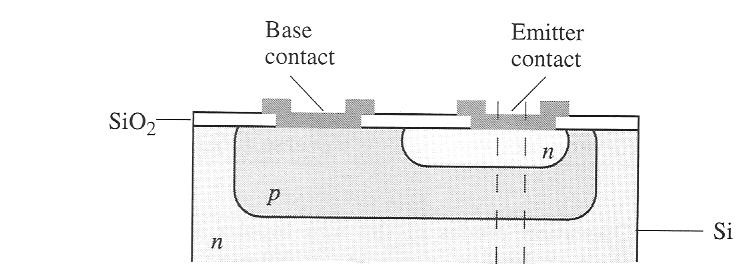
2 Technische Universität Graz Institute of Solid State Physics bipolar transistors npn transistor collector base emitter n+ n p+ p n + lightly doped p substrate Used in front-end high-frequency receivers (mobile telephones), low input impedance amplifier.
3 Ebers-Moll model evbe / kbt / 1 evbc kbt 1 I I e I e E ES R CS evbe / kbt / 1 evbc kbt 1 I I e I e C F ES CS I I I B E C I B I E I RI F F R I C F evbe / kbt evbc / kbt ES 1 IR ICS e 1 I I e

4 Common base configuration evbe / kbt / 1 evbc kbt 1 I I e I e E ES R CS solve for V be I I e I e evbe / kt B / 1 evbc kt B 1 c F ES CS saturation active cutoff I E < 0
5 Common base configuration I c I C ~ I E buffer circuit: the output current is constant over a wide range of output voltages
6 Ebers - Moll Model ea D p ea D n I ES W x W W eabednnb 0 RICS W W be p e0 be n b0 eb e bc be bc be I I F CS ES ea D n W W bc n b0 bc be ea D p ea D n x W W W bc p c0 bc n b0 c c bc be
7 Common emitter configuration evbe / kbt / 1 evbc kbt 1 I I e I e E ES R CS evbe / kbt / 1 evbc kbt 1 I I e I e c F ES CS current amplification ~100 I I I B E C
8 Current amplification factor C fe B I h I B E C I I I 1 1 B C I I 1 1 C e B e I B I B ~ C E I I
9 The Art of Electronics Horowitz and Hill for common emitter configuration
10 Transconductance g m I V C be evbe / kt B / 1 evbc kt B 1 I I e I e c F ES CS The first term depends on V be g m e I ei e I e kt kt kt be B F ES ev / k T C B B B B The transconductance can be very high.
11 Early effect Ebers - Moll: evbe / kbt / 1 evbc kbt 1 I I e I e E ES R CS evbe / kt B / 1 evbc kt B 1 I I e I e c F ES CS I I I B E C I ES ea D p ea D n W x W W be p e0 be n b0 eb e bc be I CS ea D p ea D n x W W W bc p c0 bc n b0 c c bc be I ES and I CS are treated as constants but the depletion widths W bc, W be, W c, and W e depend on the voltages. p ev kt B e0 exp be n ev kt B b0 exp be p ev kt B c0 exp bc n b0 p c0 p exp evbc nb 0 e0 kt B x e W e W eb W x bc W c c

12 Minority carrier concentration n ev kt B b0 exp be p ev kt B e0 exp be n ev kt B b0 exp bc p ev kt B c0 exp bc p c0 p e0 x e x n1 x p1 x p2 x n2 x c
13 Early effect Common emitter configuration Base width modulation: smaller width increases the diffusion current and increases the gain. Punchthrough: The neutral base width goes to zero and all gain is lost. Lightly dope the collector -> voltage drops in collector. Makes circuit slower.

14 I C ~ I B
15 Common emitter configuration I C ~ I B amplifier

16 Small signal response V cc Low input impedance amplifier V transistor V resistor
17 Small signal response i i g v c B EB EB transistor man input conductance: g EB i v B EB transconductance: g m i v c EB
18 Small signal response 1 f 0 1 f ft 0 f
19 Heterojunction bipolar transistors

20 Heterojunction bipolar transistor small emitter-base capacitance to increase speed
21 HBT current gain I C I B 1 n p B0 E0 (npn) Higher doping in the emitter makes the minority carrier concentration lower in the emitter. n B0 p E0 n N 2 i A 2 i n N D N N exp( E / k T) C V gb B NA N N exp( E / k T) C V ge B If the emitter and the base have different band gaps NE NN E c v g exp NB N cn v kbt N D
22 HBT current gain A HBT has an emitter bandgap of 1.62 and a base bandgap of A BJT has an emitter bandgap of 1.42 and a base bandgap of Both have an emitter doping of cm -3 and a base doping of cm -3. How much larger is the gain in the HBT? HBT Eg exp exp 2257 BJT kt B
23 HBT Trade off gain for higher speed Higher base doping lower base resistance reduced Early effect less trouble with punch through base can be made thinner -> faster transistors Because of higher base doping, a higher collector doping is possible without punch through lower collector resistance
24 HBT current gain band discontinuity reduces emitter efficiency Graded layer emitter and base improve performance Si/SiGe AlInAs/InGaAs
25 Heterojunction bipolar transistors Fastest InP/InGaAs HBT's have an f T of 710 GHz. Higher doping in the base allows for a thinner base without punch through and lower base resistance and thus higher frequency operation
26 Microwave engineering Electronics: L<< f <~ 10 GHz Microwave: L 10 GHz < f < 1 THz TeraHertz: L 1 THz < f < 100 THz Optics: L 100 THz
27 Interdigitated contacts in power transistors
28 Thyristors Forward blocking Forward conducting Reverse blocking

29 Thyristors 1 * 2 > 1 Used for switching high currents or voltages


30 Latch-up Both BJT's conduct, creating a low resistance path between V dd and GND. The product of the gains of the two transistors in the feedback loop, is greater than one. The result of latchup is at the minimum a circuit malfunction, and in the worst case, the destruction of the device.

31 Subthreshold current If the p-concentration in the channel is low, electrons emitted into the channel by the forward biased junction diffuse across the channel without recombining.
Institute of Solid State Physics. Technische Universität Graz. Exam. Feb 2, 10:00-11:00 P2
 Technische Universität Graz nstitute of Solid State Physics Exam Feb 2, 10:00-11:00 P2 Exam Four questions, two from the online list. Calculator is ok. No notes. Explain some concept: (tunnel contact,
Memories Bipolar Transistors
 Technische Universität Graz nstitute of Solid State Physics Memories Bipolar Transistors Technische Universität Graz nstitute of Solid State Physics Exams February 5 March 7 April 18 June 27 Exam Four
12. Memories / Bipolar transistors
 Technische Universität Graz Institute of Solid State Physics 12. Memories / Bipolar transistors Jan. 9, 2019 Technische Universität Graz Institute of Solid State Physics Exams January 31 March 8 May 17
EE105 - Fall 2006 Microelectronic Devices and Circuits
 EE105 - Fall 2006 Microelectronic Devices and Circuits Prof. Jan M. Rabaey (jan@eecs) Lecture 21: Bipolar Junction Transistor Administrative Midterm Th 6:30-8pm in Sibley Auditorium Covering everything
ECE-305: Spring 2018 Final Exam Review
 C-305: Spring 2018 Final xam Review Pierret, Semiconductor Device Fundamentals (SDF) Chapters 10 and 11 (pp. 371-385, 389-403) Professor Peter Bermel lectrical and Computer ngineering Purdue University,
Device Physics: The Bipolar Transistor
 Monolithic Amplifier Circuits: Device Physics: The Bipolar Transistor Chapter 4 Jón Tómas Guðmundsson tumi@hi.is 2. Week Fall 2010 1 Introduction In analog design the transistors are not simply switches
UNIVERSITY OF CALIFORNIA, BERKELEY College of Engineering Department of Electrical Engineering and Computer Sciences
 UNIVERSITY OF CALIFORNIA, BERKELEY College of Engineering Department of Electrical Engineering and Computer Sciences EE 105: Microelectronic Devices and Circuits Spring 2008 MIDTERM EXAMINATION #1 Time
Biasing the CE Amplifier
 Biasing the CE Amplifier Graphical approach: plot I C as a function of the DC base-emitter voltage (note: normally plot vs. base current, so we must return to Ebers-Moll): I C I S e V BE V th I S e V th
Lecture 17 - The Bipolar Junction Transistor (I) Forward Active Regime. April 10, 2003
 Forward Active Regime. April 10, 2003") 6.012 - Microelectronic Devices and Circuits - Spring 2003 Lecture 17-1 Lecture 17 - The Bipolar Junction Transistor (I) Contents: Forward Active Regime April 10, 2003 1. BJT: structure and basic operation
6.012 - Microelectronic Devices and Circuits - Spring 2003 Lecture 17-1 Lecture 17 - The Bipolar Junction Transistor (I) Contents: Forward Active Regime April 10, 2003 1. BJT: structure and basic operation
Digital Integrated CircuitDesign
 Digital Integrated CircuitDesign Lecture 5a Bipolar Transistor Dep. Region Neutral Base n(0) b B C n b0 P C0 P e0 P C xn 0 xp 0 x n(w) b W B Adib Abrishamifar EE Department IUST Contents Bipolar Transistor
Metal-oxide-semiconductor field effect transistors (2 lectures)
") Metal-ide-semiconductor field effect transistors ( lectures) MOS physics (brief in book) Current-voltage characteristics - pinch-off / channel length modulation - weak inversion - velocity saturation -
Metal-ide-semiconductor field effect transistors ( lectures) MOS physics (brief in book) Current-voltage characteristics - pinch-off / channel length modulation - weak inversion - velocity saturation -
Lecture 17. The Bipolar Junction Transistor (II) Regimes of Operation. Outline
 Regimes of Operation. Outline") Lecture 17 The Bipolar Junction Transistor (II) Regimes of Operation Outline Regimes of operation Large-signal equivalent circuit model Output characteristics Reading Assignment: Howe and Sodini; Chapter
Lecture 17 The Bipolar Junction Transistor (II) Regimes of Operation Outline Regimes of operation Large-signal equivalent circuit model Output characteristics Reading Assignment: Howe and Sodini; Chapter
Lecture 35 - Bipolar Junction Transistor (cont.) November 27, Current-voltage characteristics of ideal BJT (cont.)
 November 27, Current-voltage characteristics of ideal BJT (cont.)") 6.720J/3.43J - Integrated Microelectronic Devices - Fall 2002 Lecture 35-1 Lecture 35 - Bipolar Junction Transistor (cont.) November 27, 2002 Contents: 1. Current-voltage characteristics of ideal BJT (cont.)
6.720J/3.43J - Integrated Microelectronic Devices - Fall 2002 Lecture 35-1 Lecture 35 - Bipolar Junction Transistor (cont.) November 27, 2002 Contents: 1. Current-voltage characteristics of ideal BJT (cont.)
Bipolar Junction Transistor (BJT) - Introduction
 - Introduction") Bipolar Junction Transistor (BJT) - Introduction It was found in 1948 at the Bell Telephone Laboratories. It is a three terminal device and has three semiconductor regions. It can be used in signal amplification
Bipolar Junction Transistor (BJT) - Introduction It was found in 1948 at the Bell Telephone Laboratories. It is a three terminal device and has three semiconductor regions. It can be used in signal amplification
Electronic Circuits 1. Transistor Devices. Contents BJT and FET Characteristics Operations. Prof. C.K. Tse: Transistor devices
 Electronic Circuits 1 Transistor Devices Contents BJT and FET Characteristics Operations 1 What is a transistor? Three-terminal device whose voltage-current relationship is controlled by a third voltage
Charge-Storage Elements: Base-Charging Capacitance C b
 Charge-Storage Elements: Base-Charging Capacitance C b * Minority electrons are stored in the base -- this charge q NB is a function of the base-emitter voltage * base is still neutral... majority carriers
Spring Semester 2012 Final Exam
 Spring Semester 2012 Final Exam Note: Show your work, underline results, and always show units. Official exam time: 2.0 hours; an extension of at least 1.0 hour will be granted to anyone. Materials parameters
The Devices. Jan M. Rabaey
 The Devices Jan M. Rabaey Goal of this chapter Present intuitive understanding of device operation Introduction of basic device equations Introduction of models for manual analysis Introduction of models
ECE-342 Test 2 Solutions, Nov 4, :00-8:00pm, Closed Book (one page of notes allowed)
") ECE-342 Test 2 Solutions, Nov 4, 2008 6:00-8:00pm, Closed Book (one page of notes allowed) Please use the following physical constants in your calculations: Boltzmann s Constant: Electron Charge: Free
ECE-342 Test 2 Solutions, Nov 4, 2008 6:00-8:00pm, Closed Book (one page of notes allowed) Please use the following physical constants in your calculations: Boltzmann s Constant: Electron Charge: Free
Lecture 17 The Bipolar Junction Transistor (I) Forward Active Regime
 Forward Active Regime") Lecture 17 The Bipolar Junction Transistor (I) Forward Active Regime Outline The Bipolar Junction Transistor (BJT): structure and basic operation I V characteristics in forward active regime Reading Assignment:
Lecture 17 The Bipolar Junction Transistor (I) Forward Active Regime Outline The Bipolar Junction Transistor (BJT): structure and basic operation I V characteristics in forward active regime Reading Assignment:
Final Examination EE 130 December 16, 1997 Time allotted: 180 minutes
 Final Examination EE 130 December 16, 1997 Time allotted: 180 minutes Problem 1: Semiconductor Fundamentals [30 points] A uniformly doped silicon sample of length 100µm and cross-sectional area 100µm 2
Recitation 17: BJT-Basic Operation in FAR
 Recitation 17: BJT-Basic Operation in FAR BJT stands for Bipolar Junction Transistor 1. Can be thought of as two p-n junctions back to back, you can have pnp or npn. In analogy to MOSFET small current
Bipolar junction transistor operation and modeling
 6.01 - Electronic Devices and Circuits Lecture 8 - Bipolar Junction Transistor Basics - Outline Announcements Handout - Lecture Outline and Summary; Old eam 1's on Stellar First Hour Eam - Oct. 8, 7:30-9:30
Mod. Sim. Dyn. Sys. Amplifiers page 1
 AMPLIFIERS A circuit containing only capacitors, amplifiers (transistors) and resistors may resonate. A circuit containing only capacitors and resistors may not. Why does amplification permit resonance
Forward-Active Terminal Currents
 Forward-Active Terminal Currents Collector current: (electron diffusion current density) x (emitter area) diff J n AE qd n n po A E V E V th ------------------------------ e W (why minus sign? is by def.
ELEC 3908, Physical Electronics, Lecture 17. Bipolar Transistor Injection Models
 LC 3908, Physical lectronics, Lecture 17 Bipolar Transistor njection Models Lecture Outline Last lecture looked at qualitative operation of the BJT, now want to develop a quantitative model to predict
Mod. Sim. Dyn. Sys. Amplifiers page 1
 AMPLIFIERS A circuit containing only capacitors, amplifiers (transistors) and resistors may resonate. A circuit containing only capacitors and resistors may not. Why does amplification permit resonance
R. Ludwig and G. Bogdanov RF Circuit Design: Theory and Applications 2 nd edition. Figures for Chapter 6
 R. Ludwig and G. Bogdanov RF Circuit Design: Theory and Applications 2 nd edition Figures for Chapter 6 Free electron Conduction band Hole W g W C Forbidden Band or Bandgap W V Electron energy Hole Valence
The Devices: MOS Transistors
 The Devices: MOS Transistors References: Semiconductor Device Fundamentals, R. F. Pierret, Addison-Wesley Digital Integrated Circuits: A Design Perspective, J. Rabaey et.al. Prentice Hall NMOS Transistor
6.012 Electronic Devices and Circuits
 Page 1 of 12 YOUR NAME Department of Electrical Engineering and Computer Science Massachusetts Institute of Technology 6.012 Electronic Devices and Circuits FINAL EXAMINATION Open book. Notes: 1. Unless
Introduction to Transistors. Semiconductors Diodes Transistors
 Introduction to Transistors Semiconductors Diodes Transistors 1 Semiconductors Typical semiconductors, like silicon and germanium, have four valence electrons which form atomic bonds with neighboring atoms
Chapter 2. - DC Biasing - BJTs
 Chapter 2. - DC Biasing - BJTs Objectives To Understand : Concept of Operating point and stability Analyzing Various biasing circuits and their comparison with respect to stability BJT A Review Invented
EE 230 Lecture 31. THE MOS TRANSISTOR Model Simplifcations THE Bipolar Junction TRANSISTOR
 EE 23 Lecture 3 THE MOS TRANSISTOR Model Simplifcations THE Bipolar Junction TRANSISTOR Quiz 3 Determine I X. Assume W=u, L=2u, V T =V, uc OX = - 4 A/V 2, λ= And the number is? 3 8 5 2? 6 4 9 7 Quiz 3
ELECTRONICS IA 2017 SCHEME
 ELECTRONICS IA 2017 SCHEME CONTENTS 1 [ 5 marks ]...4 2...5 a. [ 2 marks ]...5 b. [ 2 marks ]...5 c. [ 5 marks ]...5 d. [ 2 marks ]...5 3...6 a. [ 3 marks ]...6 b. [ 3 marks ]...6 4 [ 7 marks ]...7 5...8
ECE 497 JS Lecture - 12 Device Technologies
 ECE 497 JS Lecture - 12 Device Technologies Spring 2004 Jose E. Schutt-Aine Electrical & Computer Engineering University of Illinois jose@emlab.uiuc.edu 1 NMOS Transistor 2 ρ Source channel charge density
Semiconductor Physics fall 2012 problems
 Semiconductor Physics fall 2012 problems 1. An n-type sample of silicon has a uniform density N D = 10 16 atoms cm -3 of arsenic, and a p-type silicon sample has N A = 10 15 atoms cm -3 of boron. For each
Erik Lind
 High-Speed Devices, 2011 Erik Lind (Erik.Lind@ftf.lth.se) Course consists of: 30 h Lectures (H322, and Fys B check schedule) 8h Excercises 2x2h+4h Lab Excercises (2 Computer simulations, 4 RF measurment
ELEC 3908, Physical Electronics, Lecture 19. BJT Base Resistance and Small Signal Modelling
 ELEC 3908, Physical Electronics, Lecture 19 BJT Base Resistance and Small Signal Modelling Lecture Outline Lecture 17 derived static (dc) injection model to predict dc currents from terminal voltages This
9. Semiconductor Devices /Phonons
 Technische Universität Graz Institute of Solid State Physics 9. Semiconductor Devices /Phonons Oct 29, 2018 p and n profiles p n V bi ~ 1 V E c W ~ 1 m E F E max ~ 10 4 V/cm ev bi E v p Ev E F Nv exp kt
Lecture 23: Negative Resistance Osc, Differential Osc, and VCOs
 EECS 142 Lecture 23: Negative Resistance Osc, Differential Osc, and VCOs Prof. Ali M. Niknejad University of California, Berkeley Copyright c 2005 by Ali M. Niknejad A. M. Niknejad University of California,
Chapter 2 - DC Biasing - BJTs
 Objectives Chapter 2 - DC Biasing - BJTs To Understand: Concept of Operating point and stability Analyzing Various biasing circuits and their comparison with respect to stability BJT A Review Invented
BJT - Mode of Operations
 JT - Mode of Operations JTs can be modeled by two back-to-back diodes. N+ P N- N+ JTs are operated in four modes. HO #6: LN 251 - JT M Models Page 1 1) Forward active / normal junction forward biased junction
figure shows a pnp transistor biased to operate in the active mode
 Lecture 10b EE-215 Electronic Devices and Circuits Asst Prof Muhammad Anis Chaudhary BJT: Device Structure and Physical Operation The pnp Transistor figure shows a pnp transistor biased to operate in the
ECE 305 Fall Final Exam (Exam 5) Wednesday, December 13, 2017
 Wednesday, December 13, 2017") NAME: PUID: ECE 305 Fall 017 Final Exam (Exam 5) Wednesday, December 13, 017 This is a closed book exam. You may use a calculator and the formula sheet at the end of this exam. Following the ECE policy,
NAME: PUID: ECE 305 Fall 017 Final Exam (Exam 5) Wednesday, December 13, 017 This is a closed book exam. You may use a calculator and the formula sheet at the end of this exam. Following the ECE policy,
Semiconductor Physics Problems 2015
 Semiconductor Physics Problems 2015 Page and figure numbers refer to Semiconductor Devices Physics and Technology, 3rd edition, by SM Sze and M-K Lee 1. The purest semiconductor crystals it is possible
8. Schottky contacts / JFETs
 Technische Universität Graz Institute of Solid State Physics 8. Schottky contacts / JFETs Nov. 21, 2018 Technische Universität Graz Institute of Solid State Physics metal - semiconductor contacts Photoelectric
Chapter 13 Small-Signal Modeling and Linear Amplification
 Chapter 13 Small-Signal Modeling and Linear Amplification Microelectronic Circuit Design Richard C. Jaeger Travis N. Blalock 1/4/12 Chap 13-1 Chapter Goals Understanding of concepts related to: Transistors
Whereas the diode was a 1-junction device, the transistor contains two junctions. This leads to two possibilities:
 Part Recall: two types of charge carriers in semiconductors: electrons & holes two types of doped semiconductors: n-type (favor e-), p-type (favor holes) for conduction Whereas the diode was a -junction
EE 466/586 VLSI Design. Partha Pande School of EECS Washington State University
 EE 466/586 VLSI Design Partha Pande School of EECS Washington State University pande@eecs.wsu.edu Lecture 8 Power Dissipation in CMOS Gates Power in CMOS gates Dynamic Power Capacitance switching Crowbar
CHAPTER 4: P-N P N JUNCTION Part 2. M.N.A. Halif & S.N. Sabki
 CHAPTER 4: P-N P N JUNCTION Part 2 Part 2 Charge Storage & Transient Behavior Junction Breakdown Heterojunction CHARGE STORAGE & TRANSIENT BEHAVIOR Once injected across the junction, the minority carriers
Schottky diodes. JFETs - MESFETs - MODFETs
 Technische Universität Graz Institute of Solid State Physics Schottky diodes JFETs - MESFETs - MODFETs Quasi Fermi level When the charge carriers are not in equilibrium the Fermi energy can be different
ELEC 3908, Physical Electronics, Lecture 18. The Early Effect, Breakdown and Self-Heating
 ELEC 3908, Physical Electronics, Lecture 18 The Early Effect, Breakdown and Self-Heating Lecture Outline Previous 2 lectures analyzed fundamental static (dc) carrier transport in the bipolar transistor
Introduction to Power Semiconductor Devices
 ECE442 Power Semiconductor Devices and Integrated Circuits Introduction to Power Semiconductor Devices Zheng Yang (ERF 3017, email: yangzhen@uic.edu) Power Semiconductor Devices Applications System Ratings
Electronic Circuits Summary
 Electronic Circuits Summary Andreas Biri, D-ITET 6.06.4 Constants (@300K) ε 0 = 8.854 0 F m m 0 = 9. 0 3 kg k =.38 0 3 J K = 8.67 0 5 ev/k kt q = 0.059 V, q kt = 38.6, kt = 5.9 mev V Small Signal Equivalent
(e V BC/V T. α F I SE = α R I SC = I S (3)
") Experiment #8 BJT witching Characteristics Introduction pring 2015 Be sure to print a copy of Experiment #8 and bring it with you to lab. There will not be any experiment copies available in the lab. Also
Experiment #8 BJT witching Characteristics Introduction pring 2015 Be sure to print a copy of Experiment #8 and bring it with you to lab. There will not be any experiment copies available in the lab. Also
Current mechanisms Exam January 27, 2012
 Current mechanisms Exam January 27, 2012 There are four mechanisms that typically cause currents to flow: thermionic emission, diffusion, drift, and tunneling. Explain briefly which kind of current mechanisms
Chapter 2 CMOS Transistor Theory. Jin-Fu Li Department of Electrical Engineering National Central University Jungli, Taiwan
 Chapter 2 CMOS Transistor Theory Jin-Fu Li Department of Electrical Engineering National Central University Jungli, Taiwan Outline Introduction MOS Device Design Equation Pass Transistor Jin-Fu Li, EE,
Lecture 19 - p-n Junction (cont.) October 18, Ideal p-n junction out of equilibrium (cont.) 2. pn junction diode: parasitics, dynamics
 October 18, Ideal p-n junction out of equilibrium (cont.) 2. pn junction diode: parasitics, dynamics") 6.720J/3.43J - Integrated Microelectronic Devices - Fall 2002 Lecture 19-1 Lecture 19 - p-n Junction (cont.) October 18, 2002 Contents: 1. Ideal p-n junction out of equilibrium (cont.) 2. pn junction diode:
6.720J/3.43J - Integrated Microelectronic Devices - Fall 2002 Lecture 19-1 Lecture 19 - p-n Junction (cont.) October 18, 2002 Contents: 1. Ideal p-n junction out of equilibrium (cont.) 2. pn junction diode:
EE 3329 Electronic Devices Syllabus ( Extended Play )
") EE 3329 - Electronic Devices Syllabus EE 3329 Electronic Devices Syllabus ( Extended Play ) The University of Texas at El Paso The following concepts can be part of the syllabus for the Electronic Devices
EE 3329 - Electronic Devices Syllabus EE 3329 Electronic Devices Syllabus ( Extended Play ) The University of Texas at El Paso The following concepts can be part of the syllabus for the Electronic Devices
About Modeling the Reverse Early Effect in HICUM Level 0
 About Modeling the Reverse Early Effect in HICUM Level 0 6 th European HICUM Workshop, June 12-13, 2006, Heilbronn Didier CELI, STMicroelectronics 1/21 D. Céli Purpose According to the bipolar models,
Session 6: Solid State Physics. Diode
 Session 6: Solid State Physics Diode 1 Outline A B C D E F G H I J 2 Definitions / Assumptions Homojunction: the junction is between two regions of the same material Heterojunction: the junction is between
For the following statements, mark ( ) for true statement and (X) for wrong statement and correct it.
 for true statement and (X) for wrong statement and correct it.") Benha University Faculty of Engineering Shoubra Electrical Engineering Department First Year communications. Answer all the following questions Illustrate your answers with sketches when necessary. The
Benha University Faculty of Engineering Shoubra Electrical Engineering Department First Year communications. Answer all the following questions Illustrate your answers with sketches when necessary. The
and V DS V GS V T (the saturation region) I DS = k 2 (V GS V T )2 (1+ V DS )
 I DS = k 2 (V GS V T )2 (1+ V DS )") ECE 4420 Spring 2005 Page 1 FINAL EXAMINATION NAME SCORE /100 Problem 1O 2 3 4 5 6 7 Sum Points INSTRUCTIONS: This exam is closed book. You are permitted four sheets of notes (three of which are your sheets
ECE 4420 Spring 2005 Page 1 FINAL EXAMINATION NAME SCORE /100 Problem 1O 2 3 4 5 6 7 Sum Points INSTRUCTIONS: This exam is closed book. You are permitted four sheets of notes (three of which are your sheets
CLASS 3&4. BJT currents, parameters and circuit configurations
 CLASS 3&4 BJT currents, parameters and circuit configurations I E =I Ep +I En I C =I Cp +I Cn I B =I BB +I En -I Cn I BB =I Ep -I Cp I E = I B + I C I En = current produced by the electrons injected from
Student Number: CARLETON UNIVERSITY SELECTED FINAL EXAMINATION QUESTIONS
 Name: CARLETON UNIVERSITY SELECTE FINAL EXAMINATION QUESTIONS URATION: 6 HOURS epartment Name & Course Number: ELEC 3908 Course Instructors: S. P. McGarry Authorized Memoranda: Non-programmable calculators
Avalanche breakdown. Impact ionization causes an avalanche of current. Occurs at low doping
 Avalanche breakdown Impact ionization causes an avalanche of current Occurs at low doping Zener tunneling Electrons tunnel from valence band to conduction band Occurs at high doping Tunneling wave decays
Physics of Semiconductors 8 th
 Physics of Semiconductors 8 th 2016.6.6 Shingo Katsumoto Department of Physics, Institute for Solid State Physics University of Tokyo Review of pn junction Estimation of builtin potential Depletion layer
Vidyalankar S.E. Sem. III [EXTC] Analog Electronics - I Prelim Question Paper Solution
![Vidyalankar S.E. Sem. III [EXTC] Analog Electronics - I Prelim Question Paper Solution](/thumbs/90/101612294.jpg "Vidyalankar S.E. Sem. III [EXTC] Analog Electronics - I Prelim Question Paper Solution") . (a) S.E. Sem. [EXTC] Analog Electronics - Prelim Question Paper Solution Comparison between BJT and JFET BJT JFET ) BJT is a bipolar device, both majority JFET is an unipolar device, electron and minority
. (a) S.E. Sem. [EXTC] Analog Electronics - Prelim Question Paper Solution Comparison between BJT and JFET BJT JFET ) BJT is a bipolar device, both majority JFET is an unipolar device, electron and minority
Junction Bipolar Transistor. Characteristics Models Datasheet
 Junction Bipolar Transistor Characteristics Models Datasheet Characteristics (1) The BJT is a threeterminal device, terminals are named emitter, base and collector. Small signals, applied to the base,
6.012 Electronic Devices and Circuits
 Page 1 of 1 YOUR NAME Department of Electrical Engineering and Computer Science Massachusetts Institute of Technology 6.12 Electronic Devices and Circuits Exam No. 1 Wednesday, October 7, 29 7:3 to 9:3
Plan Bipolar junction transistor Elements of small-signal analysis Transistor Principles: PETs and FETs Field effect transistor Discussion
 Physics of silicon transistors - 1 - Plan Bipolar junction transistor homojunction and heterojunction Doping considerations Transport factor and current gain Frequency dependence of gain in a microwave
Switching circuits: basics and switching speed
 ECE137B notes; copyright 2018 Switching circuits: basics and switching speed Mark Rodwell, University of California, Santa Barbara Amplifiers vs. switching circuits Some transistor circuit might have V
CHAPTER.4: Transistor at low frequencies
 CHAPTER.4: Transistor at low frequencies Introduction Amplification in the AC domain BJT transistor modeling The re Transistor Model The Hybrid equivalent Model Introduction There are three models commonly
6.012 Electronic Devices and Circuits Spring 2005
 6.012 Electronic Devices and Circuits Spring 2005 May 16, 2005 Final Exam (200 points) -OPEN BOOK- Problem NAME RECITATION TIME 1 2 3 4 5 Total General guidelines (please read carefully before starting):
EE 230 Lecture 33. Nonlinear Circuits and Nonlinear Devices. Diode BJT MOSFET
 EE 230 Lecture 33 Nonlinear Circuits and Nonlinear Devices Diode BJT MOSFET Review from Last Time: n-channel MOSFET Source Gate L Drain W L EFF Poly Gate oxide n-active p-sub depletion region (electrically
Capacitors Diodes Transistors. PC200 Lectures. Terry Sturtevant. Wilfrid Laurier University. June 4, 2009
 Wilfrid Laurier University June 4, 2009 Capacitor an electronic device which consists of two conductive plates separated by an insulator Capacitor an electronic device which consists of two conductive
Electronic Circuits. Bipolar Junction Transistors. Manar Mohaisen Office: F208 Department of EECE
 Electronic Circuits Bipolar Junction Transistors Manar Mohaisen Office: F208 Email: manar.subhi@kut.ac.kr Department of EECE Review of Precedent Class Explain the Operation of the Zener Diode Explain Applications
ID # NAME. EE-255 EXAM 3 April 7, Instructor (circle one) Ogborn Lundstrom
 Ogborn Lundstrom") ID # NAME EE-255 EXAM 3 April 7, 1998 Instructor (circle one) Ogborn Lundstrom This exam consists of 20 multiple choice questions. Record all answers on this page, but you must turn in the entire exam.
ID # NAME EE-255 EXAM 3 April 7, 1998 Instructor (circle one) Ogborn Lundstrom This exam consists of 20 multiple choice questions. Record all answers on this page, but you must turn in the entire exam.
junctions produce nonlinear current voltage characteristics which can be exploited
 Chapter 6 P-N DODES Junctions between n-and p-type semiconductors are extremely important foravariety of devices. Diodes based on p-n junctions produce nonlinear current voltage characteristics which can
Decemb er 20, Final Exam
 Fall 2002 6.720J/3.43J Integrated Microelectronic Devices Prof. J. A. del Alamo Decemb er 20, 2002 - Final Exam Name: General guidelines (please read carefully b efore starting): Make sure to write your
BJT Biasing Cont. & Small Signal Model
 BJT Biasing Cont. & Small Signal Model Conservative Bias Design (1/3, 1/3, 1/3 Rule) Bias Design Example Small-Signal BJT Models Small-Signal Analysis 1 Emitter Feedback Bias Design R B R C V CC R 1 R
Figure 1 Basic epitaxial planar structure of NPN. Figure 2 The 3 regions of NPN (left) and PNP (right) type of transistors
 and PNP (right) type of transistors") Figure 1 Basic epitaxial planar structure of NPN Figure 2 The 3 regions of NPN (left) and PNP (right) type of transistors Lecture Notes: 2304154 Physics and Electronics Lecture 6 (2 nd Half), Year: 2007
Figure 1 Basic epitaxial planar structure of NPN Figure 2 The 3 regions of NPN (left) and PNP (right) type of transistors Lecture Notes: 2304154 Physics and Electronics Lecture 6 (2 nd Half), Year: 2007
p-n junction biasing, p-n I-V characteristics, p-n currents Norlaili Mohd. Noh EEE /09
 CLASS 6&7 p-n junction biasing, p-n I-V characteristics, p-n currents 1 p-n junction biasing Unbiased p-n junction: the potential barrier is 0.7 V for Si and 0.3 V for Ge. Nett current across the p-n junction
2. Crystals and Current Carriers
 miconductor Devices Summary Andreas Biri, D-ITET 30.07.4. Constants & Various Constants (@300K) 8.854 0 9. 0.38 0 8.67 0 / 0.0259, 38.6, 25.9.602 0 #.602 0 # $ % Silicon (@300K) -> 4 valence electrons
The Devices. Devices
 The The MOS Transistor Gate Oxyde Gate Source n+ Polysilicon Drain n+ Field-Oxyde (SiO 2 ) p-substrate p+ stopper Bulk Contact CROSS-SECTION of NMOS Transistor Cross-Section of CMOS Technology MOS transistors
Charge-storage related parameter calculation for Si and SiGe bipolar transistors from device simulation
 Charge-storage related parameter calculation for Si and SiGe bipolar transistors from device simulation M. Schroter ),) and H. Tran ) ) ECE Dept., University of California San Diego, La Jolla, CA, USA
SOME USEFUL NETWORK THEOREMS
 APPENDIX D SOME USEFUL NETWORK THEOREMS Introduction In this appendix we review three network theorems that are useful in simplifying the analysis of electronic circuits: Thévenin s theorem Norton s theorem
Fundamentals of Semiconductor Physics
 Fall 2007 Fundamentals of Semiconductor Physics 万 歆 Zhejiang Institute of Modern Physics xinwan@zimp.zju.edu.cn http://zimp.zju.edu.cn/~xinwan/ Transistor technology evokes new physics The objective of
Transistor Characteristics and A simple BJT Current Mirror
 Transistor Characteristics and A simple BJT Current Mirror Current-oltage (I-) Characteristics Device Under Test DUT i v T T 1 R X R X T for test Independent variable on horizontal axis Could force current
Problem 9.20 Threshold bias for an n-channel MOSFET: In the text we used a criterion that the inversion of the MOSFET channel occurs when V s = ;2 F w
 Prof. Jasprit Singh Fall 2001 EECS 320 Homework 11 The nals for this course are set for Friday December 14, 6:30 8:30 pm and Friday Dec. 21, 10:30 am 12:30 pm. Please choose one of these times and inform
Lecture 15: MOS Transistor models: Body effects, SPICE models. Context. In the last lecture, we discussed the modes of operation of a MOS FET:
 Lecture 15: MOS Transistor models: Body effects, SPICE models Context In the last lecture, we discussed the modes of operation of a MOS FET: oltage controlled resistor model I- curve (Square-Law Model)
Devices. chapter Introduction. 1.2 Silicon Conductivity
 chapter 1 Devices 1.1 Introduction The properties and performance of analog bicmos integrated circuits are dependent on the devices used to construct them. This chapter is a review of the operation of
Circle the one best answer for each question. Five points per question.
 ID # NAME EE-255 EXAM 3 November 8, 2001 Instructor (circle one) Talavage Gray This exam consists of 16 multiple choice questions and one workout problem. Record all answers to the multiple choice questions
GATE SOLVED PAPER - EC
 03 ONE MARK Q. In a forward biased pn junction diode, the sequence of events that best describes the mechanism of current flow is (A) injection, and subsequent diffusion and recombination of minority carriers
The Devices. Digital Integrated Circuits A Design Perspective. Jan M. Rabaey Anantha Chandrakasan Borivoje Nikolic. July 30, 2002
 Digital Integrated Circuits A Design Perspective Jan M. Rabaey Anantha Chandrakasan Borivoje Nikolic The Devices July 30, 2002 Goal of this chapter Present intuitive understanding of device operation Introduction
CMOS Devices. PN junctions and diodes NMOS and PMOS transistors Resistors Capacitors Inductors Bipolar transistors
 CMOS Devices PN junctions and diodes NMOS and PMOS transistors Resistors Capacitors Inductors Bipolar transistors PN Junctions Diffusion causes depletion region D.R. is insulator and establishes barrier
Trench IGBT failure mechanisms evolution with temperature and gate resistance under various short-circuit conditions
 Author manuscript, published in "Microelectronics Reliability vol.47 (7) pp.173-1734" Trench IGBT failure mechanisms evolution with temperature and gate resistance under various short-circuit conditions
Lecture 16 - The pn Junction Diode (II) Equivalent Circuit Model. April 8, 2003
 Equivalent Circuit Model. April 8, 2003") 6.012 - Microelectronic Devices and Circuits - Spring 2003 Lecture 16-1 Lecture 16 - The pn Junction Diode (II) Equivalent Circuit Model April 8, 2003 Contents: 1. I-V characteristics (cont.) 2. Small-signal
6.012 - Microelectronic Devices and Circuits - Spring 2003 Lecture 16-1 Lecture 16 - The pn Junction Diode (II) Equivalent Circuit Model April 8, 2003 Contents: 1. I-V characteristics (cont.) 2. Small-signal
Appendix 1: List of symbols
 Appendix 1: List of symbols Symbol Description MKS Units a Acceleration m/s 2 a 0 Bohr radius m A Area m 2 A* Richardson constant m/s A C Collector area m 2 A E Emitter area m 2 b Bimolecular recombination
MSE 310/ECE 340: Electrical Properties of Materials Fall 2014 Department of Materials Science and Engineering Boise State University
 MSE 310/ECE 340: Electrical Properties of Materials Fall 2014 Department of Materials Science and Engineering Boise State University Practice Final Exam 1 Read the questions carefully Label all figures