Supplementary Reader. EECS 40 Introduction to Microelectronic Circuits
|
|
|
- Abigail Johns
- 5 years ago
- Views:
Transcription
1 Supplementary eader EECS 4 Introduction to Microelectronic Circuits Prof. C. Chang-Hasnain Spring 7 Note: This set of notes is intended to supplement the text book and not to replace it.
2 EE 4, University of California Berkeley Professor Chang-Hasnain Table of Contents Table of Contents... i Chapter. Bode Plots.... Introduction.... First Order Circuits..... General Construction and Break Frequency..... Bode Magnitude Plot Bode Phase Plot Second Order Circuits General Construction and esonant Frequency Bode Magnitude Plot Bode Phase Plot Definitions... Chapter. Diode Circuits Physical Behavior of Diodes Solving Diode Circuits Proof by Contradiction Approach Load Line Analysis Zener Diodes Applications for Diodes Clipper Circuit (a.k.a. Limiter Circuit) Level Shift Circuit Clamping Circuit (a.k.a. DC estorer) ectifier Circuit Peak Detector oltage Doubler Circuit Diode Logic Gates... 6 Chapter 3. Semiconductor Physics Introduction to Silicon Bandgap Energy Fermi Energy Doping Doping Methods Quantitative Analysis Electric Fields Electrostatic Potential i
3 EE 4, University of California Berkeley Professor Chang-Hasnain 3.3 PN Junction Depletion Approximation PN Junction in Equilibrium everse Bias Forward Bias eferences... 4 Chapter 4. Metal-Oxide-Semiconductor Field-Effect Transistor (MOSFET) Introduction Notation NMOS and PMOS Transistors N-MOSFET Operating egions Cut-off Triode Saturation PMOSFET Operating egions Chapter 5. Simple MOSFET Circuits Analysis for MOSFET Amplifiers DC Analysis Load-Line Analysis Small-Signal Equivalent Circuit Finding oltage Gains, Input, and Output esistances The Inverter: Constructing a Logic Gate: the Use of Pull-Down and Pull-Up Networks NMOS esistor Pull-Up The CMOS Inverter Input NAND Gate: Input NO Gate Past Exams Acknowledgements We thank Abhinav Gupta, Kevin Wang, Henry Wang, and Wendy Xiao-Xue Zhao for the assistance in preparing this manuscript, and detailed editing by Isaac Seetho, Yu Ben, Timothy C Loo, Jia Zou, and Michael Krishnan. ii
4 EE 4, University of California Berkeley Prof. Chang-Hasnain. Introduction Chapter. Bode Plots Bode plots are widely used in various fields of engineering because they characterize the magnitude and the phase response of a system. In this section, we will present step-by-step analysis to create the Bode plots of a given transfer function. We analyze the trend of the transfer function at different frequency regimes based on the value of the break or resonant frequency. This approach helps to understand the frequency behavior of the circuit, and also works for first order, second and higher order circuits.. First Order Circuits.. General Construction and Break Frequency A Bode plot illustrates the behavior of a circuit by generalizing its response into trends and graphing it against a log scale of frequency. Given a transfer function, H(), we may produce a magnitude and phase Bode plot. In each plot, we break down the analysis of the transfer function into 3 regimes, depending on the frequency in question:. At ω= ωb,. when 3. when ω<< ω B, or when ω is much less than the break frequency ω>> ω B, or when ω is much greater than the break frequency The break frequency, ω, is a property of the filter that can be found by examining the transfer function. It B describes the frequency where the trends on the Bode plot are broken, where one trend (when ends and the next (when ω>> ω B ) begins. ω<< ) For first-order circuits, the break frequency can be found by looking solving for the frequency at which the real and complex components are equal. ω B Example Find the Break Frequency Given the transfer function H ( ω) =. We find the break frequency by examining the jωc denominator, because it consists of two terms, and jω C. The first term is real and has a dependence. The second term jω C has a ω dependence. The break frequency, ω B, occurs when the MAGNITUDE two components are equal. Thus, the break frequency for a filter with this transfer function is at ω B =. C After finding the break frequency, we can examine the trends on either side of ω B. When ω << ω B, the real term (in the denominator of Exp. ) dominates and we ignore the imaginary component. When ω >>, ω dominates real term, so we work with only the imaginary term, as will be shown next. ω B Note: We can only disregard terms that are added and subtracted and not those that are multiplied or divided when making approximations. ω - -
5 EE 4, University of California Berkeley Professor Chang-Hasnain e.g For a<<b, a<c and c<<d, ( c d) a b ad b Try to plug in any number you like and see if it is true... Bode Magnitude Plot For the magnitude plot, we plot on the y-axis: the square of the magnitude of the transfer function, H (ω) in decibels (unit db). This is because the transfer function describes the output to input voltage ratio. Since power is proportional to, we plot H (ω), which in db is: H ( ω) db = log H ( ω) = log H ( ω) () Both of these expressions can be useful, depending on the form of the transfer function. H ) db We plot (ω on the y-axis, against a logarithmic scale of ω on the x-axis. One thing to keep in mind about logarithmic functions is the ability to pull multiplicative factors out, for instance: The key to our analysis is that we identify and examine the dominant terms of the transfer function in each of the 3 regimes in the following. () At ω = ω B, we simply plugω B in H (ω) and get the actual value. db () When ω<< ω B. Examine SEPEATELY in the numerator and denominator all terms containing ω (e.g. ω, ω ). The one with the lowest power (e.g. ω ) dominates in this frequency range. Hence we keep only the dominating term, one each for the numerator and denominator, respectively. The resulting formula will be used to determine the asymptotic behavior, or trend. (3) When ω>> ω B. Again, we examine the numerator and denominator separately. Leave only the term with the highest power (ω in the previous example), one each for numerator and dominator. The resulting formula will be used to determine the asymptotic behavior, or trend. By analyzing these three regimes, we can construct the magnitude Bode plot. We start at the break frequency, ω = ω, and then plot the trends for ω<< and ω>>. B log( A B) = log A log B C log( ) = logc log D D Example Find the Transfer Function, H (ω), and plot the magnitude Bode Plot. ω B Given the following circuit, construct the magnitude Bode plot. in T A T C out ω B A = = Ω = kω C = µ F
6 EE 4, University of California Berkeley Professor Chang-Hasnain We can see where T = Z c = j ω C Thus, the transfer function is given by: in By voltage divider, we have: out Zc = Z c A out Z c H ( ω) = = A in Z c / jωc = A = / jωc in A jω C The magnitude plot will be the transfer function in db, or: H ( ω) db = log H ( ω) A = log jω C Plotting this function would yield the exact behavior of our filter, but we only need the asymptotic behavior for the Bode plot. Now we begin a 3-part analysis. Step : Break Frequency Setting equal the real and imaginary components in the denominator, we find the break frequency: ω B = = C (k)( F) rad = = rad/s s Step : Asymptotes () At ω = ωb, With A =, H( ω B ) = 37 db. The first line of the above steps shows that at ω db B, the output is at half the maximum power (-3dB is half in linear scale); the transfer function (voltage) has a value of A, and power is proportional to the square of voltage. The break frequency for a first-order circuit is also referred to as the half-power frequency, where the output is one-half the maximum power. The factor of / in the logarithm can be expanded out to - log : The half-power frequency is -3dB below the maximum power, so we also call ω<< ω H ( ω ) B db A A A = log = log = log j = log A log = log A 3dB log = log log = log 3 db ω B the -3dB frequency. () For B, the constant dominates in the denominator and is the only term to be kept.. The transfer function can be approximated as: A H (ω) = A 3
 Next, forω>> ωb, the ω term dominates in the denominator term, and the transfer function can be approximated as: A H ( ω) jω C A A H ( ω) = log = log log jω db jωc C A ' = log logω = C logω C In")
7 EE 4, University of California Berkeley Professor Chang-Hasnain which is purely real, so H( ω ) = log A and db Substituting the gain factor, A =, we obtain H( ω) = log = = 4 db. (3) Next, forω>> ωb, the ω term dominates in the denominator term, and the transfer function can be approximated as: A H ( ω) jω C A A H ( ω) = log = log log jω db jωc C A ' = log logω = C logω C In the asymptote, the filter s magnitude decreases at a rate of db/decade (a x increase inω ). Here C is a constant and we can simply connect the curve for ω>> ω with the point H( ω ) = 37 db. The magnitude H (ω B ) decreases by db at ω B, 4 db at ω B, and so on. db H (ω) = A = A With these three regions analyzed, the magnitude Bode plot is complete and shown in Fig.. db B B db ( B ) Fig.. Magnitude Bode Plot for H() of Example, with the gain factor A =. The dotted straight lines in Fig.. form the Bode plot. Note how it approximates the behavior of the actual function, shown in blue. NOTE: This is an example of low-pass filter. The low frequencies are kept by the filter and the high frequencies are filtered out. First-order circuits are either high-pass or low-pass filters. Exercise : What if the voltage across the resistor (Example ) is taken as the output? Is the total energy conserved in each frequency? 4
8 EE 4, University of California Berkeley Professor Chang-Hasnain..3 Bode Phase Plot The Bode phase plot is constructed in a similar manner to the magnitude plot except we use limits (instead of trends). We first find the expression for phase, H (ω), from the transfer function, H (ω). For ω<< ω B, we take the limit of H (ω) as ω. At ω = ωb, we use the complete expression for H (ω), as both the real and imaginary components have equal magnitude. For ω>> ωb, we find the phase by taking the limit of H (ω) as ω. We then construct the Bode phase plot by performing the following: Plot lower-frequency limit value (from x ω<< ωb to B /), Plot upper-frequency limit value (from x= B to ω ) Plot the value for ω = ωb Connect the extremes by curve (arctan) lines. Example 3 Find the Phase,, of a Transfer Function, H (ω) Using the transfer function of Example, H ( ω) = A jω C We find the net phase, H (ω), by subtracting the phase of the denominator from the phase of the numerator: ωc H ( ω) = tan = tan ω C To plot the expression for phase in Exp. 3, we examine our 3 regions. Taking the limit of H (ω) as ω, we find the lower-frequency asymptote, ω<< ωb. The upper-frequency asymptote, ω>> ω is found by taking the limit as ω : lim H ( ω) = tan ω B ( ) ( ) = H ( ω B ) = tan = 45 or 4 This value is in agreement with a line drawn between the upper and lower asymptotes; ωb is halfway between ωb and ω, and -45 is halfway in between and 9. The phase Bode plot of Exp. 3 is B shown in Fig.. ( ) lim H ( ω) = tan = 9 or ω At the break frequency, ω B =, we find the phase to be: C π ( ) π 5

9 EE 4, University of California Berkeley Professor Chang-Hasnain Fig ( B ) ( B /) ( B ) Fig.. Phase Bode Plot for H() of Example. As before, the dotted lines in Fig. outline the phase Bode plot for our transfer function, but the actual values are shown by the solid line. Note that with our approximation, in the intermediate region between B / and B, the phase decreases by 45 degrees per decade of angular frequency, and outside this region, the phase is constant (the asymptote). Exercise : Find the Transfer Function, H (ω), and plot Bode magnitude and phase plots for (a) out = L and (b) out =. In both cases, do we have high-pass or low-pass filters? v - in - L v L - 6
10 EE 4, University of California Berkeley Professor Chang-Hasnain.3 Second Order Circuits.3. General Construction and esonant Frequency As with Bode Plots for first-order circuits, the transfer function for second-order circuits can be found by writing an equation relating out and in. Once this equation is written, an expression for H (ω) is easily obtained. You can use this transfer function to find its magnitude and phase. Similar to first-order circuits, we depict the behavior of second-order circuits by plotting trends of the transfer function at three frequency regimes relative to a certain resonance frequency, ω :. At ω= ωo. For ωo ω<<, or in other words, the limit as ω 3. For ω>> ωo, or in the limit as ω Around the resonant frequency, the magnitude of the transfer function H (ω) changes trend and often reaches the maximum or minimum value. Though whether it reaches the maximum or minimum depends greatly on the Q value, which will be discussed next, the trend is always changed at the resonance frequency. The resonant frequency, ω, can be found by setting the complex part of either numerator or denominator of the transfer function to zero. This is because the magnitude of a jb reaches minimum when b=. If we have a complex term a jb on the numerator, by letting b=, we reached minimum, whereas if this complex term is in the denominator, we reached maximum. Example 4: Finding the resonant frequency For a circuit with transfer function as H ( ω) = jωl j ωc What isω, the resonant frequency? Solution: o The numerator is, which has no frequency dependence term and hence irrelevant for this question. We look at the denominator. The resonant frequency is when jω L j = Hence, ω o = ωc.3. Bode Magnitude Plot LC Constructing Bode Plots for second-order circuits is the same as for first-order circuits, so analyzing trends consists of the same process mentioned earlier finding the dominant term amongst now typically three terms (ω -, ω, ω ) in both numerator and denominator separately. Example 5 below shows how to construct a Bode magnitude plot. Note, that in most Bode Plot problems, you will be asked the slope at which lines are ascending and descending. By using the techniques of Example, you will be able to answer such questions very easily. 7
11 EE 4, University of California Berkeley Professor Chang-Hasnain Example 5: Constructing the transfer function and Bode magnitude Plot Construct the magnitude Bode Plot for the circuit shown in the diagram below. Also, label the slopes of any lines in the plot. First, write the output voltage in terms of the values given. Notice that all the electrical components of the circuit are in series, so applying the voltage-divider technique gives the following: jωl = () jωl jωc out in So, the transfer function becomes: jωl H ( ω) = () jωl jωc Step : Finding the esonance Frequency The magnitude for () is the magnitude of the numerator divided by the magnitude of the denominator. emembering that the magnitude for a complex number, a bi, is ωl H( ω) = (3) ( ωl ) ωc a b, we obtain the following: This is an example that we cannot simply use the definition of H (ω) reaching maximum or minimum, because we have a ω dependence on the numerator. However, we can use the definition of breaking trends. The denominator has three terms, ω -, ω and ω. The trend is either dominated by ω - or ω at very low or high frequencies, respectively. At the resonant frequency, only the ω term will dominate. Hence, ω L =. ω C And ω = (4) LC Note: This resonant frequency is the same formula we got using second-order differential equation on slide 77 of EE4 eader! (Surprise or not a surprise?) 8
12 EE 4, University of California Berkeley Professor Chang-Hasnain Step : Asymptotes Now, we must analyze this magnitude function in the three regimes mentioned above. ω << ω () For o, the numerator has only one term, so we leave it alone. For the denominator, we compare the three terms and keep only the dominant one. In this case, we will keep the ( ω C) term. So, we obtain the following equation: ωl H ( ω) = = ω LC ( ) ωc Or H ( ω) = log( ω LC) = 4 log( ω) db Note that asω, H (ω) a Bode Plot is log(ω) and the y-axis is y = 4 x B where B is a constant log( LC) This says that the slope of the Bode magnitude plot for goes to, which means that H (ω) goes to. Note that the x-axis on db H (ω), so equation 5 is of the form: db ω << ω o (5) is 4 db/decade. () Forω >> ω, we will keep only the o ωl in the denominator of the transfer function. This gives the magnitude as: H ( ω) = O H ( ω) = log() = db db This means that the output remains unchanged for large values ofω and the slope is db/decade. (3) Atω = ωo, (6) H ( ω) = O H ( ω) db ( ω L) ( ωo L ) ω C = log( Q o S ) o = ( ω L) The Bode magnitude Plot for this circuit is shown below. o ωo L = = = Q ω C o S (7) 9
13 EE 4, University of California Berkeley Professor Chang-Hasnain This is a high-pass filter which rejects low frequencies while leaving the high frequency content unchanged. Note, this is better than the first-order high-pass filter because the slope of this filter in the lowfrequency region is steeper, 4 db / decade, rather than the db / decade slope of the first-order filter. The increased slope provides stronger discrimination against the unwanted low frequencies. Also note, a high value ofq means a large hump in the figure below. As Q increases, so does the value of S H (ω o). At Q =.5, db S H( ω ) = log( QS ) = 3dB ; this curve resembles a first-order filter the db most with only exception that the slope of filtered frequency is steeper. Note: Q S = ς (Surprise or not a surprise?) Hence when Q s =.5, ζ=, we have critically damped circuit. When Q s >.5, ζ<, we have under-damped circuit, whose signal, in the time domain, oscillates a great deal (slide 78, EE4 eader). This can also be seen with the frequency response, we see H ( ω ) > or H ( ω ) > db. Likewise, we have an over-damped circuit with Q s <.5. o db Exercise Find the Transfer Function, H (ω), and plot Bode magnitude plot for out = C.in Example 5. Do we have high-pass or low-pass filter? Is the energy conserved at ω? Exercise epeat the exercise for out = C.in Example 5. What kind of filter is this? Exercise 3 epeat the exercise for out = C L. in Example 5. What kind of filter is this? S o.3.3 Bode Phase Plot Constructing the phase plot is done in a similar manner to the magnitude plot. After finding the transfer function, you can find its phase. emember that the phase of a function is the phase of the numerator minus the phase of the denominator, and the phase of a complex number, a bi, is arctan( b / a). After finding
14 EE 4, University of California Berkeley Professor Chang-Hasnain the phase function, you must analyze the function in the same 3 regimes as was done for the magnitude plot. Follow the next example, which constructs a phase plot for the circuit in Example. Example 6: Constructing the Phase Plot: Construct the Phase Plot for the circuit shown in Example 5. Solution: The transfer function of example is reproduced below: jωl H ( ω) = (6-) jωl jωc The phase of the above transfer equation is: ωl H ( ω) = 9 arctan( ωc ) (6-) Now, we must analyze this function in the same 3 regimes as before. ω << ω or as () For o ω, we can disregard the ω L term in the numerator of the second term since this value is approaching and will not make a significant effect when added to other values. So, the above function reduces to: ( ) 9 arctan( C ω H ω = ω ) = 9 arctan( ) = 9 arctan( ) (6-3) ωc ω Notice that asω, the argument to arctan in equation 3 becomes very large, so: H (ω) = 9 9 = 8 (6-4) () For ω >> ω o or asω, in equation, we can disregard the ( C) term in the numerator because it becomes very small and has a negligible effect when it is added to other values. So, equation reduces to: ωl ω H ( ω) = 9 arctan( ) = 9 arctan( QS ) (6-5) As ω, in equation 5, the argument to arctan becomes very large, so: (ω) = 9 9 = ω H (6-6) ω = ω (3) At o, equation becomes: H ( ω ) = 9 arctan( ) = 9 (6-7) The figure below shows the phase plot for equation. As seen in the plot, for low frequencies, the phase completely changes, yet for high frequencies, it remains unchanged. Note that as Q increases, the downward sloping line becomes steeper. This can be seen using either S equation 6-3 for ω<ω and 6-5 for ω >ω, respectively. ω Q S
15 EE 4, University of California Berkeley Professor Chang-Hasnain If QScould reach, the downward sloping line would become vertical which approaches an ideal highpass filter. Angle( ) 8 Bigger Q s 9 Smaller Q s ω o ω(rads) Exercise. Find the Transfer Function, H (ω), and plot Bode magnitude and phase plots for (a) out = L and (b) out =. In both cases, what filters do we have? Show the definition of Q is different for a parallel LC than a series LC circuit. Explain how is Q related to the damping ratio in this case. v - in - L v L - C v c Definitions Table. Symbol Table for ω o, Q s and Q p Symbol ω o = LC ω L = = ω C Q s ω L Q p = = ω C Definition The resonant frequency is defined to be the frequency at which the impedance is purely resistive. The quality factor for a series resonant circuit is defined to be the ratio of the reactance of the inductance at the resonant frequency (e.g. resistance. ω L o ) to the The quality factor for a parallel resonant circuit is defined to be the ratio of the resistance to the reactance of the inductance at the resonant frequency (e.g. ω L o ).
16 EE 4, University of California Berkeley Professor Chang-Hasnain Chapter. Diode Circuits. Physical Behavior of Diodes A diode is a simple two terminal device. The two terminals are labeled anode (positive side) and cathode (negative side). The diode symbol used in a circuit is shown in Fig. a, with the definition of the plus and minus directions of voltage and current. A positive voltage applied to the diode is referred as a forward bias and negative, a reverse bias. In this part of the course, we will introduce three models to describe the current-voltage (I-) characteristics of a diode: the ideal diode model, a simple piecewise model and the Shockley equation. An ideal diode has only two modes of operation: off and on, as shown in Fig. b. When the diode is off, it passes through no current but the voltage can be any value less than zero. It behaves like an open circuit. When the diode is on, the voltage is clamped at zero while its current can be any positive value. Hence, it acts like a short circuit. i D i D Anode i D Cathode Diode on v D Diode off v D th v D Fig. a circuit symbol of a diode (same as Hambley.a) Fig. b Ideal diode currentvoltage characteristics (on and off states are labeled) Fig. c Simple piecewise model (threshold voltage labeled) i D i D BD I S v D I S v D Fig. d Schockley equation Fig. e real diode with breakdown voltage The simple piecewise model is similar to the ideal diode model with off and on states being open and short circuit, respectively. The only difference is the inclusion of a threshold voltage. As shown in Fig. c, when the diode is biased below a certain threshold voltage, it is off, i.e. the current passing through the diode is zero. When the diode is on, voltage is clamped at this threshold voltage while current can be any positive value depending on the rest of the circuit. In EE 4, this threshold voltage is set to be.7. Note, this number is just a matter of convention and not based on fundamental physical laws. In this set of notes, this simple piecewise model is slightly different from the model used in section.5 of Hambley. This model is a simpler version of the piecewise-linear model described in.5, hence the name simple piecewise model. Shockley Equation model, shown by Fig. d, is more accurate than the first two. With forward bias, the current increases exponentially with voltage. For reverse bias, the current is negative and saturates at a saturation current. Since it is difficult to use this model to reach analytical solutions, for the circuits in this chapter, we use the ideal and simple piecewise model. 3
17 EE 4, University of California Berkeley Professor Chang-Hasnain None of the models describe what happens when the voltage bias becomes a large but negative value, which is known as reserve bias breakdown voltage, for example, as in Zener diodes (Hambley.3). In the circuit analysis part of this course, we will simply add a reverse voltage as in.3. The physics behind the reverse breakdown phenomenon and the Shockley equation will be briefly discussed in the next Chapter. However, you will not see more detailed discussion until EE 5 and EE3, which I hope you will take next year. Note, no matter which model you use, a diode has its I- curve passes through the origin, i.e. with zero voltage there should be no current flow. The only exception is when unless there is an external source to generate electrons, e.g. in the case of sun light or laser beam shinning on a photodiode. In general, if we did not specifically mention photo-generation of electrons, zero voltage bias across a diode leads to zero current. Do not lose this common sense when dealing with diode problems.. Solving Diode Circuits.. Proof by Contradiction Approach I = = The proof by contradiction method uses guess-and-check, also discussed in the text book. For each diode in the circuit, guess an on or off state and replace it with the corresponding model (open circuit for off, and.7 volt source for on ) If diode is assumed on, the current should flow into the positive terminal of the diode. If diode is assumed off, the voltage should be negative across the diode, i.e. reverse biased. We apply the contra-positive of the second bullet above to contradict our guess. (If AB, then Not BNot A) In other words, if we solve the circuit and find a negative current through an on diode or a voltage greater than.7 across an off diode, we guessed the wrong states..3 Load Line Analysis Load line analysis is simply about finding the intersection point based on the physical characteristics of a device (the load), the physical characteristics of a driving circuit, based on fundamental laws such as KCL and KL. For our present discussion, the diode is our load, but this powerful technique can be applied to other loads as well. From the physical behavior of a diode, we know that a diode behaves in a certain way. This presents an I- characteristic based on the model we choose. When this diode is placed in a simple circuit, the circuit will also want to dictate the way it behaves. In particular, by KL, the driving circuit and the load must see the same voltage at their interface. In addition, the current out of the driving circuit must match the current into the load.. For the circuit to be consistent, both of these constraints must be satisfied. Therefore, we find the intersection of the curves representing the physical characteristic of a diode and the curve representing the manner in which the diode will behave when placed in a circuit (the load s I curve, or load line ). We call this intersection point, the operating point, because it is the point at which the device will operate. The physical characteristic of a diode (or other device) is sometimes represented by a set of family curves at different operating conditions. For example, in photodiode, two curves typically exhibit for the conditions with and without light illumination. In the case of MOSFET, characteristics are represented by I ds - ds at different gate voltage ( g ) levels. But no matter how many curves are used to represent the physical characteristic of the diode, you are simply intersecting this characteristic with the behavior you obtain from analyzing the load in a circuit. Each intersection point of the characteristic and the load line indicates the Q-point in that particular condition. The circuit may become more complicated than a simple source, diode, and resister in series. But even in a more complicated circuit, we can simplify the problem by first finding the Thevenin equivalent circuit of the linear portion of the circuit. Then, we can resort to the fundamental KL principle to obtain the equation for the load line. Once we find the load line equation using KL, we can graph its I- characteristic and find the solution from the intersection point. As shown in Fig., as the source voltage is increased while keeping the 4

18 EE 4, University of California Berkeley Professor Chang-Hasnain resistance constant, the load line is moved upwards in parallel to the original curve. The intersection point is changed accordingly. If, however, the value of the resistance is changed, the y-intercept of the load line is changed accordingly. When the resistance is decreased, the y-intercept increases, and the curve is pulled up with the same x-intercept. The official terminology for this upward shift due to a decrease in resistance is resistor pull-up. Fig. 3 shows how the curve shifts downward as we increase the resistance. Because the x-intercept remains the same, the curve does not shift in parallel. It is important to familiarize yourself with the various graphical representations of the load line because we sometimes may simply read off the values by examining the x and the y intercepts. For example, in Fig., if we assume a is zero, then we instantly find the value of cc and numerically by examining the x- intercept and the y-intercept, respectively. cc -> I d d - a Fig.. The load line is shifted in parallel, indicated by the arrow, when the parameter a approaches cc, assuming that the resistance is kept at a constant value. The circuit for the particular load line is shown above. 5
19 EE 4, University of California Berkeley Professor Chang-Hasnain Fig. 3. The load line shifts as we vary the resistance, assuming cc and a as constant. The curve does not shift in parallel because the x-intercept remains the same..4 Zener Diodes In a normal diode, the activities occurs in the first quadrant of the I- characteristic. In Zener diode, the activities occurs in the third quadrant. In Zener diode, we assume that upon a certain negative voltage, named the breakdown voltage, the magnitude of the current increases dramatically. We are not so much interested in the positive voltage regime, but rather more in how the diode will behave in the realm of negative voltage. We still apply the same technique to obtain the load line equation from the circuit. Example.3 in Hambley shows the graph of a Zener diode characteristic and its load line for two different supply voltages. The motivation for using a Zener diode rather than a regular diode is the high voltage switching applications. While a regular diode provides switching behavior, the voltage involved is fairly small. With Zerner diode, voltage switching occurs on the order of magnitude of. Moreover, a very small change in the voltage induces a large change in current; therefore, the resistance is very small by Ohm s Law, as the slope of the Zener diode characteristic is fairly large..5 Applications for Diodes The widespread applications for diode include, but are not limited, to the following: AND/O gate Half & full wave rectifier Clamping circuit Clipper circuit Peak detector Level shift oltage doubler In the following section, I will discuss each application separately and briefly..5. Clipper Circuit (a.k.a. Limiter Circuit) To begin the analysis of clipper circuit, we present two basic forms. In each of the two forms, we will examine the transfer characteristic, namely the output voltage as a function of input voltage, and the output voltage as a function of time. The first basic form is shown in Fig. 4. We will use the simple piecewise.7 model in our analysis. If the input is less than.7, the diode is off, the output voltage will be equal to the input voltage because the diode is an open circuit. The slope of the transfer characteristic curve for input less or equal to.7 will have a slope of. If the input is greater than.7, the diode is on, the output will be clamped at.7. The difference voltage between the input and.7 will be carried by the series resistor, as there is now current flow in this case. Assuming the input is a sine wave with a magnitude of, the output waveform as a function of time is shown in Fig. 4(b). When the voltage exceeds.7, the output voltage is clipped off and remains at.7. Exercise: Draw the transfer characteristics of the output vs. input voltage. 6
20 EE 4, University of California Berkeley Professor Chang-Hasnain in - out - GND Fig. 4. st Clipper circuit using the simple piecewise.7 model. (a) The diode circuit representing a single limiter. (b) The plot of the input voltage and the resulting output voltage as a function of time. If the orientation of the diode is switched, as shown in Fig. 5(a), the same analysis follows. If the input voltage is greater than -.7, the diode is an open circuit, and the output voltage is equivalent to the input voltage. On the other hand, if the input is less than -.7, the diode is on and is a short circuit, thus output voltage is limited to be -.7. Fig. 5(b) shows the output voltage as a function of time when input is a sine wave with magnitude. When the input voltage falls below -.7, the output voltage is clipped off and remains at -.7. in - out - GND Fig. 5. Examination of behavior with diode orientation reversed, assuming the simple piecewise.7 model. (a) The diode circuit representing a single limiter. (b) The plot of the input voltage and the resulting output voltage as a function of time. With the first canonical form, we have a limitation on the value the output becomes bounded, i.e., it is bounded by either.7 or -.7. We can change this value by adding a battery in series with the diode. We obtain our second canonical form by augmenting this battery, as in Fig. 6. The input needs to become (.7 battery voltage) olts before the output voltage in the transfer characteristic flattens out. Furthermore, if the orientation of the battery is switched, the clipping will occur in the negative region. 7
21 EE 4, University of California Berkeley Professor Chang-Hasnain in 5 d - out - - GND Fig. 6. The nd canonical form for analyzing clipper circuit, assuming the simple piecewise.7 model. (a) The new circuit with battery added in series with the diode. (b) The plot of the input voltage and the resulting output voltage as a function of time. What we have examined is known formally as a single limiter, since the circuit will limit the output voltage on one side. By placing the two diodes with different orientation together in parallel, we obtain a circuit that bounds the output voltage on both sides. This double clipping action is more formally known as a double limiter. An example is shown in Fig. 7. The output voltage is both bounded below and above by.7 and -.7, respectively. in - D D - out - - GND Fig. 7. A combination of two canonical forms in parallel, again assuming simple piecewise.7 model. (a) The double limiter circuit. (b) Plot of input voltage waveform and the resulting output voltage waveform. Using the second canonical form, we can achieve a clipping at different voltages by placing different battery voltages. A classical example, used both in lecture and the textbook, is shown in Fig. 8. Knowing the canonical forms, we easily simplify the problem by examining each of the two parallel branches separately and superposing the two results. 8
22 EE 4, University of California Berkeley Professor Chang-Hasnain s 5sin(wt) D D out -.5. Level Shift Circuit GND Fig. 8. Clipper circuit diagram. A level shift circuit is composed of a capacitor in series with a diode. Note the orientation of the diode in relation to the output voltage and also note the polarity of the capacitor, as shown in Fig. 9. The intuition behind a level shift circuit is gained by considering the two cases with the diode on and off separately. We will use the ideal diode model. When the diode is turned on, we have a short circuit; hence the output voltage is zero. At this stage, the capacitor will get charged to an equal and opposite value as the input voltage. On the other hand, when the diode is turned off, the output voltage is given by KL, out = cl in. Let s look at an example now. Consider a square wave as an input passed into the level shift circuit shown in Fig., with the positive peak at 4 and negative peak at -6. Initially, when the square wave takes a negative value, the diode becomes a short circuit; hence the output voltage becomes zero. At this stage, the capacitor will get charged to become the negative of the input voltage; KL shows us that in = - cl. Thus c =6 here. When the input jumps to a positive value, the diode will be turned off, and out = cl in = 4 6 =. When the input returns to -6 again, the diode is again a short circuit and out =. But in this case, the capacitor is already fully charged to 6, there will be no longer current flow. The resulting waveform is shown in Fig.. in - cl - - d - out GND Fig. 9. The prototypical level shift circuit. Note the orientation of the diode and capacitor in relation to the input voltage. Fig.. The output voltage waveform, out, shown in solid lines, is obtained when the input voltage waveform, in, shown in dashed lines, is passed into the level shift circuit in Fig. 9. The resulting output waveform is shifted upward by 6. If we switch the orientation of the diode (but still define all the polarities in the same way), the square wave will be shifted downward instead of being shifted upward. This new orientation is shown in Fig.. The polarity of the capacitor and output voltage remained the same. The only change is that the direction of the diode is reversed. The resulting waveform will then take the form as shown in Fig.. 9
23 EE 4, University of California Berkeley Professor Chang-Hasnain in - cl - d - - out GND Fig.. eversing the orientation of the diode while keeping the polarity the same. Fig. The output voltage waveform, out, shown in solid lines, is obtained when the input voltage waveform, in, shown in dashed lines, is passed into the level shift circuit in Fig.. The resulting output waveform is shifted downward by 4. Exercise: Draw the diode current as a function of time..5.3 Clamping Circuit (a.k.a. DC estorer) The level shift circuit shows that the square wave can be shifted upward and downward, depending on the orientation of the diode. In either case, the wave is bounded above or below by the threshold value of the diode. In other words, the peak or trough of the waveform is clamped at this particular threshold value of the diode. Because we assume the ideal diode model, the output waveform becomes bounded by. If we had assumed the simple piecewise.7 model, the output waveform would become bounded either below or above by.7. We can clamp the waveform by utilizing different diodes with different threshold value. However, we sometimes wish to clamp the waveform with a large range of possible voltage values. To accomplish this greater freedom, we add a battery in conjunction with the diode. Thus, it can be seen that clamping circuit is a more generalized class of a level shift circuit..5.4 ectifier Circuit ectifier circuits are divided into two classes half-wave and full-wave rectifier. Consider a sinusoidal x( t) x( t) input signal x ( t) as given. Mathematically, a half-wave rectifier produces an output y( t) =, y t = x t t t, represent a while a full-wave rectifier produces an output ( ) ( ). These outputs, y ( ) and ( ) half wave and a full-wave rectified output, respectively, assuming the ideal diode model. An example showing the input and output waveform for a half-wave and a full-wave circuit is shown in Fig. 3. If we were mathematicians, our discussion of rectifier circuits would terminate here; however, as an engineer, we t y t given an input want to know how to construct circuits to produce the output signals y ( ) and ( ) signal x ( t). y

24 EE 4, University of California Berkeley Professor Chang-Hasnain Fig. 3 Half-wave rectified and full-wave rectified signals. The topmost signal is the input signal which is fed into a half-wave rectifier to produce the middle output signal, and fed into a full wave rectifier to produce the bottom signal. Half-Wave ectifier Fig. 4 shows the classical half-wave rectifier circuits. To analyze the output, we follow the input voltage and apply fundamental diode principles and KL. When the input is positive, the diode behaves as a short circuit, thus the output voltage is given by out = in - d (KL). Assuming an ideal diode model, out = in. Assuming a simple piecewise.7 model, out = in.7. When the input is negative, the diode is reverse biased and behaves as an open circuit. Thus, the output voltage is zero since no current flows in the closed loop. d - in - out - GND (a) Fig. 4. (a) Half-wave rectifier circuit. (b) A sinusoidal input and the resulting output. Now consider adding a.6 battery to produce the circuit shown in Fig. 5. The ideal diode model is still assumed. The diode will be on only when the input is greater than the voltage across the battery,.6, since only then will the voltage across the diode be positive. ( d = in.6 ) The output voltage will be in -.6 (KL). Whenever the input voltage falls below.6, the diode will be reverse biased. Thus, a zero current implies zero voltage. (b)
25 EE 4, University of California Berkeley Professor Chang-Hasnain d -.6 in - out - GND Fig. 5. Adding a.6 battery to the circuit produces the corresponding output signal, shown in green from the input signal, shown in red. Ideal diode model is assumed here. Full-Wave ectifier A full-wave rectifier can be constructed in two ways:. Using two AC sources and two diodes. Using a diode bridge The first method composes of two sources which have phase difference along with two diodes, as in Fig. 6. When s is positive, s is negative. Hence the top diode will be a short and the bottom diode will be an open. On the other hand, when s is negative, s is positive. Hence the bottom diode will be on and the top diode will be an open circuit. Therefore, we obtain the resulting waveform as shown in Fig. 3. In practice, a transformer can be used to provide the two out-of-phase voltage sources. D - GND s s - - D - out - GND
26 EE 4, University of California Berkeley Professor Chang-Hasnain Fig. 6. A full-wave rectifier implemented using two AC sources and two diodes model. The two voltage sources are out of phase, as seen from the left plot. A second way to construct a full-wave rectifier is to use a diode bridge. This configuration is used because sometimes it may be impractical to obtain two voltage sources. Fig 7 shows a diode bridge. The four diodes are aligned such that diode A and C orient in the same direction and diode B and D orient in the same direction. The output is taken across the load resistor. The negative lead of the resistor is essentially the ground that connects to the junction between B and C. In the positive portion of the cycle, both diode A and C will be on and both diode B and D will be under reversed bias. The current will flow through diode A, the load resistor, the ground, and return through diode C. The direction of the current is shown by arrows in Fig. 8. Diode B and D is shaded to indicate that they are both under reverse bias and off. s _ B C A D _ Load s _ -> -> -> -> B -> -> -> -> -> C -> -> -> -> -> -> A D -> -> Load _ -> GND -> -> -> -> GND Fig. 7. A full-wave rectifier implemented using a diode bridge model. Fig. 8. The input is in the positive cycle. The arrows show the path of the current. Diode B and D, shown in gray, are both under reverse bias and therefore off. In the negative portion of the cycle, the opposite occurs. Diode B and D will be on and diode A and C will be under reverse bias. The current flows through diode D, the load resistor, and returns through diode B. This scenario is shown in Fig. 9. Again, the shading of diode A and C indicate their reverse bias condition, and the arrows show the path of the current. 3
27 EE 4, University of California Berkeley Professor Chang-Hasnain A -> -> s -> -> -> -> -> -> B C -> -> -> -> -> Load _ -> -> -> _ D -> -> -> -> -> GND Fig. 9. The input is in the positive cycle. The arrows show the path of the current. Diode A and C, shown in gray, are both under reverse bias and therefore off. In either case, current will flow through the load resistor from the marked positive lead toward negative. Therefore, the voltage measured across the load will always be positive, so we obtain a full-wave rectified version of the original sinusoid..5.5 Peak Detector Peak detectors have useful applications in converting an AC signals into DC signals. They also have extremely important applications in envelope detection. s d - c - out - - GND (a) (b) Fig.. Peak detection. (a) The top waveform is fed into a peak detector circuit to produce the bottom curve, assuming the capacitance is nearly infinite. (b) Peak detection circuit. To construct a peak detector, we add a capacitor in parallel with the resistor in the existing configuration of a standard half wave rectifier. Assume the capacitor is initially uncharged. d = s c. Initially, in the first quarter of a full period of a sine wave input, the diode will be a short circuit because the voltage across it will be positive, since s > c. The capacitor will get charged, thus the voltage across the capacitor will follow the input voltage. When the input voltage reaches the peak of the sinusoidal curve, the input voltage will start to drop faster than the capacitor voltage, since we assume that the capacitor is fairly large (thus large time constant). When the input voltage drops faster than the capacitor voltage, s < c, d <, and diode is turned off. The output voltage follows the capacitor discharge (as out = c). The shape of this curve will depend on how large the capacitance is. If the capacitance is assumed infinity, the curve will be a flat line. As the capacitor continues to discharge, there will be a point in which it intersects the input curve. After this intersection, s > c, d >, diode will turn on again, and the capacitor follows the input curve as it gets charged up again. 4
28 EE 4, University of California Berkeley Professor Chang-Hasnain Fig.. The plot of the output voltage out versus the input voltage s, given the peak detector circuit in Fig. 9 and assuming the ideal diode model. The ideal voltage output is shown in thick dashed lines, when the capacitor is assumed to be nearly infinite. How does adding a battery in series with the diode affect the behavior of the output? We can gain an intuitive understanding of a peak detector by considering the circuit first without the capacitor. In another word, the capacitor is nonexistent, and it is simply a short where the capacitor should be. In this case, the output with a battery will be a half wave rectified shifted downward by the voltage across the battery. Adding the capacitor will add a curve connecting from the peaks to a point on the rising portion of the peak. Fig.. The plot of the output voltage out versus the input voltage s, given the peak detector circuit in Fig. 9 and assuming the.7 simple piecewise model. The ideal voltage output is shown in thick dashed lines, when the capacitor is assumed to be nearly infinite..5.6 oltage Doubler Circuit A voltage doubler is composed of a level shift circuit and a peak detector circuit in a cascade composition. In a sense, the level shift circuits will already double the input voltage. However, we use a peak detector to convert this AC signal into a DC signal. Fig. 3 shows such cascade composition. The output of the level shift circuit on the left is passed as an input to the peak detector circuit on the right. 5
29 EE 4, University of California Berkeley Professor Chang-Hasnain - c d - in = - in - d out = - in c - - out = out GND Level Shift Peak Detect Fig. 3. oltage doubler circuit. A cascade composition of the level shift circuit with the peak detector. The output of the level shift circuit on the left is passed in as the input to the peak detector circuit on the right. An example is shown below in Fig. 4. The input voltage waveform, indicated by dash lines, is passed into the circuit. After passing through the level shift circuit, a shifted version of the original waveform is formed. This new waveform is passed as an input to the peak detector circuit. The peak detector detects the peak of the new waveform, resulting in the final line indicated by peak detect. Fig. 4 A plot of the input voltage in, the intermediate voltage out or in, and the final voltage output out. After the initial waveform, indicated in dash, is shifted upward, the peak detector detects the peak to obtain the final output voltage..5.7 Diode Logic Gates The two fundamental logic gates, AND and O, can be implemented using diodes, as shown in Fig. 5. In an AND gate (Fig. 5(a)), the cathodes of the diodes are connected to a resistor that connects to a positive voltage source. The output is measured at point Z, the cathode of two diodes. In an O gate (Fig. 5(b)), the anodes of the diodes are connected to a resistor that connects to ground, and the output is taken at point Z, the anode the two diodes. 6
30 EE 4, University of California Berkeley Professor Chang-Hasnain A Z B A B AND Gate (a) Z (b) O Gate GND Fig. 5. Diode logic gates. Z represents the output, given A and B as inputs. (a) AND gate. (b) O gate. AND Gate AND gate is shown in Fig. 5(a). If either input A or B is low, the diode will conduct, resulting in a short circuit thus a low output Z. Only when both the inputs to A and B are high will neither of the diode conduct. The diode will behave as open circuits resulting in a high output Z. These conditions are shown in Table, which presents the truth table for the AND gate. Table. The truth table for the AND gate shown in Fig. 4(a). A B Z O Gate O gate is shown in Fig. 5(b). If both of the input to A and B is low, the diode will be off because the voltage across the diode is zero, hence no current flows. The output will therefore be pulled down to zero. If either of the input is high, the diode will conduct, as current flows from the higher potential to a lower potential. The output voltage at point Z will hence be a positive, high voltage, which is equal to the voltage across the resistor. Table below presents the truth table for the O gate. We can see from the table that the output is high when either one of the inputs A or B is high. Table. The truth table for the O gate shown in Fig. 4(b). A B Z 7
31 EE 4, University of California Berkeley Professor Chang-Hasnain 8
32 EE 4, University of California Berkeley Professor Chang-Hasnain 3. Introduction to Silicon Chapter 3. Semiconductor Physics Almost all semiconductors used in integrated circuit (IC) technology are single crystalline Silicon (Si) material. Si is element 4, in Group I, with an electronic configuration of s s p 6 3s 3p. From this electronic configuration, we can see that Si has 4 valence electrons in the n = 3 energy level. A silicon crystal is tetrahedrally arranged in a diamond cubic unit cell, in which the valence orbital are sp 3 hybridized. Fig.. Unit cell of crystalline silicon. The atomic density of crystalline silicon can be calculated from its unit cell, shown in Fig., by observing that there are 8 atoms in corners, each having /8 of the atom lie within the unit cell. There are 6 atoms on the faces of the cube, with / the atom inside the unit cell, and 4 more atoms completely inside the unit cell. Thus, the atomic density of silicon can be calculated, given the size of the unit cell, with length a on each side: # Atoms = = = 5. cm olume a (5.43 cm) A common representation of the silicon crystal structure is given in Fig.. Each black line denotes a single bond, involving electrons. Note that this does not represent a planar description of the crystalline structure of Si. ather, this diagram demonstrates the bonding between each silicon atom and its 4 closest neighbors. Fig.. Silicon bonding model. 9
33 EE 4, University of California Berkeley Professor Chang-Hasnain 3.. Bandgap Energy Conduction occurs in a substance through the flow of electrons (negative charge) and holes, or the lack of an electron (positive charge). The arrangement of atoms bonded together produces for its electrons many energy levels that are so close to each other that we may regard them as energy bands. Electrons are mobile in the high energy conduction band, while holes are mobile in the lower energy valence band. To form electron-hole pairs, electrons must have sufficient energy to overcome the bandgap energy, which is a region with no allowed energy levels. The excited electrons move from the valence band into the conduction band, leaving holes in the valence band. (See Fig. 3). Situations like this may occur when the crystal is illuminated with light or photons whose energy is larger than the bandgap energy, or when the crystal is sufficiently heated. Conduction Band E E f Band gap, E g e - alence Band Fig. 3. Energy band diagram of semiconductors. Insulators have a large band gap, usually 3.5 electron-volts (e) or greater, preventing substantial amounts of charge carriers from flowing. Metals are good conductors, with electrons filling up into the conduction band. This means electrons are inherently mobile through a crystal, with thermal excitation producing even more electron-hole pairs. Semiconductors are in between, with band gaps ranging from.5-3. e, allowing the easy excitation of electrons into the conduction band. However, it is the intermediate conductivity of semiconductors that is important for the electronics industry, along with their great flexibility in conductivity through doping. E E Conduction Band alence Band Large bandgap, E g E E Conduction Band alence Band Electrons fill into conduction band Small band gap, E g Fig. 4(a). Band diagram of an insulator. 3.. Fermi Energy Fig. 4(b). Band diagram of a metal. The Fermi-Dirac function provides the probability that an energy level is occupied by a fermion which is under thermal equilibrium. Electrons as well as holes are Fermions and hence obey Fermi-Dirac statistics. (A hole is simply the lack of an electron.) As electrons are added to an energy band, they will fill the available states in an energy band just like water fills a bucket. The states with the lowest energy are filled first, followed by the next higher ones. At the Fermi level, the probability of filling the state is exact 5%. The transition between completely filled states and completely empty states is gradual rather than abrupt, and the transition depends on temperature. The Fermi function which describes this behavior, which is given by: 3
34 EE 4, University of California Berkeley Professor Chang-Hasnain f ( E, T ) = ( E Ef )/ kt e () where k is the Boltzmann constant, E f is the Fermi energy, E is the energy of concern and T is the temperature at which the material is kept. Figs. 4(a) and (b) show the position of the Fermi level in an insulator and a metal, respectively. Fig. 5 shows the Fermi function plotted with the energy bands at different temperatures. The x-axis, f(e), is the probability that an energy level is occupied. The lowest energy levels are almost always occupied, with a probability of, and the highest levels have a probability of nearly, but this probability increases with higher temperature. To be more precise, the sharp edge of Fermi function is smeared out due to the increase in temperature. Fig. 5. Fermi function plots at absolute zero, mid-range, and high temperature. For a given piece of semiconductor at a particular location (space coordinate) under thermal equilibrium, there is only one Fermi level for both the conduction and valence band, as it describes one equilibrium system. For a semiconductor where E v < E f < E c, we can derive the electron density, n and hole density, p, which are the density of states multiplied with Fermi probability function. f c n = Nc Nce ( Ec Ef )/ kt e p = Nv Nve ( Ev Ef )/ kt e ( E E ) kt ( E E ) kt ( E f, i Ec ) kt ( Ev E f, i ) kt ( Ev Ec ) kt Eg kt c v c v c v np = N e N e = N N e = N N e v f Here, N c and N v are the effective density of states in the conduction and valence band, respectively, and E g is the bandgap energy. All three are constants for Si at a given temperature. This property is referred to as the mass action law For an intrinsic (undoped) Si, the electron density n i equals to the hole density, p, which is thus: n i n p n = p i i i = i = n N 3 N e i c v E g kt
35 EE 4, University of California Berkeley Professor Chang-Hasnain 3..3 Doping Doping a semiconductor refers to the careful addition of impurity atoms into the semiconductor. A doped semiconductor is considered extrinsic, and has enhanced conductivity due to additional charge carriers from the dopant atoms. The two categories of dopants are n-type, with excess electrons producing donor energy levels near the conduction band, and p-type, with holes (lack of electrons) producing acceptor energy levels just above the valence band. The two types of doped semiconductors are named for their majority charge carriers (the leading contributors to conduction in a material): n-type s majority charge carrier is electron (negative charge), while p-type s is hole (positive charge). N-type dopants are typically group elements, such as Phosphorus (P) and Arsenic (As), with five valence electrons. When a group element is incorporated into Si and, in fact, replaces a Si atom in a lattice, it provides four of its outermost electrons to form covalent bonds with the surrounding Si atoms. However, there is an extra electron remaining, loosely orbiting the dopant atom, at a large radius, or high energy, as shown in Fig. 6(a). Thus, the extra electron form the donor electron that are close and easily excitable to the conduction band. Typically, we may consider the electron density n = N d, where N d is the n-doping density, which can be seen as an increased Fermi energy level, shifting it closer to the conduction band compared to an undoped semiconductor at the same temperature. (See Fig. 6(b).) We can calculate the Fermi level relative to the conduction band edge and the hole density using the following equations. n = N = N e d p = n N i ( E E ) kt P-type dopants are typically Group III elements, such as Boron (B) and Gallium (Ga), with three valence electrons. Of the four covalent bonds with surrounding Si atoms in the crystal lattice, only three are filled with an electron from the dopant atom. This vacancy creates an acceptor energy level just above the top of the valence band, for surrounding electrons to fill with ease. An electron that fills this hole propagates the vacancy to a Si atom, which is now missing an electron and positively charged. In this manner, the hole represents a region of positive charge, and is mobile just as an electron is, as shown in Fig. 7(a). d c f c E Fig. 6(a). Bonding model of n-type dopant (donor). Fig. 6(b). Band diagram of n-doped semiconductor. The presence of holes shifts the effective Fermi level downwards. This means less electrons will be found in the conduction band (while more holes can be found in the valence band) than in an intrinsic semiconductor, and the positively charged holes serve as the majority charge carrier. Fig. 7(b) shows the energy band diagram, where electrons can easily occupy the low energy acceptor levels provided by the p- dopants. In this case, we will have: 3
.")
36 EE 4, University of California Berkeley Professor Chang-Hasnain p = N = N e A n = n N i A ( Ev E f ) kt v It is amazing to see that a tiny amount of dopant is enough to achieve a great effect. For instance, typical doping concentrations are 6 9 cm -3, but compared to the 5. cm -3 density of Si atoms, a 8 doping concentration means a :5, ratio of dopant atoms to Si atoms. E Figure 7(a). Bonding model of p-type dopant (acceptor) Doping Methods Figure 7(b). Band diagram of p-doped semiconductor. A common method of doping is diffusion. When a silicon crystal is exposed to high temperature dopants (gas phase), dopant atoms will diffuse against a concentration gradient into the silicon, where its concentration is much lower. Fig. 8(a) illustrates the process, where an oxide (SiO ) shields the silicon from the dopant. Fig. 8(b) plots the doping concentrations along the material, as a cutout from Fig. 8(a). Gaseous N-dopant (ie. As, P) ~, C Oxide N-type P-type Oxide Distance Doping concentration Diffused N- dopants Fig. 8(a). Doping through diffusion of n-dopants into p- type silicon. Background P-doping Fig. 8(b). Doping profile of the upper region of silicon in Fig. 8(a). An alternative method to the high-temperature diffusion is ion implantation. Dopant ions are accelerated to high speed, and directed in a beam towards the silicon. This process allows more control of doping distribution than diffusion, because the penetration depth of the ions is directly correlated to their kinetic energy. Fig. 9(a) illustrates ion implantation, again in which an oxide shields areas to remain undoped. Fig. 9(b) shows the doping profile of the sample in Fig. 9 (a) after ion implantation. Ion implantation allows silicon to be doped at lower temperatures than diffusion. However, the silicon crystal is damaged by the penetrating dopant atoms. Fortunately, a thermal treatment, annealing, of the silicon can remove most of the damage. 33
37 EE 4, University of California Berkeley Professor Chang-Hasnain Beam of dopant ions Oxide N-type P-type Oxide Distance Doping concentration Diffused N- dopants Background P-doping Fig. 9(a). Doping through ion implantation of N-dopants into P-type silicon. Fig. 9(b). Doping profile of the upper region of silicon in Fig. 9(a). 3. Quantitative Analysis 3.. Electric Fields Gauss s law relates the electric field, E, and charge. In differential form, Gauss s law is: The divergence of the electric field from a point is equal to the volume charge density, ρ (units of Coulombs / cm 3 ), divided by the electric permittivity,ε (units of Farads / cm). Thus, the units of electric field, E, are olts / cm. The permittivity measures a material s ability to polarize in response to an electric field, and consequently cancel out the field. The permittivity of free space, ε, is about F/cm, while the permittivity of silicon is around.7ε. In integral form, Gauss s law is: E = ρ ε () S E da = ρ d = ε Q ε encl The surface integral of electric flux is equal to the charge, Q (Coulombs), enclosed by the surface, divided by the electric permittivity. In our study of semiconductors, we usually need only the -dimensional version of Gauss s law: Differential form: de dx ρ = ε () Integral form: x x a b d[ εe( x)] = ε be( xb ) ε ae( xa ) x b ρ( x dx = xa = ) Q encl x x b a (3) 34
38 EE 4, University of California Berkeley Professor Chang-Hasnain where Q encl is the charge enclosed between x a and x b. The permittivity,, may differ throughout a material, so it is included inside the differential, along with the electric field, E(x). a is the permittivity at x a, and likewise for b. We can find the electric field at a point b, by selecting a boundary point a that contains zero charge density. The electric field at the boundary location, E(x a ) would then be. 3.. Electrostatic Potential Poisson s Equation relates electrostatic potential, φ, to the electric field, E, and to charge density, ρ. The units of potential are Joules / Coulomb, or olts. In differential form, it is: φ = E = ρ ε As before, we only need the one dimensional version in our analysis of semiconductors: d φ ( x) de( x) ρ( x) = = dx dx ε (4) By definition, the electrostatic potential φ(x) is found with respect to an arbitrary value at a reference point x as the integral of the negative of the electric field E from x to x: φ( x) φ( x ) = E( x) dx x x (5) Like any potential function, only the potential difference (voltage) between two points is physically meaningful, since any constant can be added to φ without affecting E. Thus, the usual value chosen for the potential at the reference point, x, is φ(x ) =. 3.3 PN Junction A PN junction is formed when p-type material is in contact with an n-type material. This device allows considerable current to flow in only one direction (forward bias), while basically preventing current from flowing in the opposite direction (reverse bias) as shown in Fig. 4. Note that this semiconductor is a single crystal, in which one region is doped with acceptor impurity atoms (P-region), and the adjacent region is doped with donor atoms (N-region). For simplicity, we will consider a step junction where the doping concentration is uniform in each region, and there is an abrupt change in doping at the junction (see Fig. 5). Doping concentrations N a in the P-region and N d in the N-region are in units of cm -3, denoting impurity atom / cm 3. 35
39 EE 4, University of California Berkeley Professor Chang-Hasnain E-field p-type silicon n-type silicon hole motion electron motion Net current Fig. 4. PN junction with applied electric potential (forward bias). N a Doping Density N d P N x = Fig. 5. Doping profile of a PN junction Depletion Approximation The behavior of the PN junction can be understood by analyzing the physics of the diode as modeled in Fig. 6. Initially at the junction, there is a very large concentration gradient in the electron and hole concentrations. Majority carrier electrons in the N-region will begin diffusing into the p-region and majority carrier holes in the P-region will begin diffusing into the N-region. Even though a doped semiconductor has excess electrons and holes, it is electrically neutral. However, as electrons diffuse from the N-region, positively charged donor atoms are left behind (see Fig. 6). Likewise, holes diffusing from the P-region will leave negatively charged acceptor atoms. Initially After diffusion Fig. 6. Formation of the depletion region due to mobile charge carrier diffusion in a PN junction. The dopant atoms, now ionized, are immobile because they are fixed in the crystal by their covalent bonds with surrounding silicon atoms. The regions on both sides of the junction are now depleted of mobile charge carriers, because the mobile carriers (electrons and holes) have diffused to the other side. The N- side is now positively charged with ionized donors near the junction, and the P-side is negatively charged with ionized acceptors, due to the ionized dopants. We call this the depletion region, which on either side, is depleted of mobile charge carriers and has a constant charge density due to the constant doping 36
40 EE 4, University of California Berkeley Professor Chang-Hasnain concentration. The presence of immobile ions, as illustrated in Fig. 6, generates a built-in electric field pointing from N-side to the P-side within the depletion region. This built-in field will prevent mobile charge diffusion across the junction and balance the carrier motion in a PN junction under thermal equilibrium. The portions of the semiconductor outside the depletion region are electrically neutral, due to the balance of charge carriers and dopant atoms. eference present a good quantitative treatment of the depletion approximation, in which we assume: ( ) ( x x ) qn a p x and ρ p > qn d ( x xn ) ( x) = ( x < x, x x ) ρ () The charge distribution above in equation () describes the depletion region of a PN junction with the P- side between x = -x po and x =, while the N-side is between x = and x = x no. The P-side has a doping concentration of N a, and its acceptor dopants ionize to negatively charged atoms, so the charge density, o, of this side is qn a. Likewise, the N-side has a doping concentration of N d, with positively charged donor ions, giving a charge density, o, of qn d. Keep in mind that the PN junction actually extends past -x po and x no, but this bulk silicon outside the depletion region is neutrally charged, so o = in the regions where x<x po and x>x no. qn d o (x) n -x po x no x -qn a Fig. 7. Charge distribution, o (x), of the PN junction, with depletion region as approximated in Equation () Finding the electric field The subscript for the charge density o (x) indicates that our PN junction is in thermal equilibrium. We now integrate the charge density to find the electric field E o (x) and then integrate again to find the electrostatic potential φ o (x). Gauss s Law relates the charge density to the derivative of the electric field: where de dx = ε s =.7ε is the electric permittivity of silicon. ρ ( x) ε The PN junction in thermal equilibrium has no net current flow. In the formation of the depletion region, the total negative charge on the P-side is equal and opposite to the positive charge on the N-side, because an equal number of holes from the p-side and electrons from the n-side diffused and recombined at the interface. Thus, differing doping concentrations N a and N d will result in regions of different width, but the net charge on either side is the same: qn x = qn a po s d x no () () This fact means that the electric field at the boundaries -x- po and x no is, because the net enclosed charge in the depletion region is (Gauss s Law states that if a surface encloses no net charge, there is no electric 37
41 EE 4, University of California Berkeley Professor Chang-Hasnain flux through the surface). Also important, the adjacent bulk silicon outside the depletion region is neutrally charged. On the P-side of the depletion region x po <x<, we integrate the charge distribution of equation () to obtain the electric field: x ρ( x) qna E ( x) = dx E( x po) = ( x ( x po )) x po ε ε s where our constant of integration, E o (-x po ), is, because at the edge of the depletion region, the electric field is. This is because there is no charge density on the left side (bulk p-silicon). Therefore, qn a E ( x) = ( x x po ) ( x po < x < ) ε s In the N-region, the electric field can be found by noting that at the boundary of the depletion region with the bulk n-silicon, x no, the electric field, E o (x no ), is the sum of the electric field, E o (x), at the point x, and the contribution due to the charge between x and x no, found by Gauss s law: x ρ( x) E ( x ) = ( ) no no E x dx x ε = E o (x no ) is also, because by Gauss s law, the entire depletion region has net charge, so the electric flux must be at its boundaries. earranging the above expression, we can find the electric field in the N-side of the depletion region: E ( x) = xno x ρ ( x) dx ε s E ( x no ) E ( x) = qn d = ε qn ε s d s ( x no ( x x x) = no ) The electric field of our PN junction in thermal equilibrium, as described by Eqns. (3) and (4) is shown in Fig. 8. E (x) s s ( < x < x no ) (3) (4) -x po x no x qn a x E() = ε s po qn d x = ε s no Fig. 8. Electric Field, E(x), of the PN junction, with depletion region as approximated in Equation (). Note that the field is continuous, because we have considered two regions of finite charge density, and there is no sheet charge anywhere. At the interface, x =, the electric field reaches its maximum magnitude. Substituting for x in both Eqns. (3) and (4), we obtain: qna x E() = ε s po qnd x = ε s no 38
42 EE 4, University of California Berkeley Professor Chang-Hasnain This is in agreement with our earlier observation in Eq. () that the net charge on both sides is equal. The electric field is a maximum at x = because both charged regions contribute fully to the electric flux. In either P or N regions, there is cancellation of charge, which reduces the electric flux (Gauss s Law) Finding the Electric Potential By applying Poisson s equation, Eq. (5), and integrating our expressions for electric field in Eqns. (3) and (4), we can obtain the potential throughout our PN junction. φ( x) φ( x ) = E( x) dx Poisson s Equation (5) x x On the P-side of the depletion region, x po <x<, x x qna φ( x) = E( x) dx φ( x po) = ( x x po) dx xpo xpo ε s qn x x a = x dx xpo dx ε xpo xpo s We usually set as, the reference potential, φ o ( x po ), at the boundary between the depletion region and bulk silicon on the P-side. The above integral solves to: qn a φ ( x) = ( x x po ) ( x po < x < ) ε s For the N-side of the depletion region, we can again integrate our expression for electric field on the N-side Equation (4), but we must remember to add our constant of integration the potential created by the charge and electric field of the P-side. x x qnd φ( x) = E( x) dx φ() = ( x x ε s qn x x d qna = x dx xno dx x po ε ε s s no qna ) dx ( x ε s po ) (5) Solving this expression, our potential on the N-side is found to be: qnd qna φ ( x ) = x(xno x) xpo ( < x < x ε ε no s s The electric potential of our PN junction in thermal equilibrium is shown in Fig. 9. qnd x ε s no qna x ε s po φ o (x) ) (6) -x po x no x 39
43 EE 4, University of California Berkeley Professor Chang-Hasnain Fig. 9. Electric Potential, φ o (x), of the PN junction, with depletion region as approximated in Equation (). The potential at x x no can be written multiple ways: φ ( x x can be found by substituting x no for x into Eq. (). The value of this potential This value in Eq. (7) represents a built-in potential of the PN junction that limits the flow of charge carriers. For example, positive charges naturally move from high potential to lower potential, so holes moving in the x direction must possess sufficient energy to overcome the potential barrier, and make it into the bulk silicon region, x x no (7). Similarly, electrons naturally move from low to high potential, so for them to move in the x direction also requires sufficient energy to overcome the built-in potential PN Junction in Equilibrium no qnd ) = x ε s no qna x ε s po qnd x = ε ( x x ) ( x x ) The PN junction in thermal equilibrium, with no external applied electric field, does not have any current flow. In this case, the drift current due to the depletion region s built-in electric field is equal and opposite in magnitude to the diffusion current caused by the different doping concentrations. The built-in potential has the right size and height so the amount of electrons having enough energy to move up the potential by diffusion equals the amount of electrons moving down it, due to drift. Fig. illustrates an energy level profile of the PN junction: s s qnax = ε no po no no po po E c E E f E c electron hole E v E v Fig.. Energy bands of PN Junction in Equilibrium. The Fermi level, E f, is the same in both P-region and N-region, because it is in thermal equilibrium, but the bottom of conduction band, E c, and the top of the valence band, E v, are at different levels in the two regions, due to the built-in potential across the depletion region. Note that the direction of the energy barrier is opposite that of the potential diagram of Fig. 9. This is because Fig. displays electron energy levels, increasing in the upward direction. In Fig. 9, the potential displayed is for positive charges, such as holes. Thus, holes moving from the P-side into the N-side (against the higher potential), require energy to push them down into the valence band, where they are mobile. Likewise, for electrons moving towards the left, the P-region is at lower potential (and thus unfavorable for negative charges). So for electrons to pass through to the bulk region of the P-side, they must have sufficient energy to push them up into the higher energy conduction band of the P-side everse Bias When an electric potential, or voltage, is applied, with positive potential on the N-side of the diode, the diode will conduct only negligible current. Current flow through the device requires the combination of holes and electrons at the junction. Instead, the applied potential forces electrons on the N-side away from the junction, and forces holes on the P-side away as well. This results in widening of the depletion region, which increases the charge, electric field, and hence potential barrier across the junction, as shown in Fig.. 4
44 EE 4, University of California Berkeley Professor Chang-Hasnain i~ P N Fig.. Circuit of PN junction in reverse bias. E c E E f E v E c E f E v electron hole Fig.. Energy bands of PN junction in reverse bias. The tiny amount of current that does flow is due to minority carriers (electrons in p-type and holes in n- type) from the neutral regions (p and n type semiconductors, respectively) diffusing across into the depletion region and drifting across the junction, due to the applied electric field Forward Bias When a voltage is applied with its positive reference at the P-side of the diode, the diode can conduct considerable current. P N i Fig. 3. Circuit of PN junction in forward bias. The electric field created by the potential forces electrons on the N-side towards the junction, while holes on the P-side are pushed towards the junction as well. This causes current to flow (electrons from n-side to flow to p-side and vice versa), as the built-in potential is overcome by the applied voltage. Now, current can flow with very little resistance, because the depletion region has been diminished, and the built-in potential lowered. E E f E v E c E c E f E v electron hole Fig. 4. Energy bands of PN Junction in forward bias. As illustrated in Fig. 4, an applied voltage above that of the built-in potential will result in electrons high in energy on the N-side, above the conduction band of the P-side. Now the potential is downhill for electrons, meaning they can flow across with ease. When they enter the junction, they readily recombine with holes, resulting in a net current flow. It is in both directions in which this process of recombination occurs: majority carriers diffuse across the junction and then becoming minority carriers, combining with the majority carriers in the local region, and dying out far from the junction. 3.4 eferences Fig.., Section 4. Howe & Sodini, Microelectronics: An Integrated Approach, Prentice Hall,
45 EE 4, University of California Berkeley Professor Chang-Hasnain Fig., 5, 6(a)(b), 7(a)(b), 6,,, 4 Hyperphysics, Internet. 4

46 EE 4, University of California Berkeley Professor Chang-Hasnain Chapter 4. Metal-Oxide-Semiconductor Field-Effect Transistor (MOSFET) 4. Introduction A transistor is a semiconductor device that uses a small amount of voltage or electrical current to control a larger change in voltage or current. Because of its fast response and accuracy, it may be used in a wide variety of applications, including amplification, switching, signal modulation, and as an oscillator. The transistor is the fundamental building block of both digital and analog circuits the circuitry that governs the operation of computers, cellular phones, and all other modern electronics. The field-effect transistor (FET) is a transistor that relies on an electric field to control the shape and hence the conductivity of a 'channel' in a semiconductor material. FETs are sometimes used as voltagecontrolled resistors. Field-effect transistors are devices that are used in amplifiers and logic gates. The metal-oxide-semiconductor field-effect transistor (MOSFET, MOS-FET, or MOS FET), is by far the most common field-effect transistor in both digital and analog circuits. A MOSFET is a three-terminal device that uses the voltage between two terminals to control the current flowing in the third terminal. Therefore it can be realized as a voltage-controlled current source. Some of the basic symbols can be found in the following table. Symbol Definition N-MOSFET symbols. Note that the Drain terminal is on top and the Source terminal on bottom. In the first picture, the arrow points towards the Gate terminal. 4. Notation P-MOSFET symbols. Note that the Source terminal is on top and the Drain terminal on bottom. In the first picture, the arrow points away from the Gate terminal. Table. Symbol Information depicting the symbols that will be used throughout the remainder of this text. Superposition is a very important concept while analyzing transistors. For this reason, many types of variables with different subscripts are used. Upper-case letters with upper-case subscripts, e.g. GS, represent results due to DC analysis. For the value of a single point, it is usually labeled with a subscript Q, e.g. GSQ. Lower-case letters with lower-case subscripts, e.g. v gs, represent results due to AC analysis. Finally, lower-case letters with upper-case subscripts, e.g. v GS, represent the general or total, i.e. the result achieved by summing the DC and the AC results. Fig.. A device drawing of an NMOS transistor. L represents the length of the channel and W, the width. 43
47 EE 4, University of California Berkeley Professor Chang-Hasnain 4.3 NMOS and PMOS Transistors Figure depicts the structure of an n-channel enhancement-mode MOSFET, also known as an NMOS transistor. The substrate, or body, is doped with acceptors to form p-type silicon. Two regions on the top surface of the substrate are doped to form n-type silicon as indicated by the n regions in the figure. Metal is deposited to form contacts to the n regions. The two contacts are labeled source (S) and drain (D), with another metal to contact the bottom of the substrate, labeled body (B). Between the source and drain, a metal contact is deposited on top of a layer of silicon dioxide, which, in turn, is deposited on top of the p- Si. This contact is labeled gate (G). The gate metal, silicon dioxide and semiconductor underneath form the most important constituents, which is the reason that this type of FET is called MOS-FET. At a first glance, the source-body and drain-body connections are both n-p junction. And hence, we do not expect different characteristics than a simple diode if a voltage is applied to source-body or drain-body independently. However, by placing a MOS junction in-between, very interesting characteristics is achieved. Instead of using metal electrode, the gate of modern transistors are typically highly doped poly-silicon. Hence, it is best to explain the MOS as n-o-p junction. When a positive gate-body voltage is applied, the junction is reverse biased. Due to the oxide being an insulator, no current flows through the gate terminal. As the gate-body voltage increased above a certain positive value (called threshold voltage to ), a thin layer of electrons is formed at the oxide-si interface. This layer is called the inversion layer, which forms a bridge to conduct electrons from source to drain. As the channel is n-type, with electrons as the conducting carriers, this type of MOSFET is called N-MOSFET. Current can flow into the drain, through the channel, and out the source if a drain to source voltage, v DS, is applied. You may notice that the terms source and drain seem to be backwards. This is because they are the source and drain of carriers, which in the case of a NMOS are electrons. arying the gate-body voltage changes the inversion layer thickness and hence the resistance of the drain-source channel. Typically we short the body and source contacts, and the gate-source voltage v GS is used to control drain-source current i DS. The device characteristics also depend on device dimensions, such as L, the length of the channel, and W, the width of the channel. P-MOSFET is similar to NMOS, except all n-doped regions in Fig. are p-doped and the substrate is n- doped. With a negative v GS, the MOS junction is reverse biased. When v GS becomes smaller than a certain to (typically negative), an inversion layer of holes is formed at the oxide-substrate interface, which forms the channel to conduct between drainsource. The source and body are conventionally shorted, as in NMOS. The drain-source voltage v DS is kept the same sign as v GS, which in this case will be negative. Thus i DS is also negative. 4.4 N-MOSFET Operating egions The I- characteristic for a MOSFET is more complicated than a diode, simply because there are two control voltages, v DS and v DS. Depending on their relative values, the MOSFET can be in one of three modes: cut-off, triode or saturation Cut-off If v GS < to, then no channel forms under the oxide insulator and even if a v DS > is applied, virtually no current will flow. Note this is indicated in Fig. in which there appears a dark line at i D =. This is known as the cut-off region and even as v GS increases, the device remains in the cut-off region until v GS > to. i = for v < (4.) D GS to Triode Saturation Cutoff Fig.. NMOS characteristic curves. When v GS < to, i D is zero and the NMOS is in cut-off region. In the triode region, i D increases for increases in v DS. In the saturation region, i D increases only if v GS increases. The dashed line shows the boundary between the triode and the saturation region. 44
48 EE 4, University of California Berkeley 4.4. Professor Chang-Hasnain Triode As vgs increases above the threshold voltage and for vds < vgs to, the NMOS is in the triode region. The inversion layer is formed under the gate, between the source and the drain. For small positive vds, the current id increases with vds somewhat linearly. This is because the resistance of the channel is determined by the dimension of the inversion layer, which is independent of vds for small vds. As vds increases, current increases much less rapidly because the channel is getting thinner at the drain side. An equation to approximate the thinning of the inversion channel can be derived, which thus leads to the equation for id, which is proportional to vds. id(a) n n Channel vgs() to Fig. 3. Channel pinch-off occurs near the drain as vds increases. The thickness of the channel at the drain is zero when the device goes into saturation region. Fig. 4. When vgs<to, the current flowing into the drain is zero. However, after the barrier has been reached, the current follows a quadratic trend with increases in vgs. In this regime, as vgs increases, the channel becomes thicker, which reduces the resistance and increases id. Thus, we can think of the device as a voltage-controlled resistor that decreases its resistance with increases in vgs. The triode region is to the left of the dashed line in Fig.. id = K ( vgs to ) vds vds where K = for vds to < vgs (4.) W KP L where W is the width of the channel, L the length, and KP is a factor depending on the oxide layer Saturation For a fixed vgs, as vds increases, the gate-to-drain voltage, vgd, will equal the threshold voltage (vgs - vds = to). The thickness of the channel at the drain end becomes zero at this point. Thus, for further increases in vds, there are no further changes to id. This refers to saturation of the channel, and the curves begin to flatten as shown in Fig.. The saturation occurs due to the channel pinch-off caused by the disappearance of the channel layer close to the drain as shown in Fig. 3. Note, in the saturation region, the current is constant for a fixed vgs and independent of vds. The drain current is given by: id = K (vgs to ) for to vgs vds to (4.3) where K is the same as above. Fig. 4 shows id versus vgs. Note, id= when vgs < to. 45 Fig. 5. PMOS characteristic curves. PMOS is in cut-off region when vgs > to and id=. In the triode region, id decreases for decreasing vds. In the saturation region, id decreases only if vgs decreases. The dashed line shows the boundary between the triode and the saturation region.
49 EE 4, University of California Berkeley Professor Chang-Hasnain 4.5 PMOSFET Operating egions PMOS also has three operating regions, cut-off, saturation and triode. In general, all signs are opposite to those of NMOS. Typical PMOS i D -v DS curves for various v GS values are shown in Fig. 5. Note that in the following as well as in Fig. 5, i D =i DS. This is different from our text book, where i D =i SD for PMOS. NMOS PMOS (Note i D =i DS ) Channel carrier Electrons Holes to Positive Negative Cut-off egion i = for v < i = for v > D GS to D GS to Saturation egion i = K( v ) D GS to for v v to GS DS to Triode egion ( ) i = K v v v for v < v D GS to DS DS DS to GS i = K( v ) D GS to for v v to GS DS to ( ) i = K v v v for v > v D GS to DS DS DS to GS The following summarizes the regions of operation for NMOS and PMOS. Cut-off Saturation Triode Triode Saturation Cut-off v GS v DS v to to DS to to v GS NMOS egions of operation PMOS egions of operation 46
50 EE 4, University of California Berkeley Professor Chang-Hasnain Chapter 5. Simple MOSFET Circuits 5. Analysis for MOSFET Amplifiers As previously discussed, we are interested in analyzing MOSFET circuits for analog and digital applications. For analog applications, we are most concerned with small-signal AC response. In particular, we are interested in three parameters: small-signal gain, input impedance and output impedance. The latter two enables us to cascade the amplifiers. The steps include the following:. DC analysis to determine the Quiescent (Q) operating point. The results of this analysis are I DQ, DSQ, and GSQ, with which we can get the small-signal MOSFET model. eplace the original circuit with the small-signal MOSFET model. 3. Analyze the new AC circuit use KCL, KL or Thevenin (or Norton) equivalent circuits. In the following, we will show how to obtain these three parameters in a step-by-step fashion. 5.. DC Analysis Load-Line Analysis Since it is DC analysis, we turn-off all AC sources and replace all capacitors with opens and inductors with shorts. After this step, we can write two KL equations. Equation (5.) will be for the loop including DS and equation will be in the form of I D as a function of DS. emember that there is a voltage drop of DS from the drain to the source terminal. Equation (5.) will be for the loop GS. The most crucial point to remember is that there is NO gate current. This equation will be in the form of I D as a function of GS. A. If equation 5. leads to a constant GS, we can use equation 5. as the load line in conjunction with MOSFET I D - DS characteristic curve, e.g. Figure 4., to solve for I D and DS. B. If equation 5. is a functional equation and GS is a function of I D. First, we assume the bias is such that the MOSFET is in saturation region, use load-line analysis for equation (5.) and MOSFET saturation mode equation (4.3) to solve for I D and GS. With these two values, we can then find DS using equation (5.). But if there is no solution for GS, we know MOSFET is in triode mode and will need to use equation (4.) to solve for I D, GS, and DS. After determining the DC bias point, i.e. Q point, we label the values for I DQ, GSQ, and DSQ. We can now move on to the small signal model. 5.. Small-Signal Equivalent Circuit To do AC analysis on the circuit, we need to replace DC sources by ground, capacitors by short circuits, and inductance by open circuits. Next, we replace the MOSFET a voltage controlled current source in parallel with a resistor. This model is valid only when the MOSFET is biased in the saturation mode. The reason for the resistor is because in the saturation region, i D is not exactly flat as shown in Fig. 4. but slopes slightly upward. Usually, it is a good approximation for the line to be horizontal (in Figure 4.), in which case r d is infinite. Note that the current source is connected between the drain and the source terminal. The value, g m known as transconductance of the MOSFET is a measure of a transistor s sensitivity to the input voltage. If the characteristic curves such as Figure 4. are provided, you can find the value of g m by holding v DS constant at DSQ and calculating the change in i D with respect to a change in v GS : g m = id / vgs ) v DS = DSQ ( (5.3) On the other hand, if an equation is provided for i D, g m is found by taking the partial derivative of that equation with respect to v GS : 47
51 EE 4, University of California Berkeley Professor Chang-Hasnain g m = i / v (5.4) D GS Plugging in equation 4.3 into equation 5.4 yields another way to find g m : g m = = = K( KI KP DQ GSQ W / L ) to I DQ (5.5) Similarly, through characteristic curves, you can get the value of r d by holding v GS constant at GSQ and calculating the change in i D with respect to a change in v DS : ( / (5.6) r ) = ( i / v ) d D DS v GS = GSQ emember, you must reciprocate the above equation to find r d. Similarly, r d is found by taking the partial derivative of the i D equation with respect to v DS : ( / r ) = i / v (5.7) D D DS emember, you must reciprocate the above equation to find r d Finding oltage Gains, Input, and Output esistances After drawing the small-signal equivalent circuit, we can find small signal voltage gain, input, and output resistances. There are examples in the text book (pages 556, and ). The terms are defined as follows: oltage gain A v : the ratio of the output voltage to the input (AC) voltage. Input Impedance in : the impedance looking into the circuit from the input terminal; it is equal to input voltage, v in, divided by input current, i in. Output Impedance out : The output impedance is the impedance looking into the circuit from the load terminals. It can be found most often with steps and below and then by inspection into the load terminals. However, sometimes it requires step 3 to find the value.. emove the load resistance, L from the small-signal equivalent circuit.. Turn off independent source (remember voltage sources become short circuits when they are zeroed out and current source will be open). 3. Attach a test source, v x, to the output terminals. The output terminal is where you removed the load resistance from. Find the current coming out of the test source as i x. Use KCL or KL to write down an equation relating v x and i x. Simplify the equation such that these are the only two unknowns in your equation. The output resistance, out, is equal to v x divided by i x. 5. The Inverter: Fig. 5.. Small signal model for MOSFET under saturation mode. It includes a voltage-controlled current source between drain and source terminals. The direction of the current is always from the drain to the source. Fig. 5.(a) below shows the symbol of an inverter, also known as a NOT Gate. Fig. 5.(b) depicts a graph of out vs. in, which shows the function of an ideal inverter: when the input voltage is low, the output voltage is high and vice versa. G D S 48
52 EE 4, University of California Berkeley Professor Chang-Hasnain 5.. Constructing a Logic Gate: the Use of Pull-Down and Pull-Up Networks Because an inverter is a type of logic gate, it will be better to first analyze how logic gates are made. To construct a logic gate, we must make use of both pull-down and pull-up networks. A pull-down network is a set of devices used to carry current from the output node to ground. This discharges the output node hence pulling down the voltage. NMOSFETs function as pulldown devices when they are turned on and are used to connect the output to ground. Note that when an NMOS is on, the n-type channel formed within it allows for current to easily flow when a voltage is applied to it. emember that the channel can only form when the input voltage to the NMOS, GS, is high and greater than to. So, you can think of an NMOS as a short circuit when its input voltage is high and an open circuit when its input voltage is low. PMOSFETs and resistors function as pull-up devices and are used to connect the output to the DC source, DD. Note that when a PMOS is on, the p-type channel formed within it allows for current to easily flow when a voltage is applied to it. emember that the channel can only form when the input voltage to the PMOS, GS, is low and less than to. So, you can think of a PMOS as a short circuit when its input voltage is low and an open circuit when its input voltage is high. Fig. 5.3 shows the setup of a typical pull-up network in series with a pull-down network to yield a logic gate with multiple inputs. In this class, we will be analyzing these networks with mostly one input. It is perhaps the most convenient to remember the following: when there is no current flow in the pull-up network, the output voltage is pulled up to DD, and hence F is in the logic state. On the other hand, if there is current flow, voltage drop in Fig. 5.(a) above shows the symbol of a basic inverter. (b) shows the ideal characteristic of an inverter. A low input voltage yields a high output voltage and vice versa. Fig The basic setup of a pull-up network and a pull-down network which yields the basic inverter. F is the output signal and is equal to the voltage drop across the pull-down network. the pull-up network will make the output at F a low voltage and logic state of. The condition is just the opposite for the pull-down network. We summary in the table below. This point is illustrated by Fig. 5.7b and 5.7c will become obvious when we discuss logic gates next. Pull-up current F logic state of F Pull-down current F logic state of F DD Non-zero Some value Non-zero Some value GND Fig. 5.4 and Fig. 5.7 show circuit diagrams using specific devices for the pull-up and pull-down network. The reason for the setup in these figures yielding an inverter is discussed later. Note that the pull-up network is used to connect DD to F (the output node) and the pull-down network is connecting F to ground. Note that the input signals, (A,, A N ), to each network are the same. So, if the signals are high, the pull-up network is off (it s an open circuit), and the pull-down network is on (it s a short circuit). This means that the voltage drop across the pull-down network which equals F is or low. This is where the name pull-down comes from, as F is pulled to ground. On the other hand, if the signals are low, the pull-up network is on (it s a short circuit), and the pull-down network is off (it s an open circuit). This means that the voltage drop across the pull-up network is and there is voltage drop of DD across the pull-down network. Because F equals the voltage drop across the pull-down network, it is also DD, or high. Because of a drop across itself, the pull-up network yields the high output voltage across F. This is where the name pull-up comes from. 49
53 EE 4, University of California Berkeley Professor Chang-Hasnain 5.. NMOS esistor Pull-Up Fig. 5.4 shows the NMOS resistor pull-up device, which acts as an inverter. The resistor acts as the pull-up device and the NMOS as the pull-down device. Note that the pull-up device connects DD to the output, OUT, and the pull-down device connects OUT to the ground. The way this device works as an inverter can readily be seen in Fig. 5.5 and in Fig Fig. 5.5 shows the load-line analysis of this circuit. The load line has been constructed in the same way mentioned earlier and is graphed with the NMOS s characteristic curves. Note that GS is simply IN and DS is equal to OUT. Each intersecting point gives the value of DS for a given GS. Note when GS or IN is small, DS or OUT is large and vice versa. This also makes sense intuitively. When GS or IN is low (below to ), no channel forms within the NMOS and therefore no current flows through it, which means the transistor is off. Because no current flows through the transistor, no current flows through the resistor. This means that OUT equals DD, which is high. When IN is high (above to ), a channel does form and current flows easily through the transistor, which means there is current flowing through the resistor and there is a voltage drop across the resistor. As the current gets larger, most of DD is dropped across the resistor and the DS gets smaller. The current gets larger when the channel gets wider, which only occurs with an increase in GS or IN. Fig. 5.6 is derived from the intersecting points of Fig For example, when GS is very high, DD is very low, which is represented by the green diamond point labeled in Fig This point is also labeled in Fig. 5.6 with a green diamond. As GS lowers, DD increases and this point is represented by the square in figures 5.5 and 5.6. DD A v OUT i D v IN = DD D DD i D v IN DD / D v DS = v OUT v GS = v in to DD v DS to DD v IN Fig The NMOS resistor pull-up Fig The load line analysis of the NMOS resistor pull-up. Note GS increases upward. Note GS equals IN and DS equals OUT. Fig. 5.6 A plot of IN vs. OUT for the NMOS resistor pull-up. This is derived from Fig. 5.5, so the diamond point in Fig. 5.5 corresponds to the diamond point in this figure The CMOS Inverter Fig. 5.7(a) shows a CMOS inverter, which contains a PMOS and an NMOS. The PMOS acts as the pull-up device and connects the DC source, DD, to the output node. The NMOS acts as the pull-down device and is connected in the same way as in the NMOS esistor pull-up device. To see how the inverter works in digital is simple: when IN is high, both GSN ( GS of NMOS) and GSP ( GS of PMOS) are also high. This means that a channel forms in the NMOS, but no channel forms within the PMOS, so the NMOS acts as a short circuit, but the PMOS is an open circuit. Fig. 5.7(b) shows the circuit diagram for when IN is high. Because OUT is measured across the NMOS, it becomes and is therefore low. Conversely, when IN is low, a channel forms within the PMOS and no channel forms with the NMOS, so the PMOS acts like a short and the NMOS like an open. Fig. 5.7(c) shows the circuit diagram for when IN is low. Here also, OUT is measured across the NMOS, which makes OUT equal DD and therefore high. 5
54 EE 4, University of California Berkeley Professor Chang-Hasnain Fig. 5.7(a). The CMOS inverter. This inverter uses a PMOS as the pull-up device and an NMOS as the pull-down device. Fig. 5.7(b). The circuit diagram for when IN is high. The PMOS acts like an open circuit while the NMOS acts like a short circuit. Fig. 5.7(c). The circuit diagram for when IN is low. The PMOS acts like a short circuit while the NMOS acts like an open circuit. To analyze this circuit using a more analog method is a bit more complex. We must place the characteristic curves of both the NMOS and the PMOS on the same set of axes. Fig. 5.8(a) shows the I- characteristic of a PMOS. Note the axes are labeled I DSP and DSP. Earlier, in Fig. 3, we saw the I- characteristic of an NMOS. Even though the axes are labeled I D and DS, they should really be labeled as I DSN and DSN. To plot the two graphs on the same set of axes, we must first find a relationship between these variables. Looking at Fig. 5.7(a), we can obtain the following equations: = DD GSP IN (5.8) = DD DSP OUT (5.9) Note that IN is the same as GSN and OUT is the same as DSN, so the above equations become: GSN DSN = (5.) DD DD GSP = (5.) Also note, that: I DSN I DSP DSP = (5.) So, to plot the PMOS characteristic curves on an I DSN vs. DSN, we must change the axes from those labeled in Fig. 5.8(a) to those labeled in Fig. 5.8(c). So, we must invert all the values on the y-axis, which yields a reflection of the PMOS graph across its x-axis. This is shown in the Fig. 5.8(b). Note the axes now read I DSN and DSP. To change the x-axis of the new PMOS graph to DSN, we use the equation above which states that DSN = DD DSP. This means that we must shift the x-axis of the new PMOS graph to the right by DD. This is shown in Fig. 5.8(c). Now, placing the new PMOS graph and the NMOS graph, we obtain Fig I DSP I DSN I DSN DSP DSP DSN DD I = DSN I DSP = DSN DD DSP Fig. 5.8(a) shows the I- characteristic curves of a PMOS. Note that the axes are I DSP and DSP. In Fig. 5.8(b), the y-axis has been 5
, the x-axis has been changed to DSN by the relationship indicated by the arrow. Fig. 5.8(a) and (c) both show the characteristic curves for a PMOS, however on two different set of axes. In Fig.")
55 EE 4, University of California Berkeley Professor Chang-Hasnain changed to I DSN by the relationship indicated by the arrow. In Fig. 5.8(c), the x-axis has been changed to DSN by the relationship indicated by the arrow. Fig. 5.8(a) and (c) both show the characteristic curves for a PMOS, however on two different set of axes. In Fig. 5.9, GSN increases upward for the NMOS while for the PMOS, GSP increases downward because for a PMOS, all sign conventions are opposite that of an NMOS. Note that GSN equals IN and that there are many intersecting points in the graph, so how do we know which is the right one? The answer is, for a given DC voltage, DD, and a chosen IN, the equations above will yield exactly one GSP. For example, suppose that to, for the NMOS is, - for the PMOS, and DD is fixed at 5. Now, let IN be, which means that GSN is also. Using these values, and the above equations, we find that GSP equals -4. We must find the point where GSN is and GSP is -4. This is labeled by the black-colored circle in Fig At this point DSN equals DD which equals 5. Because DSN also equals OUT, OUT also equals 5. So, for IN equaling, OUT equals 5. This is labeled in Fig. 5. by the same black-colored circle. You should try other values for IN keeping DD fixed to see if you obtain the other points labeled in Fig The points labeled in Fig. 5.9 have corresponding points labeled in the same manner in Fig. 5., so the white-colored square in Fig. 5.9 corresponds to the white-colored square in Fig. 5., etc. By analyzing Fig. 5.9 to yield Fig. 5., it becomes clear that the device yields a low output for a high input and vice versa Input NAND Gate: Fig. 5. below shows a -input NAND gate. It has two NMOS devices in series and two PMOS devices in parallel. To make an M- input NAND gate, you can place M- NMOS devices in series and M- PMOS devices in parallel. To see how this works, remember a NAND gate yields low only when all its inputs are high as indicated in the truth table in Table. To see that this works in Fig. 5., remember that when the input to an NMOS is high, the NMOS turns on and becomes a short circuit, and when the input is low, the NMOS is off I DSN = I DSP DSN = DD DSP Fig PMOS and NMOS characteristic curves on the same graph with axes I DSN- DSN. NMOS is in dark and PMOS in light. Note for PMOS, GS increases as we go down, while for the NMOS, it increases when we go up. The labeled points have corresponding points labeled in the same manner as in Fig. 5.. becoming an open circuit. For a PMOS, the conditions are reversed. When both A and B are low, N and N are off, and P and P are on. out therefore equals DD and is high. When A is low and B high, P and N are on, and P and N are off. Because N is an open circuit, there is a voltage drop across it which means out is high. When A is high and B low, N and P are on, and N and P are off. Because N is an open circuit, there is a voltage drop across it which means out is high. When both A and B are high, N and N are on, and P and P are off. out therefore equals and is low. This satisfies the truth table shown in Table. 5
56 EE 4, University of California Berkeley Professor Chang-Hasnain A B out Fig. 5.. This shows the plot of OUT vs. IN for the CMOS inverter. Note when IN is low, the NMOS is off and the PMOS is in triode region, and OUT is high. Conversely, when IN is high, the PMOS is off and the NMOS is in triode region, and OUT is low. The graph labels the transitions of each transistor as IN and OUT change. The labeled points correspond to those in Fig Fig. 5.. A -input NAND gate. There are two NMOS transistors in series and two PMOS transistors in parallel. The output voltage is low only when both NMOS transistors are on, which means that both inputs, A and B, are high. Table. The truth table for a NAND gate. Note that the output voltage is low only when both its inputs are high Input NO Gate Fig. 5. shows a -input NO gate. It has two NMOS devices in parallel and two PMOS devices in series. To make an M-input NO gate, you can place M-NMOS devices in parallel and M-PMOS devices in series. To see how this works, remember a NO gate yields high only when all its inputs are low as indicated in the truth table in Table 3. When both A and B are low, N and N are off, and P and P are on. out therefore equals DD and is high. When A is low and B high, P and N are on, and P and N are off. Because N is a short circuit, there is no voltage drop across it which means out is low. When A is high and B low, N and P are on, and N and P are off. Because N is a short circuit, there is no voltage drop across it which means out is low. When both A and B are high, N and N are on, and P and P are off. out therefore equals and is low. This satisfies the truth table shown in Table 3. A B out Fig. 5.. A -input NO gate. There are two NMOS transistors in parallel and two PMOS transistors in series. The output voltage is high only when both NMOS transistors are off, which means that both inputs, A and B, are low. Table 3. The truth table for a NO gate. Note that the output voltage is high only when both its inputs are low. 53
57 EE 4, University of California Berkeley Professor Chang-Hasnain Past Exams 54
58 UC BEKELEY EECS 4, Fall 6 EECS 4, Fall 6 Prof. Chang-Hasnain Midterm # September 7, 6 Total Time Allotted: 5 minutes Total Points:. This is a closed book exam. However, you are allowed to bring one page (8.5 x ), single-sided notes. No electronic devices, i.e. calculators, cell phones, computers, etc. 3. SHOW all the steps on the exam. Answers without steps will be given only a small percentage of credits. Partial credits will be given if you have proper steps but no final answers. 4. Draw BOXES around your final answers. 5. emember to put down units. Points will be taken off for answers without units. Last (Family) Name: Perfect First Name: Peter Student ID: Discussion Session: Signature: Score: Problem (5 pts) Problem (5 pts): Total Page of 8
59 UC BEKELEY EECS 4, Fall 6 Page of 8. (5 pts) Equivalent circuit. (a) (5 pts) What is the current i through the 5 Ohm resistor? i 5A = (b) (5 pts) Use KL, write down the equation for x in terms of and/or = x (c) (5 pts) Use KCL, write down the equation for and solve for x x x x x ) ( = = = = = = (d) (5 pts) Use KCL, write down the equation for and solve for = = = =
60 UC BEKELEY EECS 4, Fall 6 (e) (5 pts) Solve for out (this is simply the Thevenin oltage) out out = = = 3 (f) Now we short the two end terminals. (5 pts) What is x? x x x = = = = (g) (5 pts) What is? = Page 3 of 8
61 UC BEKELEY EECS 4, Fall 6 (h) (5 pts) What is I sc? x 5 3 x I sc = 5 3 ( ) I sc = I = A sc (i) (5 pts) what is the Thevenin esistance? = I oc sc 3 = = Ω A 4 (j) (5 pts) Draw the Thevenin Equivalent Circuit. Page 4 of 8
62 UC BEKELEY EECS 4, Fall 6. For t<, the switch was open and out =. At t = s, S closes. NOTE: µ= -6 ; k= 3 ; e - =.37; e - =.4 emember to put down units. =k =5k S 3 =k i 3 i c C=uF out (a) ( pts) Construct the differential equation of out in terms of all the given quantities. Hint:you may solve this use Mesh or Nodal analysis, or, even simpler, Thevnin equivalent circuit. Write all your steps. Thevenin Equivalence: ewrite the source and into a Nodal Equivalent Circuit: source becomes A source is now in parallel with the A source. Combine and 3 together to create a 5k ohm resister. ewrite the A source and 5k ohm resister into Thevenin Equivalent Circuit. A source becomes 5 source 5k ohm resister is in series with the 5 source. Combine 3 with to yield k ohm resister. We now have a 5 source in series with a k ohm resister in series with a uf capacitor. Using the predetermined equations, we can fill in the variables and obtain the equation show below. Nodal Analysis: in out = k k 5k out dout C = 5k dt multiply both sides by 3k in in 3 out = = 3 in out = 8 out 3 d ( in out ) C 5k 5k 8 4 dt 3 dout out in out 5k C 8 4 dt out out = = Page 5 of 8
63 UC BEKELEY EECS 4, Fall 6 3 dout 3 out 5k C = 4 dt 8 dout out k C = in dt dout out 5k uf = 5 dt dout out ms = 5 dt (b) (5 pts) Write a closed-form expression for out (t) for t> out = 5( e t / ms ) in (c) (8 pts) Plot out as a function of time t = to t = ms. Label the y-axis and all key points: starting value, time constant value, value at infinity out vs Time X:. Y: X:. Y: out () time (s) (Note at ms, out = 3.5 using the above approximation for e - ) (Note at infinity, out should approach 5) Page 6 of 8
64 UC BEKELEY EECS 4, Fall 6 (d) (5 pts) As t approaches infinity, what value will i 3 approach? Because at infinity, the capacitor becomes an open, I = = = = ma k (e) (5 pts) Now, suppose someone disturbed the circuit and S is re-opened at 4 ms again! Construct the new differential equation. If switch S is open, becomes irrelevant because it is connected to an open circuit. Therefore we combine and 3 to yield a 5k ohm resister. Again we have a predetermined form and therefore the equation is out out out dout C = dt dout 5k uf = dt dout 5ms = dt (f) (6 pts) What is the new time constant? What is the new expression for out (t) for t>4 ms. τ = C = 5ms out = Ke K = 4.3 out = 4.3e t / 5ms out( t = 4ms) = 5( e out = 4.3Ke t / 5ms with a 4ms timeshift ( t 4ms) / 5ms 4ms / ms ) = Ke / 5ms = 4.3 Page 7 of 8
65 UC BEKELEY EECS 4, Fall 6 (g) (5 pts) Plot the new out from t=ms to ms to include the re-opening of the switch at 4 ms. Label the y-axis and all key points: starting value, value at switching point, time constant values, value at infinity X:.4 Y: 4.33 out vs time 3.5 X:. Y: out ().5.5 X:.65 Y:.59.5 X:. Y: time (s) (Note that at ms, out = 3.5, using approximation) (Note that at 4ms, out = 4.3, using approximation) (Note that at 65ms, out =.59, using approximation) (Note that at infinity, out approaches ) (h) (5 pts) In this case, as t approaches infinity, what value will i 3 approach? I = 3 A Page 8 of 8
66 UC BEKELEY EECS 4, Fall 6 EECS 4, Fall 6 Prof. Chang-Hasnain Midterm # October 5, 6 Total Time Allotted: 5 minutes Total Points: / Bonus: pts. This is a closed book exam. However, you are allowed to bring one page (8.5 x ), single-sided notes PLUS your -page notes from midterm.. No electronic devices, i.e. calculators, cell phones, computers, etc. 3. Slide rules are allowed. 4. SHOW all the steps on the exam. Answers without steps will be given only a small percentage of credits. Partial credits will be given if you have proper steps but no final answers. 5. emember to put down units. Points will be taken off for answers without units. Last (Family) Name: Perfect First Name: Peter Student ID: Discussion Session: 78 Signature: PP Score: Problem (6 pts) 6 Complex Impedances Problem (54 pts): 54 Bode Plots Bonus ( pts): Problem 3 (3 pts): 3 Second-order Circuits Total Page of 8
67 UC BEKELEY EECS 4, Fall 6 Page of 8. [6 points] Parallel and Series Complex Impedance a) [8 pts] What is the complex impedance Z? C j LC L j LC LC j C j C j L j C j L j C j L j C j C j C j L j C j C j L j C j L j Z Z Z C L ω ω ω ω ω ω ω ω ω ω ω ω ω ω ω ω ω ω ω ω ω = = = = = = = ) ( ) ( ) )( ( ) ( // ) ( // ) ( // (subscripts omitted for clarity) b) [8 pts] What is the complex impedance Z? C j LC L j LC LC j C j LC j L j L j C j L j C j L j L j L j C j L j C j L j C j Z Z Z L C ω ω ω ω ω ω ω ω ω ω ω ω ω ω ω ω ω ω ω ω = = = = = = = ) ) ( ) )( ( ) // ( ) // (
68 UC BEKELEY EECS 4, Fall 6. [54 points] Bode Plots: (a) [ points] For the above circuit, show H ( f ) = f f j j f f Express f and f in terms of, L, C. (Hint: emember ω = π f ) oltage divider on left: oltage divider on right: x = jωl in = L jω in out = jωc x = j ωc x Combining, = j ωc L jω out in Swapping the terms, H ( f ) = out in = = L jω j ωc L jπf j πfc f occurs with f in the denominator, and f with f in the numerator: f = f πc = πl (b) [6 points] Now Let = k, L =.6 mh, C =.6 uf, what are f and f? emember to put down units. f = 6.5 khz ( k )(.6 F) s = 3 π Ω µ π 6 kω 6.5 f = = MHz π (.6 mf) π s Page 3 of 8
69 UC BEKELEY EECS 4, Fall 6 (c) [ pt] Bode Magnitude Plot. You must put down all the steps leading to your results. Hint: You may consider f < < f [4 points] Write down the expression for y = log j f f = log f f log j f f f log f y = log H ( f ) Units are: db Note: The other acceptable expression can be found by multiplying the terms in H(f), and finding the magnitude of the resulting product. [4 points] As frequency goes to a very small value, what is the slope of y as a function of log f? Constant dominates in left term, f y = log( ) log f = log f log f Slope: db / decade f = log dominates in the right term: f f [4 points] As frequency goes to a very large value, what is the slope of y as a function of log f? f dominates in left term, constant dominates in the right term: f y = log log f = log f ( log f ) Slope: - db / decade ( ) [4 points] What is y, f < < f < < f? In both terms, constant dominates: y = log = db ( ) log( ) [ points] What is y at f? f y = log f Since f < f = log = log f f f f <, y = log( ) log( ) = log = 3 db Page 4 of 8
70 UC BEKELEY EECS 4, Fall 6 [ points] What is y at f? f f y = log log f f Again, f < < f, y = log( ) log( ) = log = 3 db [ points] What filter is this? Bandpass filter Bonus [5 points] If the input in = and the frequency is MHz, what is the output out? f = MHz, so y = db = log( ) 3 out = H ( f ) = out = in. 77 in Bonus [5 points] If the input in = and the frequency is MHz, what is the output out? MHz = f : one decade past break frequency At large f, slope is - db/decade. Thus, y = - db, since f is decade higher than the break frequency, where the Bode approximation is db. y = db = log( ) out = H ( f ) = out = in =. in (d) [6 pt total] Bode Phase Plot. You must put down all the steps leading to your results. Hint: You may consider f < < f [4 points] Write down the expression for H ( f ) H ( f ) = tan = tan tan f f tan f f tan f f tan f f [4 points] What does the value of H ( f ) approaches to as f? H ( f ) = tan ( ) tan ( ) = radians π Page 5 of 8
71 UC BEKELEY EECS 4, Fall 6 [4 points] What does the value of H ( f ) approaches to as f? H ( f ) = tan ( ) tan ( ) = radians π [ points] What is H ( f ) at f = f? f H ( f ) = tan tan f π = radians 4 f f = tan () tan () [ points] What is H ( f ) at f = f? f H ( f ) = tan tan f π = radians 4 f f = tan () tan () Page 6 of 8
72 UC BEKELEY EECS 4, Fall 6 3. [3 points] Second-order Circuits: Assume the switch has been to the left for a long time before switching to the right at t =. (a) Find the following values: [8 points] (Hint: What is v o (t) in terms of v C (t)?) i L ( ) = = ma 5 kω Inductor is short circuit right before switch is thrown. i L ( ) = A All power is dissipated through resistors. v C ( ) = No stored charge. v C ( ) = Discharges through resistors. v o ( ) = All current initially flows through capacitor (short). v o ( ) = Power dissipated, no current. d dt il ( ) = A / s d vl ( ) = L il () = C () = dt d dt vc ( ) = M / s i () = C C d dt v C () d dt il () ma 6 vc () = = = C nf / s d dt vo ( ) =.5 M / s 3 kω d 3 d oltage divider: vo = vc vo ( t) = vc ( t) kω 4kΩ dt 4 dt Page 7 of 8
73 UC BEKELEY EECS 4, Fall 6 (b) [6 points] Write the differential equation in terms of v c. node above capacitor, (the resistors are combined into ): d = il ( t) C vc ( t) vc ( t) dt d = vc ( t) dt C vc ( t) v L dt C ( t) Differentiating, = v L d ( t) C v dt ( t) C C d dt v ( t) C d = v dt d ( t) v C dt ( t) C C v LC C ( t) (c) [6 points] What are the values of the natural frequency ( ) and the damping ratio ()? Damped harmonic oscillation: d = v dt C d ( t) α vc ( t) ω v dt C ( t) ω = = LC (6 mh )( nf) = 5 krad / s = 6 s α = = C (4 kω)( nf) 8 = 5 krad / s = 6 α 5 krad / s ζ = = =.5 (underdamped behavior) ω 5 krad / s s Page 8 of 8
74
75
76
77
78
79
80
81 UNIESITY OF CALIFONIA, BEKELEY EECS Department Page of Quiz #, EECS 4, Fall 6 Total: pts and pts Bonus Last (Family) Name: Perfect First Name: Peter Student ID: Discussion Session:. (4 pts) Consider a transfer function, ( ) f jq f H f f f jq f f = (a) What is ) ( f H? ) ( = f f f f Q f f Q f H (b) What is the phase ) H ( f? π = f f jq = f f f f Q f f f f jq tan = f f f f Q f H tan ) ( π. (5 pts) Bode Magnitude Plot: Use the same transfer function in, ) ( log f H y = (a) What is the break frequency (or resonance frequency in the text book)? f f B = (b) What is y at the break frequency?
82 UNIESITY OF CALIFONIA, BEKELEY EECS Department Page of ( ) Q Q Q Q f f f f Q f f Q f H y log log () log log ) ( log = = = = = (c) What is y for very small f? The f term in the numerator is by itself, cannot be ignored. The f - term in the denominator dominates at very small f. db f f Q f f Q y log log = = = (d) What is y for very large f? What is the slope of this portion? Again, we cannot ignore the lone f term in the numerator. At large f, the f - term in the denominator becomes. The f term dominates. f f f f f f Q f f Q y 4log 4log log log 4 = = = Thus, the slope is -4 db/decade. (e) Sketch the Bode magnitude plot. The figure below shows the Bode magnitude plot (blue lines) for different values of Q. The humps at f have the value log Q. The thick dashed line represents the approximate values, emphasizing the linear portions of the Bode plot.
83 UNIESITY OF CALIFONIA, BEKELEY EECS Department 3. (36 pts) Bode Magnitude Plot: Use the same transfer function in, let y = log H( f ) (a) At the break frequency, H ( f ) =? π H ( f ) = tan π = tan f f Q f f π () = (b) In radians, what does H ( f ) approach as f? π H ( f ) = tan π π = = π ( ) (c) In radians, what does H ( f ) approach as f? π H ( f ) = tan π π = = ( ) Page 3 of
84 UNIESITY OF CALIFONIA, BEKELEY EECS Department (d) Sketch the Bode Phase plot. The curve shows the actual values, the dotted line is the Bode approximation. H ( f ) f / f f f ( pts) Bonus: Given the transfer function f f jq( ) f f H ( f ) = f f jq( ) f f What kind of filter is this? Sketch the Bode Magnitude Plot. This is a notch filter, with out taken across the L and C in a series LC circuit. The slope of the response does not take a constant asymptotic slope around the resonant frequency, but does approach at the resonant frequency. The width of the stop band decreases with higher Q. Page 4 of
85
86
87
88
89
90
91
92
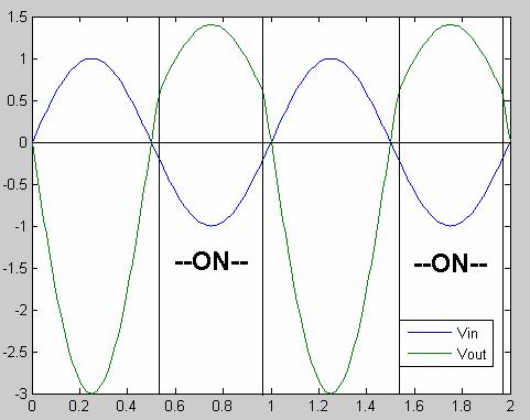
93
94
95
96
97
98
99
100
101
102 Midterm Solution for EE4 Sp 6 (Prepared by Josh Hug, jhug@eecs.berkeley.edu). esistive Circuits and Capacitors a. This is most easily solved by using the current divider rule: I 7 =I s /8 b. If we treat the two resistances in parallel as a ½ ohm resistor, we can use the voltage divider rule: = s * ½ / (½ ) * s = /3 s c. At the node of interest, we have I current coming in from the right, and I current leaving from the bottom, so we know that there must be I current leaving through the top. Thus, by Ohm s law, we know that = I*5. Furthermore, we also know by Ohm s law that =I. Using these two equations, we can find that = olts. Another way to solve this problem is to use KCL at the node: " # "! 5 " # "!! olts d. We know that for two capacitors in series, the charges are equal, and for two capacitors in parallel, the voltages are equal. If we treat the pair of C capacitors in parallel as a single 4C capacitor. Then we have the following equivalent circuit: We know that Q C =Q 4C, and C 4C = S, Q C =C* C, and Q 4C =4C* 4C. From Q C =C* C, Q 4C =4C* 4C, and Q C =Q 4C, we know that C = 4 4C Thus 4 4C 4C = S, so 4C = /5 * S, and C = 4/5 * S Q C =Q 4C = 4C/5 * S. One solution is to use the trick from homework 4. For < t < sec, we have the following circuit:
103 First we note that i L ( - )= i L ( )=, and i L (!)=/= Amps Next, we find the Thevenin resistance that the inductor sees, which is trivially Ohms. This gives us the time constant L/ = / = seconds Now that we know the initial current ( Amps), the steady state voltage ( Amps), and the time constant ( seconds), we use the shortcut from Homework 4 and get: I L ( t)! I! " e f " ( I " t / sec f " I ) e Amps i " t / $ For t > sec, we have the following circuit: First we note that i L ( - )= i L ( )= " / " " e! " e =.6 Amps To find i L (!), we can use superposition. From the volt source, i L (!) is increased by Amps. From the volt source, i L (!) is decreased by amp. Thus, i L (!)=-= Amp. Next, we find the Thevenin resistance that the inductor sees by zeroing out the independent sources, yielding the following circuit: This is just a ohm resistor in parallel with another ohm resistor, which means that the resistance the inductor sees is 5 ohms. Thus our time constant is /5=4 seconds.
104 So, again using the trick from homework 4, we have I L ( t)! I! " ( ".6) e! #.6e f " ( I f " I ) e "( t" ) / 4 "( t" sec) / 4sec i "( t" ) / $ Amps Another possible solution is to write the differential equations in both cases and solve. For the first case, we can use KL to find that: " I " I I L L # I L " I ' L " I ' L! ' L!! We first find the complementary solution I ( t)! Ke. Since we have our ' equation in the form I #$ I f ( t), we know that I C ( t)! Ke " t / sec Amps. L L! Next we can find the particular solution by guessing that our solution is of the form I P ( t)! A* f ( t) # B * f '( t)! A. Plugging this into our differential equation above, we get that A=, or A=. Finally, we know that I()=, so we find I()= I ( ) # I ()! K #!, or C C " t /$ " t / sec K=-. Thus, our final solution for < t < is I( t)! " e Amps. For the second part of the problem, we write a new differential equation using KCL at our node of interest. (We could also write two KL equations and add them). P Doing this, we obtain: L " L # L # #! % '! LI L ' ' I L " I L # I # # ' ' I " # I # # I! 4I 4I L ' L ' L " # I # I L L L! L! L L!
105 Since our equation is in the form I ' L #$ I L! f ( t), we know that our "( t"sec) / sec complementary solution is of the form I LC ( t)! Ke 4 Amps. Next we find the particular solution. As above, we assume that plug this into our differential equation, finding that A=. L ( t)! I P A, and Now we add our particular and complementary solution and have "( t" that ) / 4 " I L! Ke #. To find K, we know that I L ()! " e!. 6A, so "(" / 4 I )! Ke ) L ( #! K #!. 6A, and therefore K=.6A. Thus our final solution is I L ( t)! #.6e "( t" sec) / 4sec Amps There are many more possible solutions, such as using separation of variables, etc, 3. a. For t <, the circuit has been closed for a long time, and since we have a DC source, we can perform DC steady state analysis. We treat the capacitor as an open circuit, and the inductor like a short. Thus, we find " 5 that I L! 5/ 5,! Amps, and since the inductor acts like a short, C! olts. b. One method is to write KCL at the node, take the derivative of both sides, and reorganize the terms, as shown below: L " cos( t) ' L # CL # %! L ' L # sin( t) '' L # CL #! L ' L '' L sin( t) # L #! " C LC C '' ' # #! " sin( t) L L L c. Since, our equation is in the form & &!, '!, (!!! ', we know that Therefore, the complementary/transient solution is: "& t "& t C ( t)! Ke # Kte olts
106 d. Critically damped e. We assume a solution of the form ( t)! Acos( t) Bsin( t) ( t)! Acos( t) # Bsin( t) ' ( t)! " Asin( t) # B cos( t) p P '' P ( t)! " Acos( t) " Bsin( t) p # Then we plug them into our equation from part b, and get: " A cos( t) " Bsin( t) " Asin( t) # B cos( t) # Acos( t) # Bsin( t)! " sin( t) By collecting sine and cosine terms, we find the following: -ABA= -B-AB = - From the first equation we find that B=. Plugging B= into the second equation, we get -A=-, or A=. Thus our particular solution ( t) cos( t) p! f. We obtain the complete solution by adding the particular solution and the complementary solution, so we have: " t " t ( t)! Ke # Kte # cos( t) To find the constants, we can first use the initial condition v()=, and obtain: ()! K e # K e # cos()! K #! K! " To find K, we know that i L ( - )= i L ( "5 )= Amps. However, to use this information directly, we d need an equation for IL(t). Instead, it s easier to find i C ( # " ). Note: i C ( ) ) i C ( )!! At time, we can write KCL at node L, which gives us: # L ( ) cos() # I 5 " # ( ) # ( # C I L We also know the following facts: )!
107 I L L ( ( # # )! )! I C L ( # )! C " ( )! " ( )! " 5 Amps So our above KCL equation becomes: " " 5 # # I ( ) # " 5 C Amps! 5 This gives us: I C ( # )! -4/5 * -5 amps " 6 " t " t " t Next, we find I C ( t)! CC '( t)! ( e # K e " K te " sin( t)), and thus : " 6 " 5 ()! ( # K )! " 4 / 5* I C ( # K ( # K K! " 9 )! " 4 / 5 )! " 8 Thus, we have our final solution: " t / sec " t / sec L ( t)! " e " 9te # cos( t) olts
108 UNIESITY OF CALIFONIA AT BEKELEY EECS Department EECS 4, Spring 6 Prof. Chang-Hasnain Midterm # April 6, 6 Total Time Allotted: 8 minutes Total Points:. This is a closed book exam. However, you are allowed to bring two pages (8.5 x ), double-sided notes. No electronic devices, i.e. calculators, cell phones, computers, etc. 3. SHOW all the steps on the exam. Answers without steps will be given only a small percentage of credits. Partial credits will be given if you have proper steps but no final answers. 4. Draw BOXES around your final answers. 5. emember to put down units. Points will be taken off for answers without units. 6. NOTE: *= -6 ; k= 3 ; M= 6 Last (Family) Name: First Name: Student ID: Lab Session: Dis. Session: Signature: Score: Problem ( pts) Problem (35 pts): Problem 3 (5 pts): Problem 4 (3 pts): Total Page of 5
109 UNIESITY OF CALIFONIA AT BEKELEY EECS Department.( pts) Match the transfer function to the Bode plot. Each transfer function matches to exactly one Bode plot. Also, there is no partial credit for this question. a. H d. ( f )! jf -. /, H ( f )! jf # jf - #.5. # /, b. e. H ( f )!. / H jf f )! jf -. /, ( - #, # c. H ( f )! jf # Mark your answer here Magnitude Plot (db) 4 b e c a d Frequency (Hz) Page of 5
110 UNIESITY OF CALIFONIA AT BEKELEY EECS Department Mark your answer here Phase Plot (degrees) -5 - e d a b c Frequency (Hz) For the magnitude plot, we first split the list into first- and second-order Bode plots. The first order Bode plots have a -db/decade slope, and the second-order Bode plots have a - 4dB/decade slope. Looking at the breakpoints of the first-order Bode plots, we see that (c) has a breakpoint at f = Hz, and that (d) has a breakpoint at f = Hz. Looking at the size of the humps/peaks of the second-order Bode plots, decreasing values of zeta gives rise to a larger peak. (Note that technically speaking, (b) is two first-order terms but we can think of it as having a zeta = ). Page 3 of 5
111 UNIESITY OF CALIFONIA AT BEKELEY EECS Department From this, we have that the magnitude plots match as: (b), (e), (c), (a), (d). For the phase plot, we again split the list into first- and second-order terms. For first-order terms, the phase plot is -45 degrees at the breakpoint. For second order terms, decreasing values of zeta gives rise to a sharper phase transition. Page 4 of 5
112 UNIESITY OF CALIFONIA AT BEKELEY EECS Department.(35 pts) The circuit schematic for a functional block known as a lead compensator is: = " C =* F C =* F C =* F = " C =* F in out a (5 pts) Let = /() ohms, = /() ohms, C = uf, and C = uf. Show that the transfer function of the circuit shown above is: jf # H (f )! jf # Method : all at once -! ) in " I. # / j' C, ! ; I.! I. /, /, / j' C, / j' C - " " I. #! out ; I! out / j' C, -. # / j' C, ) " I " I j' C j' C 3) -, j' C - C ; I! I.! I. j' C C /, / -, C 3) I! out. - " / C, -. # / j' C, C - " out 3-4 Combine with ): in " # 6! 5/ C, -6 j' 7/ C, 5 8. # 6 57 / j' C, 68 Page 5 of 5
113 UNIESITY OF CALIFONIA AT BEKELEY EECS Department -. # C - j' C out " /,.! ; / C, - in. # / j' C, f - -. C # j f * F j 9 out j' # # j' C # :.... /, /,! " /,! "! " /,! /, in - 9 j' C # : - - f - -. C # j f * F j j'.. #. #. /, / /, /, /,, Method : Two Inverters out j' C in f # # ( )( ) # j! "! "! "! " j # ' C j f * F j' C # out j' C # j' C 3 4 f -! "! "! " # j f ( )( * F)! " j in. # /, j' C f j # out f -! " ; " j in f. #! f # j /, j # Method 3: Solve in stages: in " " out out j' C! ;! " in # # j' C j' C j'c # in " " out out j' C! ;! " in # j' C j' C j' C.. then same analysis as above.. then same analysis as above Page 6 of 5
114 UNIESITY OF CALIFONIA AT BEKELEY EECS Department b ( pts) In the following table, write the magnitude and phase values for H(f) for f=hz, f= Hz, very low f values ( f < Hz ) and very high f values ( f < = Hz ). These answers only need to be within.5 times the correct answer (but only because of rounding errors or sketching inaccuracies that you might have. Do not use the straight line approximation if it will cause your answer will be off from the exact value by more than.5 times). Note terms in red should be f, not '. Was announced during midterm f value (Hz) log H(') > H(') ery low f ( f < Hz ) 3dB 39.7 deg f = Hz 7dB 39.7 deg f = Hz db deg ery high f ( f < = Hz ) db deg Given terms: tan - (.) = 5.7 deg tan - (.5) = 6.6 deg tan - () = 45 deg tan - () = 63.4 deg tan - () = 84.3 deg 3 f # f -4 3 f Magnitude: log H ( f )! log 5/, 6! log # " log # f - 6 7/, 8 7/ 5. # 6 6 7/, 8 " f - " f - Phase: tan. " tan. /, /, , 8 For f=hz, becomes 3dB db = 3dB For f=hz, becomes db 3dB = 7dB Low f becomes db db 3 f High f becomes log 5/, 6 db!! 5 f /, 8 " " For f=hz, becomes 9 : 9 : " " For f=hz, becomes 9 : 9 : " " For f->, becomes tan 9: " tan 9:! A " " For f-> infinity, becomes 9 : 9 : tan " tan.! 45A " 5.7A! 39.3A tan " tan! 84.3A " 45A! 39.3A tan = " tan =! 9A " 9A! A Page 7 of 5
115 UNIESITY OF CALIFONIA AT BEKELEY EECS Department c (8 pts) Sketch the Bode plot of this transfer function. Sketch BOTH the magnitude and phase plot. Make sure to label the slopes of segments, the two break points of the transfer function, the low frequency magnitude, the high frequency magnitude, and the highest value on the phase plot. Be as accurate as you can, i.e., do not use the straight line approximation except as a starting guide if you wish for plotting the actual transfer function. 6 Bode Plot 4 Magnitude (db) Phase (degrees) Frequency - log scale Page 8 of 5
116 UNIESITY OF CALIFONIA AT BEKELEY EECS Department slope=db/dec slope=db/dec slope=~db/dec BP=Hz BP=Hz BP=Hz BP=Hz Page 9 of 5
117 UNIESITY OF CALIFONIA AT BEKELEY EECS Department 3.(5 pts) Find the unknown values in the circuits below. For the diodes, use the.8 ON- OFF model: If I_d <, then the diode is open or OFF If I_d =, then the diode is open or OFF If I_d >=, then the diode is a.8 source or ON If I_d >, then the diode is a.8 source or ON a. (5 pts) Find I_a in the circuit below: diode is off, 5 diode and I_a diode are on. I_a = 5 ".8 ".8! 34mA b. (5 pts) Find I_b in the circuit below: Page of 5
118 UNIESITY OF CALIFONIA AT BEKELEY EECS Department ) I_(ohm) = ; I_=mA (I_ is current in left branch) ) I_(ohm)-.8 = I_=9mA (I_) is current in right branch with diode) So I_b=I_I_=9mA c. (5 pts) Let _ = ohms and _ = ohms. Find _c in the circuit below, in terms of _ and _: =# =# C =# =# ) I() I() = ) I()= Page of 5
119 UNIESITY OF CALIFONIA AT BEKELEY EECS Department ) #! I ) I() I() = c ) I( ) = c " ) C! I # 3) c I() = I() (on far right opamp both voltages same) " 3 ) c C = # # - c. "! " # / #, # # ; 9 : ;! 9 " : c -.! " / #, # c Page of 5
120 UNIESITY OF CALIFONIA AT BEKELEY EECS Department 4.(3 pts) Consider the circuit shown below, in which the C time constant is very long compared to the period T of the input IN (t). Use the Ideal Diode model: If D <, then the diode is OFF and does not pass current (I D =) If I D >=, then the diode is ON and D = D is the voltage drop across the diode and I D is current through the diode. D = OUT in this problem. Analyze the following circuit. Given IN (t)= m sin(bt/t) for t>, and C (t= - )=. C - IN I D m IN - OUT T T 3T - t - m (a) (8 pts) Sketch C (t)? Label all key values. The capacitor is initially able to charge up, since _out starts at and so the diode is a short. However, the capacitor is not able to discharge through the diode since the diode is an open when reverse biased. Thus, the capacitor discharges through the resistor. Since the C constant is large, we have either: Or: (b) (8 pts) Sketch OUT (t)? Label all key values. Simple application of KL gives that _out = _in _c. The respective sketches of _out are: Page 3 of 5
121 UNIESITY OF CALIFONIA AT BEKELEY EECS Department OUT T T 3T t Or: OUT T T 3T t Note the concavity of the curves above. (c) (8 pts) Explain what is happening for different time duration. The capacitor is initially able to charge up, since _out starts at and so the diode allows current flow in the positive direction. However, the capacitor is not able to discharge through the diode since the diode is an open when reverse biased. Thus, the capacitor discharges through the resistor. Since the C time constant is large, the capacitor will discharge very slowly (in the limit it will not discharge at all). When _C matches _in, then _out is and so the diode will again allow the capacitor to charge up. We repeat this process. Page 4 of 5
122 UNIESITY OF CALIFONIA AT BEKELEY EECS Department (d) (6 pts) Sketch I D (t)? Label all key values. Or: Page 5 of 5
123 Last (Family) Name First Name Student ID Discussion Session EECS 4, Spring 6 Closed-book Quiz # Prof. Chang-Hasnain Total Time: 5 minutes Total Points:. No electronic devices, i.e. calculators, cell phones, computers, etc.. SHOW all the steps on the exam.. (4 pts) (a) Express in terms of,, a, and s s - a - and a are parallel. We only care about the voltage across them both, so when analyzing the circuit, we can treat their total resistance as eq = ( ; a ) /( # a ). - eq Then the circuit just looks like a simple voltage divider. So! s ;.. eq / #, Or: a! s ; # # a a (b) (3 pts) Set a to open circuit. What is? Just looking at the equation above, if we set equation becomes: a < =! s ; # (the definition of an open circuit), then the Which is the standard equation for a simple voltage divider circuit. We get the same result of course if we just look at the circuit with a taken out, and use the voltage divider equation. These equations are important for your labs, because it shows exactly what happens when we put a
124 Last (Family) Name First Name Student ID Discussion Session voltmeter with some finite input resistance into a circuit! Think of a as being the input resistance of a voltmeter, which is measuring the voltages in a voltage divider circuit. You can see by the equation in part (a) that we ll end up getting a slightly altered answer. We often assume voltmeters are perfect open circuits, but they really have a resistance on the order of mega-ohms. So, when we place them in a circuit, we have to be careful that we aren t affecting the rest of the circuit. In this example, if we are using typical resistor values for and (k for example), and the input resistance of our voltmeter ( a ) is M, we only affect the result by around.4%, basically negligible. But if we were using higher values for and, like M also, then we change by 33%, a huge difference! (c) (5 pts) Comparing in case (a) and (b). (which one is bigger?) By inspection, we can see by the equation in part (a), that as we increase a, we increase. So by KL, is bigger in case (a) Physically speaking, since this is a voltage divider circuit, the potential from the source is split in proportion to each resistance in the loop. So in the case where a is finite (case a), the effective total resistance of and a is lower than just alone (case b), so is bigger in case a. (d) (5 pts) Comparing in case (a) and (b). Again, since we get rid of a in part (b) (make it an open circuit), we increase the total resistance in that section of the voltage divider circuit, so is bigger in part (b).
125 Last (Family) Name First Name Student ID Discussion Session EECS 4, Spring 6 Closed-book Quiz #: February 4, 6 Prof. Chang-Hasnain Total Time: 5 minutes Total Points:. No electronic devices, i.e. calculators, cell phones, computers, etc.. SHOW all the steps on the exam.. (5 pts) (a) Express out in terms of,,, D, L, g m and s " s IN gm IN D L " out This circuit is easier than it may look at first. The single wire connecting the two loops doesn t really have any effect except to provide something like a ground wire between the two sections of the circuit. You can always arbitrarily make one of the nodes a ground node for any circuit if it isn t already labeled. So this ends up just looking like two separate grounded circuits. You can also notice that you can t have charge building up on one side of the circuit. Charge in these passive circuits is conserved. Even when charge is stored on a capacitor, you still have Q on one plate and Q on the other. OK, so for the actual analysis: is to. So we can make that eq = /( ). So in = s * eq / ( eq o ) since this is just a voltage divider circuit. Again, for the right side of the circuit, D is to L, so we can combine them into eq = D L /( D L ). Then since we have a voltage controlled current source and a resistor in one loop, we can easily figure out the voltage from ohm s law. = - I, I=g m IN. Careful of the sign convention here. It s negative since the current is flowing from the to signs on the out resistor. out! " g m s eq eq eq # o
126 Last (Family) Name First Name Student ID Discussion Session and substituting in: out! " - D L gms.. / D # L,/ # -. # o # /, It s usually good to try to substitute values in at the last step to keep the algebra simple. -, (b) (3 pts) For the load resistor L, what is the Thevenin equivalent voltage th and Thevenin equivalent resistance th? The right side of the circuit is already set up like a Thevenin equivalent current source and resistor. We know I sc = - g m IN (remember the sign convention again), and th = D in this configuration. th doesn t change for either case, and th = - D g m IN which is equal to (looking at our IN expression above:! " g th D m S -. # /, -. # o / #, (a) ( pts) At t= the switch is opened, prior to that, the switch had been closed for a long, long time. is a battery, what are Ic and c at t<? I t= c C - c
127 Last (Family) Name First Name Student ID Discussion Session If the switch is closed for a very long time, the circuit is in steady state (no signals are varying with time at this point). So the capacitor acts like an open circuit (since basically our values are all Hz at this point). So no current can be flowing in the loop (Ic=) and since must consequently be, then C = (b) ( pts) What are Ic and c when t goes to infinity? When the switch opens, no current flows. The charge that was on C stays on C. So at t=infinity, C =, and I C =.
128 Last (Family) Name First Name Student ID Discussion Session EECS 4, Spring 6 Closed-book Quiz #3: March 4, 6 Prof. Chang-Hasnain Total Time: 5 minutes Total Points:. No electronic devices, i.e. calculators, cell phones, computers, etc.. SHOW all the steps on the exam. = CDE out. You are given the circuit on the right. a) (3 pts) What are in and out in phasors? Write them in terms of '. in =3cos ('t/6) - C=u F in in phasor form is just in =3!3". The phasor form for out can be found using in and the transfer function for out as shown: out j' C 3> 3A 3! in! > A! > A!! > A " # # j' C # j' *s # ' > tan (') # ' j' C " (3 tan ( )) " ' Note I omitted the second term in the last two steps. To be more clear, the final answer with proper units would be something like out 3! > A " # (' *sec) ' " (3 tan ( *sec)) b) (5 pts) What is the break point frequency in Hz? The break frequency is just when out = out-max /sqrt(). So looking at the magnitude of out, the break point f B in Hz occurs when: 3 3!! #! # (' ) f B! Hz ; (' ) ; B ' B B rad s
129 Last (Family) Name First Name Student ID Discussion Session c) (5 pts) What type of filter is this? This is a low pass filter. emember, an easy way to tell is to think of what happens when the input is Hz, and when the input is #$%. At Hz, a capacitor acts like an open circuit so out is maximum. At #Hz, capacitors act like a short circuit, so out is. Hence, it passes the low frequency signals. H! (d) (3 pts) The transfer function is 9 : function. Plot x-y plot, where of the line as x>>. out '. Plot the magnitude Bode Plot of the transfer in y! log H (') and x = log 'FDDLabel y at x<<,, and the slope The transfer function is written above: H (')! # j' * s We already know the break angular frequency which is ' B! rad. So this is the point where the graph s switches from a slope of to a slope of -db/decade. We can do a quick sanity check and note that if we compare '=rad/s and '=rad/s, indeed H(w) drops by a factor of for a frequency that s about times higher than the break point. Hence, since the plot is of per decade above the break frequency. y! log H ('), the slope is -db 4 x<< slope= ' B, y=-3db (can approximate as for plot) *log H(') D - -4 x>> slope=-db/dec log(') At x<<, y is. At x= (w=), the break point, we can approximately draw the plot at y=, but
130 Last (Family) Name First Name Student ID Discussion Session really this is the 3dB point, so the y value is exactly -3dB. At x>>, the slope is labeled as - db/decade. (e) (3 pts) Plot phase Bode plot of the transfer function. Plot x-y plot where y! >H (') and x = log 'FDDDLabel y at x<<,, and the slope of the line as x>>. For the phase plot, we know the phase portion of the transfer function is > H (') =tan - (w*s) At frequencies w<<w B, the phase is just tan - (~) = ". At frequency w=w B, the phase is - tan - ()=&45' At frequencies w>>w B, the phase is just - tan - (infinity)= -9". So we draw the low frequency part up to / th of w B and the high frequency part down to w B and then connect them across the phase point for w=w B x<< slope= - ' B, y=-45a >H(') x>> slope= log(') When x<<, the value of y is 3 degrees. At x=, the y value is exactly -5 degrees. At x>>, the slope is zero, as shown in this plot.
131 Last (Family) Name First Name Student ID Discussion Session Hints: EECS 4, Spring 6 Closed-book Quiz #4: April 7, 6 Prof. Chang-Hasnain Total Time: 5 minutes Total Points: No electronic devices, i.e. calculators, cell phones, computers, etc. Gauss s Law de dx G! H Poisson Equation di( x) 5 E( x)! "!. 65 dx 8. p-n junction. You are given the space charge diagram on the right. a) ( pts) Express x in terms of x, N A and N D Since the sum of the total charges on each side has to equal, you can write qn D x -(qn A x ) = Charge density G9x) qn D x x -qn A x x = N A x /N D b) ( pts) Plot electric field E(x) vs. distance x. Assuming the H! is the permittivity of the material Label your plot. By Gauss Law, E( x)! G( x) H % dx So we just draw the integral of the plot of p(x) Since this is a square function, E(x) ends up looking like a triangle E(x) min = qn x H D " or qn Ax " H This is a plot of the electric field in the x direction so the Electric field is actually pointing to the left in this junction. c) ( pts) Plot electrostatic potential (x) vs. distance x. Label your plot. (x) = "% E( x) dx So you just have to draw the negative of the integral of your previous plot. Since the E field is zero outside the junction, the voltage is constant outside the junction too
132 emember, potential has an arbitrary ground. We ll say that the p-side is volts. So that makes the voltage on the n (right) side equal to the opposite of the area under the E(x) plot above. This is just " qn ( ) Dx qndx x x ( x ) J # J" H! H # x The voltage in the middle of the plot (x=) is just half the triangle: qn Dx qn x " J x J "! H H D d) ( pts) If what is described here is the depletion region of a pn junction, which side is n- side? Which is p-side? The left side is the p-side, the right side is the n-side. You can tell by the plot of charge density in the depletion region. The p-side has extra holes, which go to the other side and leave negatively charged atoms. The opposite occurs on the n-side (e) ( pts) If I connect the positive side of a battery to the x > x side, which direction will the current flow? If you connect a battery positive terminal to a point beyond x, you are connecting it to the n- side, so it is reversed bias, so no current will flow.
133 Given the circuit on the left and the load line analysis for i D and v DS on the right figure. DD 8 GS =5 3 k v G D i D I D (ma) GS =4 v S GS =3 GS = (a) ( pts) Determine DD, D DS () The load line plot tells us the voltage across the D to S terminals of the transistor. So we can see that if we cut the current to zero (open circuit, essentially as if we removed the transistor completely), then the voltage across those terminals would be. Since we said I=, the voltage across D and the 5 resistor are So DD = If we short the terminals, we see I D =ma. So we know that ma( D 5)= 5 = ma * D So 5/mA = D = 5 (b) (5 pts) If i D = 9 ma, tn = what is v S? What is v G? What is? If i D =9mA, we know that S = 9mA * 5 by ohm s law, so s =.5 To know GS, we need to use the load line analysis figure. We already know I D, so we need to determine what our DS and from that we can figure out GS. D = 9mA*5W = 7.75 So DS = = 5.5 So you can see on the plot above, that where I DS =9mA and DS =5.5 cross, the gate-source voltage of the transistor, GS, is equal to 4. So GS = 4 So the voltage of G is equal to GS S = 6.5 Since no current flows through the base, we can determine the thinking of and the 3k resistor as a voltage divider. 3
134 6.5 = # 3k ; = 5k (c) (5 pts) If i D = 4 ma, tn = what is v S? What is v G? What is? Just like before, if i D =4mA, we know S = 4mA * 5ohm =, D = 4mA*5ohm = 9, So DS = 9- = 8 So looking at the plot again, GS = 3, so G = GS S = 4 4 = # 3k ; = k (d) ( pts) Draw the new load line on the graph below when DD =5. What is the new i D? 8 6 GS =5 4 I D (ma) GS =4 GS =3 GS = DS () If the voltage changes to 5, then the open circuit voltage is still 5, and the closed circuit current is reduced by half since we cut the voltage in half. The slope of the line also has to stay the same since we didn t change the resistance in our equivalent circuit. I DS will of course be reduced, but the actual value depends on the choice of. 4
135 UNIESITY OF CALIFONIA AT BEKELEY EECS Department EECS 4, Spring 6 Prof. Chang-Hasnain Final Exam May 9, 6 Total Time Allotted: 8 minutes Total Points:. This is a closed book exam. However, you are allowed to bring three pages (8.5 x ), double-sided notes. No electronic devices, i.e. calculators, cell phones, computers, etc. 3. SHOW all the steps on the exam. Answers without steps will be given only a small percentage of credits. Partial credits will be given if you have proper steps but no final answers. 4. Draw BOXES around your final answers. 5. emember to put down units. Points will be taken off for answers without units. 6. NOTE:!= -6 ; k= 3 ; M= 6 Last (Family) Name: First Name: Student ID: Lab Session: Dis. Session: Signature: Score: Problem (3 pts) Problem (55 pts): Problem 3 ( pts): Problem 4 ( pts): Problem 5 ( pts): Problem 6 (55 pts): Total Page of 9
136 UNIESITY OF CALIFONIA AT BEKELEY EECS Department a. ( pts) Solve for in terms of s and v = Page of 9
137 UNIESITY OF CALIFONIA AT BEKELEY EECS Department b. (i) ( pts) Solve for node voltages and = = Page 3 of 9
138 UNIESITY OF CALIFONIA AT BEKELEY EECS Department b (ii) ( pts) Find the Norton equivalent current ( I N ) and resistance ( N ) for the circuit above (i) between and as shown: I N = N = Page 4 of 9
139 UNIESITY OF CALIFONIA AT BEKELEY EECS Department a) By combining the resistors, we can get a circuit that s a s, A resistor and two five ohm resistor in parallel(i.e..5 ohm). So this is a voltage divider, we can say that _ across the.5 ohm resistor as =s*(.5)/(.5)=s*(5/7) Use another voltage divider across the 4 and the equivalent resistance of 4//4//4//4=, =*(/5) =s(5/7)(/5)=s/7 b) Write KCL at and, and x=-: At node : A=(-)/[-(-)]/5/5! A=*(//5/5/5)*(-/-/5)! A=*(/)*(-7/3) At node : A=(-)/[-(-)]//5! A=*(//-//5)*(-//)! A=*(/5)*(/) Solve for and, =/37 =7/37 c) The open circuit oltage th=- and from part (b) this is -=/37-7/37=-7/37 The short circuit current Isc is obtained by shorting and, i.e -=, and x=. edraw the circuit after zeroing out the dependant voltage source, the circuit looks like the following: A 5# 5# # A 5# where: 5#//5#=5/4#, #//5#=/3# At node, A = /(5/4#)Isc At node, A=/(/3#)-Isc And =, sum the above two equations, 3A=/(5/4#) /(/3#) ==9/7 Substitue into the first equation In=Isc=A-/(5/4!) = -7/7 A n=th/in=7/37! Page 5 of 9
140 UNIESITY OF CALIFONIA AT BEKELEY EECS Department. (55 pts) Find the transfer function (from in to out ) of the circuit given below. Note that in and out are both referenced to ground. (For parts (a) through (f), write the relationships in terms of labeled values (like,, C, etc. ) a) ( pts) Use KCL to find the relationship between a and b in the subsection below: b) ( pts) Use KCL to find the relationship between a, b, and c in the subsection below: Page 6 of 9
141 UNIESITY OF CALIFONIA AT BEKELEY EECS Department c) ( pts) Using voltage divider, find the relationship between a and out in the subsection below: d) ( pts) Use KCL to find the relationship between d and out in the subsection below: e) (5 pts) Use KCL to find the relationship between in, c, and d in the subsection below: Page 7 of 9
142 UNIESITY OF CALIFONIA AT BEKELEY EECS Department f) ( pts) Combine the relationships from parts (a)-(e) to figure out the transfer function from in to out. You need not simplify your final solution. However, make sure to EXPLICITLY note when and where you use parts a,b,c,d,e. Make your work very clear! a. Simple application of KCL, in conjunction with the summing point constraints (SPC) yields that a / b /(/jwc ) =. This implies that a = -(jw* *C ) b. 5 for KCL 3 for SPC for math (- incorrect sign) b. Once again, using KCL and the SPC gives that c / b / a / =. This implies that c = - a b. 5 for KCL 3 for SPC for math (- incorrect sign) c. The voltage divider equation, and the SPC immediately gives that out = (/jwc )/((/jwc ) 3 )* a = /( jw*c * 3 )* a. 5 for oltage Divider/KCL 3 for SPC for math (- incorrect sign) d. Using KCL and the SPC, we get out / 5 d /((/jwc 3 ) 6 ) =. This implies that d = -( jw*c 3 * 6 )/(jw*c 3 * 5 )* out. 5 for KCL 3 for SPC for math (- incorrect sign) e. This, is the same as b. 5 for doing the same thing as in (b) or noting that the problem is the same as (b) or: for KCL for SPC for math f. There are several ways to do this, including some quite clever ways. The most straightforward is to merely do a series of substitutions. Combining equations (a) and (b) gives c = b *(jw* *C - ). Next, using equation (c) gives c = _out*(jw* *C )*(jw*c * 3 ). Next, consider equations (d) and (e). Combining these two blocks gives in = - c ( jw*c 3 * 6 )/(jw*c 3 * 5 )* out. From the relationship above, we can write that in = out *(-(jw* *C )*(jw*c * 3 ) ( jw*c 3 * 6 )/(jw*c 3 * 5 )). Thus, our final answer is that out / in = (-(jw* *C )*(jw*c * 3 ) ( jw*c 3 * 6 )/(jw*c 3 * 5 ))^(-). 4 for the correct connection of the blocks 3 for math 3 for giving a final answer Page 8 of 9
143 UNIESITY OF CALIFONIA AT BEKELEY EECS Department 3. ( pts) For the following circuits (i) write the truth table (ii) write the logic function as either a sum of products or product of sums. (a) DD D F A B C (b) DD A A B B C C F Page 9 of 9
144 UNIESITY OF CALIFONIA AT BEKELEY EECS Department Problem 3 The truth tables and logic functions are as follows: a) Note that when a high input is received at A, B, or C, the corresponding NMOS transistor turns on. When all transistors are off, no current can flow through the resistor, so F stays at the high voltage. When a transistor is on, it behaves almost as a short, so F goes to the low voltage. A B C F F # A" B " C The logic function is also known as NO. b) In this case, high inputs activate NMOS transistors and turn off PMOS transistors. Low inputs activate PMOS transistors and turn off NMOS transistors. The output follows a complete path either to the high voltage, or to ground, and assumes the corresponding voltage value, for any given input set. A B C F F # A" $ B & C% Note: we didn t require that the form of the expression be simplified completely. Any expression accurately describing the truth table was accepted for full credit. Page of 9
145 UNIESITY OF CALIFONIA AT BEKELEY EECS Department 4. ( pts) You are given the space charge diagram on the right. )( x) # qn, x ( x ( x, where # ' qn ( x, x #, everywhere else N D D A ( x (, ' x ) # ' N A x Charge density )$x) x qn D x x -qn A x Hints: Gauss s Law de dx ) # * Poisson Equation d ( x) E( x) # ' dx a) ( pts) Plot electric field E(x) vs. distance x. Assuming the *! is the permittivity of the material Label your plot. Label the axes as well as important points (both x and E(x) values at important points). b) ( pts) Plot electrostatic potential (x) vs. distance x. Label your plot. Label the axes as well as important points (both x and (x) values at important points). Page of 9
146 UNIESITY OF CALIFONIA AT BEKELEY EECS Department Problem 4 a) Part A required the use of Gauss Law in order to determine the electric field. Given the provided charge density plot, we obtain the following plot of electric field. Note that because - N A x = N D (x x ), we know that the integral over the charge density from x to x evaluates to zero, so E(x ) = E(x ). By a simple area calculations, we obtain the key value in the plot below. E(x) X X X x qn Ax E$ % # * b) Part B required the use of the Poisson Equation to determine the electric potential. The result is that change in electric potential is given by the negative of the integral over the electric field graph. Because the graph for E(x) is piecewise linear, this is again doable by hand. By some additional area calculations, we obtain the values in the plot below. (x) $ 3 $ X X X $ x As absolute voltage has no meaning, we focus only on the voltage differences outlined above. By geometric area calculations (A = l*w for rectangles, A = (/)b*h for triangles): qn A x qn $ %, #, A ' xx qn, #, A $ x ' x %$' x %, 3 # * * * Page of 9
147 UNIESITY OF CALIFONIA AT BEKELEY EECS Department 5 ( pts) Given the circuit on the left and the load line analysis for I D and D on the right figure. I D (ma) S I D D Diode Characteristics D () -.5 Load Line (a) ( pts) Determine the values of S, (b) ( pts) What are the solutions of D and I D for this circuit? Page 3 of 9
148 UNIESITY OF CALIFONIA AT BEKELEY EECS Department Problem 5 This problem was an exercise in interpreting a load-line characteristic plot. a) By inspection, the load line intersects the voltage axis at = -5. Given that the load line represents s and, which are arranged in Thevenin circuit form, this intersection gives the open circuit voltage s. We can also observe the value of I sc at -.4mA. Then, oc ' 5 # # #. 5k- #, s # ' 5 I sc '.4mA b) To determine I D and D, we can take the coordinates of the intersection point between the I characteristic of the diode and the load line. By KL the voltages must match, and by KCL the currents must match. By inspection, the current at this intersection is -.ma. Also, the voltage at the intersection is between -4 and -3. We can calculate this voltage explicitly, as follows: # I & s D D $ '.ma*.5k-% # 3. D # s ' I D # ' 5 ' ' 75 # ' 3.75, I # '. ma D D Page 4 of 9
149 UNIESITY OF CALIFONIA AT BEKELEY EECS Department 6. (55 pts) Analyze the following NMOS circuit. K= ma/ and t = a. ( pts) Using KL, write the equation of I DS as a function of DS. b. ( pts) Draw the load line on the following diagram. Page 5 of 9
150 UNIESITY OF CALIFONIA AT BEKELEY EECS Department c. ( pts) By using your load line plot or by using the equation for current through an NMOS, Find GSQ, I DSQ, DSQ d. (5 pts) Draw the small signal model e. ( pts) Find A v, the small signal voltage gain Page 6 of 9
151 UNIESITY OF CALIFONIA AT BEKELEY EECS Department Problem 6 a. ( pts) Using KL, write the equation of Ids as a function of ds. Solution: =-=, therefore source= Setup KCL at the drain node: (-ds)/kohm=ids (ds/kohm) Ids (ma) = (-ds)/kohm b. At Ids=, the ds=5v, and at ds=, the Ids=mA from part a. c. By using your load line plot or by using the equation for current through a MOSFET, Find GSQ, I DSQ, DSQ Solution: The Q point is where the gs=3v, from voltage divider rule, we know gs=v (3/37) =3volts. dsq=3v (can read of the plot) Ids=4mA by substituting the gs and ds into Ids(mA) = (-ds)/kohm or solve Ids=K(gs-t)^=K(3-)^=4mA Page 7 of 9
152 UNIESITY OF CALIFONIA AT BEKELEY EECS Department d) To get the small signal model we ground the DC source, replace the capacitor by a short, and replace the MOSFET by a dependent current source. Note: It was an extremely common mistake (>7%) for people to merge the S node and the ground node. While the op-amp does indeed force the S node to ground, it is still a distinct node! (In other words, if you write KCL at S, you get different equations than if you write it at node S. In other words again, the op-amp does not act like a wire. The book refers to this voltage copying behavior as a virtual short ) e) Let the current through the output resistor be called I o, with the positive direction from left to right (into the op-amp). Clearly v o =I o * K. To find I o, we just use some basic circuit analysis principles. First, we write KCL at node D, and get that d /K ds /K g m gs =. Since gs = in, and S=, we can rewrite KCL as: d /K d /K4 ms in =, which gives us d = - in. We know that I o will be the sum of the current out of the dependent source, and the current from D to S through the resistor. We get the current through the resistor using Ohm s law, and get that I ds_through_resistor = d /K= - in ma. Furthermore I ds_through_current_source =4 in ma. Thus, I o =I ds_through_resistor I ds_through_current_source = 4 in in ma = in ma. Thus v o = in, so the gain is. Sorry this problem was so difficult. I really didn t think (and still don t think) it s so bad, but Page 8 of 9
153 UNIESITY OF CALIFONIA AT BEKELEY EECS Department then again I have been teaching this class for a year. It s alright, though, only 4 or 5 people got the last part right, so nobody really suffered. - Josh Page 9 of 9
154 UNIESITY OF CALIFONIA AT BEKELEY EECS Department EECS 4, Spring 5 Prof. Chang-Hasnain Midterm # March 3, 5 Total Time Allotted: 8 minutes. This is a closed book exam. However, you are allowed to bring one page (8.5 x ), double-sided notes. No electronic devices, i.e. calculators, cell phones, computers, etc. 3. Numerical answers within a factor of.5 will not get points deducted, provided the steps are all correct and the errors are due to the lack of a calculator. (e.g. if the correct answer is, the acceptable range will be.67~.5). 4. SHOW all the steps on the exam. Answers without steps will be given only a small percentage of credits. Partial credits will be given if you have proper steps but no final answers. 5. Write your answers in the spaces (lines, boxes or plots) provided. 6. emember to put down units. Points will be taken off for answers without units. 7. NOTE: nh= -9 H; pf= - F; GHz= 9 Hz; MHz= 6 Hz Last (Family) Name: First Name: Student ID: Signature: Score: Problem ( pts) Problem ( pts): Problem 3 (3 pts): Problem 4 (3 pts): Total pts Page of
155 UNIESITY OF CALIFONIA AT BEKELEY EECS Department : A voltage source with voltage is connected to N identical resistors with resistance. (a) All of the resistors are connected in parallel, as in Figure a. What is the equivalent resistance eq? What is the total power consumed in the resistors? - = - eq N identical resistors Fig. a Solution: The resistors are in parallel so: N N = = eq n= eq = N Thus, the total power dissipated is: P = = N eq Answer: eq = /N Power = N / Page of
156 UNIESITY OF CALIFONIA AT BEKELEY EECS Department (b) All the resistors are all connected in series, as in Figure b. What is the equivalent resistance eq? What is the total power consumed in the resistors? - N identical resistors = - eq Fig. b Solution: The resistors are in series so: eq = N Thus, the total power dissipated is: P = = N eq Answer: eq = N Power = /N Page 3 of
157 UNIESITY OF CALIFONIA AT BEKELEY EECS Department. Equivalent circuit (a) What is equivalent resistance eq for points A-B? (b) What is the open circuit voltage across points A-B? (c) What is the short circuit current through points A-B? (d) Draw both Thevenin and Norton equivalent circuits. Ω 5 Ω 5 Ω Ω Ω Ω 5 Ω A 5 Ω B (a) To get the equivalent resistance, we short voltage source: Ω 5 Ω 5 Ω A Ω 5 Ω Ω Ω B 5 Ω Two in parallel is equivalent to one resistor of 5. So the equivalent circuit is: 5 Ω 5 Ω A 5 Ω 5 Ω Ω Ω B 5 Ω Two 5 in series and then in parallel with. =(5 5) = 5. So the equivalent circuit is: 5 Ω A 5 Ω Ω 5 Ω 5 Ω B Page 4 of
158 UNIESITY OF CALIFONIA AT BEKELEY EECS Department Again two 5 in series then in parallel with one resistor. =(5 5) = 5. So the equivalent circuit is: 5 Ω A 5 Ω 5 Ω B Finally, two 5 in series then in parallel with another 5. eq (b) Open circuit = (5 5) 5 = / 3Ω We set nodes C, D, E as shown below besides nodes A and B. Ω 5 Ω 5 Ω D C Ω E Ω Ω 5 Ω 5 Ω A B Figure Now we try to find the equivalent resistance to the right of D and E. Two 5 in series then in parallel with one, =(5 5) = 5. We get: Ω 5 Ω D Ω E C Ω 5 Ω 5 Ω B Figure To further simplify that, two 5 in series then in parallel with, =(5 5) = 5. We get: Ω 5 Ω D C Ω 5 Ω E Figure 3 Page 5 of
159 UNIESITY OF CALIFONIA AT BEKELEY EECS Department To further simplify, 5 in series then in parallel, =(5 5) = 5, we have: Ω D 5 Ω Then DE E 5 = = 5 3 From Figure 3, we know From Figure, we know CE CB Finally from Figure, we know = DE = CE = = = 5 5 oc = AB CB = 5 (c) I sc = oc eq = 5 3 = A 8 eq =/3 oc =5/ I sc =/8A Thevenin equivalent: Norton equivalent: 5/ /3 Ω A /8A /3 Ω A B B Page 6 of
160 UNIESITY OF CALIFONIA AT BEKELEY EECS Department 3. Transient Analysis: st order circuit (a) At t<, the switch is open and c =. At t=, the switch is closed towards the right. What is c (t)? (Hint: You can leave terms of the form e -x as they are) (b) At t= ps, the switch is closed towards the left and shall stay closed towards the left. What is c (t) when t> ps? (c) Qualitatively draw c (t) when t>. 5 Ω t= ps t= 5 Ω pf c - Solution: (a) Steady-state response: At DC steady-state, the capacitor behaves like an open circuit so we can redraw the circuit like so: No current flows in this circuit, so there is no voltage drop across the resistor and KL says that the steady state voltage is. Transient response: To see the natural response of the circuit, we turn off all power sources: Page 7 of
161 UNIESITY OF CALIFONIA AT BEKELEY EECS Department KL: where ( ) ( ) C t I t = dc ( t) I = C dt dc ( t) C ( t) = dt C This first-order linear differential equation gives solutions of the form t ( t) = Ke τ C Substituting into the homogeneous equation, we have: K t τ K t τ t τ e e = Ke = τ C τ C τ = C = 5ps Total response: From the above, we have that the total response is in the form: ( t) = Ke C t 5ps And since the voltage across a capacitor must be continuous, we have the initial condition: ( ) = K = C K = t e t 5ps C ( ) = (b) The analysis here is much the same as part (a). Steady-state response: C = -. Page 8 of
162 UNIESITY OF CALIFONIA AT BEKELEY EECS Department Transient response: t ( t) = Ke τ C τ = (5Ω 5 Ω )(pf) = ps Total response: ( t) = Le C t ps Note that this is equivalent to writing: ( t) = Me C ( t ps) ps So now when we use part (a) to find initial conditions: Page 9 of
163 UNIESITY OF CALIFONIA AT BEKELEY EECS Department ( ps) = e = e C ps 5ps ( ps) = Me = e C M = e (ps ps) ps t = e e ( t ps) ps C ( ) ( ) (c) <t< ps t 5ps c (t)= ( t) = e C t> ps ( t ps) ps c (t)= ( t) = ( e ) e C Draw c (t) vs t: Page of
164 UNIESITY OF CALIFONIA AT BEKELEY 4. Transient Analysis: nd order circuit At t=, the switch is closed. (a) What is the KL equation of the circuit in terms of c (t)? (b) Calculate ω, α, and ζ. Is the circuit underdamped, critically damped or overdamped? (c) What is the solution of c (t)? 3 (Hint: ω n = ω α = rad/s ) t = 5 - Ω C L EECS Department pf nh (a) = 5 L c d i = C dt c di dt c, L = L = LC d dt, d = i = C dt c d LC dt c d C dt c c = 5 or d dt d L dt c LC c c 5 = LC So d C dt d c c = 5 dt = (b) ω = LC rad/s α = L = 5 9 α ζ = = underdamped case ω (c) Since it s underdamped, the solution has the following form: c αt at = K e cosωnt K e sinωnt 5 Initial condition: there is no charge on the capacitor ( ) = So = K = K = 5 c 5 c Initial condition: there is no current in the circuit ( ) = = Page of i c d C dt t=
165 UNIESITY OF CALIFONIA AT BEKELEY EECS Department So i( ) αk 5 5 = α K ωn K = K = = = ω 3 n 3 3 c = 5e 9 5 t cos 3 t e 9 5 t sin 3 t 5 KL in terms of c (t): d c dt d c c = 5 dt ω = rad/s α = 9 5* ζ = / Damping case: underdamped t 5 t 3 c (t): c = 5e cos t e sin t 5 3 Page of
166 UNIESITY OF CALIFONIA AT BEKELEY EECS Department EECS 4, Spring 5 Prof. Chang-Hasnain Midterm # April 4, 5 Total Time Allotted: 8 minutes. This is a closed book exam. However, you are allowed to bring one page (8.5 x ), double-sided notes. No electronic devices, i.e. calculators, cell phones, computers, etc. 3. Numerical answers within a factor of.5 will not get points deducted, provided the steps are all correct and the errors are due to the lack of a calculator. (e.g. if the correct answer is, the acceptable range will be.67~.5). 4. SHOW all the steps on the exam. Answers without steps will be given only a small percentage of credits. Partial credits will be given if you have proper steps but no final answers. 5. Write your answers in the spaces (lines, boxes or plots) provided. 6. emember to put down units. Points will be taken off for answers without units. 7. Mobility chart is provided for your reference. Last (Family) Name: First Name: Student ID: Signature: Score: Problem (5 pts) Problem (5 pts): Problem 3 ( pts): Problem 4 (3 pts) Total pts

167 UNIESITY OF CALIFONIA AT BEKELEY EECS Department
Department of Electrical Engineering and Computer Sciences University of California, Berkeley. Final Exam Solutions
 Electrical Engineering 42/00 Summer 202 Instructor: Tony Dear Department of Electrical Engineering and omputer Sciences University of alifornia, Berkeley Final Exam Solutions. Diodes Have apacitance?!?!
analyse and design a range of sine-wave oscillators understand the design of multivibrators.
 INTODUTION In this lesson, we investigate some forms of wave-form generation using op amps. Of course, we could use basic transistor circuits, but it makes sense to simplify the analysis by considering
EE 40: Introduction to Microelectronic Circuits Spring 2008: Midterm 2
 EE 4: Introduction to Microelectronic Circuits Spring 8: Midterm Venkat Anantharam 3/9/8 Total Time Allotted : min Total Points:. This is a closed book exam. However, you are allowed to bring two pages
Low Power VLSI Circuits and Systems Prof. Ajit Pal Department of Computer Science and Engineering Indian Institute of Technology, Kharagpur
 Low Power VLSI Circuits and Systems Prof. Ajit Pal Department of Computer Science and Engineering Indian Institute of Technology, Kharagpur Lecture No. # 08 MOS Inverters - III Hello, and welcome to today
Refinements to Incremental Transistor Model
 Refinements to Incremental Transistor Model This section presents modifications to the incremental models that account for non-ideal transistor behavior Incremental output port resistance Incremental changes
UNIVERSITY OF CALIFORNIA, BERKELEY College of Engineering Department of Electrical Engineering and Computer Sciences
 UNIVERSITY OF CALIFORNIA, BERKELEY College of Engineering Department of Electrical Engineering and Computer Sciences EECS 40 Spring 2000 Introduction to Microelectronic Devices Prof. King MIDTERM EXAMINATION
Lecture 23: Negative Resistance Osc, Differential Osc, and VCOs
 EECS 142 Lecture 23: Negative Resistance Osc, Differential Osc, and VCOs Prof. Ali M. Niknejad University of California, Berkeley Copyright c 2005 by Ali M. Niknejad A. M. Niknejad University of California,
Dynamic circuits: Frequency domain analysis
 Electronic Circuits 1 Dynamic circuits: Contents Free oscillation and natural frequency Transfer functions Frequency response Bode plots 1 System behaviour: overview 2 System behaviour : review solution
EE292: Fundamentals of ECE
 EE292: Fundamentals of ECE Fall 2012 TTh 10:00-11:15 SEB 1242 Lecture 20 121101 http://www.ee.unlv.edu/~b1morris/ee292/ 2 Outline Chapters 1-3 Circuit Analysis Techniques Chapter 10 Diodes Ideal Model
Biasing BJTs CHAPTER OBJECTIVES 4.1 INTRODUCTION
 4 DC Biasing BJTs CHAPTER OBJECTIVES Be able to determine the dc levels for the variety of important BJT configurations. Understand how to measure the important voltage levels of a BJT transistor configuration
ECE 255, Frequency Response
 ECE 255, Frequency Response 19 April 2018 1 Introduction In this lecture, we address the frequency response of amplifiers. This was touched upon briefly in our previous lecture in Section 7.5 of the textbook.
Designing Information Devices and Systems I Fall 2018 Lecture Notes Note Introduction: Op-amps in Negative Feedback
 EECS 16A Designing Information Devices and Systems I Fall 2018 Lecture Notes Note 18 18.1 Introduction: Op-amps in Negative Feedback In the last note, we saw that can use an op-amp as a comparator. However,
Semiconductor Physics fall 2012 problems
 Semiconductor Physics fall 2012 problems 1. An n-type sample of silicon has a uniform density N D = 10 16 atoms cm -3 of arsenic, and a p-type silicon sample has N A = 10 15 atoms cm -3 of boron. For each
Chapter 8: Converter Transfer Functions
 Chapter 8. Converter Transfer Functions 8.1. Review of Bode plots 8.1.1. Single pole response 8.1.2. Single zero response 8.1.3. Right half-plane zero 8.1.4. Frequency inversion 8.1.5. Combinations 8.1.6.
Single-Time-Constant (STC) Circuits This lecture is given as a background that will be needed to determine the frequency response of the amplifiers.
 Circuits This lecture is given as a background that will be needed to determine the frequency response of the amplifiers.") Single-Time-Constant (STC) Circuits This lecture is given as a background that will be needed to determine the frequency response of the amplifiers. Objectives To analyze and understand STC circuits with
Single-Time-Constant (STC) Circuits This lecture is given as a background that will be needed to determine the frequency response of the amplifiers. Objectives To analyze and understand STC circuits with
Department of Electrical Engineering and Computer Sciences University of California, Berkeley. Final Exam: Friday, August 10, 2012
 Electrical Engineering 42/00 Summer 202 Instructor: Tony Dear Department of Electrical Engineering and Computer Sciences University of California, Berkeley Final Exam: Friday, August 0, 202 Last Name:
E40M Review - Part 1
 E40M Review Part 1 Topics in Part 1 (Today): KCL, KVL, Power Devices: V and I sources, R Nodal Analysis. Superposition Devices: Diodes, C, L Time Domain Diode, C, L Circuits Topics in Part 2 (Wed): MOSFETs,
6.012 Electronic Devices and Circuits Spring 2005
 6.012 Electronic Devices and Circuits Spring 2005 May 16, 2005 Final Exam (200 points) -OPEN BOOK- Problem NAME RECITATION TIME 1 2 3 4 5 Total General guidelines (please read carefully before starting):
Bipolar Junction Transistor (BJT) - Introduction
 - Introduction") Bipolar Junction Transistor (BJT) - Introduction It was found in 1948 at the Bell Telephone Laboratories. It is a three terminal device and has three semiconductor regions. It can be used in signal amplification
Bipolar Junction Transistor (BJT) - Introduction It was found in 1948 at the Bell Telephone Laboratories. It is a three terminal device and has three semiconductor regions. It can be used in signal amplification
2. The following diagram illustrates that voltage represents what physical dimension?
 BioE 1310 - Exam 1 2/20/2018 Answer Sheet - Correct answer is A for all questions 1. A particular voltage divider with 10 V across it consists of two resistors in series. One resistor is 7 KΩ and the other
Semiconductor Physics Problems 2015
 Semiconductor Physics Problems 2015 Page and figure numbers refer to Semiconductor Devices Physics and Technology, 3rd edition, by SM Sze and M-K Lee 1. The purest semiconductor crystals it is possible
Notes for course EE1.1 Circuit Analysis TOPIC 3 CIRCUIT ANALYSIS USING SUB-CIRCUITS
 Notes for course EE1.1 Circuit Analysis 2004-05 TOPIC 3 CIRCUIT ANALYSIS USING SUB-CIRCUITS OBJECTIVES 1) To introduce the Source Transformation 2) To consider the concepts of Linearity and Superposition
Field-Effect (FET) transistors
 transistors") Field-Effect (FET) transistors References: Barbow (Chapter 8), Rizzoni (chapters 8 & 9) In a field-effect transistor (FET), the width of a conducting channel in a semiconductor and, therefore, its current-carrying
Field-Effect (FET) transistors References: Barbow (Chapter 8), Rizzoni (chapters 8 & 9) In a field-effect transistor (FET), the width of a conducting channel in a semiconductor and, therefore, its current-carrying
Lecture 11: J-FET and MOSFET
 ENE 311 Lecture 11: J-FET and MOSFET FETs vs. BJTs Similarities: Amplifiers Switching devices Impedance matching circuits Differences: FETs are voltage controlled devices. BJTs are current controlled devices.
EE1-01 IMPERIAL COLLEGE LONDON DEPARTMENT OF ELECTRICAL AND ELECTRONIC ENGINEERING EXAMINATIONS 2013 ANALYSIS OF CIRCUITS. Tuesday, 28 May 10:00 am
 EE1-01 IMPERIAL COLLEGE LONDON DEPARTMENT OF ELECTRICAL AND ELECTRONIC ENGINEERING EXAMINATIONS 2013 ExamHeader: EEE/EIE PART I: MEng, Beng and ACGI ANALYSIS OF CIRCUITS Tuesday, 28 May 10:00 am Time allowed:
LCR Series Circuits. AC Theory. Introduction to LCR Series Circuits. Module. What you'll learn in Module 9. Module 9 Introduction
 Module 9 AC Theory LCR Series Circuits Introduction to LCR Series Circuits What you'll learn in Module 9. Module 9 Introduction Introduction to LCR Series Circuits. Section 9.1 LCR Series Circuits. Amazing
Prof. Anyes Taffard. Physics 120/220. Voltage Divider Capacitor RC circuits
 Prof. Anyes Taffard Physics 120/220 Voltage Divider Capacitor RC circuits Voltage Divider The figure is called a voltage divider. It s one of the most useful and important circuit elements we will encounter.
This is the 15th lecture of this course in which we begin a new topic, Excess Carriers. This topic will be covered in two lectures.
 Solid State Devices Dr. S. Karmalkar Department of Electronics and Communication Engineering Indian Institute of Technology, Madras Lecture - 15 Excess Carriers This is the 15th lecture of this course
REVISED HIGHER PHYSICS REVISION BOOKLET ELECTRONS AND ENERGY
 REVSED HGHER PHYSCS REVSON BOOKLET ELECTRONS AND ENERGY Kinross High School Monitoring and measuring a.c. Alternating current: Mains supply a.c.; batteries/cells supply d.c. Electrons moving back and forth,
6.1 Introduction
 6. Introduction A.C Circuits made up of resistors, inductors and capacitors are said to be resonant circuits when the current drawn from the supply is in phase with the impressed sinusoidal voltage. Then.
(Refer Slide Time: 03:41)
") Solid State Devices Dr. S. Karmalkar Department of Electronics and Communication Engineering Indian Institute of Technology, Madras Lecture - 25 PN Junction (Contd ) This is the 25th lecture of this course
Solid State Devices Dr. S. Karmalkar Department of Electronics and Communication Engineering Indian Institute of Technology, Madras Lecture - 25 PN Junction (Contd ) This is the 25th lecture of this course
ALTERNATING CURRENT. with X C = 0.34 A. SET UP: The specified value is the root-mean-square current; I. EXECUTE: (a) V = (0.34 A) = 0.12 A.
 V = (0.34 A) = 0.12 A.") ATENATING UENT 3 3 IDENTIFY: i Icosωt and I I/ SET UP: The specified value is the root-mean-square current; I 34 A EXEUTE: (a) I 34 A (b) I I (34 A) 48 A (c) Since the current is positive half of the time
ATENATING UENT 3 3 IDENTIFY: i Icosωt and I I/ SET UP: The specified value is the root-mean-square current; I 34 A EXEUTE: (a) I 34 A (b) I I (34 A) 48 A (c) Since the current is positive half of the time
IMPERIAL COLLEGE OF SCIENCE, TECHNOLOGY AND MEDICINE UNIVERSITY OF LONDON DEPARTMENT OF ELECTRICAL AND ELECTRONIC ENGINEERING EXAMINATIONS 2010
 Paper Number(s): E1.1 IMPERIAL COLLEGE OF SCIENCE, TECHNOLOGY AND MEDICINE UNIVERSITY OF LONDON DEPARTMENT OF ELECTRICAL AND ELECTRONIC ENGINEERING EXAMINATIONS 2010 EEE/ISE PART I: MEng, BEng and ACGI
Department of Electrical and Computer Engineering, Cornell University. ECE 3150: Microelectronics. Spring Due on March 01, 2018 at 7:00 PM
 Department of Electrical and Computer Engineering, Cornell University ECE 3150: Microelectronics Spring 2018 Homework 4 Due on March 01, 2018 at 7:00 PM Suggested Readings: a) Lecture notes Important Note:
Designing Information Devices and Systems I Spring 2015 Note 11
 EECS 16A Designing Information Devices and Systems I Spring 2015 Note 11 Lecture notes by Edward Wang (02/26/2015). Resistors Review Ohm s law: V = IR Water pipe circuit analogy: Figure 1: Water analogy
Chapter 2 - DC Biasing - BJTs
 Objectives Chapter 2 - DC Biasing - BJTs To Understand: Concept of Operating point and stability Analyzing Various biasing circuits and their comparison with respect to stability BJT A Review Invented
(Refer Slide Time: 1:41)
") Analog Electronic Circuits Professor S. C. Dutta Roy Department of Electrical Engineering Indian Institute of Technology Delhi Lecture no 13 Module no 01 Midband Analysis of CB and CC Amplifiers We are
Analog Electronic Circuits Professor S. C. Dutta Roy Department of Electrical Engineering Indian Institute of Technology Delhi Lecture no 13 Module no 01 Midband Analysis of CB and CC Amplifiers We are
Chapter 2. - DC Biasing - BJTs
 Chapter 2. - DC Biasing - BJTs Objectives To Understand : Concept of Operating point and stability Analyzing Various biasing circuits and their comparison with respect to stability BJT A Review Invented
I. Frequency Response of Voltage Amplifiers
 I. Frequency Response of Voltage Amplifiers A. Common-Emitter Amplifier: V i SUP i OUT R S V BIAS R L v OUT V Operating Point analysis: 0, R s 0, r o --->, r oc --->, R L ---> Find V BIAS such that I C
Lecture 04 Review of MOSFET
 ECE 541/ME 541 Microelectronic Fabrication Techniques Lecture 04 Review of MOSFET Zheng Yang (ERF 3017, email: yangzhen@uic.edu) What is a Transistor? A Switch! An MOS Transistor V GS V T V GS S Ron D
Chapter 13 Small-Signal Modeling and Linear Amplification
 Chapter 13 Small-Signal Modeling and Linear Amplification Microelectronic Circuit Design Richard C. Jaeger Travis N. Blalock 1/4/12 Chap 13-1 Chapter Goals Understanding of concepts related to: Transistors
Diodes. EE223 Digital & Analogue Electronics Derek Molloy 2012/2013.
 Diodes EE223 Digital & Analogue Electronics Derek Molloy 2012/2013 Derek.Molloy@dcu.ie Diodes: A Semiconductor? Conductors Such as copper, aluminium have a cloud of free electrons weak bound valence electrons
Lecture 37: Frequency response. Context
 EECS 05 Spring 004, Lecture 37 Lecture 37: Frequency response Prof J. S. Smith EECS 05 Spring 004, Lecture 37 Context We will figure out more of the design parameters for the amplifier we looked at in
(amperes) = (coulombs) (3.1) (seconds) Time varying current. (volts) =
 = (coulombs) (3.1) (seconds) Time varying current. (volts) =") 3 Electrical Circuits 3. Basic Concepts Electric charge coulomb of negative change contains 624 0 8 electrons. Current ampere is a steady flow of coulomb of change pass a given point in a conductor in
3 Electrical Circuits 3. Basic Concepts Electric charge coulomb of negative change contains 624 0 8 electrons. Current ampere is a steady flow of coulomb of change pass a given point in a conductor in
Networks and Systems Prof. V. G. K. Murti Department of Electrical Engineering Indian Institution of Technology, Madras
 Networks and Systems Prof. V. G. K. Murti Department of Electrical Engineering Indian Institution of Technology, Madras Lecture - 32 Network Function (3) 2-port networks: Symmetry Equivalent networks Examples
(Refer Slide Time: 1:49)
") Analog Electronic Circuits Professor S. C. Dutta Roy Department of Electrical Engineering Indian Institute of Technology Delhi Lecture no 14 Module no 01 Midband analysis of FET Amplifiers (Refer Slide
Analog Electronic Circuits Professor S. C. Dutta Roy Department of Electrical Engineering Indian Institute of Technology Delhi Lecture no 14 Module no 01 Midband analysis of FET Amplifiers (Refer Slide
Lecture 15: MOS Transistor models: Body effects, SPICE models. Context. In the last lecture, we discussed the modes of operation of a MOS FET:
 Lecture 15: MOS Transistor models: Body effects, SPICE models Context In the last lecture, we discussed the modes of operation of a MOS FET: oltage controlled resistor model I- curve (Square-Law Model)
Electronic Circuits 1. Transistor Devices. Contents BJT and FET Characteristics Operations. Prof. C.K. Tse: Transistor devices
 Electronic Circuits 1 Transistor Devices Contents BJT and FET Characteristics Operations 1 What is a transistor? Three-terminal device whose voltage-current relationship is controlled by a third voltage
Industrial Technology: Electronic Technology Crosswalk to AZ Math Standards
 Page 1 of 1 August 1998 1M-P1 Compare and contrast the real number system and its various subsystems with regard to their structural characteristics. PO 2 PO 3 2.0 Apply mathematics calculations. 2.1 Apply
Tunnel Diodes (Esaki Diode)
") Tunnel Diodes (Esaki Diode) Tunnel diode is the p-n junction device that exhibits negative resistance. That means when the voltage is increased the current through it decreases. Esaki diodes was named
Tunnel Diodes (Esaki Diode) Tunnel diode is the p-n junction device that exhibits negative resistance. That means when the voltage is increased the current through it decreases. Esaki diodes was named
ELECTRONIC SYSTEMS. Basic operational amplifier circuits. Electronic Systems - C3 13/05/ DDC Storey 1
 Electronic Systems C3 3/05/2009 Politecnico di Torino ICT school Lesson C3 ELECTONIC SYSTEMS C OPEATIONAL AMPLIFIES C.3 Op Amp circuits» Application examples» Analysis of amplifier circuits» Single and
Physics 4 Spring 1989 Lab 5 - AC Circuits
 Physics 4 Spring 1989 Lab 5 - AC Circuits Theory Consider the series inductor-resistor-capacitor circuit shown in figure 1. When an alternating voltage is applied to this circuit, the current and voltage
Sinusoidal Steady-State Analysis
 Chapter 4 Sinusoidal Steady-State Analysis In this unit, we consider circuits in which the sources are sinusoidal in nature. The review section of this unit covers most of section 9.1 9.9 of the text.
Inductive & Capacitive Circuits. Subhasish Chandra Assistant Professor Department of Physics Institute of Forensic Science, Nagpur
 Inductive & Capacitive Circuits Subhasish Chandra Assistant Professor Department of Physics Institute of Forensic Science, Nagpur LR Circuit LR Circuit (Charging) Let us consider a circuit having an inductance
Metal-Oxide-Semiconductor Field Effect Transistor (MOSFET)
") Metal-Oxide-Semiconductor ield Effect Transistor (MOSET) Source Gate Drain p p n- substrate - SUB MOSET is a symmetrical device in the most general case (for example, in an integrating circuit) In a separate
Metal-Oxide-Semiconductor ield Effect Transistor (MOSET) Source Gate Drain p p n- substrate - SUB MOSET is a symmetrical device in the most general case (for example, in an integrating circuit) In a separate
Basic Electronics Prof. Dr. Chitralekha Mahanta Department of Electronics and Communication Engineering Indian Institute of Technology, Guwahati
 Basic Electronics Prof. Dr. Chitralekha Mahanta Department of Electronics and Communication Engineering Indian Institute of Technology, Guwahati Module: 2 Bipolar Junction Transistors Lecture-4 Biasing
ENGN3227 Analogue Electronics. Problem Sets V1.0. Dr. Salman Durrani
 ENGN3227 Analogue Electronics Problem Sets V1.0 Dr. Salman Durrani November 2006 Copyright c 2006 by Salman Durrani. Problem Set List 1. Op-amp Circuits 2. Differential Amplifiers 3. Comparator Circuits
Symbol Offers Units. R Resistance, ohms. C Capacitance F, Farads. L Inductance H, Henry. E, I Voltage, Current V, Volts, A, Amps. D Signal shaping -
 Electrical Circuits HE 13.11.018 1. Electrical Components hese are tabulated below Component Name Properties esistor Simplest passive element, no dependence on time or frequency Capacitor eactive element,
Transistor amplifiers: Biasing and Small Signal Model
 Transistor amplifiers: iasing and Small Signal Model Transistor amplifiers utilizing JT or FT are similar in design and analysis. Accordingly we will discuss JT amplifiers thoroughly. Then, similar FT
Ver 3537 E1.1 Analysis of Circuits (2014) E1.1 Circuit Analysis. Problem Sheet 1 (Lectures 1 & 2)
 E1.1 Circuit Analysis. Problem Sheet 1 (Lectures 1 & 2)") Ver 3537 E. Analysis of Circuits () Key: [A]= easy... [E]=hard E. Circuit Analysis Problem Sheet (Lectures & ). [A] One of the following circuits is a series circuit and the other is a parallel circuit.
Ver 3537 E. Analysis of Circuits () Key: [A]= easy... [E]=hard E. Circuit Analysis Problem Sheet (Lectures & ). [A] One of the following circuits is a series circuit and the other is a parallel circuit.
Analog Integrated Circuit Design Prof. Nagendra Krishnapura Department of Electrical Engineering Indian Institute of Technology, Madras
 Analog Integrated Circuit Design Prof. Nagendra Krishnapura Department of Electrical Engineering Indian Institute of Technology, Madras Lecture No - 42 Fully Differential Single Stage Opamp Hello and welcome
Definitions. Decade: A ten-to-one range of frequency. On a log scale, each 10X change in frequency requires the same distance on the scale.
 Circuits II EECS 3220 Lecture notes on making Bode plots Definitions Network Transfer Function: The function H s Xout s X in s where X out represents the voltage or current response of the network to X
ECE3050 Assignment 7
 ECE3050 Assignment 7. Sketch and label the Bode magnitude and phase plots for the transfer functions given. Use loglog scales for the magnitude plots and linear-log scales for the phase plots. On the magnitude
Frequency Dependent Aspects of Op-amps
 Frequency Dependent Aspects of Op-amps Frequency dependent feedback circuits The arguments that lead to expressions describing the circuit gain of inverting and non-inverting amplifier circuits with resistive
AC Circuits Homework Set
 Problem 1. In an oscillating LC circuit in which C=4.0 μf, the maximum potential difference across the capacitor during the oscillations is 1.50 V and the maximum current through the inductor is 50.0 ma.
Direct-Current Circuits. Physics 231 Lecture 6-1
 Direct-Current Circuits Physics 231 Lecture 6-1 esistors in Series and Parallel As with capacitors, resistors are often in series and parallel configurations in circuits Series Parallel The question then
Direct Current (DC) Circuits
 Circuits") Direct Current (DC) Circuits NOTE: There are short answer analysis questions in the Participation section the informal lab report. emember to include these answers in your lab notebook as they will be
Direct Current (DC) Circuits NOTE: There are short answer analysis questions in the Participation section the informal lab report. emember to include these answers in your lab notebook as they will be
PHYS225 Lecture 9. Electronic Circuits
 PHYS225 Lecture 9 Electronic Circuits Last lecture Field Effect Transistors Voltage controlled resistor Various FET circuits Switch Source follower Current source Similar to BJT Draws no input current
Digital Electronics Part II - Circuits
 Digital Electronics Part - Circuits Dr.. J. Wassell Gates from Transistors ntroduction Logic circuits are non-linear, consequently we will introduce a graphical technique for analysing such circuits The
Electronics Fets and Mosfets Prof D C Dube Department of Physics Indian Institute of Technology, Delhi
 Electronics Fets and Mosfets Prof D C Dube Department of Physics Indian Institute of Technology, Delhi Module No. #05 Lecture No. #02 FETS and MOSFETS (contd.) In the previous lecture, we studied the working
Capacitors Diodes Transistors. PC200 Lectures. Terry Sturtevant. Wilfrid Laurier University. June 4, 2009
 Wilfrid Laurier University June 4, 2009 Capacitor an electronic device which consists of two conductive plates separated by an insulator Capacitor an electronic device which consists of two conductive
EE221 Circuits II. Chapter 14 Frequency Response
 EE22 Circuits II Chapter 4 Frequency Response Frequency Response Chapter 4 4. Introduction 4.2 Transfer Function 4.3 Bode Plots 4.4 Series Resonance 4.5 Parallel Resonance 4.6 Passive Filters 4.7 Active
6.012 Electronic Devices and Circuits
 Page 1 of 12 YOUR NAME Department of Electrical Engineering and Computer Science Massachusetts Institute of Technology 6.012 Electronic Devices and Circuits FINAL EXAMINATION Open book. Notes: 1. Unless
Chapter 4 Field-Effect Transistors
 Chapter 4 Field-Effect Transistors Microelectronic Circuit Design Richard C. Jaeger Travis N. Blalock 5/5/11 Chap 4-1 Chapter Goals Describe operation of MOSFETs. Define FET characteristics in operation
SIMPLE D.C. CIRCUITS AND MEASUREMENTS Background
 SIMPLE D.C. CICUITS AND MEASUEMENTSBackground This unit will discuss simple D.C. (direct current current in only one direction) circuits: The elements in them, the simple arrangements of these elements,
OPERATIONAL AMPLIFIER APPLICATIONS
 OPERATIONAL AMPLIFIER APPLICATIONS 2.1 The Ideal Op Amp (Chapter 2.1) Amplifier Applications 2.2 The Inverting Configuration (Chapter 2.2) 2.3 The Non-inverting Configuration (Chapter 2.3) 2.4 Difference
EE221 Circuits II. Chapter 14 Frequency Response
 EE22 Circuits II Chapter 4 Frequency Response Frequency Response Chapter 4 4. Introduction 4.2 Transfer Function 4.3 Bode Plots 4.4 Series Resonance 4.5 Parallel Resonance 4.6 Passive Filters 4.7 Active
Homework Assignment 09
 Homework Assignment 09 Question 1 (Short Takes) Two points each unless otherwise indicated. 1. What is the 3-dB bandwidth of the amplifier shown below if r π = 2.5K, r o = 100K, g m = 40 ms, and C L =
) t 0(q+ t ) dt n t( t) dt ( rre i dq t 0 u = = t l C t) t) a i( ( q tric c le E
 t 0(q+ t ) dt n t( t) dt ( rre i dq t 0 u = = t l C t) t) a i( ( q tric c le E") EE70 eview Electrical Current i ( t ) dq ( t ) dt t q ( t ) i ( t ) dt + t 0 q ( t 0 ) Circuit Elements An electrical circuit consists o circuit elements such as voltage sources, resistances, inductances
EE70 eview Electrical Current i ( t ) dq ( t ) dt t q ( t ) i ( t ) dt + t 0 q ( t 0 ) Circuit Elements An electrical circuit consists o circuit elements such as voltage sources, resistances, inductances
Vidyalankar S.E. Sem. III [EXTC] Analog Electronics - I Prelim Question Paper Solution
![Vidyalankar S.E. Sem. III [EXTC] Analog Electronics - I Prelim Question Paper Solution](/thumbs/90/101612294.jpg "Vidyalankar S.E. Sem. III [EXTC] Analog Electronics - I Prelim Question Paper Solution") . (a) S.E. Sem. [EXTC] Analog Electronics - Prelim Question Paper Solution Comparison between BJT and JFET BJT JFET ) BJT is a bipolar device, both majority JFET is an unipolar device, electron and minority
. (a) S.E. Sem. [EXTC] Analog Electronics - Prelim Question Paper Solution Comparison between BJT and JFET BJT JFET ) BJT is a bipolar device, both majority JFET is an unipolar device, electron and minority
CHAPTER 7 : BODE PLOTS AND GAIN ADJUSTMENTS COMPENSATION
 CHAPTER 7 : BODE PLOTS AND GAIN ADJUSTMENTS COMPENSATION Objectives Students should be able to: Draw the bode plots for first order and second order system. Determine the stability through the bode plots.
ECE 546 Lecture 10 MOS Transistors
 ECE 546 Lecture 10 MOS Transistors Spring 2018 Jose E. Schutt-Aine Electrical & Computer Engineering University of Illinois jesa@illinois.edu NMOS Transistor NMOS Transistor N-Channel MOSFET Built on p-type
SECTION: Circle one: Alam Lundstrom. ECE 305 Exam 5 SOLUTIONS: Spring 2016 April 18, 2016 M. A. Alam and M.S. Lundstrom Purdue University
 NAME: PUID: SECTION: Circle one: Alam Lundstrom ECE 305 Exam 5 SOLUTIONS: April 18, 2016 M A Alam and MS Lundstrom Purdue University This is a closed book exam You may use a calculator and the formula
CHAPTER.6 :TRANSISTOR FREQUENCY RESPONSE
 CHAPTER.6 :TRANSISTOR FREQUENCY RESPONSE To understand Decibels, log scale, general frequency considerations of an amplifier. low frequency analysis - Bode plot low frequency response BJT amplifier Miller
Designing Information Devices and Systems I Spring 2018 Lecture Notes Note 11
 EECS 16A Designing Information Devices and Systems I Spring 2018 Lecture Notes Note 11 11.1 Context Our ultimate goal is to design systems that solve people s problems. To do so, it s critical to understand
assess the biasing requirements for transistor amplifiers
 1 INTODUTION In this lesson we examine the properties of the bipolar junction transistor (JT) amd its typical practical characteristics. We then go on to devise circuits in which we can take best advantage
CS 436 HCI Technology Basic Electricity/Electronics Review
 CS 436 HCI Technology Basic Electricity/Electronics Review *Copyright 1997-2008, Perry R. Cook, Princeton University August 27, 2008 1 Basic Quantities and Units 1.1 Charge Number of electrons or units
Higher Physics. Electricity. Summary Notes. Monitoring and measuring a.c. Current, potential difference, power and resistance
 Higher Physics Electricity Summary Notes Monitoring and measuring a.c. Current, potential difference, power and resistance Electrical sources and internal resistance Capacitors Conductors, semiconductors
(Refer Time Slide: 1:35)
") Analog Electronic Circuits Prof. S. C. Dutta Roy Department of Electrical Engineering. Indian Institute of Technology Delhi Lecture No 04 Problem Session 1 On DC Analysis of BJT Circuits This is the fourth
Analog Electronic Circuits Prof. S. C. Dutta Roy Department of Electrical Engineering. Indian Institute of Technology Delhi Lecture No 04 Problem Session 1 On DC Analysis of BJT Circuits This is the fourth
Second-order filters. EE 230 second-order filters 1
 Second-order filters Second order filters: Have second order polynomials in the denominator of the transfer function, and can have zeroth-, first-, or second-order polynomials in the numerator. Use two
BIOEN 302, Section 3: AC electronics
 BIOEN 3, Section 3: AC electronics For this section, you will need to have very present the basics of complex number calculus (see Section for a brief overview) and EE5 s section on phasors.. Representation
Electronics for Analog Signal Processing - II Prof. K. Radhakrishna Rao Department of Electrical Engineering Indian Institute of Technology Madras
 Electronics for Analog Signal Processing - II Prof. K. Radhakrishna Rao Department of Electrical Engineering Indian Institute of Technology Madras Lecture - 14 Oscillators Let us consider sinusoidal oscillators.
Steady State Frequency Response Using Bode Plots
 School of Engineering Department of Electrical and Computer Engineering 332:224 Principles of Electrical Engineering II Laboratory Experiment 3 Steady State Frequency Response Using Bode Plots 1 Introduction
Homework Assignment 08
 Homework Assignment 08 Question 1 (Short Takes) Two points each unless otherwise indicated. 1. Give one phrase/sentence that describes the primary advantage of an active load. Answer: Large effective resistance
Physics 115. General Physics II. Session 24 Circuits Series and parallel R Meters Kirchoff s Rules
 Physics 115 General Physics II Session 24 Circuits Series and parallel R Meters Kirchoff s Rules R. J. Wilkes Email: phy115a@u.washington.edu Home page: http://courses.washington.edu/phy115a/ 5/15/14 Phys
Two-Port Networks Admittance Parameters CHAPTER16 THE LEARNING GOALS FOR THIS CHAPTER ARE THAT STUDENTS SHOULD BE ABLE TO:
 CHAPTER16 Two-Port Networks THE LEARNING GOALS FOR THIS CHAPTER ARE THAT STUDENTS SHOULD BE ABLE TO: Calculate the admittance, impedance, hybrid, and transmission parameter for two-port networks. Convert
Whereas the diode was a 1-junction device, the transistor contains two junctions. This leads to two possibilities:
 Part Recall: two types of charge carriers in semiconductors: electrons & holes two types of doped semiconductors: n-type (favor e-), p-type (favor holes) for conduction Whereas the diode was a -junction
Networks and Systems Prof. V. G. K. Murti Department of Electrical Engineering Indian Institute of Technology, Madras
 Networks and Systems Prof. V. G. K. Murti Department of Electrical Engineering Indian Institute of Technology, Madras Lecture - 34 Network Theorems (1) Superposition Theorem Substitution Theorem The next
E2.2 Analogue Electronics
 E2.2 Analogue Electronics Instructor : Christos Papavassiliou Office, email : EE 915, c.papavas@imperial.ac.uk Lectures : Monday 2pm, room 408 (weeks 2-11) Thursday 3pm, room 509 (weeks 4-11) Problem,
Homework 6 Solutions and Rubric
 Homework 6 Solutions and Rubric EE 140/40A 1. K-W Tube Amplifier b) Load Resistor e) Common-cathode a) Input Diff Pair f) Cathode-Follower h) Positive Feedback c) Tail Resistor g) Cc d) Av,cm = 1/ Figure