Physical Properties of Materials. 1. Electrical Properties 2. Optical Properties 3. Magnetic Properties
|
|
|
- Ezra Ferguson
- 5 years ago
- Views:
Transcription
1 Physical Properties of Materials 1. Electrical Properties 2. Optical Properties 3. Magnetic Properties 1
2 1. electrical properties 2
3 (1) electrical conduction in metals classical Model metallic bonds make free movement of valence electrons possible outer valence electrons are completely free to move between positive ion cores positive ion cores vibrate with greater amplitude with increasing temperature the motion of electrons are random and restricted in absence of electric field no net electron flow in presence of electric field, electrons attain directed drift velocity that is proportional to the applied field but in the opposite direction 3
 R: resistance of wire (Ω) electric resistivity A ρ = R l l: length of the conductor A: cross-sectional area of the conductor electric conductivity σ =")
4 Ohm s law electric current flow i is directly proportional to the applied voltage V and inversely proportional to resistance of the wire V i = R i: electric current (A) V: potential difference (V) R: resistance of wire (Ω) electric resistivity A ρ = R l l: length of the conductor A: cross-sectional area of the conductor electric conductivity σ = 1/ ρ 4
5 conductor σ > 10 7 (Ω m) -1 metals insulator σ ~ (Ω m) -1 polymer semiconductor Si, Ge ex. a wire whose diameter is 0.20 cm carries 20 A current, the maximum power is 4 W/m, calculate the minimum allowable conductivity of the wire P = iv =i 2 R R = ρ l / A σ = 1/ρ i 2 l (20 A) 2 (1 m) σ = = = (Ω m) -1 PA (4 W) π(0.001 m) 2 ex. Cu wire conducts 10A of current with maximum voltage drop of 0.4 V/m. what is the minimum diameter? R = V/i ρ = RA/ l = AV / i l σ = i l / AV (Ω m) -1 = (10 A)(1 m) / A (0.4 V) (10 A)(1 m) A = = m 2 (0.4 V) (Ω m) -1 d = 4 ( )/π = m microscopic Ohm's law J = E / ρ or J = σ E J: current density A/m 2 E: electric field V/m 5
 the electron flow in metal wire depends on the number of electrons per unit volume, the electronic charge (-1.")
6 drift velocity of electrons electrons are accelerated when electric field E is applied and collide with ion cores after a collision, they accelerate again electron velocity varies in a saw tooth manner drift velocity v d = μ E μ: electron mobility m 2 /(V s) the electron flow in metal wire depends on the number of electrons per unit volume, the electronic charge ( C), and the drift velocity of electrons the current density J = nev d direction of current flow is opposite to that of electrons 6
 ρ 0 o C: resistivity at 0 o C α T : coefficient of resistivity T: temperature of the")
7 electrical resistivity ρ total = ρ T + ρ r ρ T thermal component elastic waves (phonons) generated due to vibration of electron core scatter electrons resistivity increases with temperature ρ T = ρ 0 o C (1+ α T T) ρ 0 o C: resistivity at 0 o C α T : coefficient of resistivity T: temperature of the metal 7
8 ex. calculate the electrical resistivity of Cu at 132 o C ρ T = ρ 0 o C (1+ α T T) = ( ) = Ω m ρ r residual component due to structural imperfections like dislocations, grain boundaries, impurity atoms ρ r is almost independent of temperature alloying increases resistivity addition of various elements to Cu 8
.")
9 (2) energy-band model of electrical conduction valence electrons are delocalized, interact and interpenetrate each other sharply defined energy levels are broadened into wider regions called energy bands ex. Na has 1 valence electron (3s 1 ). there are N Na atoms, there are N distinct 3s 1 energy levels in 3s energy band energy bands Na is a good conductor since it has half filled outer 3s band, very little energy is required to 9 produce electron flow


10 energy-band diagrams for Na, Mg, and Al in insulators, electrons are tightly bound to the bonding atoms large energy gap E g separates lower filled valence band and upper empty conduction band to be available for conduction, the electron should jump the energy gap, which may as much as 6~7 ev (for diamond) 10


11 (3) intrinsic semiconductors semiconductors electrical conductivities are between good conductors and insulators. intrinsic semiconductors pure semiconductors and conductivities are determined by their inherent properties ex. Si and Ge sufficient energy is needed to excite valence electrons away from their bonding position bonding electron becomes a free conduction electron and leaves a hole behind both electrons and holes are charge carriers hole is attracted to negative terminal, electron to positive terminal 11


12 the motion of a hole in an electric field energy-band diagram for an intrinsic semiconductor such as pure Si (E g = 1.1 ev) quantitative relationship of electrical conduction current density J = nqv n * + pqv p * n: number of conduction electrons per unit volume p: number of conduction holes per unit volume q: absolute value of electron or hole charge (1.6 x C) 12 v n, v p : drift velocities of electrons and holes
 6.023 10 23 atoms 1 2.33 10 6 g ( )( )( ) mol 28.08 g/mol m 3 = 5.00 10 28 atoms/m 3 ex.")
13 J = σ E J nqv n * pqv p * σ = = + E E E v n /E: electron mobility μ n v p /E: hole mobility μ p σ = nqμ n + pqμ p for intrinsic semiconductor n = p = n i σ = n i q(μ n + μ p ) ex. calculate the number of Si atoms per m 3 (d = 2.33 Mg/m 3, atomic mass: 28.08) atoms g ( )( )( ) mol g/mol m 3 = atoms/m 3 ex. calculate the electrical resistivity of Si at 300 K σ = n i q(μ n + μ p ) = ( m -3 ) ( C) ( m 2 /V s) = Ω-1 m-1 ρ = 1/σ = Ω m 13
14 effect of temperature on intrinsic semiconductors the conduction band is completely empty at 0 o K at higher temperatures, valence electrons are excited to conduction bands conductivities increase with increasing temperature n i e -(E g E av )/kt n i : concentrations of electrons having energy to enter conduction band. E g : energy gap E av : average energy across gap k: Boltzmann's constant T: temperature E av = E g /2 n i e -(E g)/2kt σ = σ 0 e -(E g)/2kt σ 0 : constant depending on the mobility E g ln σ = ln σ 0-2kT E g can be determined from the slope of the plot of ln σ vs. 1/T for intrinsic semiconductor 14
15 ex. plot of ln σ vs. 1/T for Si ex. electrical resistivity of pure Si is Ω m at 27 o C, calculate its conductivity at 200 o C (E g = 1.1 ev, k = ev/k) E g ln σ = ln σ 0-2kT σ ev 1 1 ln = ( - ) σ ( ev/k) = σ 473 = e σ 300 = 2385(1/ ) = 1.04 Ω-1 m-1 15
 added to Si only 0.")
16 (4) extrinsic semiconductors have impurity atoms ( ppm) that have different valance characteristics (i) n type extrinsic semiconductors impurities donate electrons for conduction ex. group VA atoms (P, As, Sb) added to Si only ev of energy is required to remove the excess electron from its parent nucleus 16

17 (ii) p-type extrinsic semiconductors group IIIA atoms when added to silicon, a hole is created since one of the bonding electrons is missing when electric field is applied, electrons from the neighboring bond move to the hole boron atom gets ionized and hole moves towards negative terminal B, Al, Ga provide acceptor level energy and are hence called acceptor atoms 17

18 doping impurity atoms (dopants) are deposited into silicon by diffusion at C (iii) effect of doping on carrier concentration the mass action law at constant temperature np = n 2 i n i : intrinsic concentration of carriers in a semiconductor and a constant at a given temperature n, p : concentration of electrons or holes since the semiconductor must be electrically neutral N a + n = N d + p N a and N d are concentrations of negative acceptor ions and positive donor ions in a n-type semiconductor, N a = 0 and n >> p hence n n N d p n = n i2 /n n n i2 /N d 18 for p-type semiconductor n p = n i2 /p p n i2 /N a
19 typical carrier concentrations in intrinsic and extrinsic semiconductors Si at 300 K n i = carriers/m 3 for extrinsic Si doped with As at a typical concentration of impurity atoms/m 3 n n = electrons/m 3 p n = holes/m 3 ex. Si wafer doped with P atoms/m 3 calculate (a) the majority-carrier concentration, (b) the minority-carrier concentration, (c) the electrical resistivity of this n-type semiconductor at room temperature (assume complete ionization of the dopant atoms; and n i = m -3, μ n = m 2 /V s, μ p = m 2 /V s) (a) n n = electrons/m 3 (b) p n = ( m -3 ) 2 /10 21 m -3 = holes/m 3 (c) 1 1 ρ = = qn n μ n ( C)(0.135 m 2 /V s)(10 21 m -3 ) = Ω m 19
20 ex. P-doped Si wafer has an electrical resistivity of Ω mat 27 o C. assume μ n = m 2 /V s, μ p = m 2 /V s, (a) what is its majority-carrier concentration if complete ionization is assumed? (b) what is the ratio of P to Si atoms in this semiconductor? (a) this is an n-type semiconductor, the majoritycarrier is electron and the resistivity 1 1 ρ = hence n n = qn n μ n ρ qμ n 1 n n = ( Ω m)( C)(0.135 m 2 /V s) = electrons/m 3 (b) pure Si contains atoms/m 3 P/Si ratio = / = (iv) effect of total ionized impurity concentration as the concentration of impurities increase, mobility of carriers decrease 20
21 ex. Si is doped with B atoms/cm P atoms/cm 3 at 27 o C. Calculate (a) the equilibrium electron and hole concentrations, (b) the mobilities of electrons and holes, and (c) the electrical resistivity (n i = cm -3 ) (a) majority-carrier concentration p p N a N d = = holes/cm 3 minority-carrier concentration n p = n i2 /p p = ( ) 2 / = electrons/cm 3 (b) total impurity concentration = atoms/cm 3 check figure find μ n = 900 cm 2 /V s μ p = 300 cm 2 /V s (c) electrical resistivity 1 1 ρ = = qp p μ p ( C)(300 cm 2 /V s)( cm -3 ) = 5.2 Ω cm 21
22 (v) effect of temperature on electrical conductivity extrinsic range electrical conductivity increases with temperature as more and more impurity atoms are ionized exhaustion range temperature at which donor atom becomes completely ionized for n-type semiconductor saturation range acceptor atoms become completely ionized for p-type semiconductor beyond these ranges, temperature does not change conductivity substantially further increase in temperature results in intrinsic conduction becoming dominant and is called intrinsic range 22
23 to provide an exhaustion (or saturation) range at about room temperature is important since it provides temperature range that have essentially constant electrical conductivity ex. (a) As-doped Si (b) B-doped Si 23
24 (5) semiconductor devices (a) pn junction n-type and p-type silicon semiconductors are joined together formed by doping a single crystal of silicon first by n-type and then by p-type material majority carriers cross over the junction and recombine but the process stops later as electrons repelled by negative ions giving rise to depletion region under equilibrium conditions, there exists a barrier to majority carrier flow there is no net current flow 24
25 (b) biased an external voltage is applied to a pn junction reverse biased n-type is connected to the positive terminal of battery, electrons of n- type material and holes of p-type material move away from junction current resulting from majority carriers does not flow leakage current (of the order of μa) flows due to minority carriers 25
26 forward biased n-type is connected to the negative terminal and p-type to positive majority carriers are repelled to the junction and recombine and considerable current flows 26
27 (c) application of pn junction diode rectifier diodes converts alternating voltage into direct voltage (rectification) when AC signal is applied to diode, current flows only when p-region is positive and hence half way rectification is achieved signal can be further smoothed out by using other electronic devices breakdown diodes (zener diodes) in reverse bias, small leakage currents flow upon breakdown voltage is reached, reverse current increases rapidly electrons gain sufficient energy to knock more electrons from covalent bonds these are available for conduction in reverse bias 27

 collector collects electrons emitter base junction is forward biased and collector base")
28 (d) bipolar junction transistor (BJT) BJT consists of two pn junctions occurring sequentially on a single crystal can serve as current amplifier ex. npn BJT emitter emits electrons base controls flow of charge (0.1mm thick) collector collects electrons emitter base junction is forward biased and collector base junction is reverse biased small base current can be used to control large collector current 28
 microelectronic planar bipolar transistors ex.")

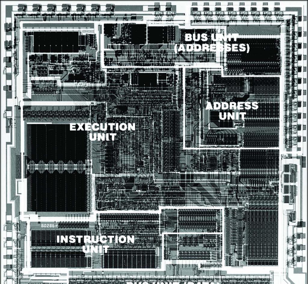
29 (6) microelectronics thousands of transistors on a chip of Si about 5 mm 2 and 0.2 mm thick (a) microelectronic planar bipolar transistors ex. planar bipolar npn transistor relatively large island of n-type silicon is formed first in a p-type Si substrate smaller island of p and n type silicon are created on larger n type island 29
30 (b) microelectronic planar field-effect transistor MOSFET (metal oxide semiconductor field effect transistor) NMOS n-type MOSFET PMOS p-type MOSFET ex. NMOS overall structure cross-sectional view two islands of n-type silicon are created in a substrate of p-type silicon source the contact where electrons enter drain the contact where electrons leave gate third contact, a layer of polysilicon 30
31 no voltage is applied to the gate, only a few electrons are attracted to the drain when a positive voltage is applied to the gate, electrons will flow between source and drain if there is positive voltage difference between them MOSFET is capable of current amplification MOSFET technology is the basis for most LSI digital memory circuits 31


32 (c) fabrication of microelectric integrated circuits laying out IC network photolithographic mask chrome mask emulsion mask 32


33 (i) photolithography the process by which microscopic pattern is transferred from a photomask to the silicon wafer surface step 2 wafer is coated with photoresist step 3 then exposed to UV light through photomask step 4 pattern of photoresist is left where mask is transparent step 5 wafer is immersed in hydrofluoric acid step 6 photoresist pattern is removed by other chemicals 33
34 (ii) diffusion technique impurity atoms are diffused into Si wafers at about 1000 ~ 1100 o C thin silicon dioxide patterns serve as masks to prevent dopant atoms from penetrating into silicon high concentration of dopant is deposited near surface in predeposit step in drive-in diffusion step, the wafers are placed in high temperature furnace and necessary concentration of dopant atoms at particular depth is attained. 34

35 (iii) ion implantation technique carried out at room temperature dopant atoms are ionized and accelerated to high energies through a high potential difference of KV on striking, ions embed in Si photoresist or SiO 2 is used to mask desired regions damage to Si lattice is caused but can be healed by annealing 35

36 (iv) MOS integrated circuit fabrication step 1 deposition of SiN 4 by CVD boron ions are implanted to suppress unwanted conduction SiO 2 layer is grown in inactive regions step 2 SiN 4 is removed by etchants step 3 insulating layer is deposited on wafer by CVD step 4 Al is deposited on wafer step 5 protective layer is deposited on entire surface 36
37 (v) NMOS integrated circuits fabrication 37
38 (vi) complimentary metal oxide semiconductor (CMOS) devices circuits containing both types of MOSFETs NMOS and PMOS made by isolating all NMOS devices with islands of p-type material. used in LSI circuits in microprocessors and computer memories. 38
 m 2 /(V s) constant carrier/m 3 IV A Si 1.10 0.135 0.048 5.4307 1.5 10 16 Ge 0.67 0.390 0.190 5.257 2.4 10 19 IIIA - GaP 2.25 0.030 0.015 5.450 V A GaAs 1.47 0.720 0.020 5.")
39 (7) compound semiconductors MX semiconductors are major compound semiconductors IIIA-VA and IIA-VIA electrical properties of intrinsic semiconductors at room temperature E g μ n μ p lattice n i Group Material ev m 2 /(V s) m 2 /(V s) constant carrier/m 3 IV A Si Ge IIIA - GaP V A GaAs GaSb InP InAs InSb IIA - ZnSe VI A ZnTe CdSe CdTe
 is the most important of all compound semiconductors advantages: higher mobility better radiation resistance ex.")
40 as molecular mass increases energy band gap decreases and electron mobility increases increasing ionic bonding character energy band gap increases and electron mobility decreases gallium arsenide (GaAs) is the most important of all compound semiconductors advantages: higher mobility better radiation resistance ex. (a) calculate the intrinsic electrical conductivity of GaAs at room temperature (b) what fraction of the current is carried by the electrons in GaAs at 27 o C? (a) σ = n i q(μ n + μ p ) = ( )( )( ) = (Ω m) -1 (b) σ n n i qμ n = = = σ n i q(μ n + μ p )
 dielectric constant parallel-plate capacitor q = CV or C = q/v C: capacitance (farad = coulomb/volt) area dimension A >> distance d A C = ε 0 d permittivity of free space ε 0 = 8.")
41 (8) electrical properties of ceramics used for electrical insulators for low- and high- voltage electric currents application in various types of capacitors piezoelectrics (a) basic properties of dielectrics (i) dielectric constant parallel-plate capacitor q = CV or C = q/v C: capacitance (farad = coulomb/volt) area dimension A >> distance d A C = ε 0 d permittivity of free space ε 0 = F/m a dielectric fills the space between plates κε 0 A C = d κ : dielectric constant 41
42 the energy stored in a capacity of a given volume at given voltage is increased by the factor of dielectric constant (ii) dielectric strength a measure of the ability of the material to hold energy at high voltage defined as voltage per unit length the maximum electric field that the dielectric can maintain without electrical breakdown commonly measured in volts/mil (1 mil = in) or kilovolts/mm (iii) dielectric loss factor κ tan δ dielectric loss angle δ ex. a parallel-plate capacitor made to store C at a potential of 8000 V separation distance = 0.30 mm, calculate the area of the plates if dielectric is (a) a 42 vacuum (κ = 1) and (b) aluminum (κ = 9)
43 κε 0 A Cd ( /8000)( ) C = A = = d κε 0 k ( ) (a) κ = 1 A = m 2 (b) κ = 9 A = m 2 (b) ceramic insulator materials electrical and mechanical properties make ceramic materials suitable for insulator applications (i) electrical porcelain 50% clay (Al 2 O 3.2SiO 2.2H 2 O) + 25% silica (SiO 2 ) + 25% feldspar (K 2 O.Al 2 O 3.6SiO 2 ) good green-body plasticity and a wide firing temperature disadvantage: high power-loss factor (ii) steatite porcelain 90% talc (3MgO.4SiO 2.H 2 O) + 10% clay good electrical insulator due to low powerloss factor, low moisture absorption, and good impact strength 43
 alumina ceramic Al 2 O 3 as the crystalline phase bonded with a glassy matrix has relatively high dielectric strength and low dielectric loss and relatively high strength")
44 (iii) fosterite chemical formula: Mg 2 SiO 4 has high resistivity and low electrical loss with increasing temperature has lower-loss dielectrica properties at high frequencies (iv) alumina ceramic Al 2 O 3 as the crystalline phase bonded with a glassy matrix has relatively high dielectric strength and low dielectric loss and relatively high strength 44
 after firing ceramic disk (ii) after applying Ag electrodes (iii) after soldering")
45 (c) ceramic materials for capacitors most common type: disk ceramic capacitors, consist mainly of BaTiO 3 and other additives dielectric constant formulation 325 BaTiO 3 + CaTiO 3 + low% Bi 2 Sn 3 O BaTiO 3 + low% CaZrO 3 and Nb 2 O BaTiO 3 + low% CaZrO 3 or CaTiO 3 + BaZrO 3 steps in manufacture: (i) after firing ceramic disk (ii) after applying Ag electrodes (iii) after soldering Pb (iv) after applying dipped phenolic coating 45
46 (d) ceramic semiconductors thermistor (thermally sensitive resistor) is used for temperature measurement and control negative temperature coefficient (NTC) resistance decreases with increasing temperature, as the temperature increases, the termistor becomes more conductive most commonly used for NTC thermistors: oxides of Mn, Ni, Fe, Co, Cu ex. Fe 3 O 4 mixed with MgCr 2 O 4 to adjust the resistivity 46


47 (e) ferroelectric ceramics ferroelectric ionic crystalline materials have unit cells that do not have a center of symmetry and contain small electric dipole industrially important material: BaTiO 3 > 120 o C regular cubic symmetrical perovskite structure < 120 o C (the Curie temperature) Ti 4+ and O 2- ions shift slightly in opposite directions the crystal structure changes from cubic to slightly tetragonal formation of ferroelectric domain 47

48 the piezoelectric (PZT) effect an effect by which mechanical forces can produce an electrical response, or electrical forces a mechanical response an excess of positive and negative charges at two ends in piezoelectric material when compressive stresses are applied, the length of the sample is reduced and the distance between the unit dipoles are reduced the overall dipole moment is reduced and the voltage difference between the ends is changed an electric field is applied across the ends, the charge density at each end will be changed it causes the change in dimensions in the 48 direction of the applied field

49 examples of industrial applications compression accelerator mechanical electrical ultrasonic cleaning transducer electrical mechanical 49
Chapter 1 Overview of Semiconductor Materials and Physics
 Chapter 1 Overview of Semiconductor Materials and Physics Professor Paul K. Chu Conductivity / Resistivity of Insulators, Semiconductors, and Conductors Semiconductor Elements Period II III IV V VI 2 B
ISSUES TO ADDRESS...
 Chapter 12: Electrical Properties School of Mechanical Engineering Choi, Hae-Jin Materials Science - Prof. Choi, Hae-Jin Chapter 12-1 ISSUES TO ADDRESS... How are electrical conductance and resistance
Electrical material properties
 Electrical material properties U = I R Ohm s law R = ρ (l/a) ρ resistivity l length σ = 1/ρ σ conductivity A area σ = n q μ n conc. of charge carriers q their charge μ their mobility μ depends on T, defects,
12/10/09. Chapter 18: Electrical Properties. View of an Integrated Circuit. Electrical Conduction ISSUES TO ADDRESS...
 Chapter 18: Electrical Properties ISSUES TO ADDRESS... How are electrical conductance and resistance characterized? What are the physical phenomena that distinguish? For metals, how is affected by and
Introduction to Semiconductor Physics. Prof.P. Ravindran, Department of Physics, Central University of Tamil Nadu, India
 Introduction to Semiconductor Physics 1 Prof.P. Ravindran, Department of Physics, Central University of Tamil Nadu, India http://folk.uio.no/ravi/cmp2013 Review of Semiconductor Physics Semiconductor fundamentals
Semiconductor Physics Problems 2015
 Semiconductor Physics Problems 2015 Page and figure numbers refer to Semiconductor Devices Physics and Technology, 3rd edition, by SM Sze and M-K Lee 1. The purest semiconductor crystals it is possible
Section 12: Intro to Devices
 Section 12: Intro to Devices Extensive reading materials on reserve, including Robert F. Pierret, Semiconductor Device Fundamentals Bond Model of Electrons and Holes Si Si Si Si Si Si Si Si Si Silicon
EE301 Electronics I , Fall
 EE301 Electronics I 2018-2019, Fall 1. Introduction to Microelectronics (1 Week/3 Hrs.) Introduction, Historical Background, Basic Consepts 2. Rewiev of Semiconductors (1 Week/3 Hrs.) Semiconductor materials
ESE 570: Digital Integrated Circuits and VLSI Fundamentals
 ESE 570: Digital Integrated Circuits and VLSI Fundamentals Lec 4: January 23, 2018 MOS Transistor Theory, MOS Model Penn ESE 570 Spring 2018 Khanna Lecture Outline! CMOS Process Enhancements! Semiconductor
CME 300 Properties of Materials. ANSWERS: Homework 9 November 26, As atoms approach each other in the solid state the quantized energy states:
 CME 300 Properties of Materials ANSWERS: Homework 9 November 26, 2011 As atoms approach each other in the solid state the quantized energy states: are split. This splitting is associated with the wave
Lecture 2. Semiconductor Physics. Sunday 4/10/2015 Semiconductor Physics 1-1
 Lecture 2 Semiconductor Physics Sunday 4/10/2015 Semiconductor Physics 1-1 Outline Intrinsic bond model: electrons and holes Charge carrier generation and recombination Intrinsic semiconductor Doping:
Semiconductors. SEM and EDAX images of an integrated circuit. SEM EDAX: Si EDAX: Al. Institut für Werkstoffe der ElektrotechnikIWE
 SEM and EDAX images of an integrated circuit SEM EDAX: Si EDAX: Al source: [Cal 99 / 605] M&D-.PPT, slide: 1, 12.02.02 Classification semiconductors electronic semiconductors mixed conductors ionic conductors
Introduction to Engineering Materials ENGR2000. Dr.Coates
 Introduction to Engineering Materials ENGR2000 Chapter 18: Electrical Properties Dr.Coates 18.2 Ohm s Law V = IR where R is the resistance of the material, V is the voltage and I is the current. l R A
ESE 570: Digital Integrated Circuits and VLSI Fundamentals
 ESE 570: Digital Integrated Circuits and VLSI Fundamentals Lec 4: January 29, 2019 MOS Transistor Theory, MOS Model Penn ESE 570 Spring 2019 Khanna Lecture Outline! CMOS Process Enhancements! Semiconductor
Semiconductors. Semiconductors also can collect and generate photons, so they are important in optoelectronic or photonic applications.
 Semiconductors Semiconducting materials have electrical properties that fall between true conductors, (like metals) which are always highly conducting and insulators (like glass or plastic or common ceramics)
Chapter 12: Electrical Properties. RA l
 Charge carriers and conduction: Chapter 12: Electrical Properties Charge carriers include all species capable of transporting electrical charge, including electrons, ions, and electron holes. The latter
The Science & Engineering of Materials Semiconductors. 주요반도체재료에서전자와홀의 mobility 대표적인값은? 어떤 carrier 가빠른지?
 18.6 Semiconductors 주요반도체재료에서전자와홀의 mobility 대표적인값은? 어떤 carrier 가빠른지? 18.6 Semiconductors [Fig. 18-16] - + When a voltage is applied to a semiconductor, the electrons move through the conduction band, while
collisions of electrons. In semiconductor, in certain temperature ranges the conductivity increases rapidly by increasing temperature
 1.9. Temperature Dependence of Semiconductor Conductivity Such dependence is one most important in semiconductor. In metals, Conductivity decreases by increasing temperature due to greater frequency of
smal band gap Saturday, April 9, 2011
 small band gap upper (conduction) band empty small gap valence band filled 2s 2p 2s 2p hybrid (s+p)band 2p no gap 2s (depend on the crystallographic orientation) extrinsic semiconductor semi-metal electron
n N D n p = n i p N A
 Summary of electron and hole concentration in semiconductors Intrinsic semiconductor: E G n kt i = pi = N e 2 0 Donor-doped semiconductor: n N D where N D is the concentration of donor impurity Acceptor-doped
Chapter 3 Basics Semiconductor Devices and Processing
 Chapter 3 Basics Semiconductor Devices and Processing Hong Xiao, Ph. D. www2.austin.cc.tx.us/hongxiao/book.htm Hong Xiao, Ph. D. www2.austin.cc.tx.us/hongxiao/book.htm 1 Objectives Identify at least two
16EC401 BASIC ELECTRONIC DEVICES UNIT I PN JUNCTION DIODE. Energy Band Diagram of Conductor, Insulator and Semiconductor:
 16EC401 BASIC ELECTRONIC DEVICES UNIT I PN JUNCTION DIODE Energy bands in Intrinsic and Extrinsic silicon: Energy Band Diagram of Conductor, Insulator and Semiconductor: 1 2 Carrier transport: Any motion
Electrical Properties
 Electrical Properties Electrical Conduction R Ohm s law V = IR I l Area, A V where I is current (Ampere), V is voltage (Volts) and R is the resistance (Ohms or ) of the conductor Resistivity Resistivity,
SEMICONDUCTORS. Conductivity lies between conductors and insulators. The flow of charge in a metal results from the
 SEMICONDUCTORS Conductivity lies between conductors and insulators The flow of charge in a metal results from the movement of electrons Electros are negatively charged particles (q=1.60x10⁻¹⁹ C ) The outermost
Electronic Devices & Circuits
 Electronic Devices & Circuits For Electronics & Communication Engineering By www.thegateacademy.com Syllabus Syllabus for Electronic Devices Energy Bands in Intrinsic and Extrinsic Silicon, Carrier Transport,
Silicon Detectors in High Energy Physics
 Thomas Bergauer (HEPHY Vienna) IPM Teheran 22 May 2011 Sunday: Schedule Silicon Detectors in Semiconductor Basics (45 ) Detector concepts: Pixels and Strips (45 ) Coffee Break Strip Detector Performance
Section 12: Intro to Devices
 Section 12: Intro to Devices Extensive reading materials on reserve, including Robert F. Pierret, Semiconductor Device Fundamentals EE143 Ali Javey Bond Model of Electrons and Holes Si Si Si Si Si Si Si
! CMOS Process Enhancements. ! Semiconductor Physics. " Band gaps. " Field Effects. ! MOS Physics. " Cut-off. " Depletion.
 ESE 570: Digital Integrated Circuits and VLSI Fundamentals Lec 4: January 3, 018 MOS Transistor Theory, MOS Model Lecture Outline! CMOS Process Enhancements! Semiconductor Physics " Band gaps " Field Effects!
Electro - Principles I
 Electro - Principles I Page 10-1 Atomic Theory It is necessary to know what goes on at the atomic level of a semiconductor so the characteristics of the semiconductor can be understood. In many cases a
ELECTRONIC I Lecture 1 Introduction to semiconductor. By Asst. Prof Dr. Jassim K. Hmood
 ELECTRONIC I Lecture 1 Introduction to semiconductor By Asst. Prof Dr. Jassim K. Hmood SOLID-STATE ELECTRONIC MATERIALS Electronic materials generally can be divided into three categories: insulators,
Unit IV Semiconductors Engineering Physics
 Introduction A semiconductor is a material that has a resistivity lies between that of a conductor and an insulator. The conductivity of a semiconductor material can be varied under an external electrical
! CMOS Process Enhancements. ! Semiconductor Physics. " Band gaps. " Field Effects. ! MOS Physics. " Cut-off. " Depletion.
 ESE 570: Digital Integrated Circuits and VLSI Fundamentals Lec 4: January 9, 019 MOS Transistor Theory, MOS Model Lecture Outline CMOS Process Enhancements Semiconductor Physics Band gaps Field Effects
CHAPTER 18: Electrical properties
 CHAPTER 18: Electrical properties ISSUES TO ADDRESS... How are electrical conductance and resistance characterized? What are the physical phenomena that distinguish conductors, semiconductors, and insulators?
Engineering 2000 Chapter 8 Semiconductors. ENG2000: R.I. Hornsey Semi: 1
 Engineering 2000 Chapter 8 Semiconductors ENG2000: R.I. Hornsey Semi: 1 Overview We need to know the electrical properties of Si To do this, we must also draw on some of the physical properties and we
1 Name: Student number: DEPARTMENT OF PHYSICS AND PHYSICAL OCEANOGRAPHY MEMORIAL UNIVERSITY OF NEWFOUNDLAND. Fall :00-11:00
 1 Name: DEPARTMENT OF PHYSICS AND PHYSICAL OCEANOGRAPHY MEMORIAL UNIVERSITY OF NEWFOUNDLAND Final Exam Physics 3000 December 11, 2012 Fall 2012 9:00-11:00 INSTRUCTIONS: 1. Answer all seven (7) questions.
Classification of Solids
 Classification of Solids Classification by conductivity, which is related to the band structure: (Filled bands are shown dark; D(E) = Density of states) Class Electron Density Density of States D(E) Examples
ELECTRONIC DEVICES AND CIRCUITS SUMMARY
 ELECTRONIC DEVICES AND CIRCUITS SUMMARY Classification of Materials: Insulator: An insulator is a material that offers a very low level (or negligible) of conductivity when voltage is applied. Eg: Paper,
Electrical Resistance
 Electrical Resistance I + V _ W Material with resistivity ρ t L Resistance R V I = L ρ Wt (Unit: ohms) where ρ is the electrical resistivity 1 Adding parts/billion to parts/thousand of dopants to pure
A semiconductor is an almost insulating material, in which by contamination (doping) positive or negative charge carriers can be introduced.
 positive or negative charge carriers can be introduced.") Semiconductor A semiconductor is an almost insulating material, in which by contamination (doping) positive or negative charge carriers can be introduced. Page 2 Semiconductor materials Page 3 Energy levels
Semiconductor A semiconductor is an almost insulating material, in which by contamination (doping) positive or negative charge carriers can be introduced. Page 2 Semiconductor materials Page 3 Energy levels
Electronics The basics of semiconductor physics
 Electronics The basics of semiconductor physics Prof. Márta Rencz, Gergely Nagy BME DED September 16, 2013 The basic properties of semiconductors Semiconductors conductance is between that of conductors
Lecture 1. OUTLINE Basic Semiconductor Physics. Reading: Chapter 2.1. Semiconductors Intrinsic (undoped) silicon Doping Carrier concentrations
 silicon Doping Carrier concentrations") Lecture 1 OUTLINE Basic Semiconductor Physics Semiconductors Intrinsic (undoped) silicon Doping Carrier concentrations Reading: Chapter 2.1 EE105 Fall 2007 Lecture 1, Slide 1 What is a Semiconductor? Low
Lecture 1 OUTLINE Basic Semiconductor Physics Semiconductors Intrinsic (undoped) silicon Doping Carrier concentrations Reading: Chapter 2.1 EE105 Fall 2007 Lecture 1, Slide 1 What is a Semiconductor? Low
Semiconductor physics I. The Crystal Structure of Solids
 Lecture 3 Semiconductor physics I The Crystal Structure of Solids 1 Semiconductor materials Types of solids Space lattices Atomic Bonding Imperfection and doping in SOLIDS 2 Semiconductor Semiconductors
Fabrication Technology, Part I
 EEL5225: Principles of MEMS Transducers (Fall 2004) Fabrication Technology, Part I Agenda: Microfabrication Overview Basic semiconductor devices Materials Key processes Oxidation Thin-film Deposition Reading:
Semiconductor Physics fall 2012 problems
 Semiconductor Physics fall 2012 problems 1. An n-type sample of silicon has a uniform density N D = 10 16 atoms cm -3 of arsenic, and a p-type silicon sample has N A = 10 15 atoms cm -3 of boron. For each
Lecture 2. Introduction to semiconductors Structures and characteristics in semiconductors
 Lecture 2 Introduction to semiconductors Structures and characteristics in semiconductors Semiconductor p-n junction Metal Oxide Silicon structure Semiconductor contact Literature Glen F. Knoll, Radiation
Lecture 2. Introduction to semiconductors Structures and characteristics in semiconductors
 Lecture 2 Introduction to semiconductors Structures and characteristics in semiconductors Semiconductor p-n junction Metal Oxide Silicon structure Semiconductor contact Literature Glen F. Knoll, Radiation
Chapter 4: Bonding in Solids and Electronic Properties. Free electron theory
 Chapter 4: Bonding in Solids and Electronic Properties Free electron theory Consider free electrons in a metal an electron gas. regards a metal as a box in which electrons are free to move. assumes nuclei
EECS143 Microfabrication Technology
 EECS143 Microfabrication Technology Professor Ali Javey Introduction to Materials Lecture 1 Evolution of Devices Yesterday s Transistor (1947) Today s Transistor (2006) Why Semiconductors? Conductors e.g
Electronic Circuits for Mechatronics ELCT 609 Lecture 2: PN Junctions (1)
") Electronic Circuits for Mechatronics ELCT 609 Lecture 2: PN Junctions (1) Assistant Professor Office: C3.315 E-mail: eman.azab@guc.edu.eg 1 Electronic (Semiconductor) Devices P-N Junctions (Diodes): Physical
Electronic Circuits for Mechatronics ELCT 609 Lecture 2: PN Junctions (1) Assistant Professor Office: C3.315 E-mail: eman.azab@guc.edu.eg 1 Electronic (Semiconductor) Devices P-N Junctions (Diodes): Physical
EE 446/646 Photovoltaic Devices I. Y. Baghzouz
 EE 446/646 Photovoltaic Devices I Y. Baghzouz What is Photovoltaics? First used in about 1890, the word has two parts: photo, derived from the Greek word for light, volt, relating to electricity pioneer
EECS130 Integrated Circuit Devices
 EECS130 Integrated Circuit Devices Professor Ali Javey 8/30/2007 Semiconductor Fundamentals Lecture 2 Read: Chapters 1 and 2 Last Lecture: Energy Band Diagram Conduction band E c E g Band gap E v Valence
R. Ludwig and G. Bogdanov RF Circuit Design: Theory and Applications 2 nd edition. Figures for Chapter 6
 R. Ludwig and G. Bogdanov RF Circuit Design: Theory and Applications 2 nd edition Figures for Chapter 6 Free electron Conduction band Hole W g W C Forbidden Band or Bandgap W V Electron energy Hole Valence
Lecture 0: Introduction
 Lecture 0: Introduction Introduction q Integrated circuits: many transistors on one chip q Very Large Scale Integration (VLSI): bucketloads! q Complementary Metal Oxide Semiconductor Fast, cheap, low power
ESE370: Circuit-Level Modeling, Design, and Optimization for Digital Systems
 ESE370: Circuit-Level Modeling, Design, and Optimization for Digital Systems Lec 6: September 14, 2015 MOS Model You are Here: Transistor Edition! Previously: simple models (0 and 1 st order) " Comfortable
Diodes. anode. cathode. cut-off. Can be approximated by a piecewise-linear-like characteristic. Lecture 9-1
 Diodes mplest nonlinear circuit element Basic operation sets the foundation for Bipolar Junction Transistors (BJTs) Also present in Field Effect Transistors (FETs) Ideal diode characteristic anode cathode
Semiconductor Detectors
 Semiconductor Detectors Summary of Last Lecture Band structure in Solids: Conduction band Conduction band thermal conductivity: E g > 5 ev Valence band Insulator Charge carrier in conductor: e - Charge
KATIHAL FİZİĞİ MNT-510
 KATIHAL FİZİĞİ MNT-510 YARIİLETKENLER Kaynaklar: Katıhal Fiziği, Prof. Dr. Mustafa Dikici, Seçkin Yayıncılık Katıhal Fiziği, Şakir Aydoğan, Nobel Yayıncılık, Physics for Computer Science Students: With
CHAPTER 12 ELECTRICAL PROPERTIES PROBLEM SOLUTIONS
 Excerpts from this work may be reproduced by instructors for distribution on a not-for-profit basis for testing or instructional purposes only to students enrolled in courses for which the textbook has
Basic Physics of Semiconductors
 Basic Physics of Semiconductors Semiconductor materials and their properties PN-junction diodes Reverse Breakdown EEM 205 Electronics I Dicle University, EEE Dr. Mehmet Siraç ÖZERDEM Semiconductor Physics
Lecture (02) PN Junctions and Diodes
 PN Junctions and Diodes") Lecture (02) PN Junctions and Diodes By: Dr. Ahmed ElShafee ١ I Agenda N type, P type semiconductors N Type Semiconductor P Type Semiconductor PN junction Energy Diagrams of the PN Junction and Depletion
Lecture (02) PN Junctions and Diodes By: Dr. Ahmed ElShafee ١ I Agenda N type, P type semiconductors N Type Semiconductor P Type Semiconductor PN junction Energy Diagrams of the PN Junction and Depletion
Lecture 2. Introduction to semiconductors Structures and characteristics in semiconductors. Fabrication of semiconductor sensor
 Lecture 2 Introduction to semiconductors Structures and characteristics in semiconductors Semiconductor p-n junction Metal Oxide Silicon structure Semiconductor contact Fabrication of semiconductor sensor
Conductivity and Semi-Conductors
 Conductivity and Semi-Conductors J = current density = I/A E = Electric field intensity = V/l where l is the distance between two points Metals: Semiconductors: Many Polymers and Glasses 1 Electrical Conduction
Junction Diodes. Tim Sumner, Imperial College, Rm: 1009, x /18/2006
 Junction Diodes Most elementary solid state junction electronic devices. They conduct in one direction (almost correct). Useful when one converts from AC to DC (rectifier). But today diodes have a wide
PN Junction
 P Junction 2017-05-04 Definition Power Electronics = semiconductor switches are used Analogue amplifier = high power loss 250 200 u x 150 100 u Udc i 50 0 0 50 100 150 200 250 300 350 400 i,u dc i,u u
Advantages / Disadvantages of semiconductor detectors
 Advantages / Disadvantages of semiconductor detectors Semiconductor detectors have a high density (compared to gas detector) large energy loss in a short distance diffusion effect is smaller than in gas
Lecture 12: MOS Capacitors, transistors. Context
 Lecture 12: MOS Capacitors, transistors Context In the last lecture, we discussed PN diodes, and the depletion layer into semiconductor surfaces. Small signal models In this lecture, we will apply those
Semiconductors 1. Explain different types of semiconductors in detail with necessary bond diagrams. Intrinsic semiconductors:
 Semiconductors 1. Explain different types of semiconductors in detail with necessary bond diagrams. There are two types of semi conductors. 1. Intrinsic semiconductors 2. Extrinsic semiconductors Intrinsic
Lecture 3b. Bonding Model and Dopants. Reading: (Cont d) Notes and Anderson 2 sections
 Notes and Anderson 2 sections") Lecture 3b Bonding Model and Dopants Reading: (Cont d) Notes and Anderson 2 sections 2.3-2.7 The need for more control over carrier concentration Without help the total number of carriers (electrons and
Lecture 3b Bonding Model and Dopants Reading: (Cont d) Notes and Anderson 2 sections 2.3-2.7 The need for more control over carrier concentration Without help the total number of carriers (electrons and
Review of Semiconductor Fundamentals
 ECE 541/ME 541 Microelectronic Fabrication Techniques Review of Semiconductor Fundamentals Zheng Yang (ERF 3017, email: yangzhen@uic.edu) Page 1 Semiconductor A semiconductor is an almost insulating material,
Chapter 7. The pn Junction
 Chapter 7 The pn Junction Chapter 7 PN Junction PN junction can be fabricated by implanting or diffusing donors into a P-type substrate such that a layer of semiconductor is converted into N type. Converting
ESE370: Circuit-Level Modeling, Design, and Optimization for Digital Systems
 ESE370: Circuit-Level Modeling, Design, and Optimization for Digital Systems Lec 6: September 18, 2017 MOS Model You are Here: Transistor Edition! Previously: simple models (0 and 1 st order) " Comfortable
Lecture (02) Introduction to Electronics II, PN Junction and Diodes I
 Introduction to Electronics II, PN Junction and Diodes I") Lecture (02) Introduction to Electronics II, PN Junction and Diodes I By: Dr. Ahmed ElShafee ١ Agenda Current in semiconductors/conductors N type, P type semiconductors N Type Semiconductor P Type Semiconductor
Lecture (02) Introduction to Electronics II, PN Junction and Diodes I By: Dr. Ahmed ElShafee ١ Agenda Current in semiconductors/conductors N type, P type semiconductors N Type Semiconductor P Type Semiconductor
Semiconductor Detectors are Ionization Chambers. Detection volume with electric field Energy deposited positive and negative charge pairs
 1 V. Semiconductor Detectors V.1. Principles Semiconductor Detectors are Ionization Chambers Detection volume with electric field Energy deposited positive and negative charge pairs Charges move in field
Chemistry Instrumental Analysis Lecture 8. Chem 4631
 Chemistry 4631 Instrumental Analysis Lecture 8 UV to IR Components of Optical Basic components of spectroscopic instruments: stable source of radiant energy transparent container to hold sample device
Electron Energy, E E = 0. Free electron. 3s Band 2p Band Overlapping energy bands. 3p 3s 2p 2s. 2s Band. Electrons. 1s ATOM SOLID.
 Electron Energy, E Free electron Vacuum level 3p 3s 2p 2s 2s Band 3s Band 2p Band Overlapping energy bands Electrons E = 0 1s ATOM 1s SOLID In a metal the various energy bands overlap to give a single
Atoms? All matters on earth made of atoms (made up of elements or combination of elements).
.") Chapter 1 Atoms? All matters on earth made of atoms (made up of elements or combination of elements). Atomic Structure Atom is the smallest particle of an element that can exist in a stable or independent
Chapter 1 Atoms? All matters on earth made of atoms (made up of elements or combination of elements). Atomic Structure Atom is the smallest particle of an element that can exist in a stable or independent
The Electromagnetic Properties of Materials
 The lectromagnetic Properties of Materials lectrical conduction Metals Semiconductors Insulators (dielectrics) Superconductors Magnetic materials Ferromagnetic materials Others Photonic Materials (optical)
Lecture 150 Basic IC Processes (10/10/01) Page ECE Analog Integrated Circuits and Systems P.E. Allen
 Page ECE Analog Integrated Circuits and Systems P.E. Allen") Lecture 150 Basic IC Processes (10/10/01) Page 1501 LECTURE 150 BASIC IC PROCESSES (READING: TextSec. 2.2) INTRODUCTION Objective The objective of this presentation is: 1.) Introduce the fabrication of
Lecture 150 Basic IC Processes (10/10/01) Page 1501 LECTURE 150 BASIC IC PROCESSES (READING: TextSec. 2.2) INTRODUCTION Objective The objective of this presentation is: 1.) Introduce the fabrication of
Introductory Nanotechnology ~ Basic Condensed Matter Physics ~
 Introductory Nanotechnology ~ Basic Condensed Matter Physics ~ Atsufumi Hirohata Department of Electronics Quick Review over the Last Lecture Classic model : Dulong-Petit empirical law c V, mol 3R 0 E
UNIVERSITY OF CALIFORNIA College of Engineering Department of Electrical Engineering and Computer Sciences. Professor Chenming Hu.
 UNIVERSITY OF CALIFORNIA College of Engineering Department of Electrical Engineering and Computer Sciences EECS 130 Spring 2009 Professor Chenming Hu Midterm I Name: Closed book. One sheet of notes is
Session 0: Review of Solid State Devices. From Atom to Transistor
 Session 0: Review of Solid State Devices From Atom to Transistor 1 Objective To Understand: how Diodes, and Transistors operate! p n p+ n p- n+ n+ p 2 21 Century Alchemy! Ohm s law resistivity Resistivity
Materials and Devices in Electrical Engineering
 Examination WS 02/03 Materials and Devices in Electrical Engineering Monday 17 th of March, 9:00 11:00, International Department, SR. 203 Notice 1. It is allowed to use any kind of aids (books, scripts,
ITT Technical Institute ET215 Devices I Unit 1
 ITT Technical Institute ET215 Devices I Unit 1 Chapter 1 Chapter 2, Sections 2.1-2.4 Chapter 1 Basic Concepts of Analog Circuits Recall ET115 & ET145 Ohms Law I = V/R If voltage across a resistor increases
EE143 Fall 2016 Microfabrication Technologies. Evolution of Devices
 EE143 Fall 2016 Microfabrication Technologies Prof. Ming C. Wu wu@eecs.berkeley.edu 511 Sutardja Dai Hall (SDH) 1-1 Evolution of Devices Yesterday s Transistor (1947) Today s Transistor (2006) 1-2 1 Why
electronics fundamentals
 electronics fundamentals circuits, devices, and applications THOMAS L. FLOYD DAVID M. BUCHLA Lesson 1: Diodes and Applications Semiconductors Figure 1-1 The Bohr model of an atom showing electrons in orbits
Diodes. EE223 Digital & Analogue Electronics Derek Molloy 2012/2013.
 Diodes EE223 Digital & Analogue Electronics Derek Molloy 2012/2013 Derek.Molloy@dcu.ie Diodes: A Semiconductor? Conductors Such as copper, aluminium have a cloud of free electrons weak bound valence electrons
CMPEN 411 VLSI Digital Circuits. Lecture 03: MOS Transistor
 CMPEN 411 VLSI Digital Circuits Lecture 03: MOS Transistor Kyusun Choi [Adapted from Rabaey s Digital Integrated Circuits, Second Edition, 2003 J. Rabaey, A. Chandrakasan, B. Nikolic] CMPEN 411 L03 S.1
MSE 310/ECE 340: Electrical Properties of Materials Fall 2014 Department of Materials Science and Engineering Boise State University
 MSE 310/ECE 340: Electrical Properties of Materials Fall 2014 Department of Materials Science and Engineering Boise State University Practice Final Exam 1 Read the questions carefully Label all figures
EE130: Integrated Circuit Devices
 EE130: Integrated Circuit Devices (online at http://webcast.berkeley.edu) Instructor: Prof. Tsu-Jae King (tking@eecs.berkeley.edu) TA s: Marie Eyoum (meyoum@eecs.berkeley.edu) Alvaro Padilla (apadilla@eecs.berkeley.edu)
MOS CAPACITOR AND MOSFET
 EE336 Semiconductor Devices 1 MOS CAPACITOR AND MOSFET Dr. Mohammed M. Farag Ideal MOS Capacitor Semiconductor Devices Physics and Technology Chapter 5 EE336 Semiconductor Devices 2 MOS Capacitor Structure
Chap. 11 Semiconductor Diodes
 Chap. 11 Semiconductor Diodes Semiconductor diodes provide the best resolution for energy measurements, silicon based devices are generally used for charged-particles, germanium for photons. Scintillators
EE 5211 Analog Integrated Circuit Design. Hua Tang Fall 2012
 EE 5211 Analog Integrated Circuit Design Hua Tang Fall 2012 Today s topic: 1. Introduction to Analog IC 2. IC Manufacturing (Chapter 2) Introduction What is Integrated Circuit (IC) vs discrete circuits?
Semiconductor-Detectors
 Semiconductor-Detectors 1 Motivation ~ 195: Discovery that pn-- junctions can be used to detect particles. Semiconductor detectors used for energy measurements ( Germanium) Since ~ 3 years: Semiconductor
ECE 250 Electronic Devices 1. Electronic Device Modeling
 ECE 250 Electronic Devices 1 ECE 250 Electronic Device Modeling ECE 250 Electronic Devices 2 Introduction to Semiconductor Physics You should really take a semiconductor device physics course. We can only
The Intrinsic Silicon
 The Intrinsic ilicon Thermally generated electrons and holes Carrier concentration p i =n i ni=1.45x10 10 cm-3 @ room temp Generally: n i = 3.1X10 16 T 3/2 e -1.21/2KT cm -3 T= temperature in K o (egrees
ESE 570: Digital Integrated Circuits and VLSI Fundamentals
 ESE 570: Digital Integrated Circuits and VLSI Fundamentals Lec 4: January 24, 2017 MOS Transistor Theory, MOS Model Penn ESE 570 Spring 2017 Khanna Lecture Outline! Semiconductor Physics " Band gaps "
p-n junction biasing, p-n I-V characteristics, p-n currents Norlaili Mohd. Noh EEE /09
 CLASS 6&7 p-n junction biasing, p-n I-V characteristics, p-n currents 1 p-n junction biasing Unbiased p-n junction: the potential barrier is 0.7 V for Si and 0.3 V for Ge. Nett current across the p-n junction
! Previously: simple models (0 and 1 st order) " Comfortable with basic functions and circuits. ! This week and next (4 lectures)
 Comfortable with basic functions and circuits. ! This week and next (4 lectures)") ESE370: CircuitLevel Modeling, Design, and Optimization for Digital Systems Lec 6: September 14, 2015 MOS Model You are Here: Transistor Edition! Previously: simple models (0 and 1 st order) " Comfortable
ESE370: CircuitLevel Modeling, Design, and Optimization for Digital Systems Lec 6: September 14, 2015 MOS Model You are Here: Transistor Edition! Previously: simple models (0 and 1 st order) " Comfortable
Introduction to Transistors. Semiconductors Diodes Transistors
 Introduction to Transistors Semiconductors Diodes Transistors 1 Semiconductors Typical semiconductors, like silicon and germanium, have four valence electrons which form atomic bonds with neighboring atoms
Contents CONTENTS. Page 2 of 47
 J. A. Hargreaves Lockerbie Academy June 2015 Contents CONTENTS Contents... 2 CHAPTER 7 CONDUCTORS, SEMICONDUCTORS AND INSULATORS... 4 Summary of Content... 4 Summary of this chapter- notes from column