Nanotechnology: Here, There, Everywhere!
|
|
|
- Vincent Gibbs
- 5 years ago
- Views:
Transcription


1 Nanotechnology: Here, There, Everywhere! But, What of These Nanowires? Jan Yarrison-Rice, Physics, Miami University
2 What is Nano anyway?
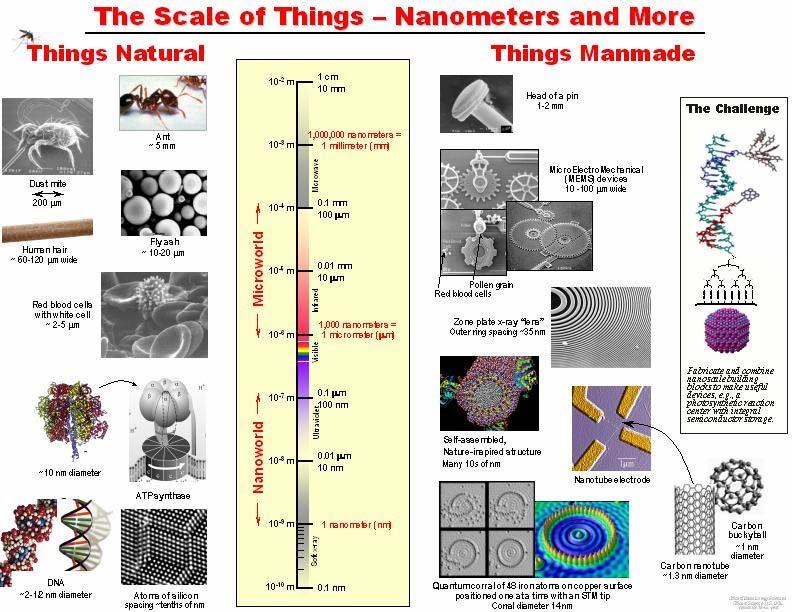
3

4 The scale of things Q. If your hair were 1 km wide (and recall that is ~100 μm), then how large would 1 nanometer (nm) be? To help with your estimate: 1 Km is about the distance from Rte. 65 to River Falls Golf Course or From Main to 6 th St. A. 1 cm!

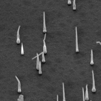
5 A Silica NW ~50 nm Diam. The Hair microns
6 "Nanotechnology has given us the tools...to play with the ultimate toy box of nature -- atoms and molecules. Everything is made from it...the possibilities to create new things appear limitless..." Horst Stormer, Nobel Laureate Columbia University Lucent Technologies
7 Building Nanostructures Top Down Construction: making large things smaller Bottom Up Construction: building things from atoms and molecules
8 Using Atoms and Molecules to Build -- STM Images from Almaden Iron on Copper Xenon on Nickel Iron on Copper
9 Common Nanostructures our building blocks! Chemically Synthesized Quantum Dots Self-assembled Quantum Dots Carbon Nanotubes Semiconducting Nanowires & Nanosheets Other self-assembled molecules

10 Lawrence Livermore Lab


11 Quantum Dots all shapes drexler3.jpg and sizes nppp.ipl.nasa.gov/topics/ Top.quant.dot.htm The University of Melbourne Bawendi, MIT


12 Carbon Nanotubes CNTs: SEM Images CNT Geometry

13 And the ever famous: Nanowires & Nanosheets! All pictures of NWs are from ANU and all Nanosheets from KIST
14 Nanotechnology Begins to Take Its Place The National Nanotechnology Initiative (NNI) is an extraordinarily important investment in the future strength of America's economy, industrial base, and scientific leadership. Recent scientific and technical advances have made it possible to assemble materials and components atom by atom, or molecule by molecule. We are just beginning to understand how to use nanotechnology to build devices and machines that imitate the elegance and economy of nature. Charles M. Vest President Massachusetts Institute of Technology
15 Nanotechnology is indeed here, there, and everywhere: In the clothes you wear In the makeup you use In the car you drive And, coming soon to medicines and medical procedures that help to cure you
16 My particular interest is in: Understanding the physics of NWs Applying this knowledge to make NW-based sensors and devices
17 Nanowire Growth Vapor Liquid Solid Or VLS Method Solid / Liquid Interface Si (111) substrate Begin with Gold Nanosphere Melt Gold Melted Gold Droplet s Diameter NW Diameter Introduce NW material NW material enters Gold & forms eutectic NW grows below Gold as solid forms beneath
B substrate structures: T g <")

18 Different Growth Conditions are responsible for different NW GaAs (111)B substrate structures: T g < 390 C Irregular orientation Kinked substrate 1 μm 390 C T g > 410 C Straight, [111]B aligned Tapered substrate 1 μm 450 C


19 TEM pictures of GaAs NW internal structure Original procedure 450 C 100 nm 400 nm Two-temperature procedure T n = 450 C, T g = 390 C 500 nm 100 nm 100 nm twins Twin defects Facetted sidewalls No planar defects Smooth sidewalls


20 NWs can also be grown into interesting nanostructures. Core-shell Structure NanoTUBE! Axial Differential Growth Quantum Well in NW!


21 III-V Nanowires SEM images 1 μm InAs NWs 1 μm GaP NWs 1 μm AlAs NWs 1 μm GaAs NWs 1 μm AlGaAs NWs


22 II-VI CdS Nanosheets Grown by pulsed laser deposition using vapor-phase transport method with gold catalysts (800 o C; 20min) Dimensions: ~50 nm thick; ~ 4 µm wide & µm long SEM images of ensemble and single nanosheets
23 Slit confocal spectroscopy NW Characterization (some physics!)

24 A series of spectra in 2 InP NWs as Temperature increases. zincblende wurtzite

25 InP NW Photoluminescence Spectra over Time
26 NOW. Onto NW Devices and BioSensors!!

27 NW of Different Materials as PhotoEmitters From: H. Jackson, UC


28 NW LEDs and Lasers From: H. Jackson, UC
29 Nanowires are also finding use in: Filters air and water a woven filter of NWs can filter out ultra-small particles Stronger materials that are still flexible for police and armed forces protection Latest report: for making electricity on a small scale! And of course, in my area of interest


30 Other NW Applications include: NW Solar Cell NW Electricity NanoFiber Mop

31 Nanowires as Biosensors! From: H. Jackson, UC
32 Nanowire BioSensor Schematic Nanowire Sensor Bowtie Resonator Dressed Bowtie Bowtie with Toxins electrodes nanowire I High sensitivity ~10 4 Enhancement at resonance Ligands added Toxins captured, surface plasmon resonance changed

33 Bowtie Plasmonic Resonators


34 First Device Structure: CdS Nanosheet w/ Electrodes Current vs. Voltage
35 Imagine a biosensor array?! A different chemical species detected on each biosensor!
36 Conclusion "The National Nanotechnology Initiative is a big step in a vitally important direction. It will send a clear signal to the youth of this country that the hard core of physical science (particularly physics and chemistry) and the nanofrontiers of engineering have a rich, rewarding future of great social relevance. The coming high tech of building practical things at the ultimate level of finesse, precise right down to the last atom, has the potential to transform our lives. Physics and chemistry are the principal disciplines that will make this all happen. But they are hard disciplines to master, and far too few have perceived the rewards at the end of the road sufficient to justify the effort. The proposed NNI will help immensely to inspire our youth. Richard E. Smalley Gene and Norman Hackerman Professor of Chemistry and Professor of Physics Rice University Center for Nanoscale Science and Technology
37 Thanks to my collaborators at Miami: Graduate Students : Neil Smith, Senthil Rajagopal, Siwei Cao, & Erich See Undergraduate Students: Katie Beddow, Jesse Manders, Colin Boyle, & Caroline Scacca Colleagues at University of Cincinnati: Graduate Students Melodie Fickenscher Faculty Leigh Smith T.B. Hoang S. Perenga Howard Jackson Ashu Mishra Thanks to Synthesis Colleagues: Chenupati Jagadish s Group: Australian National University Collegues: KIST (Korean Institute of Science & Technology Thanks to NSF & DOE for their support


38 JYR 2008 Nano Group Caroline Scacca Jesse Manders Colin Boyle Siwei Cao


39 Grad Students Erich See Siwei Cao


40 Colin Boyle Off to Australia Jesse Manders Off to NIST
41
 University of")
42 Uses for QDs Include: InP QD Laser (where QDs grow on surfaces) University of Stutgart

43 Applications of Nanoscience: Medicine Drug Delivery TEM image of the hexagonallytemplated hollow ZnS on Silica Spheres braungroup.beckman.uiuc.edu/dongyeon.html
 chemistry.st-and.ac.uk/staffmember.")
44 Bottom Up Approach Self Assembly Self-assembled monolayers (SAM) chemistry.st-and.ac.uk/staffmember.php?id=mb
, written with STM into a layer of self assembled molecules. www.nano.geo.uni-muenchen.de/.../molecwrite.")
45 Self-Assembly & STM Note: STM means Scanning Tunneling Microscope Molecular NanoMan logo (line thickness 1-3 nm), written with STM into a layer of self assembled molecules.


46 Spherical QDs with Molecular Tethers form Building Blocks for Sensors
47 CNTs Uses: Similar to nanowires for nanoscale electronics As a strengthener in polymers and other materials As a probe -- in sensors QuickTime and a TIFF (LZW) decompressor are needed to see this picture. Sensor design to left To right, CNTs grown in sensor gap, then used to detect temperature QuickTime and a TIFF (LZW) decompressor are needed to see this picture. IEEE Trans Nanotech, Jan. 2007
48 CdS Nanowires SEM Image AFM Images CdS nanowires grown with 50 nm Au catalysts 14 mm long 17 mm long

49 STM Scanning tunneling microscope
50 Other cool sites (Interesting STM images) roscopes/scanning/ (Interesting STM images)

51 Atomic Force Microscopy


 normal tip (3 µm tall); (b) supertip; (c)")
 Electron micrographs by Jean-Paul Revel,")
52 Wafer & TIP Si or SiN 10 nm at end ~100 atoms Electron micrograph of two 100 µm long V-shaped cantilevers (by Jean-Paul Revel, Caltech; cantilevers from Park Scientific Instruments, Sunnyvale, CA). Three common types of AFM tip. (a) normal tip (3 µm tall); (b) supertip; (c) Ultralever (also 3 µm tall). (b) Electron micrographs by Jean-Paul Revel, Caltech.

53 Non-Contact Mode Solid Lipid Nanoparticles

54 Top-Down Approach: Electronbeam or Optical Lithography Exposure and development process to fabricate a nanoscale structure

55 Incorporating Electrodes into a Device Gold squares are 300 mm and electrodes are in between them! When epoxy is added, then we can add the molecules and the experiment begins.


56 Electrodes for Single Molecules Step 2: Grown shut for 3 nm gap 1 2a Step 1: Fabricated with lithography 2b
57 The bottom up approach holds the most promise: Types of nanoscale building blocks: Quantum Dots - QDs Nanowires - NWs Carbon Nanotubes - CNTs Nanosheets - NSs


58 QDs come in all shapes and sizes! nppp.ipl.nasa.gov/topics/ Top.quant.dot.htm drexler3.jpg gif/qdotspbse.jpg qt.tn.tudelft.nl/news/ NN6fig1b.gif

59 Looking at & Manipulating Atoms STMs & AFMs
29: Nanotechnology. What is Nanotechnology? Properties Control and Understanding. Nanomaterials
 29: Nanotechnology What is Nanotechnology? Properties Control and Understanding Nanomaterials Making nanomaterials Seeing at the nanoscale Quantum Dots Carbon Nanotubes Biology at the Nanoscale Some Applications
Subject Index. See https://pubs.acs.org/sharingguidelines for options on how to legitimately share published articles.
 Subject Index Downloaded via 148.251.232.83 on July 22, 2018 at 01:11:58 (UTC). See https://pubs.acs.org/sharingguidelines for options on how to legitimately share published articles. A American Chemical
Fabrication at the nanoscale for nanophotonics
 Fabrication at the nanoscale for nanophotonics Ilya Sychugov, KTH Materials Physics, Kista silicon nanocrystal by electron beam induced deposition lithography Outline of basic nanofabrication methods Devices
Nanotechnology. Gavin Lawes Department of Physics and Astronomy
 Nanotechnology Gavin Lawes Department of Physics and Astronomy Earth-Moon distance 4x10 8 m (courtesy NASA) Length scales (Part I) Person 2m Magnetic nanoparticle 5x10⁻⁹ m 10 10 m 10 5 m 1 m 10-5 m 10-10
From nanophysics research labs to cell phones. Dr. András Halbritter Department of Physics associate professor
 From nanophysics research labs to cell phones Dr. András Halbritter Department of Physics associate professor Curriculum Vitae Birth: 1976. High-school graduation: 1994. Master degree: 1999. PhD: 2003.
In the name of Allah
 In the name of Allah Nano chemistry- 4 th stage Lecture No. 1 History of nanotechnology 16-10-2016 Assistance prof. Dr. Luma Majeed Ahmed lumamajeed2013@gmail.com, luma.ahmed@uokerbala.edu.iq Nano chemistry-4
Like space travel and the Internet before it, the possibilities of the nano world catches the imagination of school children and scientists alike.
 The Nano World Preface Nano is the cool thing and it s the buzzword Like space travel and the Internet before it, the possibilities of the nano world catches the imagination of school children and scientists
Final Reading Assignment: Travels to the Nanoworld: pages pages pages
 Final Reading Assignment: Travels to the Nanoworld: pages 152-164 pages 201-214 pages 219-227 Bottom-up nanofabrication Can we assemble nanomachines manually? What are the components (parts)? nanoparticles
Nanotechnology. Yung Liou P601 Institute of Physics Academia Sinica
 Nanotechnology Yung Liou P601 yung@phys.sinica.edu.tw Institute of Physics Academia Sinica 1 1st week Definition of Nanotechnology The Interagency Subcommittee on Nanoscale Science, Engineering and Technology
Nanotechnology Fabrication Methods.
 Nanotechnology Fabrication Methods. 10 / 05 / 2016 1 Summary: 1.Introduction to Nanotechnology:...3 2.Nanotechnology Fabrication Methods:...5 2.1.Top-down Methods:...7 2.2.Bottom-up Methods:...16 3.Conclusions:...19
Kavli Workshop for Journalists. June 13th, CNF Cleanroom Activities
 Kavli Workshop for Journalists June 13th, 2007 CNF Cleanroom Activities Seeing nm-sized Objects with an SEM Lab experience: Scanning Electron Microscopy Equipment: Zeiss Supra 55VP Scanning electron microscopes
Nanotechnology is an ever expanding field with improved growth every year.
 What is Nanotechnology? Nanotechnology is the ability to manipulate and modify material properties at the molecular or nanoscale. The ability to modify material properties at the molecular level allows
Materials. Definitions of nanotechnology. The term nanotechnology was invented by Professor Norio Taniguchi at the University of Tokyo in 1971.
 Materials Definitions of nanotechnology The term nanotechnology was invented by Professor Norio Taniguchi at the University of Tokyo in 1971. The original definition, translated into English Nano-technology'
Chapter 10. Nanometrology. Oxford University Press All rights reserved.
 Chapter 10 Nanometrology Oxford University Press 2013. All rights reserved. 1 Introduction Nanometrology is the science of measurement at the nanoscale level. Figure illustrates where nanoscale stands
Seminars in Nanosystems - I
 Seminars in Nanosystems - I Winter Semester 2011/2012 Dr. Emanuela Margapoti Emanuela.Margapoti@wsi.tum.de Dr. Gregor Koblmüller Gregor.Koblmueller@wsi.tum.de Seminar Room at ZNN 1 floor Topics of the
Novel materials and nanostructures for advanced optoelectronics
 Novel materials and nanostructures for advanced optoelectronics Q. Zhuang, P. Carrington, M. Hayne, A Krier Physics Department, Lancaster University, UK u Brief introduction to Outline Lancaster University
State of São Paulo. Brasil. Localization. Santo André
 Brasil State of São Paulo Localization Santo André The Group www.crespilho.com Frank N. Crespilho Pablo R. S. Abdias Group Leader Synthesis of nanostructured materials using polyelectrolytes Andressa R.
III-V nanostructured materials synthesized by MBE droplet epitaxy
 III-V nanostructured materials synthesized by MBE droplet epitaxy E.A. Anyebe 1, C. C. Yu 1, Q. Zhuang 1,*, B. Robinson 1, O Kolosov 1, V. Fal ko 1, R. Young 1, M Hayne 1, A. Sanchez 2, D. Hynes 2, and
Physics and Material Science of Semiconductor Nanostructures
 Physics and Material Science of Semiconductor Nanostructures PHYS 570P Prof. Oana Malis Email: omalis@purdue.edu Course website: http://www.physics.purdue.edu/academic_programs/courses/phys570p/ Lecture
Nanostructure. Materials Growth Characterization Fabrication. More see Waser, chapter 2
 Nanostructure Materials Growth Characterization Fabrication More see Waser, chapter 2 Materials growth - deposition deposition gas solid Physical Vapor Deposition Chemical Vapor Deposition Physical Vapor
Optical Spectroscopies of Thin Films and Interfaces. Dietrich R. T. Zahn Institut für Physik, Technische Universität Chemnitz, Germany
 Optical Spectroscopies of Thin Films and Interfaces Dietrich R. T. Zahn Institut für Physik, Technische Universität Chemnitz, Germany 1. Introduction 2. Vibrational Spectroscopies (Raman and Infrared)
what happens if we make materials smaller?
 what happens if we make materials smaller? IAP VI/10 ummer chool 2007 Couvin Prof. ns outline Introduction making materials smaller? ynthesis how do you make nanomaterials? Properties why would you make
There's Plenty of Room at the Bottom
 There's Plenty of Room at the Bottom 12/29/1959 Feynman asked why not put the entire Encyclopedia Britannica (24 volumes) on a pin head (requires atomic scale recording). He proposed to use electron microscope
Contents. Foreword by Darrell H. Reneker
 Table of Foreword by Darrell H. Reneker Preface page xi xiii 1 Introduction 1 1.1 How big is a nanometer? 1 1.2 What is nanotechnology? 1 1.3 Historical development of nanotechnology 2 1.4 Classification
ESH Benign Processes for he Integration of Quantum Dots (QDs)
") ESH Benign Processes for he Integration of Quantum Dots (QDs) PIs: Karen K. Gleason, Department of Chemical Engineering, MIT Graduate Students: Chia-Hua Lee: PhD Candidate, Department of Material Science
ESH Benign Processes for he Integration of Quantum Dots (QDs) PIs: Karen K. Gleason, Department of Chemical Engineering, MIT Graduate Students: Chia-Hua Lee: PhD Candidate, Department of Material Science
Lecture 3: Heterostructures, Quasielectric Fields, and Quantum Structures
 Lecture 3: Heterostructures, Quasielectric Fields, and Quantum Structures MSE 6001, Semiconductor Materials Lectures Fall 2006 3 Semiconductor Heterostructures A semiconductor crystal made out of more
Physics and Material Science of Semiconductor Nanostructures
 Physics and Material Science of Semiconductor Nanostructures PHYS 570P Prof. Oana Malis Email: omalis@purdue.edu Course website: http://www.physics.purdue.edu/academic_programs/courses/phys570p/ 1 Course
NANOSCIENCE: TECHNOLOGY AND ADVANCED MATERIALS
 UNIVERSITY OF SOUTHAMPTON PHYS6014W1 SEMESTER 2 EXAMINATIONS 2012-2013 NANOSCIENCE: TECHNOLOGY AND ADVANCED MATERIALS DURATION 120 MINS (2 Hours) This paper contains 8 questions Answer ALL questions in
Semiconductor Nanowires: Motivation
 Semiconductor Nanowires: Motivation Patterning into sub 50 nm range is difficult with optical lithography. Self-organized growth of nanowires enables 2D confinement of carriers with large splitting of
Lesson 4: Tools of the Nanosciences. Student Materials
 Lesson 4: Tools of the Nanosciences Student Materials Contents Black Box Lab Activity: Student Instructions and Worksheet Seeing and Building Small Things: Student Reading Seeing and Building Small Things:
There s plenty of room at the bottom! - R.P. Feynman, Nanostructure: a piece of material with at least one dimension less than 100 nm in extent.
 Nanostructures and Nanotechnology There s plenty of room at the bottom! - R.P. Feynman, 1959 Materials behave differently when structured at the nm scale than they do in bulk. Technologies now exist that
Scanning Probe Microscopy. Amanda MacMillan, Emmy Gebremichael, & John Shamblin Chem 243: Instrumental Analysis Dr. Robert Corn March 10, 2010
 Scanning Probe Microscopy Amanda MacMillan, Emmy Gebremichael, & John Shamblin Chem 243: Instrumental Analysis Dr. Robert Corn March 10, 2010 Scanning Probe Microscopy High-Resolution Surface Analysis
Chapter 12. Nanometrology. Oxford University Press All rights reserved.
 Chapter 12 Nanometrology Introduction Nanometrology is the science of measurement at the nanoscale level. Figure illustrates where nanoscale stands in relation to a meter and sub divisions of meter. Nanometrology
Imaging Methods: Scanning Force Microscopy (SFM / AFM)
") Imaging Methods: Scanning Force Microscopy (SFM / AFM) The atomic force microscope (AFM) probes the surface of a sample with a sharp tip, a couple of microns long and often less than 100 Å in diameter.
Imaging Methods: Scanning Force Microscopy (SFM / AFM) The atomic force microscope (AFM) probes the surface of a sample with a sharp tip, a couple of microns long and often less than 100 Å in diameter.
Nano-mechatronics. Presented by: György BudaváriSzabó (X0LY4M)
") Nano-mechatronics Presented by: György BudaváriSzabó (X0LY4M) Nano-mechatronics Nano-mechatronics is currently used in broader spectra, ranging from basic applications in robotics, actuators, sensors,
Nano-mechatronics Presented by: György BudaváriSzabó (X0LY4M) Nano-mechatronics Nano-mechatronics is currently used in broader spectra, ranging from basic applications in robotics, actuators, sensors,
Nanotechnology? Source: National Science Foundation (NSF), USA
, USA") 2 2 Nanotechnology? Ability to work at the atomic, molecular and even sub-molecular levels in order to create and use material structures, devices and systems with new properties and functions Source:
2 2 Nanotechnology? Ability to work at the atomic, molecular and even sub-molecular levels in order to create and use material structures, devices and systems with new properties and functions Source:
Electrochemically Synthesized Multi-block
 Electrochemically Synthesized Multi-block Nanorods Sungho Park SungKyunKwan University, Department of Chemistry & SKKU Advanced Institute of Nanotechnology (SAINT) J. Am. Chem. Soc. 2003, 125, 2282-2290
672 Advanced Solid State Physics. Scanning Tunneling Microscopy
 672 Advanced Solid State Physics Scanning Tunneling Microscopy Biao Hu Outline: 1. Introduction to STM 2. STM principle & working modes 3. STM application & extension 4. STM in our group 1. Introduction
High-resolution Characterization of Organic Ultrathin Films Using Atomic Force Microscopy
 High-resolution Characterization of Organic Ultrathin Films Using Atomic Force Microscopy Jing-jiang Yu Nanotechnology Measurements Division Agilent Technologies, Inc. Atomic Force Microscopy High-Resolution
QUANTUM NANOSTRUCTURES
 QUANTUM NANOSTRUCTURES by Droplet Epitaxy Somsak Panyakeow Semiconductor Device Research Laboratory (SDRL), CoE Nanotechnology Center of Thailand, Department of Electrical Engineering, Faculty of Engineering,
I. NANOFABRICATION O AND CHARACTERIZATION Chap. 2 : Self-Assembly
 I. Nanofabrication and Characterization : TOC I. NANOFABRICATION O AND CHARACTERIZATION Chap. 1 : Nanolithography Chap. 2 : Self-Assembly Chap. 3 : Scanning Probe Microscopy Nanoscale fabrication requirements
D DAVID PUBLISHING. Study the Synthesis Parameter of Tin Oxide Nanostructure. 1. Introduction. 2. Experiment
 Journal of Materials Science and Engineering B 5 (9-10) (2015) 353-360 doi: 10.17265/2161-6221/2015.9-10.003 D DAVID PUBLISHING Study the Synthesis Parameter of Tin Oxide Nanostructure Gyanendra Prakash
Nanolithography Techniques
 Nanolithography Techniques MSE 505 / MSNT 505 P. Coane Outline What Is Nanotechnology? The Motivation For Going Small Nanofabrication Technologies Basic Techniques Nano Lithography NANOTECHNOLOGY Nanotechnology
CSCI 2570 Introduction to Nanocomputing
 CSCI 2570 Introduction to Nanocomputing The Emergence of Nanotechnology John E Savage Purpose of the Course The end of Moore s Law is in sight. Researchers are now exploring replacements for standard methods
The first three categories are considered a bottom-up approach while lithography is a topdown
 Nanowires and Nanorods One-dimensional structures have been called in different ways: nanowires, nanorod, fibers of fibrils, whiskers, etc. The common characteristic of these structures is that all they
1.1. Introduction to Nanoscience and Nanotechnology
 1.1. Introduction to Nanoscience and Nanotechnology 1.1.1. A Brief Historical Overview Before trying to understand and discuss about synthesis, characterization and application of nanomaterials, it is
Techniken der Oberflächenphysik (Technique of Surface Physics)
") Techniken der Oberflächenphysik (Technique of Surface Physics) Yong Lei & Fabian Grote Fachgebiet 3D-Nanostrukturierung, Institut für Physik Contact: yong.lei@tu-ilmenau.de; fabian.grote@tu-ilmenau.de
Techniken der Oberflächenphysik (Technique of Surface Physics) Yong Lei & Fabian Grote Fachgebiet 3D-Nanostrukturierung, Institut für Physik Contact: yong.lei@tu-ilmenau.de; fabian.grote@tu-ilmenau.de
An Introduction to NanoScience and NanoTechnology
 An Introduction to NanoScience and NanoTechnology ELEC 6271/498X An Overview Introduction Evolution of IC characteristics in order of magnitude from the time that the technology was introduced in 1960:
PERIODIC ARRAYS OF METAL NANOBOWLS AS SERS-ACTIVE SUBSTRATES
 PERIODIC ARRAYS OF METAL NANOBOWLS AS SERS-ACTIVE SUBSTRATES Lucie ŠTOLCOVÁ a, Jan PROŠKA a, Filip NOVOTNÝ a, Marek PROCHÁZKA b, Ivan RICHTER a a Czech Technical University in Prague, Faculty of Nuclear
Nano-optics. Topics: How do we image things on the nanoscale? How do we use nanofabrication for new optical devices? COSMOS 2006 Lecture 1
 Nano-optics Topics: How do we image things on the nanoscale? How do we use nanofabrication for new optical devices? Wave Optics 1. Electromagnetic wave x Ex λ Direction of Propagation y z z plane wave
PH575 Spring Lecture #28 Nanoscience: the case study of graphene and carbon nanotubes.
 PH575 Spring 2014 Lecture #28 Nanoscience: the case study of graphene and carbon nanotubes. Nanoscience scale 1-100 nm "Artificial atoms" Small size => discrete states Large surface to volume ratio Bottom-up
1. Nanotechnology & nanomaterials -- Functional nanomaterials enabled by nanotechnologies.
 Novel Nano-Engineered Semiconductors for Possible Photon Sources and Detectors NAI-CHANG YEH Department of Physics, California Institute of Technology 1. Nanotechnology & nanomaterials -- Functional nanomaterials
Nanosphere Lithography
 Nanosphere Lithography Derec Ciafre 1, Lingyun Miao 2, and Keita Oka 1 1 Institute of Optics / 2 ECE Dept. University of Rochester Abstract Nanosphere Lithography is quickly emerging as an efficient, low
Introduction to Nanotechnology Chapter 5 Carbon Nanostructures Lecture 1
 Introduction to Nanotechnology Chapter 5 Carbon Nanostructures Lecture 1 ChiiDong Chen Institute of Physics, Academia Sinica chiidong@phys.sinica.edu.tw 02 27896766 Carbon contains 6 electrons: (1s) 2,
Electrical and Optical Properties. H.Hofmann
 Introduction to Nanomaterials Electrical and Optical Properties H.Hofmann Electrical Properties Ohm: G= σw/l where is the length of the conductor, measured in meters [m], A is the cross-section area of
Course file PPY15204 Nanoscience and Nanomaterials Table of Contents
 Department Physics Nanotechnology : M.sc Physics Course file PPY15204 Table Contents Second Year MSc Physics (2015-2016 Regulation) Detailed Lesson Plan UNIT-I: INTRODUCTION TO NANOTECHNOLOGY History Importance
Other SPM Techniques. Scanning Probe Microscopy HT10
 Other SPM Techniques Scanning Near-Field Optical Microscopy (SNOM) Scanning Capacitance Microscopy (SCM) Scanning Spreading Resistance Microscopy (SSRM) Multiprobe techniques Electrostatic Force Microscopy,
In today s lecture, we will cover:
 In today s lecture, we will cover: Metal and Metal oxide Nanoparticles Semiconductor Nanocrystals Carbon Nanotubes 1 Week 2: Nanoparticles Goals for this section Develop an understanding of the physical
ME 4875/MTE C16. Introduction to Nanomaterials and Nanotechnology. Lecture 2 - Applications of Nanomaterials + Projects
 ME 4875/MTE 575 - C16 Introduction to Nanomaterials and Nanotechnology Lecture 2 - Applications of Nanomaterials + Projects 1 Project Teams of 4 students each Literature review of one application of nanotechnology
Nano Materials and Devices
 Nano Materials and Devices Professor Michael Austin Platform Technologies Research Institute Nano Materials and Devices Program Aim: to develop an integrated capability in nanotechnology Design and modelling
NANONICS IMAGING FOUNTAIN PEN
 NANONICS IMAGING FOUNTAIN PEN NanoLithography Systems Methods of Nanochemical Lithography Fountain Pen NanoLithography A. Lewis et al. Appl. Phys. Lett. 75, 2689 (1999) FPN controlled etching of chrome.
Ultrafast single photon emitting quantum photonic structures. based on a nano-obelisk
 Ultrafast single photon emitting quantum photonic structures based on a nano-obelisk Je-Hyung Kim, Young-Ho Ko, Su-Hyun Gong, Suk-Min Ko, Yong-Hoon Cho Department of Physics, Graduate School of Nanoscience
Strong Coupling between On Chip Notched Ring Resonator and Nanoparticle
 Strong Coupling between On Chip Notched Ring Resonator and Nanoparticle S. Wang 1, K. Broderick 1, 3, H. Smith 1 2, 3,1 *, and Y. Yi 1 Massauchusetts Institute of Technology, Cambridge, MA 02139 2 New
Nanomaterial based Environmental Sensing. Sung Ik Yang Kyung Hee University
 Nanomaterial based Environmental Sensing Sung Ik Yang Kyung Hee University What is Nanotechnology? - understanding and control of matter at dimensions less than 100 nanometers- unique phenomena enable
Enhanced Photonic Properties of Thin Opaline Films as a Consequence of Embedded Nanoparticles.
 Enhanced Photonic Properties of Thin Opaline Films as a Consequence of Embedded Nanoparticles. D E Whitehead, M Bardosova and M E Pemble Tyndall National Institute, University College Cork Ireland Introduction:
Lesson 1: Introduction to Nanoscience. Teacher Materials
 Lesson 1: Introduction to Nanoscience Teacher Materials Contents Introduction to Nanoscience: Teacher Lesson Plan Introduction to Nanoscience: PowerPoint with Teacher Notes Introduction to Nanoscience
Large-Area and Uniform Surface-Enhanced Raman. Saturation
 Supporting Information Large-Area and Uniform Surface-Enhanced Raman Spectroscopy Substrate Optimized by Enhancement Saturation Daejong Yang 1, Hyunjun Cho 2, Sukmo Koo 1, Sagar R. Vaidyanathan 2, Kelly
MSN551 LITHOGRAPHY II
 MSN551 Introduction to Micro and Nano Fabrication LITHOGRAPHY II E-Beam, Focused Ion Beam and Soft Lithography Why need electron beam lithography? Smaller features are required By electronics industry:
Nanotechnology where size matters
 Nanotechnology where size matters J Emyr Macdonald Overview Ways of seeing very small things What is nanotechnology and why is it important? Building nanostructures What we can do with nanotechnology?
Nanophysics: Main trends
 Nano-opto-electronics Nanophysics: Main trends Nanomechanics Main issues Light interaction with small structures Molecules Nanoparticles (semiconductor and metallic) Microparticles Photonic crystals Nanoplasmonics
Chapter 1 Introduction
 Chapter 1 Introduction A nanometer (nm) is one billionth (10-9 ) of a meter. Nanoscience can be defined as the science of objects and phenomena occurring at the scale of 1 to 100 nm. The range of 1 100
Interdisciplinary Nanoscience Center University of Aarhus, Denmark. Design and Imaging. Assistant Professor.
 Interdisciplinary Nanoscience Center University of Aarhus, Denmark Design and Imaging DNA Nanostructures Assistant Professor Wael Mamdouh wael@inano.dk Molecular Self-assembly Synthesis, SPM microscopy,
Fabrication / Synthesis Techniques
 Quantum Dots Physical properties Fabrication / Synthesis Techniques Applications Handbook of Nanoscience, Engineering, and Technology Ch.13.3 L. Kouwenhoven and C. Marcus, Physics World, June 1998, p.35
Nanostrukturphysik (Nanostructure Physics)
") Nanostrukturphysik (Nanostructure Physics) Prof. Yong Lei & Dr. Yang Xu Fachgebiet 3D-Nanostrukturierung, Institut für Physik Contact: yong.lei@tu-ilmenau.de; yang.xu@tu-ilmenau.de Office: Unterpoerlitzer
Nanostrukturphysik (Nanostructure Physics) Prof. Yong Lei & Dr. Yang Xu Fachgebiet 3D-Nanostrukturierung, Institut für Physik Contact: yong.lei@tu-ilmenau.de; yang.xu@tu-ilmenau.de Office: Unterpoerlitzer
Printing Silver Nanogrids on Glass: A Hands-on Investigation of Transparent Conductive Electrodes
 Printing Silver Nanogrids on Glass: A Hands-on Investigation of Transparent Conductive Electrodes Silver Nanogrid/Nanowire Importance The next generation of optoelectronic devices requires transparent
Fabrication of ordered array at a nanoscopic level: context
 Fabrication of ordered array at a nanoscopic level: context Top-down method Bottom-up method Classical lithography techniques Fast processes Size limitations it ti E-beam techniques Small sizes Slow processes
Mercury(II) detection by SERS based on a single gold microshell
 detection by SERS based on a single gold microshell") Mercury(II) detection by SERS based on a single gold microshell D. Han, S. Y. Lim, B. J. Kim, L. Piao and T. D. Chung* Department of Chemistry, Seoul National University, Seoul, Korea. 2010, 46, 5587-558
Mercury(II) detection by SERS based on a single gold microshell D. Han, S. Y. Lim, B. J. Kim, L. Piao and T. D. Chung* Department of Chemistry, Seoul National University, Seoul, Korea. 2010, 46, 5587-558
Semiconductor Nanowires. Stefan Heun NEST, Istituto Nanoscienze-CNR and Scuola Normale Superiore, Pisa, Italy
 Semiconductor Nanowires Stefan Heun NEST, Istituto Nanoscienze-CNR and Scuola Normale Superiore, Pisa, Italy Leaning Tower in Pisa Pisa and Hangzhou: Twin towns since 2008 Institute of Nanoscience- National
Introduction to Nanoscience and Nanotechnology
 Introduction to Nanoscience and Nanotechnology ENS 463 by Alexander M. Zaitsev alexander.zaitsev@csi.cuny.edu Tel: 718 982 2812 Office 4N101b 1 What is the size for a nano? 10-3 m, (milli) Macroobjects,
Unconventional Nano-patterning. Peilin Chen
 Unconventional Nano-patterning Peilin Chen Reference Outlines History of patterning Traditional Nano-patterning Unconventional Nano-patterning Ancient Patterning "This is the Elks' land". A greeting at
Nanotechnology Nanofabrication of Functional Materials. Marin Alexe Max Planck Institute of Microstructure Physics, Halle - Germany
 Nanotechnology Nanofabrication of Functional Materials Marin Alexe Max Planck Institute of Microstructure Physics, Halle - Germany Contents Part I History and background to nanotechnology Nanoworld Nanoelectronics
Multiple-Patterning Nanosphere Lithography for Fabricating Periodic Three-Dimensional Hierarchical Nanostructures
 Supporting Information Multiple-Patterning Nanosphere Lithography for Fabricating Periodic Three-Dimensional Hierarchical Nanostructures Xiaobin Xu, 1,2 Qing Yang, 1,2 Natcha Wattanatorn, 1,2 Chuanzhen
National Science and Technology Council (NSTC) Committee on Technology
 Committee on Technology") BY LYNN YARRIS "The emerging fields of nanoscience and nanoengineering are leading to unprecedented understanding and control over the fundamental building blocks of all physical things. This is likely
BY LYNN YARRIS "The emerging fields of nanoscience and nanoengineering are leading to unprecedented understanding and control over the fundamental building blocks of all physical things. This is likely
Nanostructures Fabrication Methods
 Nanostructures Fabrication Methods bottom-up methods ( atom by atom ) In the bottom-up approach, atoms, molecules and even nanoparticles themselves can be used as the building blocks for the creation of
Self-Assembled InAs Quantum Dots on Patterned InP Substrates
 Self-Assembled InAs Quantum Dots on Patterned InP Substrates J. Lefebvre, P.J. Poole, J. Fraser, G.C. Aers, D. Chithrani, and R.L. Williams Institute for Microstructural Sciences, National Research Council
City University of Hong Kong. Course Syllabus. offered by Department of Physics and Materials Science with effect from Semester A 2016 / 17
 City University of Hong Kong offered by Department of Physics and Materials Science with effect from Semester A 2016 / 17 Part I Course Overview Course Title: Nanostructures and Nanotechnology Course Code:
Electrochemical Deposition of Iron Nanoparticles on PPY and H terminated Si substrates. Karan Sukhija Co-op Term # 1 April 28 th, 2005
 Electrochemical Deposition of Iron Nanoparticles on PPY and H terminated Si substrates Karan Sukhija Co-op Term # 1 April 28 th, 2005 Future Suggested Experiments Acknowledgments Presentation Outline Background
And Manipulation by Scanning Probe Microscope
 Basic 15 Nanometer Scale Measurement And Manipulation by Scanning Probe Microscope Prof. K. Fukuzawa Dept. of Micro/Nano Systems Engineering Nagoya University I. Basics of scanning probe microscope Basic
NANOSCIENCE AND NANOTECHNOLOGY
 NANOSCIENCE AND NANOTECHNOLOGY Yuehe Lin WHAT IS NANOTECHNOLOGY Nanotechnology is the understanding and control of matter at dimensions of roughly 1 to 100 nanometers, where unique phenomena enable novel
Carbon based Nanoscale Electronics
 Carbon based Nanoscale Electronics 09 02 200802 2008 ME class Outline driving force for the carbon nanomaterial electronic properties of fullerene exploration of electronic carbon nanotube gold rush of
Graphene Fundamentals and Emergent Applications
 Graphene Fundamentals and Emergent Applications Jamie H. Warner Department of Materials University of Oxford Oxford, UK Franziska Schaffel Department of Materials University of Oxford Oxford, UK Alicja
NANOTECHNOLOGY. Students will gain an understanding of nanoscale dimensions and nanotechnology.
 NANOTECHNOLOGY By Anna M. Waldron and Carl A. Batt, Nanobiotechnology Center, Cornell University Subjects: Nanotechnology, Chemistry, Physics Time: Two class periods (approximately 90 minutes) Objective:
ALIGNED CARBON NANOTUBES FOR MULTIFUNCTIONAL NANOCOMPOSITES AND NANODEVICES:
 ALIGNED CARBON NANOTUBES FOR MULTIFUNCTIONAL NANOCOMPOSITES AND NANODEVICES: Multicomponent Micropatterned Aligned Carbon Nanotube Devices with Reversibly Switchable Electronic Properties for Multifunctional
Nanotechnology: Today and tomorrow
 Nanotechnology: Today and tomorrow Horst-Günter Rubahn NanoSYD Mads Clausen Instituttet Syddansk Universitet Alsion 2 6400 Sønderborg Agenda Alsion A bit about nano Nanoproducts Top down vs. bottom up
Supplementary Figure 1 Detailed illustration on the fabrication process of templatestripped
 Supplementary Figure 1 Detailed illustration on the fabrication process of templatestripped gold substrate. (a) Spin coating of hydrogen silsesquioxane (HSQ) resist onto the silicon substrate with a thickness
Instrumentation and Operation
 Instrumentation and Operation 1 STM Instrumentation COMPONENTS sharp metal tip scanning system and control electronics feedback electronics (keeps tunneling current constant) image processing system data
NTECH - Nanotechnology
 Coordinating unit: Teaching unit: Academic year: Degree: ECTS credits: 2017 230 - ETSETB - Barcelona School of Telecommunications Engineering 710 - EEL - Department of Electronic Engineering 713 - EQ -
NANOMEDICINE. WILEY A John Wiley and Sons, Ltd., Publication DESIGN AND APPLICATIONS OF MAGNETIC NANOMATERIALS, NANOSENSORS AND NANOSYSTEMS
 NANOMEDICINE DESIGN AND APPLICATIONS OF MAGNETIC NANOMATERIALS, NANOSENSORS AND NANOSYSTEMS Vijay K. Varadan Linfeng Chen Jining Xie WILEY A John Wiley and Sons, Ltd., Publication Preface About the Authors
Self-Assembled InAs Quantum Dots
 Self-Assembled InAs Quantum Dots Steve Lyon Department of Electrical Engineering What are semiconductors What are semiconductor quantum dots How do we make (grow) InAs dots What are some of the properties
Top down and bottom up fabrication
 Lecture 24 Top down and bottom up fabrication Lithography ( lithos stone / graphein to write) City of words lithograph h (Vito Acconci, 1999) 1930 s lithography press Photolithography d 2( NA) NA=numerical