Selective Molecular Transport through Intrinsic Defects in a Single Layer of CVD Graphene
|
|
|
- Adela Hardy
- 5 years ago
- Views:
Transcription


1 Selective Molecular Transport through Intrinsic Defects in a Single Layer of CVD Graphene Sean C. O Hern, Cameron A. Stewart, Michael S. H. Boutilier, Juan-Carlos Idrobo, Sreekar Bhaviripudi, Sarit K. Das,^ Jing Kong, Tahar Laoui,# Muataz Atieh,#and Rohit Karnik,* Department of Mechanical Engineering, Massachusetts Institute of Technology, Cambridge, Massachusetts 02139, United States, Materials Science and Technology Division, Oak Ridge National Laboratory, Oak Ridge, Tennessee 37831, United States, Department of Electrical Engineering and Computer Science, Massachusetts Institute of Technology, Cambridge, Massachusetts 02139, United States, ^Department of Mechanical Engineering, Indian Institute of Technology Madras, Chennai, India, and # Departments of Mechanical and Chemical Engineering, King Fahd University of Petroleum and Minerals, Dhahran, Saudi Arabia Soujit Sengupta Date:
2 Introduction Graphene, with its atomistic thickness, remarkable mechanical strength, and potential for size-selective transport through nanometer-scale holes in its lattice, is an ideal material for next generation membranes with high selectivity and permeability. Although impermeable in its pristine state, theoretical models predict that by the introduction of holes of controlled size, density, and functionalization, graphene membranes would outperform existing state-of-the-art membranes in gas-phase and liquid-phase separation processes. Experimental measurements of ionic and molecular transport through graphene membranes have so far been limited to microscopic areas. DNA translocation has been detected via measurement of ionic currents through single nanopores in suspended graphene, while graphene nanoballoon measurements have demonstrated the impermeability of pristine graphene to gases including helium. Much progress is required beyond the current status for exploiting the incredible potential of graphene to realize practical membranes, including advances in methods for fabricating large-area, nearly defect free graphene on porous supports, generating a high density of controlled nanoscale pores, and better understanding of the relationship between the pore structures and transport properties.
3 Introduction Here, they experimentally investigate the transport of ions and molecules across a single layer of large-area CVD graphene transferred to a porous polycarbonate track. They develop a procedure to transfer graphene ( 25 mm 2 ) to the PCTE membrane and characterize the coverage of the transferred graphene using pressure-driven flow. They show that the CVD graphene contains a low frequency of intrinsic holes that permit the selective transport of molecules. The measured permeability is consistent with predictions of continuum theory.
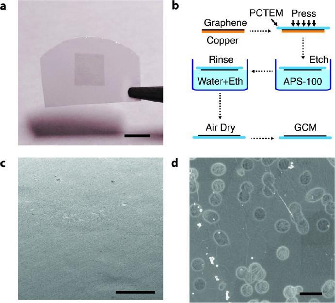
4 Experimental section Membrane fabrication: They used CVD graphene on copper, as it can be grown over large areas comprising primarily single layers. Their scalable, direct-transfer process relies on the conformability of a porous polymer substrate to adhere to the graphene (on copper) via a simple pressing process followed by etching of the copper. The porous polymer supports the graphene during the copper-etching phase and also gives it sufficient mechanical robustness for further handling. Before drying, the GCM was rinsed in an ethanol/water mixture to minimize mechanical stresses due to the receding meniscus.
5
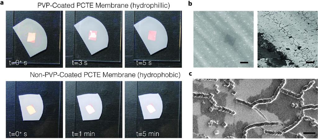
6 They found that the three primary factors that influence the quality of the transfer are the: 1. Hydrophobicity of the substrate, 2. The surface roughness of the copper on which the graphene is grown, and 3. The type of etchant used to remove the copper.
7

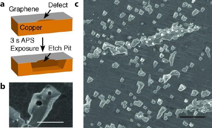
8 Uncovered single polycarbonate track etch membrane pores (indicated by arrows) and cracks (inset) were two types of defects commonly found in graphene after transfer. Analysis of similar images revealed typical graphene coverage to be 90-98%. Scale bars are 500 nm.
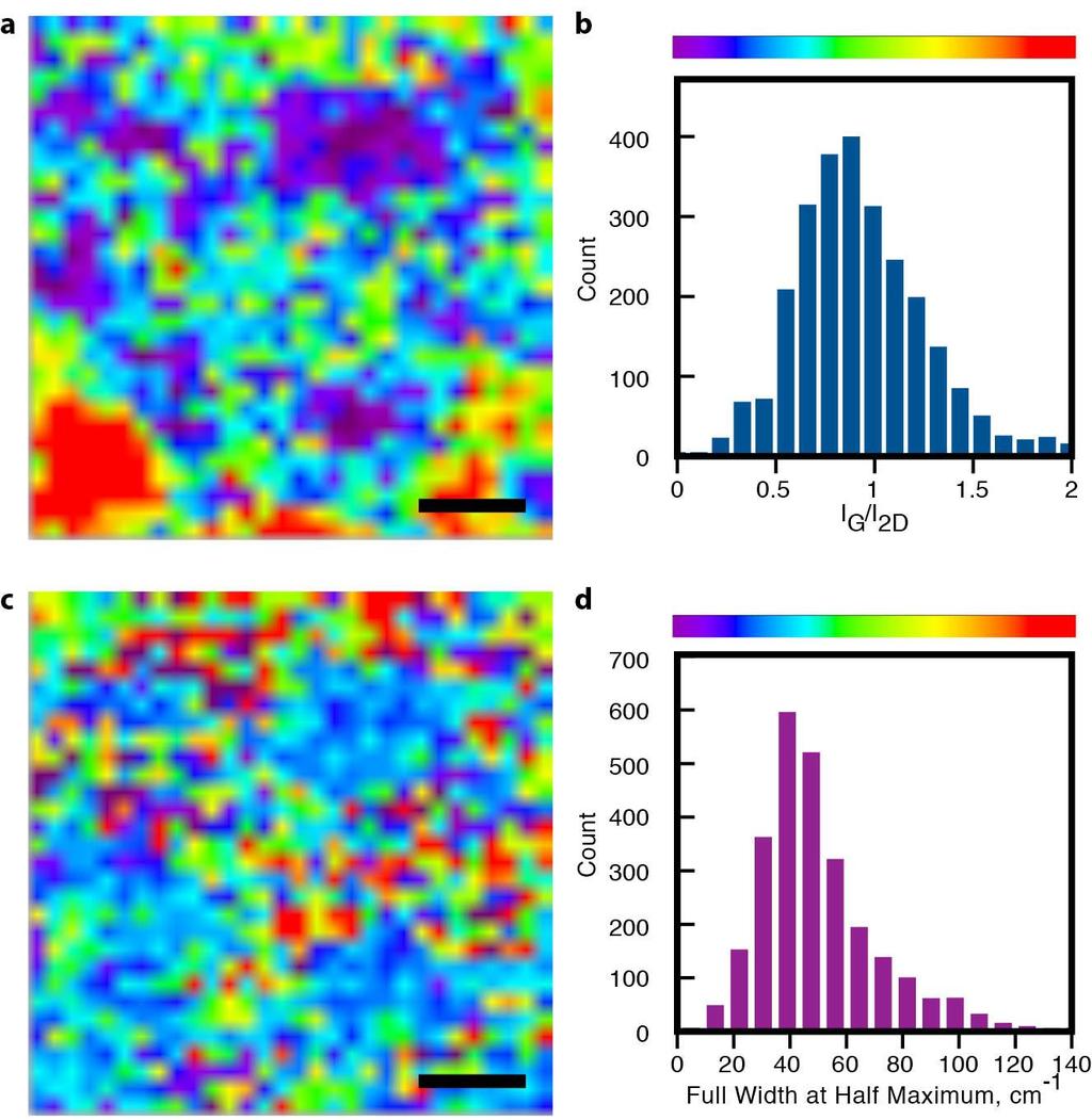
9 Characterization of graphene
10
11
 Representative images of pores that vary in size from 1 to 15 nmin diameter. Scale bars are 2 nm.")
12 Characterization of nanometer-scale pores in graphene by STEM medium-angle annular dark field (MAADF). (a) Low density of pores can be seen in the graphene lattice, as indicated by red arrows. Scale bar is 10 nm. (be) Representative images of pores that vary in size from 1 to 15 nmin diameter. Scale bars are 2 nm. (f) A higher concentration of pores exists in the region between the dashed lines. Scale bar is 1 μm. (g) Distribution of pore sizes imaged in STEM suggests 83% of holes in lattice are less than 10 nm in diameter.
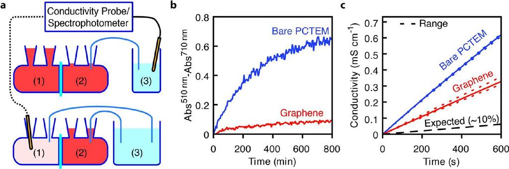
13 a, Raman shift of graphene for APS-100 etch times of 5 min, 30 min, 1.5 h and 24 h. Increasing D-band and D -band suggest APS-100 may modify graphene lattice. b, Diffusive transport rate of KCl through graphene membrane for etch times of 0 h, 17 h, and 91 h. Lack of substantial transport increase suggests that APS-100 does not increase intrinsic hole size.
14
15 Summary and conclusion In this work, they fabricated membranes comprising a single sheet of CVD graphene on a porous support and developed methods to measure the transport properties of graphene. The understanding of the origins of the permeability of graphene and the measurement techniques developed in this study will aid the design of future graphene membranes for various applications and may also provide insights into the behavior of graphene as barrier films. This study shows that these defects occur at a fairly low frequency, and they can only speculate that they occur due to defects in the copper itself or deposition and growth of particulates on the copper. The work promises to reveal interesting transport properties for applications in gas separations, water purification, and biomedicine.


16 Thank you
Separating the components of a gaseous
 Implications of Permeation through Intrinsic Defects in Graphene on the Design of Defect-Tolerant Membranes for Gas Separation Michael S. H. Boutilier, Chengzhen Sun,, Sean C. O Hern, Harold Au, Nicolas
Nanofiltration across Defect-Sealed Nanoporous Monolayer Graphene
 Nanofiltration across Defect-Sealed Nanoporous Monolayer Graphene Sean C. O Hern 1, Doojoon Jang 1, Suman Bose 1, Juan-Carlos Idrobo 2, Yi Song 3, Tahar Laoui 4, Jing Kong 3, and Rohit Karnik 1* 1 Department
Selective Ionic Transport through Tunable Subnanometer Pores in Single-Layer Graphene Membranes
 Selective Ionic Transport through Tunable Subnanometer Pores in Single-Layer Graphene Membranes The MIT Faculty has made this article openly available. Please share how this access benefits you. Your story
A. Optimizing the growth conditions of large-scale graphene films
 1 A. Optimizing the growth conditions of large-scale graphene films Figure S1. Optical microscope images of graphene films transferred on 300 nm SiO 2 /Si substrates. a, Images of the graphene films grown
Toward Clean Suspended CVD Graphene
 Electronic Supplementary Material (ESI) for RSC Advances. This journal is The Royal Society of Chemistry 2016 Supplemental information for Toward Clean Suspended CVD Graphene Alexander Yulaev 1,2,3, Guangjun
Supplementary Figures Supplementary Figure 1
 Supplementary Figures Supplementary Figure 1 Optical images of graphene grains on Cu after Cu oxidation treatment at 200 for 1m 30s. Each sample was synthesized with different H 2 annealing time for (a)
on Self-Assembly of Fullerene Molecules
 Effect of Surface Preparation of Copper on Self-Assembly of Fullerene Molecules Dongni Ma, Selene Sandoval, Krishna Muralidharan, Srini Raghavan University of Arizona Department of Materials Science and
Omnidirectionally Stretchable and Transparent Graphene Electrodes
 Supporting Information for: Omnidirectionally Stretchable and Transparent Graphene Electrodes Jin Yong Hong,, Wook Kim, Dukhyun Choi, Jing Kong,*, and Ho Seok Park*, School of Chemical Engineering, Sungkyunkwan
Engineered Flexible Conductive Barrier Films for Advanced Energy Devices
 The 13 th Korea-U.S. Forum on Nanotechnology Engineered Flexible Conductive Barrier Films for Advanced Energy Devices Jinsung Kwak 1, Yongsu Jo 1, Soon-Dong Park 2, Na Yeon Kim 1, Se-Yang Kim 1, Zonghoon
Supplementary Figure 1 Experimental setup for crystal growth. Schematic drawing of the experimental setup for C 8 -BTBT crystal growth.
 Supplementary Figure 1 Experimental setup for crystal growth. Schematic drawing of the experimental setup for C 8 -BTBT crystal growth. Supplementary Figure 2 AFM study of the C 8 -BTBT crystal growth
Figure 1: Graphene release, transfer and stacking processes. The graphene stacking began with CVD
 Supplementary figure 1 Graphene Growth and Transfer Graphene PMMA FeCl 3 DI water Copper foil CVD growth Back side etch PMMA coating Copper etch in 0.25M FeCl 3 DI water rinse 1 st transfer DI water 1:10
Self-study problems and questions Processing and Device Technology, FFF110/FYSD13
 Self-study problems and questions Processing and Device Technology, FFF110/FYSD13 Version 2016_01 In addition to the problems discussed at the seminars and at the lectures, you can use this set of problems
Supplementary Figure 1: Micromechanical cleavage of graphene on oxygen plasma treated Si/SiO2. Supplementary Figure 2: Comparison of hbn yield.
 1 2 3 4 Supplementary Figure 1: Micromechanical cleavage of graphene on oxygen plasma treated Si/SiO 2. Optical microscopy images of three examples of large single layer graphene flakes cleaved on a single
Observation of Extreme Phase Transition Temperatures of Water Confined Inside Isolated Carbon Nanotubes
 Observation of Extreme Phase Transition Temperatures of Water Confined Inside Isolated Carbon Nanotubes Kumar Varoon Agrawal, Steven Shimizu, Lee W. Drahushuk, Daniel Kilcoyne and Michael S. Strano Department
Graphene: A sub-nanometer trans-electrode membrane
 1 Graphene: A sub-nanometer trans-electrode membrane S. Garaj 1, W. Hubbard 2, A. Reina 3, J. Kong 4, D. Branton 5 & J.A. Golovchenko 1,2* Submitted 12 April 2010 to Nature, where it is under review. 1
Solutions for Assignment-8
 Solutions for Assignment-8 Q1. The process of adding impurities to a pure semiconductor is called: [1] (a) Mixing (b) Doping (c) Diffusing (d) None of the above In semiconductor production, doping intentionally
Intensity (a.u.) Intensity (a.u.) Raman Shift (cm -1 ) Oxygen plasma. 6 cm. 9 cm. 1mm. Single-layer graphene sheet. 10mm. 14 cm
 Intensity (a.u.) Raman Shift (cm -1 ) Oxygen plasma. 6 cm. 9 cm. 1mm. Single-layer graphene sheet. 10mm. 14 cm") Intensity (a.u.) Intensity (a.u.) a Oxygen plasma b 6 cm 1mm 10mm Single-layer graphene sheet 14 cm 9 cm Flipped Si/SiO 2 Patterned chip Plasma-cleaned glass slides c d After 1 sec normal Oxygen plasma
Intensity (a.u.) Intensity (a.u.) a Oxygen plasma b 6 cm 1mm 10mm Single-layer graphene sheet 14 cm 9 cm Flipped Si/SiO 2 Patterned chip Plasma-cleaned glass slides c d After 1 sec normal Oxygen plasma
Three-dimensional flexible and conductive interconnected graphene networks grown by chemical vapour deposition
 SUPPLEMENTARY INFORMATION Three-dimensional flexible and conductive interconnected graphene networks grown by chemical vapour deposition S1. Characterization of the graphene foam (GF) and GF/PDMS composites
Nanofluidics and 2D Materials Based Nanosensors. Ivan Vlassiouk Oak Ridge National Laboratory, TN, USA
 Nanofluidics and 2D Materials Based Nanosensors Ivan Vlassiouk Oak Ridge National Laboratory, TN, USA Outline What are nanosensors and why do we need them? Learning from Nature is the key! Microfluidics
SUPPLEMENTARY INFORMATION
 DOI: 10.1038/NCHEM.1421 Understanding and Controlling the Substrate Effect on Graphene Electron-Transfer Chemistry via Reactivity Imprint Lithography Qing Hua Wang, Zhong Jin, Ki Kang Kim, Andrew J. Hilmer,
CVD growth of Graphene. SPE ACCE presentation Carter Kittrell James M. Tour group September 9 to 11, 2014
 CVD growth of Graphene SPE ACCE presentation Carter Kittrell James M. Tour group September 9 to 11, 2014 Graphene zigzag armchair History 1500: Pencil-Is it made of lead? 1789: Graphite 1987: The first
Supplementary material for High responsivity mid-infrared graphene detectors with antenna-enhanced photo-carrier generation and collection
 Supplementary material for High responsivity mid-infrared graphene detectors with antenna-enhanced photo-carrier generation and collection Yu Yao 1, Raji Shankar 1, Patrick Rauter 1, Yi Song 2, Jing Kong
Multifunctionality and control of the crumpling and unfolding of
 Addendum notice Nature Mater. 12, 321 325 (2013) Multifunctionality and control of the crumpling and unfolding of large-area graphene Jianfeng Zang, Seunghwa Ryu, Nicola Pugno, QimingWang, Qing Tu, Markus
Graphene films on silicon carbide (SiC) wafers supplied by Nitride Crystals, Inc.
 wafers supplied by Nitride Crystals, Inc.") 9702 Gayton Road, Suite 320, Richmond, VA 23238, USA Phone: +1 (804) 709-6696 info@nitride-crystals.com www.nitride-crystals.com Graphene films on silicon carbide (SiC) wafers supplied by Nitride Crystals,
9702 Gayton Road, Suite 320, Richmond, VA 23238, USA Phone: +1 (804) 709-6696 info@nitride-crystals.com www.nitride-crystals.com Graphene films on silicon carbide (SiC) wafers supplied by Nitride Crystals,
Supplementary table I. Table of contact angles of the different solutions on the surfaces used here. Supplementary Notes
 1 Supplementary Figure 1. Sketch of the experimental setup (not to scale) : it consists of a thin mylar sheet (0, 02 4 3cm 3 ) held fixed vertically. The spacing y 0 between the glass plate and the upper
Supporting Information
 Electronic Supplementary Material (ESI) for Nanoscale. This journal is The Royal Society of Chemistry 2016 Supporting Information Graphene transfer method 1 : Monolayer graphene was pre-deposited on both
Supplementary Information
 Electronic Supplementary Material (ESI) for Nanoscale. This journal is The Royal Society of Chemistry 2015 Supplementary Information Visualization of equilibrium position of colloidal particles at fluid-water
Initial Stages of Growth of Organic Semiconductors on Graphene
 Initial Stages of Growth of Organic Semiconductors on Graphene Presented by: Manisha Chhikara Supervisor: Prof. Dr. Gvido Bratina University of Nova Gorica Outline Introduction to Graphene Fabrication
Scaling up Chemical Vapor Deposition Graphene to 300 mm Si substrates
 Scaling up Chemical Vapor Deposition Graphene to 300 mm Si substrates Co- Authors Aixtron Alex Jouvray Simon Buttress Gavin Dodge Ken Teo The work shown here has received partial funding from the European
Graphene membranes for water desalination
 PEN (2017) 9, e427; doi:10.1038/am.2017.135 www.nature.com/am REVIEW Graphene membranes for water desalination Shahin Homaeigohar 1 and Mady Elbahri 1,2 Extensive environmental pollution caused by worldwide
Supplementary Figure S1. AFM characterizations and topographical defects of h- BN films on silica substrates. (a) (c) show the AFM height
 (c) show the AFM height") Supplementary Figure S1. AFM characterizations and topographical defects of h- BN films on silica substrates. (a) (c) show the AFM height topographies of h-bn film in a size of ~1.5µm 1.5µm, 30µm 30µm
Supplementary Figure S1. AFM characterizations and topographical defects of h- BN films on silica substrates. (a) (c) show the AFM height topographies of h-bn film in a size of ~1.5µm 1.5µm, 30µm 30µm
Supporting Information
 Supporting Information Ultrafast Nanofiltration through Large-scale Single-layered Graphene Membranes Yanzhe Qin, Yongyou Hu*, Stephan Koehler, Liheng Cai, Junjie Wen, Xiaojun Tan, Weiwei L. Xu, Qian Sheng,
Observation of ionic Coulomb blockade in nanopores
 Observation of ionic Coulomb blockade in nanopores Jiandong Feng 1 *, Ke Liu 1, Michael Graf 1, Dumitru Dumcenco 2, Andras Kis 2, Massimiliano Di Ventra 3, & Aleksandra Radenovic 1 * 1 Laboratory of Nanoscale
Supplementary for Disorder Dependent Valley Properties in Monolayer WSe 2
 Supplementary for Disorder Dependent Valley Properties in Monolayer WSe 2 Kha Tran 1, Akshay Singh 1,*, Joe Seifert 1, Yiping Wang 1, Kai Hao 1, Jing-Kai Huang 2, Lain-Jong Li 2, Takashi Taniguchi 4, Kenji
Nanoscale. Assessment and control of the impermeability of graphene for atomically thin membranes and barriers PAPER. Introduction
 PAPER View Article Online View Journal View Issue Cite this:, 2017, 9, 8496 Received 18th March 2017, Accepted 12th May 2017 DOI: 10.1039/c7nr01921a rsc.li/nanoscale Introduction Atomically thin (2D) materials
Bratislava, Slovak Republic.
 INTEGRATION OF ATOMIC LAYER DEPOSITED AL 2 O 3 DIELECTRICS WITH GRAPHENE Jana Brndiarová 1, Karol Fröhlich 1, Martin Hulman 1, Alica Rosová 1, Edmund Dobročka 1,Tauno Kahro 2, Jaan Aarik 2 1 Institute
Supporting Information. Fast Synthesis of High-Performance Graphene by Rapid Thermal Chemical Vapor Deposition
 1 Supporting Information Fast Synthesis of High-Performance Graphene by Rapid Thermal Chemical Vapor Deposition Jaechul Ryu, 1,2, Youngsoo Kim, 4, Dongkwan Won, 1 Nayoung Kim, 1 Jin Sung Park, 1 Eun-Kyu
Supporting Information
 Supporting Information Assembly and Densification of Nanowire Arrays via Shrinkage Jaehoon Bang, Jonghyun Choi, Fan Xia, Sun Sang Kwon, Ali Ashraf, Won Il Park, and SungWoo Nam*,, Department of Mechanical
SUPPLEMENTARY INFORMATION
 SUPPLEMENTARY INFORMATION Facile Synthesis of High Quality Graphene Nanoribbons Liying Jiao, Xinran Wang, Georgi Diankov, Hailiang Wang & Hongjie Dai* Supplementary Information 1. Photograph of graphene
Wafer-scale fabrication of graphene
 Wafer-scale fabrication of graphene Sten Vollebregt, MSc Delft University of Technology, Delft Institute of Mircosystems and Nanotechnology Delft University of Technology Challenge the future Delft University
Supplementary Information
 Supplementary Information Supplementary Figures Supplementary figure S1: Characterisation of the electron beam intensity profile. (a) A 3D plot of beam intensity (grey value) with position, (b) the beam
Continuous, Highly Flexible and Transparent. Graphene Films by Chemical Vapor Deposition for. Organic Photovoltaics
 Supporting Information for Continuous, Highly Flexible and Transparent Graphene Films by Chemical Vapor Deposition for Organic Photovoltaics Lewis Gomez De Arco 1,2, Yi Zhang 1,2, Cody W. Schlenker 2,
SUPPLEMENTARY NOTES Supplementary Note 1: Fabrication of Scanning Thermal Microscopy Probes
 SUPPLEMENTARY NOTES Supplementary Note 1: Fabrication of Scanning Thermal Microscopy Probes Fabrication of the scanning thermal microscopy (SThM) probes is summarized in Supplementary Fig. 1 and proceeds
Supplementary Information for. Origin of New Broad Raman D and G Peaks in Annealed Graphene
 Supplementary Information for Origin of New Broad Raman D and G Peaks in Annealed Graphene Jinpyo Hong, Min Kyu Park, Eun Jung Lee, DaeEung Lee, Dong Seok Hwang and Sunmin Ryu* Department of Applied Chemistry,
Supporting Information. Direct Growth of Graphene Films on 3D Grating. Structural Quartz Substrates for High-performance. Pressure-Sensitive Sensor
 Supporting Information Direct Growth of Graphene Films on 3D Grating Structural Quartz Substrates for High-performance Pressure-Sensitive Sensor Xuefen Song, a,b Tai Sun b Jun Yang, b Leyong Yu, b Dacheng
STM and graphene. W. W. Larry Pai ( 白偉武 ) Center for condensed matter sciences, National Taiwan University NTHU, 2013/05/23
 Center for condensed matter sciences, National Taiwan University NTHU, 2013/05/23") STM and graphene W. W. Larry Pai ( 白偉武 ) Center for condensed matter sciences, National Taiwan University NTHU, 2013/05/23 Why graphene is important: It is a new form of material (two dimensional, single
STM and graphene W. W. Larry Pai ( 白偉武 ) Center for condensed matter sciences, National Taiwan University NTHU, 2013/05/23 Why graphene is important: It is a new form of material (two dimensional, single
Supporting information
 Supporting information Role of Oxygen Functionalities in Graphene Oxide Architectural Laminates (GOAL) Sub-nanometer-spacing and Water Transport Environmental Science & Technology November 11 2016 Carlo
Supporting Information Inherent Electrochemistry and Charge Transfer Properties of Few-Layer Two Dimensional Ti 3 C 2 T x MXene
 Electronic Supplementary Material (ESI) for Nanoscale. This journal is The Royal Society of Chemistry 2018 Supporting Information Inherent Electrochemistry and Charge Transfer Properties of Few-Layer Two
Supplementary Figure S1. AFM images of GraNRs grown with standard growth process. Each of these pictures show GraNRs prepared independently,
 Supplementary Figure S1. AFM images of GraNRs grown with standard growth process. Each of these pictures show GraNRs prepared independently, suggesting that the results is reproducible. Supplementary Figure
spreading of drops on soft surfaces
 Supplementary Material on Electrically modulated dynamic spreading of drops on soft surfaces Ranabir Dey 1, Ashish Daga 1, Sunando DasGupta 2,3, Suman Chakraborty 1,3 1 Department of Mechanical Engineering,
Supplementary materials for: Large scale arrays of single layer graphene resonators
 Supplementary materials for: Large scale arrays of single layer graphene resonators Arend M. van der Zande* 1, Robert A. Barton 2, Jonathan S. Alden 2, Carlos S. Ruiz-Vargas 2, William S. Whitney 1, Phi
Lecture 7 Contact angle phenomena and wetting
 Lecture 7 Contact angle phenomena and Contact angle phenomena and wetting Young s equation Drop on the surface complete spreading Establishing finite contact angle γ cosθ = γ γ L S SL γ S γ > 0 partial
GRAPHENE ON THE Si-FACE OF SILICON CARBIDE USER MANUAL
 GRAPHENE ON THE Si-FACE OF SILICON CARBIDE USER MANUAL 1. INTRODUCTION Silicon Carbide (SiC) is a wide band gap semiconductor that exists in different polytypes. The substrate used for the fabrication
Tutorial on Plasma Polymerization Deposition of Functionalized Films
 Tutorial on Plasma Polymerization Deposition of Functionalized Films A. Michelmore, D.A. Steele, J.D. Whittle, J.W. Bradley, R.D. Short University of South Australia Based upon review article RSC Advances,
The Effects of Hydrazine Monohydrate Surface Doping on Graphene
 Macalester Journal of Physics and Astronomy Volume 4 Issue 1 Spring 2016 Article 8 May 2016 The Effects of Hydrazine Monohydrate Surface Doping on Graphene Christian M. Stewart Macalester College, cstewart@macalester.edu
Supplementary Figure 1.
 Supplementary Figure 1. Supplementary Figure 1. Effects of the unlimited current. (a) Photograph of a AAO formed by pulsed anodization in the following conditions: V MA=25 V, t MA=180 s; V HA,N =36 V,
UNIVERSITY OF CALIFORNIA. College of Engineering. Department of Electrical Engineering and Computer Sciences. Professor Ali Javey.
 UNIVERSITY OF CALIFORNIA College of Engineering Department of Electrical Engineering and Computer Sciences EE 143 Professor Ali Javey Spring 2009 Exam 2 Name: SID: Closed book. One sheet of notes is allowed.
Supporting Material for: Electrochemical reaction in single layer MoS 2 : nanopores opened atom by atom. Table of contents
 Supporting Material for: Electrochemical reaction in single layer MoS 2 : nanopores opened atom by atom J. Feng 1, K. Liu 1, M.Graf 1, M.Lihter 1,2, R. D. Bulushev 1, D. Dumcenco 3, D.T.L. Alexander 4,
DNA Translocation through Graphene Nanopores
 DNA Translocation through Graphene Nanopores Grégory F. Schneider, Stefan W. Kowalczyk, Victor E. Calado, Grégory Pandraud, Henny W. Zandbergen, Lieven M.K. Vandersypen and Cees Dekker* Kavli Institute
Stretchable Graphene Transistors with Printed Dielectrics and Gate Electrodes
 Stretchable Graphene Transistors with Printed Dielectrics and Gate Electrodes Seoung-Ki Lee, Beom Joon Kim, Houk Jang, Sung Cheol Yoon, Changjin Lee, Byung Hee Hong, John A. Rogers, Jeong Ho Cho, Jong-Hyun
Déposition séléctive le rêve reviens
 Willkommen Welcome Bienvenue Déposition séléctive le rêve reviens Patrik Hoffmann Michael Reinke, Yury Kuzminykh Ivo Utke, Carlos Guerra-Nunez, Ali Dabirian, Xavier Multone, Tristan Bret, Estelle Halary-Wagner,
Graphene. Tianyu Ye November 30th, 2011
 Graphene Tianyu Ye November 30th, 2011 Outline What is graphene? How to make graphene? (Exfoliation, Epitaxial, CVD) Is it graphene? (Identification methods) Transport properties; Other properties; Applications;
Low Voltage Field Emission SEM (LV FE-SEM): A Promising Imaging Approach for Graphene Samples
: A Promising Imaging Approach for Graphene Samples") Low Voltage Field Emission SEM (LV FE-SEM): A Promising Imaging Approach for Graphene Samples Jining Xie Agilent Technologies May 23 rd, 2012 www.agilent.com/find/nano Outline 1. Introduction 2. Agilent
Low Voltage Field Emission SEM (LV FE-SEM): A Promising Imaging Approach for Graphene Samples Jining Xie Agilent Technologies May 23 rd, 2012 www.agilent.com/find/nano Outline 1. Introduction 2. Agilent
CVD: General considerations.
 CVD: General considerations. PVD: Move material from bulk to thin film form. Limited primarily to metals or simple materials. Limited by thermal stability/vapor pressure considerations. Typically requires
nmos IC Design Report Module: EEE 112
 nmos IC Design Report Author: 1302509 Zhao Ruimin Module: EEE 112 Lecturer: Date: Dr.Zhao Ce Zhou June/5/2015 Abstract This lab intended to train the experimental skills of the layout designing of the
Scalable Manufacturing of Layer-by-Layer Membranes for Water Purification
 2016 U.S. Frontiers of Engineering Symposium September 20, 2016 Scalable Manufacturing of Layer-by-Layer Membranes for Water Purification Christopher M. Stafford Materials Science & Engineering Division
Lecture 2. Fundamentals and Theories of Self-Assembly
 10.524 Lecture 2. Fundamentals and Theories of Self-Assembly Instructor: Prof. Zhiyong Gu (Chemical Engineering & UML CHN/NCOE Nanomanufacturing Center) Lecture 2: Fundamentals and Theories of Self-Assembly
Water desalination using nanoporous single-layer graphene
 Sumedh P. Surwade, 1 Sergei N. Smirnov, 2 Ivan Vlassiouk, 3* Raymond R. Unocic, 4 Gabriel M. Veith, 5 Sheng Dai, 1,6 Shannon M. Mahurin 1 * 1. Estimation of the defect density from Raman spectra SUPPLEMENTARY
Hierarchically Structured Nanoporous Poly(Ionic Liquid) Membranes: Facile Preparation and Application in Fiber-optic ph Sensing
 Membranes: Facile Preparation and Application in Fiber-optic ph Sensing") Supporting Information Hierarchically Structured Nanoporous Poly(Ionic Liquid) Membranes: Facile Preparation and Application in Fiber-optic ph Sensing Qiang Zhao, a Mingjie Yin, b A. Ping Zhang, b Simon
Supporting Information Hierarchically Structured Nanoporous Poly(Ionic Liquid) Membranes: Facile Preparation and Application in Fiber-optic ph Sensing Qiang Zhao, a Mingjie Yin, b A. Ping Zhang, b Simon
Supplementary Information. Room-temperature fabrication of three-dimensional porous silicon
 Electronic Supplementary Material (ESI) for ChemComm. This journal is The Royal Society of Chemistry 2017 Supplementary Information Room-temperature fabrication of three-dimensional porous silicon framework
Nanotechnology? Source: National Science Foundation (NSF), USA
, USA") 2 2 Nanotechnology? Ability to work at the atomic, molecular and even sub-molecular levels in order to create and use material structures, devices and systems with new properties and functions Source:
2 2 Nanotechnology? Ability to work at the atomic, molecular and even sub-molecular levels in order to create and use material structures, devices and systems with new properties and functions Source:
Atmospheric pressure Plasma Enhanced CVD for large area deposition of TiO 2-x electron transport layers for PV. Heather M. Yates
 Atmospheric pressure Plasma Enhanced CVD for large area deposition of TiO 2-x electron transport layers for PV Heather M. Yates Why the interest? Perovskite solar cells have shown considerable promise
Lecture 10. Membrane Separation Materials and Modules
 ecture 10. Membrane Separation Materials and Modules Membrane Separation Types of Membrane Membrane Separation Operations - Microporous membrane - Dense membrane Membrane Materials Asymmetric Polymer Membrane
Toward nanoporous composite membranes with tailored block copolymers as selective layer
 Research Topic: Toward nanoporous composite membranes with tailored block copolymers as selective layer By Marcel Gawenda Outline of the presentation: 1. Motivation of the project 2. Concept of the project
Supplementary Figures
 Supplementary Figures 1500 Heating Annealing Growing Cooling 20 Temperature ( o C) 1000 500 Ar:H 2 = 5:1 Ar:H 2 = 5:1 15 10 5 Pressure(Pa) 0 Ar(SiH 4 (5%)):C 2 H 2 = 1:2 120 mins 5 mins 5 40 mins ~120
There's Plenty of Room at the Bottom
 There's Plenty of Room at the Bottom 12/29/1959 Feynman asked why not put the entire Encyclopedia Britannica (24 volumes) on a pin head (requires atomic scale recording). He proposed to use electron microscope
Supplementary Information. Rapid Stencil Mask Fabrication Enabled One-Step. Polymer-Free Graphene Patterning and Direct
 Supplementary Information Rapid Stencil Mask Fabrication Enabled One-Step Polymer-Free Graphene Patterning and Direct Transfer for Flexible Graphene Devices Keong Yong 1,, Ali Ashraf 1,, Pilgyu Kang 1,
Bio-electrochemistry Prof. Mainak Das Department of Biological Sciences & Bioengineering & Design Programme Indian Institute of Technology, Kanpur
 Bio-electrochemistry Prof. Mainak Das Department of Biological Sciences & Bioengineering & Design Programme Indian Institute of Technology, Kanpur Lecture 04 Galvanic Cells-I Welcome back to the lecture
Super-sensitive Molecule-hugging Graphene Nanopores
 Super-sensitive Molecule-hugging Graphene Nanopores Slaven Garaj 1, Song Liu 1,, Daniel Branton 3, and Jene A. Golovchenko 1, * 1 Department of Physics, Harvard University, Cambridge Massachusetts, 138,
performance electrocatalytic or electrochemical devices. Nanocrystals grown on graphene could have
 Nanocrystal Growth on Graphene with Various Degrees of Oxidation Hailiang Wang, Joshua Tucker Robinson, Georgi Diankov, and Hongjie Dai * Department of Chemistry and Laboratory for Advanced Materials,
Surfactant-free exfoliation of graphite in aqueous solutions
 Surfactant-free exfoliation of graphite in aqueous solutions Karen B. Ricardo, Anne Sendecki, and Haitao Liu * Department of Chemistry, University of Pittsburgh, Pittsburgh, PA 15260, U.S.A 1. Materials
Figure S1. Steps in the fabrication of the PEO-coated nanochannel array.
 Electronic Supporting Information (ESI) PEO-coated nanoporous alumina The PEO-coated nanochannel arrays were fabricated by two-step anodization and onestep PEO coating method (see Supporting imformation,
Atomic Force Microscopy Characterization of Room- Temperature Adlayers of Small Organic Molecules through Graphene Templating
 Atomic Force icroscopy Characterization of Room- Temperature Adlayers of Small Organic olecules through Graphene Templating Peigen Cao, Ke Xu,2, Joseph O. Varghese, and James R. Heath *. Kavli Nanoscience
DLVO interaction between the spheres
 DLVO interaction between the spheres DL-interaction energy for two spheres: D w ( x) 64c π ktrϕ e λ DL 2 x λ 2 0 0 D DLVO interaction w ( x) 64πkTRϕ e λ DLVO AR /12x 2 x λd 2 0 D Lecture 11 Contact angle
Physical Models for Shale Gas Reservoir Considering Dissolved Gas in Kerogens
 Physical Models for Shale Gas Reservoir Considering Dissolved Gas in Kerogens Cai Wang, Gang Lei, Weirong Li, Lei Wang, Zunyi Xia, and Huijie Wang, Peking University Abstract To figure out the complexity
Intrinsic Electronic Transport Properties of High. Information
 Intrinsic Electronic Transport Properties of High Quality and MoS 2 : Supporting Information Britton W. H. Baugher, Hugh O. H. Churchill, Yafang Yang, and Pablo Jarillo-Herrero Department of Physics, Massachusetts
Synthesis of Zeolite Composite Membranes for CO2 Separation
 Synthesis of Zeolite Composite Membranes for CO2 Separation April. 10. 2003 Sang Hoon Hyun, Dong Wook Shin, Young Eun Lee, Moon Hee Han*, and Churl Hee Cho* School of Materials Science & Engineering Yonsei
Recap (so far) Low-Dimensional & Boundary Effects
 Low-Dimensional & Boundary Effects") Recap (so far) Ohm s & Fourier s Laws Mobility & Thermal Conductivity Heat Capacity Wiedemann-Franz Relationship Size Effects and Breakdown of Classical Laws 1 Low-Dimensional & Boundary Effects Energy
Recap (so far) Ohm s & Fourier s Laws Mobility & Thermal Conductivity Heat Capacity Wiedemann-Franz Relationship Size Effects and Breakdown of Classical Laws 1 Low-Dimensional & Boundary Effects Energy
A new method of growing graphene on Cu by hydrogen etching
 A new method of growing graphene on Cu by hydrogen etching Linjie zhan version 6, 2015.05.12--2015.05.24 CVD graphene Hydrogen etching Anisotropic Copper-catalyzed Highly anisotropic hydrogen etching method
2014 GCEP Report - External
 2014 GCEP Report - External Project title: High-Energy-Density Lithium Ion Battery using Self-Healing Polymers Investigators Zhenan Bao, Professor, Chemical Engineering Yi Cui, Professor, Material Sciences
Raman spectroscopy study of rotated double-layer graphene: misorientation angle dependence of electronic structure
 Supplementary Material for Raman spectroscopy study of rotated double-layer graphene: misorientation angle dependence of electronic structure Kwanpyo Kim 1,2,3, Sinisa Coh 1,3, Liang Z. Tan 1,3, William
Graphene Pellicles. Richard van Rijn
 Graphene Pellicles Richard van Rijn Applied Nanolayers Scalable automated produc;on of high quality graphene up to 200 mm wafer sizes by CVD 2DM (graphene and related materials) supplier of choice Strong
SUPPLEMENTARY INFORMATION. microscopy of membrane proteins
 SUPPLEMENTARY INFORMATION Glass is a viable substrate for precision force microscopy of membrane proteins Nagaraju Chada 1, Krishna P. Sigdel 1, Raghavendar Reddy Sanganna Gari 1, Tina Rezaie Matin 1,
Coal Gas Cleaning and Purification with Inorganic Membranes
 THE AMERICAN SOCIETY OF MECHANICAL ENGINEERS 346 E. 47 St.. New York. N.Y. 10017 92-GT-359 The Society shall not be responsible for statements or opinions advanced in papers or in discussion at meetings
Imaging Carbon materials with correlative Raman-SEM microscopy. Introduction. Raman, SEM and FIB within one chamber. Diamond.
 Imaging Carbon materials with correlative Raman-SEM microscopy Application Example Carbon materials are widely used in many industries for their exceptional properties. Electric conductance, light weight,
Graphene-based membranes. Gongping Liu, Wanqin Jin* and Nanping Xu
 TUTORIAL REVIEW Graphene-based membranes Cite this: Chem. Soc. Rev., 2015, 44, 5016 Received 25th November 2014 DOI: 10.1039/c4cs00423j www.rsc.org/chemsocrev Gongping Liu, Wanqin Jin* and Nanping Xu Graphene
Supporting information
 Supporting information Influence of electrolyte composition on liquid-gated carbon-nanotube and graphene transistors By: Iddo Heller, Sohail Chatoor, Jaan Männik, Marcel A. G. Zevenbergen, Cees Dekker,
Adsorption and Phase Properties of Inert Gases on Suspended Carbon Nanotube Resonators
 Adsorption and Phase Properties of Inert Gases on Suspended Carbon Nanotube Resonators Ricky Roy University of Puget Sound Abstract Carbon nanotubes offer a new regime for adsorption experiments in the
Nanocarbon Technology for Development of Innovative Devices
 Nanocarbon Technology for Development of Innovative Devices Shintaro Sato Daiyu Kondo Shinichi Hirose Junichi Yamaguchi Graphene, a one-atom-thick honeycomb lattice made of carbon, and a carbon nanotube,
SUPPLEMENTARY INFORMATION
 doi:.38/nature09979 I. Graphene material growth and transistor fabrication Top-gated graphene RF transistors were fabricated based on chemical vapor deposition (CVD) grown graphene on copper (Cu). Cu foil