Complex Nanostructures by Atomic Layer Deposition. Kornelius Nielsch.
|
|
|
- Brittney Woods
- 6 years ago
- Views:
Transcription
1 Complex Nanostructures by Atomic Layer Deposition Kornelius Nielsch Institute of Applied Physics, University of Hamburg (Germany)
2 Outline History and Principle Ferromagnetic Nanostructures Low-Temperature Processes and Biomaterials Novel Synthesis Approach and Nanostructures O u
3 Outline History and Principle Ferromagnetic Nanostructures Low-Temperature Processes and Biomaterials Novel Synthesis Approach and Nanostructures O u
 ALD (ALE) was developed by")
")


4 History of Atomic Layer Deposition (ALD) originally Atomic Layer Epitaxy (ALE) ALD (ALE) was developed by Dr. T. Suntola for thin film electroluminescent (TFEL) displays First Finish patent 1974 and first U.S. patent 1977 First commercial use: Flat panel display based on ZnS films (from early 1980s). Todays main use: Deposition of high-k (high dielectric constant, e.g. HfO 2 ) thin films in microelectronic industry and research
: thermal decomposition on the substrate diffusion")

5 Atomic Layer Deposition (ALD) Chemical vapor deposition (CVD): thermal decomposition on the substrate diffusion rate-limiting Atomic layer deposition (ALD): self-limited reaction with excess reactant layer-by-layer growth
 Purge with N 2 or Ar removal of excess precursor 1")

6 ALD The Principle Four stages of one ALD cycle: a) Exposure of substrate to precursor 1 adsorption b) Purge with N 2 or Ar removal of excess precursor 1 c) Exposure of substrate with precursor 2 reaction d) Purge with N 2 or Ar removal of excess precursor 2 and reaction products Non-directed deposition method


")


7 Applications of ALD on Nanostructures Porous Alumina Silicon Trenches SiO 2 Nanoparticles M.S. Sander et al., Adv. Mater., 16, 2052 (2004) L.F. Hakim et al., Chem. Vap. Depos. 11, 420 (2005) Carbon Nanotubes Opal Structure Review Advanced Materials D.B. Farmer et al., Nano Letters, 6, 699 (2006) Mato Knez, Kornelius Nielsch, Lauri Niinistö (HUT, Finland) Advanced Materials 19, (2007). Synthesis and Surface Engineering of Complex Nanostructures by Atomic Layer Deposition D. Hausmann et al., Science, 298, 403 (2002) Summer 2007 J.S. King et al., Appl. Phys. Lett. 88, (2006)
8 Outline History and Principle Ferromagnetic Nanostructures Low-Temperature Processes and Biomaterials Novel Synthesis Approach and Nanostructures O u

9 65 nm-period Nickel Nanowire Array Areal Density: 176 Gbit/in 2 Patterned magnetic medium with perpendicular magnetisation single domain nanomagnets achievable areal density*: 700 Gb/in 2 *hexagonal array, lattice constant 33 nm 200 nm Nanowire diameter: ~ 25 nm, column length: ~ 800 nm
10 Chemical Approaches to ALD of Iron Oxides Chemical reaction Product Temperature accessible depth organic substrates Growth rate Precursor well-defined Fe 2 O 3 low-medium 4 μm yes 0.24 Å/cycle air-sensitive from collaboration ill-defined Fe 2 O 3 + Fe 3 O 4 high? no? air-stable commercial ill-defined Fe 2 O 3 medium-high 50 μm no ~0.2 Å/cycle air-stable commercial ill-defined? low? yes 0 Å/cycle air-sensitive commercial
11 Iron Oxide Nanotubes by ALD in Porous Alumina Scale bars: 100 nm 11 nm Fe 2 O 3 in Al 2 O 3 Fe 2 (O t Bu) 6 + H C D p = 50 nm, D int = 105 nm 42 nm Fe 3 O 4, isolated tube Fe 2 (O t Bu) 6 + H C D p = 160 nm, D int = 460 nm ZrO 2 / Fe 2 O 3 / ZrO 2 in Al 2 O 3 Fe 2 (O t Bu) 6 + H C D p = 160 nm, D int = 460 nm J. Bachmann et al., JACS 129, 9554 (2007). Highlighted in


12 Iron Oxide Nanotubes by ALD in Porous Alumina J. Bachmann et al., JACS 129, 9554 (2007).

 nm D int = 105")
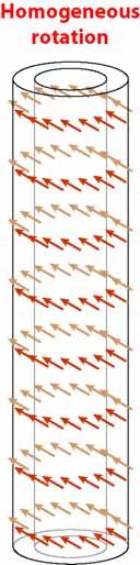
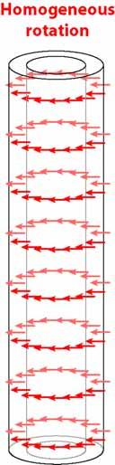
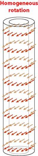
13 Magnetism of Narrow Fe 3 O 4 Tubes 300 K, H // z Oxalic template: D p = 50(±10) nm D int = 105 (±20) nm


14 Magnetism of wider Fe 3 O 4 tubes 300 K, H // z Phosphoric template: D p = 160(±20) nm D int = 460 (±50) nm
15 Questions? D p = 50 nm (d w ) opt = 14 nm D p = 160 nm (d w ) opt = 8 nm Non-monotonic behavior Origin of H c decay Position of optimum
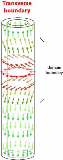
16 Interpretation: Modes of Magnetization Reversal Landeros, Appl. Phys. Lett. 2007, 90,
17 Quantitative Theoretical Modeling Non-monotonic behavior of H c (d w ) reproduced!!! Originates from crossover btw two different reversal modes Absolute values of H c too high
 decreases the")

18 Effect of Stray Fields Interaction of each tube with its neighbors (stray field) decreases the magnetic field it effectively experiences Consequence: lower coercivity J. Escrig et al, PRB 77, (2008).
19 ALD Prozesses for Ferromagnetic Materials 1) Direct Reduction NiCp 2 + H 2 Ni 2) 3-Step Process NiCp 2 + H 2 O + H 2 Ni 3) After ALD-Reduction NiCp 2 + H 2 O NiO NiCp 2 H 2 x times NiCp 2 x times H 2 O NiCp 2 O 3 /H 2 0 x times H 2 Very Low Deposition Rates: <20 pm / cycle Very Granular Metallic Films Low Deposition Rates: 20 to 40 pm / cycle Very Granular Metallic Films H 2 Reduction NiO Ni High Deposition Rates: 0.2 to 0.3 Å / cycle Smooth Metallic Films
 2 and O 3 Pulse M. Daub et al, J. Appl. Phys.")
20 Nickel Nanotubes by ALD Method 1: Reduction during ALD process Three Step ALD Cycle: Ni(Cp) 2, H 2 0 and H 2 Pulse Method 2: Reduction after ALD process ALD Cycle: Ni(Cp) 2 and O 3 Pulse M. Daub et al, J. Appl. Phys. 101, 09J111 (2007).
21 Magnetic Properties of Nickel Nanotubes Tube diameter: 35 nm, wall thickness: nm 2 Co Nanotubes Applied field (Oe)
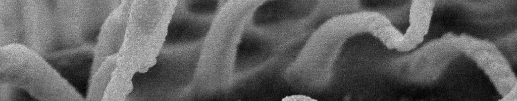
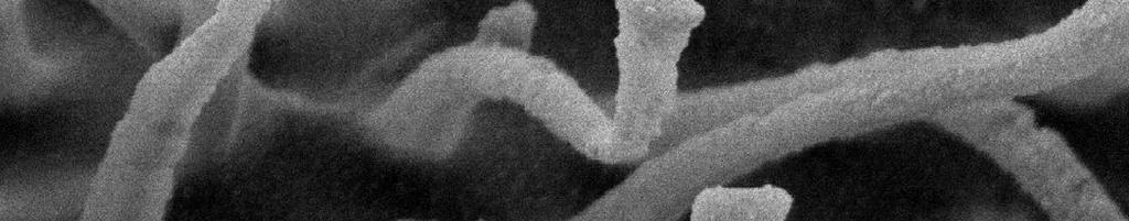
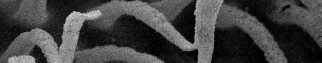
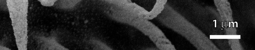
22 Outlook: Multilayer (Magnetic) Nanotubes 200 nm Single-Layer Nanotube Multi-Layer Nanotube 1000 nm 25 nm TiO2 (light), 30 nm Al2O3 (dark) and 35 nm TiO2

 Core-shell Nanotubes and Nanowires J Escrig, D Altbir, and K Nielsch,")
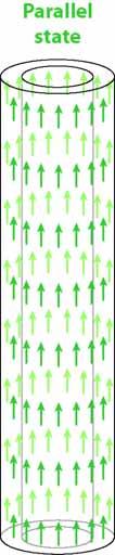
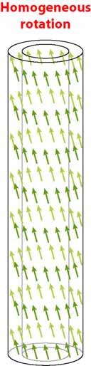
23 Calculations on Bi-Layer Magnetic Nanotubes Detailed Investigations on the magnetic behavior of nanotubes: e.g. potential Transitions: Parallel (β < 0.2) Curling (β = ) Parallel (β >0.8) Core-shell Nanotubes and Nanowires J Escrig, D Altbir, and K Nielsch, Nanotechnology 18, (2007).
24 Outline History and Principle Ferromagnetic Nanostructures Low-Temperature Processes and Biomaterials Novel Synthesis Approach and Nanostructures O u
25 Atomic Layer Deposition (ALD) Chemical vapor deposition (CVD): thermal decomposition on the substrate diffusion rate-limiting Atomic layer deposition (ALD): self-limited reaction with excess reactant layer-by-layer growth

26 ALD on a Complex Substrate

27 ALD on a Complex Substrate
28 Summary of low Temperature Processes M. Knez, K. Nielsch and L. Niinistö, Advanced Materials 19, (2007).

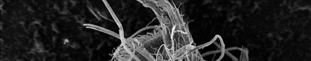
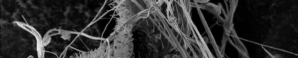
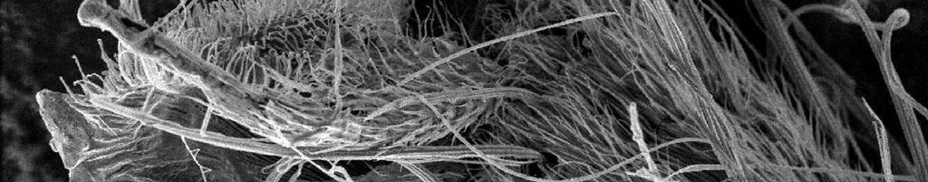
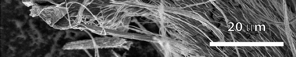
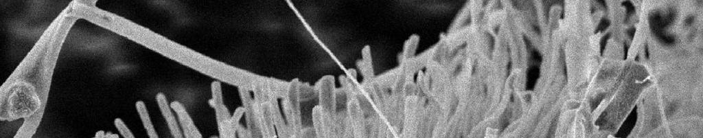
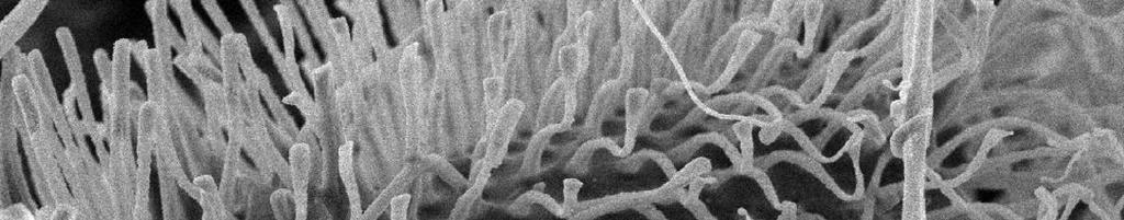
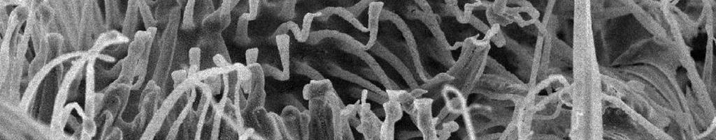
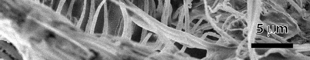
29 Tobacco Mosaic Virus (TMV) Length: 300 nm outer Ø : 18 nm inner Ø : 4 nm RNA T < 80 C 2.8 < ph < 8.5 pi = 3.5 hydrophilic hydrophobic
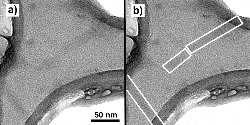
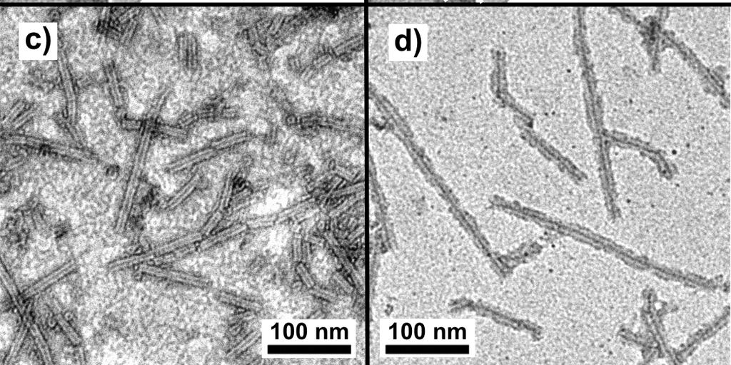
30 TiO 2 -deposition on TMV


31 ALD on Biomaterials M. Knez et al., Nano Lett. 6, 1172 (2006).
32 Outline History and Principle Ferromagnetic Nanostructures Low-Temperature Processes and Biomaterials Novel Synthesis Approach and Nanostructures O u


33 Development of ALD Processes: SiO 2 J. Bachmann et al. Angew. Chemie( 2008).


, 140 nm (NdYAG")
34 Laser Interference Lithography (LIL) Mirror Substrate θ Incoming Light P = λ / 2(sinθ ) Photoresist Substrate θ λ He-Cd Laser λ= 325 nm Rotation Stage Lloyd s Mirror Spatial Filter Limits: 175 nm (HeCd Laser), 140 nm (NdYAG Laser)


35 Nanoring Arrays by IL Lithography and ALD R. Ji et al., in preparation


36 ALD and Solid State Reactions ALD Kirkendall Effect: Material A Festkörperreaktion Solid State Material B Reaction Material A/B H.J. Fan, M. Knez et al., Nature Materials. 5, 627 (2006).


")
37 BMBF Nanotechnology Research Group: Multifunctional Nanowires and Nanotubes Team IAP Uni Hamburg Team MPI-Halle v Christy Chong Jana Sommerlatte Jongmin Lee Ren Bin Yang Financial support by Nachwuchswettbewerb Nanotechnologie : Bundesministerium für Bildung und Forschung (BMBF) German Federal Ministry for Education and Research
High-density data storage: principle
 High-density data storage: principle Current approach High density 1 bit = many domains Information storage driven by domain wall shifts 1 bit = 1 magnetic nanoobject Single-domain needed Single easy axis
Nanostrukturphysik (Nanostructure Physics)
") Nanostrukturphysik (Nanostructure Physics) Prof. Yong Lei & Dr. Yang Xu Fachgebiet 3D-Nanostrukturierung, Institut für Physik Contact: yong.lei@tu-ilmenau.de; yang.xu@tu-ilmenau.de Office: Unterpoerlitzer
Nanostrukturphysik (Nanostructure Physics) Prof. Yong Lei & Dr. Yang Xu Fachgebiet 3D-Nanostrukturierung, Institut für Physik Contact: yong.lei@tu-ilmenau.de; yang.xu@tu-ilmenau.de Office: Unterpoerlitzer
Anisotropy Distributions in Patterned Magnetic Media
 MINT Review & Workshop 24-25 Oct. 2006 Anisotropy Distributions in Patterned Magnetic Media Tom Thomson Hitachi San Jose Research Center Page 1 Acknowledgements Manfred Albrecht (Post-doc) Tom Albrecht
Workshop. GerALD September 22-23, 2008, Max Planck Institute of Microstructure Physics, Halle. FKZ: 03X5507
 Workshop GerALD 2008 September 22-23, 2008, Max Planck Institute of Microstructure Physics, Halle. FKZ: 03X5507 About GerALD: The workshop GerALD is primarily dedicated to the research activities in the
Micro Chemical Vapor Deposition System: Design and Verification
 Micro Chemical Vapor Deposition System: Design and Verification Q. Zhou and L. Lin Berkeley Sensor and Actuator Center, Department of Mechanical Engineering, University of California, Berkeley 2009 IEEE
Magnetic Nanowires inside. carbon nanotubes
 Leibniz Institute for Solid State and Materials Research IFW Dresden Magnetic Nanowires inside Carbon Nanotubes Magnetic force microscopy sensors using ironfilled carbon nanotubes Thomas Mühl Outline Introduction
Recap (so far) Low-Dimensional & Boundary Effects
 Low-Dimensional & Boundary Effects") Recap (so far) Ohm s & Fourier s Laws Mobility & Thermal Conductivity Heat Capacity Wiedemann-Franz Relationship Size Effects and Breakdown of Classical Laws 1 Low-Dimensional & Boundary Effects Energy
Recap (so far) Ohm s & Fourier s Laws Mobility & Thermal Conductivity Heat Capacity Wiedemann-Franz Relationship Size Effects and Breakdown of Classical Laws 1 Low-Dimensional & Boundary Effects Energy
Atomic Layer Deposition of Chalcogenide Thin Films
 Atomic Layer Deposition of Chalcogenide Thin Films PUBLICATION REVIEW ON ULTRATECH ALD SYSTEMS 09.10.2015 1 Highlights Benefits of ALD for nano-manufacturing of chalcogenides Atomic level thickness control
Block Copolymer Based Hybrid Nanostructured Materials As Key Elements In Green Nanotechnology
 The 7 th Korea-U.S. Nano Forum Block Copolymer Based Hybrid Nanostructured Materials As Key Elements In Green Nanotechnology Dong Ha Kim Department of Chemistry and Nano Science, Ewha Womans University
JOHN G. EKERDT RESEARCH FOCUS
 JOHN G. EKERDT RESEARCH FOCUS We study the surface, growth and materials chemistry of metal, dielectric, ferroelectric, and polymer thin films. We seek to understand and describe nucleation and growth
SUPPLEMENTARY INFORMATION
 In the format provided by the authors and unedited. DOI: 10.1038/NNANO.2016.257 Multiple nanostructures based on anodized aluminium oxide templates Liaoyong Wen, Rui Xu, Yan Mi, Yong Lei * 1 NATURE NANOTECHNOLOGY
Step Coverage by ALD Films: Theory and Examples
 Step Coverage by ALD Films: Theory and Examples of Ideal and Non-Ideal Reactions Roy G. Gordon Cambridge, MA 1 L Step Coverage in Holes with High Aspect Ratio Step coverage = (b/a) x 100% a Aspect ratio
Fabrication Methods: Chapter 4. Often two methods are typical. Top Down Bottom up. Begins with atoms or molecules. Begins with bulk materials
 Fabrication Methods: Chapter 4 Often two methods are typical Top Down Bottom up Begins with bulk materials Begins with atoms or molecules Reduced in size to nano By thermal, physical Chemical, electrochemical
There's Plenty of Room at the Bottom
 There's Plenty of Room at the Bottom 12/29/1959 Feynman asked why not put the entire Encyclopedia Britannica (24 volumes) on a pin head (requires atomic scale recording). He proposed to use electron microscope
The goal of this project is to enhance the power density and lowtemperature efficiency of solid oxide fuel cells (SOFC) manufactured by atomic layer
 manufactured by atomic layer") Stanford University Michael Shandalov1, Shriram Ramanathan2, Changhyun Ko2 and Paul McIntyre1 1Department of Materials Science and Engineering, Stanford University 2Division of Engineering and Applied
Stanford University Michael Shandalov1, Shriram Ramanathan2, Changhyun Ko2 and Paul McIntyre1 1Department of Materials Science and Engineering, Stanford University 2Division of Engineering and Applied
Layer-modulated synthesis of uniform tungsten disulfide nanosheet using gas-phase precursors.
 Layer-modulated synthesis of uniform tungsten disulfide nanosheet using gas-phase precursors. Jusang Park * Hyungjun Kim School of Electrical and Electronics Engineering, Yonsei University, 262 Seongsanno,
General Assembly Method for Linear Metal Nanoparticle Chains Embedded in Nanotubes
 General Assembly Method for Linear Metal Nanoparticle Chains Embedded in Nanotubes NANO LETTERS 2008 Vol. 8, No. 10 3221-3225 Yong Qin,* Lifeng Liu, Renbin Yang, Ulrich Gösele, and Mato Knez* Max-Planck-Institute
not to be confused with using the materials to template nanostructures
 Zeolites as Templates: continued Synthesis: Most zeolite syntheses are performed by using template-synthesis not to be confused with using the materials to template nanostructures templates are often surfactants
Understanding Irreducible and Reducible Oxides as Catalysts for Carbon Nanotubes and Graphene Formation
 Wright State University CORE Scholar Special Session 5: Carbon and Oxide Based Nanostructured Materials (2011) Special Session 5 6-2011 Understanding Irreducible and Reducible Oxides as Catalysts for Carbon
JOHN G. EKERDT RESEARCH FOCUS
 JOHN G. EKERDT RESEARCH FOCUS We study the surface, growth and materials chemistry of ultrathin metal and dielectric films. Our work seeks to: 1) develop and understand the reactions and chemistry that
Déposition séléctive le rêve reviens
 Willkommen Welcome Bienvenue Déposition séléctive le rêve reviens Patrik Hoffmann Michael Reinke, Yury Kuzminykh Ivo Utke, Carlos Guerra-Nunez, Ali Dabirian, Xavier Multone, Tristan Bret, Estelle Halary-Wagner,
Surface Functionalization by Atomic Layer Deposition
 Surface Functionalization by Atomic Layer Deposition Christophe Detavernier SIM User Forum - Gent 27/10/2015 CoCooN Conformal Coating of Nanomaterials Atomic layer deposition (ALD) Gas-phase thin film
Thermodynamic calculations on the catalytic growth of carbon nanotubes
 Thermodynamic calculations on the catalytic growth of carbon nanotubes Christian Klinke, Jean-Marc Bonard and Klaus Kern Ecole Polytechnique Federale de Lausanne, CH-05 Lausanne, Switzerland Max-Planck-Institut
Supporting Information for
 Supporting Information for Multilayer CuO@NiO Hollow Spheres: Microwave-Assisted Metal-Organic-Framework Derivation and Highly Reversible Structure-Matched Stepwise Lithium Storage Wenxiang Guo, Weiwei
Platinum ALD from Pt(acac)2 and O3: Growth mechanism and electrocatalytic applications
2 and O3: Growth mechanism and electrocatalytic applications") Platinum ALD from Pt(acac)2 and O3: Growth mechanism and electrocatalytic applications Johannes Schumacher, Loïc Assaud, Alexander Tafel, Julien Bachmann Department of Chemistry and Pharmacy, Friedrich-Alexander-Universität
Platinum ALD from Pt(acac)2 and O3: Growth mechanism and electrocatalytic applications Johannes Schumacher, Loïc Assaud, Alexander Tafel, Julien Bachmann Department of Chemistry and Pharmacy, Friedrich-Alexander-Universität
A Novel Self-aligned and Maskless Process for Formation of Highly Uniform Arrays of Nanoholes and Nanopillars
 Nanoscale Res Lett (2008) 3: 127 DOI 10.1007/s11671-008-9124-6 NANO EXPRESS A Novel Self-aligned and Maskless Process for Formation of Highly Uniform Arrays of Nanoholes and Nanopillars Wei Wu Æ Dibyendu
Nanomaterials and their Optical Applications
 Nanomaterials and their Optical Applications Winter Semester 2013 Lecture 02 rachel.grange@uni-jena.de http://www.iap.uni-jena.de/multiphoton Lecture 2: outline 2 Introduction to Nanophotonics Theoretical
Neutron Reflectometry of Ferromagnetic Arrays
 Neutron Reflectometry of Ferromagnetic Arrays Z.Y. Zhao a, P. Mani a, V.V.Krishnamurthy a, W.-T. Lee b, F. Klose b, and G.J. Mankey a a Center for Materials for Information Technology and Department of
Imaging Polymer Morphology Using Atomic Force Microscopy
 Imaging Polymer Morphology Using Atomic Force Microscopy Russell J. Composto Materials Science and Engineering, and the Laboratory for Research on the Structure of Matter, University of Pennsylvania Agilent
ARC-ASSISTED CO-CONVERSION OF COAL-BASED CARBON AND ACETYLENE
 ARC-ASSISTED CO-CONVERSION OF COAL-BASED CARBON AND ACETYLENE Jieshan Qiu*, Yongfeng Li, Yunpeng Wang Carbon Research Laboratory, Center for Nano Materials and Science, School of Chemical Engineering,
Introduction to Nanotechnology Chapter 5 Carbon Nanostructures Lecture 1
 Introduction to Nanotechnology Chapter 5 Carbon Nanostructures Lecture 1 ChiiDong Chen Institute of Physics, Academia Sinica chiidong@phys.sinica.edu.tw 02 27896766 Carbon contains 6 electrons: (1s) 2,
Multiscale Simulation of Atomic Layer Deposition in a Nanoporous Material
 The Institute for Systems Research Isr Technical Report 28-21 Multiscale Simulation of Atomic Layer Deposition in a Nanoporous Material Dwivedi, Vivek, and Adomaitis, Raymond ISR develops, applies and
Millimeter-Thick Single-Walled Carbon Nanotube Forests: Hidden Role of Catalyst Support
 Millimeter-Thick Single-Walled Carbon Nanotube Forests: Hidden Role of Catalyst Support Suguru Noda 1*, Kei Hasegawa 1, Hisashi Sugime 1, Kazunori Kakehi 1, Zhengyi Zhang 2, Shigeo Maruyama 2 and Yukio
Kim, Sang Ouk
 Directed Block Copolymer Assembly Integrated with Conventional ArF or I-line lithography Kim, ang Ouk (sangouk.kim@kaist.ac.kr) oft Nanomaterials Laboratory (http://snml.kaist.ac.kr) Department of Materials
Large-Area and Uniform Surface-Enhanced Raman. Saturation
 Supporting Information Large-Area and Uniform Surface-Enhanced Raman Spectroscopy Substrate Optimized by Enhancement Saturation Daejong Yang 1, Hyunjun Cho 2, Sukmo Koo 1, Sagar R. Vaidyanathan 2, Kelly
Supplementary Figure 1. (a-b) EDX of Mo 2 and Mo 2
 EDX of Mo 2 and Mo 2") Supplementary Figure 1. (a-b) EDX of Mo 2 C@NPC/NPRGO and Mo 2 C@NPC. Supplementary Figure 2. (a) SEM image of PMo 12 2-PPy, (b) TEM, (c) HRTEM, (d) STEM image and EDX elemental mapping of C, N, P, and
Supplementary Figure 1. (a-b) EDX of Mo 2 C@NPC/NPRGO and Mo 2 C@NPC. Supplementary Figure 2. (a) SEM image of PMo 12 2-PPy, (b) TEM, (c) HRTEM, (d) STEM image and EDX elemental mapping of C, N, P, and
29: Nanotechnology. What is Nanotechnology? Properties Control and Understanding. Nanomaterials
 29: Nanotechnology What is Nanotechnology? Properties Control and Understanding Nanomaterials Making nanomaterials Seeing at the nanoscale Quantum Dots Carbon Nanotubes Biology at the Nanoscale Some Applications
E SC 412 Nanotechnology: Materials, Infrastructure, and Safety Wook Jun Nam
 E SC 412 Nanotechnology: Materials, Infrastructure, and Safety Wook Jun Nam Lecture 17 Outline Colloids and Colloidal Chemistry What is Colloids? Properties of Colloids Examples of Colloids Synthesis of
ALD-enabled nanopatterning: area-selective ALD by area-activation
 ALD-enabled nanopatterning: area-selective ALD by area-activation Adrie Mackus, Ageeth Bol, and Erwin Kessels w.m.m.kessels@tue.nl www.tue.nl/pmp Outline Introduction & Area-selective deposition Area-selective
PROGRESS REPORT FOR AINGRA09119
 Date electronic copy received at AINSE: 14 September 2009 PROGRESS REPORT FOR AINGRA09119 PROJECT TITLE TEM characterisation of novel supported silver and gold nanoparticle catalysts INVESTIGATOR(S) Institution
CARBON NANOSTRUCTURES SYNTHESIZED THROUGH GRAPHITE ETCHING
 CARBON NANOSTRUCTURES SYNTHESIZED THROUGH GRAPHITE ETCHING Q. Yang 1, C. Xiao 1, R. Sammynaiken 2 and A. Hirose 1 1 Plasma Physics Laboratory, University of Saskatchewan, 116 Science Place Saskatoon, SK
Supporting Information
 Electronic Supplementary Material (ESI) for Nanoscale. This journal is The Royal Society of Chemistry 2015 Supporting Information Synthesis and electrochemical properties of spherical and hollow-structured
TiO2/sapphire Beam Splitter for High-order Harmonics
 Technical Communication TiO2/sapphire Beam Splitter for High-order Harmonics Y. Sanjo*1, M. Murata*1, Y. Tanaka*1, H. Kumagai*1, and M. Chigane*2 *1 Graduate School of Engineering,Osaka City University,
Author(s) Tanaka, Yoshitomo; Sumita, Shigekaz. Issue Date (2010) Trans Tech Publications.
 Tanaka, Yoshitomo; Sumita, Shigekaz. Issue Date (2010) Trans Tech Publications.") NAOSITE: Nagasaki University's Ac Title Author(s) Citation Electrodeposition of Ferromagnetic Ohgai, Takeshi; Takao, Keizo; Mizum Tanaka, Yoshitomo; Sumita, Shigekaz Materials Science Forum, 638-642, p
NAOSITE: Nagasaki University's Ac Title Author(s) Citation Electrodeposition of Ferromagnetic Ohgai, Takeshi; Takao, Keizo; Mizum Tanaka, Yoshitomo; Sumita, Shigekaz Materials Science Forum, 638-642, p
Carbon Nanotubes: Development of Nanomaterials for Hydrogen Storage
 Carbon Nanotubes: Development of Nanomaterials for Hydrogen Storage Hongjie Dai Department of Chemistry & Laboratory for Advanced Materials Stanford University GCEP, September 19, 2006 Outline Can carbon
Supporting information:
 Epitaxially Integrating Ferromagnetic Fe 1.3 Ge Nanowire Arrays on Few-Layer Graphene Hana Yoon, Taejoon Kang, Jung Min Lee, Si-in Kim, Kwanyong Seo, Jaemyung Kim, Won Il Park, and Bongsoo Kim,* Department
Tuning the Shell Number of Multi-Shelled Metal Oxide. Hollow Fibers for Optimized Lithium Ion Storage
 Supporting Information Tuning the Shell Number of Multi-Shelled Metal Oxide Hollow Fibers for Optimized Lithium Ion Storage Jin Sun, Chunxiao Lv, Fan Lv, ǁ Shuai Chen, Daohao Li, Ziqi Guo, Wei Han, Dongjiang
ALD Nucleation and Area-Selective Deposition
 ALD Nucleation and Area-Selective Deposition Prof Gregory N. Parsons Department of Chemical and Biomolecular Engineering North Carolina State University Raleigh North Carolina USA 1 Outline 1. Nucleation
2D XRD Imaging by Projection-Type X-Ray Microscope
 0/25 National Institute for Materials Science,Tsukuba, Japan 2D XRD Imaging by Projection-Type X-Ray Microscope 1. Introduction - What s projection-type X-ray microscope? 2. Examples for inhomogeneous/patterned
Supplementary Figure S1. AFM characterizations and topographical defects of h- BN films on silica substrates. (a) (c) show the AFM height
 (c) show the AFM height") Supplementary Figure S1. AFM characterizations and topographical defects of h- BN films on silica substrates. (a) (c) show the AFM height topographies of h-bn film in a size of ~1.5µm 1.5µm, 30µm 30µm
Supplementary Figure S1. AFM characterizations and topographical defects of h- BN films on silica substrates. (a) (c) show the AFM height topographies of h-bn film in a size of ~1.5µm 1.5µm, 30µm 30µm
Rayleigh-Instability-Induced Metal Nanoparticle Chains Encapsulated in Nanotubes Produced by Atomic Layer Deposition
 Rayleigh-Instability-Induced Metal Nanoparticle Chains Encapsulated in Nanotubes Produced by Atomic Layer Deposition NANO LETTERS 2008 Vol. 8, No. 1 114-118 Yong Qin, Seung-Mo Lee, Anlian Pan, Ulrich Go1sele,
29 May 2015 Carbon Nanotube Based Detectors for THz Radiometry
 29 May 2015 Carbon Nanotube Based Detectors for THz Radiometry J.H. Lehman Na#onal Ins#tute of Standards and Technology 325 Broadway, Boulder, Colorado 80305-3228 lehman@boulder.nist.gov Where and Who
Nanostrukturphysik (Nanostructure Physics)
") Nanostrukturphysik (Nanostructure Physics) Prof. Yong Lei & Dr. Yang Xu Fachgebiet 3D-Nanostrukturierung, Institut für Physik Contact: yong.lei@tu-ilmenau.de; yang.xu@tu-ilmenau.de Office: Unterpoerlitzer
Nanostrukturphysik (Nanostructure Physics) Prof. Yong Lei & Dr. Yang Xu Fachgebiet 3D-Nanostrukturierung, Institut für Physik Contact: yong.lei@tu-ilmenau.de; yang.xu@tu-ilmenau.de Office: Unterpoerlitzer
Carbon Nanotube Thin-Films & Nanoparticle Assembly
 Nanodevices using Nanomaterials : Carbon Nanotube Thin-Films & Nanoparticle Assembly Seung-Beck Lee Division of Electronics and Computer Engineering & Department of Nanotechnology, Hanyang University,
Supplemental information. 1. Working principles of CVD and ALD techniques
 Electronic Supplementary Material (ESI) for Energy & Environmental Science. This journal is The Royal Society of Chemistry 2015 Supplemental information 1. Working principles of CVD and ALD techniques
OSCILLATORY THICKNESS DEPENDENCE OF THE COERCIVE FIELD IN MAGNETIC 3D ANTI-DOT ARRAYS
 1 OSCILLATORY THICKNESS DEPENDENCE OF THE COERCIVE FIELD IN MAGNETIC 3D ANTI-DOT ARRAYS A. A. Zhukov 1, M. A. Ghanem 2, A. V. Goncharov 1, R. Boardman 3, V. Novosad 4, G. Karapetrov 4, H. Fangohr 3, P.
Assembled Hollow Metal Oxide Nanostructures for Water Treatment
 UK-China Forum on Nanostructure for Water 11-13 November 2010, The University of Hong Kong Assembled Hollow Metal Oxide Nanostructures for Water Treatment Junbai Li Institute of Chemistry, Beijing CAS
performance electrocatalytic or electrochemical devices. Nanocrystals grown on graphene could have
 Nanocrystal Growth on Graphene with Various Degrees of Oxidation Hailiang Wang, Joshua Tucker Robinson, Georgi Diankov, and Hongjie Dai * Department of Chemistry and Laboratory for Advanced Materials,
PHYSICAL SELF-ASSEMBLY AND NANO-PATTERNING*
 Mater. Res. Soc. Symp. Proc. Vol. 849 2005 Materials Research Society KK8.4.1 PHYSICAL SELF-ASSEMBLY AND NANO-PATTERNING* T.-M. Lu, D.-X. Ye, T. Karabacak, and G.-C. Wang, Department of Physics, Applied
Supporting Information
 Supporting Information Zeolite-Templated Mesoporous Silicon Particles for Advanced Lithium-Ion Battery Anodes Nahyeon Kim, Hyejung Park, Naeun Yoon, and Jung Kyoo Lee * Department of Chemical Engineering,
Calculation of growth per cycle (GPC) of atomic layer deposited aluminium oxide nanolayers and dependence of GPC on surface OH concentration
 of atomic layer deposited aluminium oxide nanolayers and dependence of GPC on surface OH concentration") PRAMANA c Indian Academy of Sciences Vol. 82, No. 3 journal of March 2014 physics pp. 563 569 Calculation of growth per cycle (GPC) of atomic layer deposited aluminium oxide nanolayers and dependence of
PRAMANA c Indian Academy of Sciences Vol. 82, No. 3 journal of March 2014 physics pp. 563 569 Calculation of growth per cycle (GPC) of atomic layer deposited aluminium oxide nanolayers and dependence of
Scanning Probe Microscopy. L. J. Heyderman
 1 Scanning Probe Microscopy 2 Scanning Probe Microscopy If an atom was as large as a ping-pong ball......the tip would have the size of the Matterhorn! 3 Magnetic Force Microscopy Stray field interaction
MURI: Nano-Engineered Energetic. Materials
 MURI: Nano-Engineered Energetic Ralph G. Nuzzo Gregory S. Girolami Anatoly I. Frenkel Ray Twesten Materials The Frederick Seitz Materials Research Laboratory And School of Chemical Sciences University
SUPPLEMENTARY INFORMATION
 SUPPLEMENTARY INFORMATION Facile Synthesis of High Quality Graphene Nanoribbons Liying Jiao, Xinran Wang, Georgi Diankov, Hailiang Wang & Hongjie Dai* Supplementary Information 1. Photograph of graphene
Germanium nanowires: from synthesis, surface chemistry, assembly to devices
 1 Germanium nanowires: from synthesis, surface chemistry, assembly to devices Dunwei Wang Department of Chemistry, Stanford University In order to continue the ever impressive and successful scaling pace
Atomic Layer Deposition of Nanostructured Materials
 Edited by Nicola Pinna and Mato Knez Atomic Layer Deposition of Nanostructured Materials WILEY- VCH WILEY-VCH Verlag GmbH gc. Co. KGaA Contents Foreword V Preface XV/I Introduction XXI List of Contributors
ALIGNED CARBON NANOTUBES FOR MULTIFUNCTIONAL NANOCOMPOSITES AND NANODEVICES:
 ALIGNED CARBON NANOTUBES FOR MULTIFUNCTIONAL NANOCOMPOSITES AND NANODEVICES: Multicomponent Micropatterned Aligned Carbon Nanotube Devices with Reversibly Switchable Electronic Properties for Multifunctional
Formation of Nanostructured Layers for Passivation of High Power Silicon Devices
 Vol. 113 (2008) ACTA PHYSICA POLONICA A No. 3 Proceedings of the 13th International Symposium UFPS, Vilnius, Lithuania 2007 Formation of Nanostructured Layers for Passivation of High Power Silicon Devices
SYNTHESIS OF CARBON NANOTUBES BY CATALYTIC CVD USING Fe-Mo/MgO AND Fe- Mo/Al 2 O 3 CATALYSTS. Abstract. Introduction. Experimental
 SYNTHESIS OF CARBON NANOTUBES BY CATALYTIC CVD USING Fe-Mo/MgO AND Fe- Mo/Al 2 O 3 CATALYSTS Shinn-Shyong Tzeng, Ting-Bin Liang, Sheng-Chuan Wang, Ting-Yu Wu and Yu-Hun Lin Department of Materials Engineering,
Carbon Nanotubes for Interconnect Applications Franz Kreupl, Andrew P. Graham, Maik Liebau, Georg S. Duesberg, Robert Seidel, Eugen Unger
 Carbon Nanotubes for Interconnect Applications Franz Kreupl, Andrew P. Graham, Maik Liebau, Georg S. Duesberg, Robert Seidel, Eugen Unger Infineon Technologies Corporate Research Munich, Germany Outline
Dielectric Meta-Reflectarray for Broadband Linear Polarization Conversion and Optical Vortex Generation
 Supporting Information Dielectric Meta-Reflectarray for Broadband Linear Polarization Conversion and Optical Vortex Generation Yuanmu Yang, Wenyi Wang, Parikshit Moitra, Ivan I. Kravchenko, Dayrl P. Briggs,
Electronic Supplementary Information
 Electronic Supplementary Material (ESI) for Journal of Materials Chemistry C. This journal is The Royal Society of Chemistry 2017 Electronic Supplementary Information Trifunctional NiO Ag NiO Electrodes
Novel Tooling for Scaling of High Quality CVD Graphene Production. Karlheinz Strobl, Mathieu Monville, Riju Singhal and Samuel Wright
 Novel Tooling for Scaling of High Quality CVD Graphene Production Karlheinz Strobl, Mathieu Monville, Riju Singhal and Samuel Wright 1 Commercialization of Nano Materials Commercialization Volume production
Nanostrukturphysik Übung 2 (Class 3&4)
") Nanostrukturphysik Übung 2 (Class 3&4) Prof. Yong Lei & Dr. Yang Xu 2017.05.03 Fachgebiet 3D-Nanostrukturierung, Institut für Physik Contact: yong.lei@tu-ilmenau.de (3748), yang.xu@tuilmenau.de (4902)
Nanostrukturphysik Übung 2 (Class 3&4) Prof. Yong Lei & Dr. Yang Xu 2017.05.03 Fachgebiet 3D-Nanostrukturierung, Institut für Physik Contact: yong.lei@tu-ilmenau.de (3748), yang.xu@tuilmenau.de (4902)
Making the Invisible Visible: Probing Antiferromagnetic Order in Novel Materials
 Making the Invisible Visible: Probing Antiferromagnetic Order in Novel Materials Elke Arenholz Lawrence Berkeley National Laboratory Antiferromagnetic contrast in X-ray absorption Ni in NiO Neel Temperature
Ni-Co bimetal nanowires filled multiwalled carbon nanotubes for the highly. sensitive and selective non-enzymatic glucose sensor applications
 Ni-Co bimetal nanowires filled multiwalled carbon nanotubes for the highly sensitive and selective non-enzymatic glucose sensor applications K. Ramachandran, T. Raj kumar, K. Justice Babu & G. Gnana kumar
Honeycomb-like Interconnected Network of Nickel Phosphide Hetero-nanoparticles
 Supporting Information Honeycomb-like Interconnected Network of Nickel Phosphide Hetero-nanoparticles with Superior Electrochemical Performance for Supercapacitors Shude Liu a, Kalimuthu Vijaya Sankar
Growth window and possible mechanism of millimeter-thick single-walled carbon nanotube forests
 Growth window and possible mechanism of millimeter-thick single-walled carbon nanotube forests Kei Hasegawa 1, Suguru Noda 1,*, Hisashi Sugime 1, Kazunori Kakehi 1, Shigeo Maruyama 2 and Yukio Yamaguchi
Anti-icing surfaces based on enhanced self-propelled jumping of condensed water microdroplets
 Anti-icing surfaces based on enhanced self-propelled jumping of condensed water microdroplets Qiaolan Zhang, a,b Min He, a Jing Chen, a,b Jianjun Wang,* a Yanlin Song* a and Lei Jiang a a Beijing National
Manufacture of Nanostructures for Power Electronics Applications
 Manufacture of Nanostructures for Power Electronics Applications Brian Hunt and Jon Lai Etamota Corporation 2672 E. Walnut St. Pasadena, CA 91107 APEC, Palm Springs Feb. 23rd, 2010 1 Background Outline
Revelation of the Excellent Intrinsic Activity. Evolution Reaction in Alkaline Medium
 Supporting Information Revelation of the Excellent Intrinsic Activity of MoS2 NiS MoO3 Nanowires for Hydrogen Evolution Reaction in Alkaline Medium Chuanqin Wang a,b, Bin Tian b, Mei Wu b, Jiahai Wang
Investigation on the growth of CNTs from SiO x and Fe 2 O 3 nanoparticles by in situ TEM
 The 5 th Workshop on Nucleation and Growth Mechanisms of SWCNTs Investigation on the growth of CNTs from SiO x and Fe 2 O 3 nanoparticles by in situ TEM Chang Liu Shenyang National Laboratory for Materials
NANOMEDICINE. WILEY A John Wiley and Sons, Ltd., Publication DESIGN AND APPLICATIONS OF MAGNETIC NANOMATERIALS, NANOSENSORS AND NANOSYSTEMS
 NANOMEDICINE DESIGN AND APPLICATIONS OF MAGNETIC NANOMATERIALS, NANOSENSORS AND NANOSYSTEMS Vijay K. Varadan Linfeng Chen Jining Xie WILEY A John Wiley and Sons, Ltd., Publication Preface About the Authors
Short course on Atomic Layer Deposition
 Short course on Atomic Layer Deposition Erwin Kessels & Jan-Pieter van Delft w.m.m.kessels@tue.nl www.phys.tue.nl/pmp Vapor phase deposition technologies Physical Vapor Deposition (PVD) sputtering Chemical
Electric-field-directed growth of carbon nanotubes in two dimensions
 Electric-field-directed growth of carbon nanotubes in two dimensions Alireza Nojeh a),b) Department of Electrical Engineering, Stanford University, Stanford, California 94305 Ant Ural b),c) Department
Fabrication and Measurement of Spin Devices. Purdue Birck Presentation
 Fabrication and Measurement of Spin Devices Zhihong Chen School of Electrical and Computer Engineering Birck Nanotechnology Center, Discovery Park Purdue University Purdue Birck Presentation zhchen@purdue.edu
Supplementary Figure S1 Anticrossing and mode exchange between D1 (Wood's anomaly)
") Supplementary Figure S1 Anticrossing and mode exchange between D1 (Wood's anomaly) and D3 (Fabry Pérot cavity mode). (a) Schematic (top) showing the reflectance measurement geometry and simulated angle-resolved
Supplementary Figure S1 Anticrossing and mode exchange between D1 (Wood's anomaly) and D3 (Fabry Pérot cavity mode). (a) Schematic (top) showing the reflectance measurement geometry and simulated angle-resolved
Thermal Transport in Graphene and other Two-Dimensional Systems. Li Shi. Department of Mechanical Engineering & Texas Materials Institute
 Thermal Transport in Graphene and other Two-Dimensional Systems Li Shi Department of Mechanical Engineering & Texas Materials Institute Outline Thermal Transport Theories and Simulations of Graphene Raman
Fabrication and Domain Imaging of Iron Magnetic Nanowire Arrays
 Abstract #: 983 Program # MI+NS+TuA9 Fabrication and Domain Imaging of Iron Magnetic Nanowire Arrays D. A. Tulchinsky, M. H. Kelley, J. J. McClelland, R. Gupta, R. J. Celotta National Institute of Standards
Harvesting Heat through Seebeck Spin Tunneling Effect
 Harvesting Heat through Seebeck Spin Tunneling Effect Costel Constantin James Madison University Science Enabled by Photon Source, May 2012 Outline 1. Spintronics vs. Spin Caloritronics. 2. Novel Spin
Revealing High Fidelity of Nanomolding Process by Extracting the Information from AFM Image with Systematic Artifacts
 Revealing High Fidelity of Nanomolding Process by Extracting the Information from AFM Image with Systematic Artifacts Sajal Biring* Department of Electronics Engineering and Organic Electronics Research
Lattice-Oriented Growth of Single-Walled Carbon Nanotubes
 Letter Subscriber access provided by DUKE UNIV Lattice-Oriented Growth of Single-Walled Carbon Nanotubes Ming Su, Yan Li, Benjamin Maynor, Alper Buldum, Jian Ping Lu, and Jie Liu J. Phys. Chem. B, 2000,
TRANSVERSE SPIN TRANSPORT IN GRAPHENE
 International Journal of Modern Physics B Vol. 23, Nos. 12 & 13 (2009) 2641 2646 World Scientific Publishing Company TRANSVERSE SPIN TRANSPORT IN GRAPHENE TARIQ M. G. MOHIUDDIN, A. A. ZHUKOV, D. C. ELIAS,
Supplementary Information. Atomic Layer Deposition of Platinum Catalysts on Nanowire Surfaces for Photoelectrochemical Water Reduction
 Supplementary Information Atomic Layer Deposition of Platinum Catalysts on Nanowire Surfaces for Photoelectrochemical Water Reduction Neil P. Dasgupta 1 ǂ, Chong Liu 1,2 ǂ, Sean Andrews 1,2, Fritz B. Prinz
Efficient Hydrogen Evolution. University of Central Florida, 4000 Central Florida Blvd. Orlando, Florida, 32816,
 Electronic Supplementary Material (ESI) for Energy & Environmental Science. This journal is The Royal Society of Chemistry 2017 MoS 2 /TiO 2 Heterostructures as Nonmetal Plasmonic Photocatalysts for Highly
Introduction to Nanotechnology Chapter 5 Carbon Nanostructures Lecture 1
 Introduction to Nanotechnology Chapter 5 Carbon Nanostructures Lecture 1 ChiiDong Chen Institute of Physics, Academia Sinica chiidong@phys.sinica.edu.tw 02 27896766 Section 5.2.1 Nature of the Carbon Bond
Thierry Djenizian. Fabrication de microbatteries Li-ion à base de nanotubes de TiO2. Department of Flexible Electronics, CMP Gardanne
 Department of Flexible Electronics, CMP Gardanne Fabrication de microbatteries Li-ion à base de nanotubes de TiO2 Thierry Djenizian 2 All-solid-state microbatteries Motivation : shrink the size of power
Selective Processes: Challenges and Opportunities in Semiconductor Scaling
 Selective Processes: Challenges and Opportunities in Semiconductor Scaling June 4, 2018 Kandabara Tapily TEL Technology Center, America, LLC IITC 2018 Selective Deposition Workshop K. Tapily/ IITC 2018
ALD high-k and higher-k integration on GaAs
 ALD high-k and higher-k integration on GaAs Ozhan Koybasi 1), Min Xu 1), Yiqun Liu 2), Jun-Jieh Wang 2), Roy G. Gordon 2), and Peide D. Ye 1)* 1) School of Electrical and Computer Engineering, Purdue University,
NANOCATALYSIS ON NOVEL SUPPORTS GRAPHENE SHEETS AND HIGHLY POROUS COORDINATION POLYMERS
 NANOCATALYSIS ON NOVEL SUPPORTS GRAPHENE SHEETS AND HIGHLY POROUS COORDINATION POLYMERS M. Samy El-Shall Department of Chemistry Virginia Commonwealth University Richmond, Virginia 23284-2006 IWAM-09,